EP3707976B1 - Elektronische vorrichtung mit magnetisch befestigtem elektronikbauteil - Google Patents
Elektronische vorrichtung mit magnetisch befestigtem elektronikbauteil Download PDFInfo
- Publication number
- EP3707976B1 EP3707976B1 EP18830020.6A EP18830020A EP3707976B1 EP 3707976 B1 EP3707976 B1 EP 3707976B1 EP 18830020 A EP18830020 A EP 18830020A EP 3707976 B1 EP3707976 B1 EP 3707976B1
- Authority
- EP
- European Patent Office
- Prior art keywords
- housing
- electronic component
- internal surface
- electronic device
- magnetic
- Prior art date
- Legal status (The legal status is an assumption and is not a legal conclusion. Google has not performed a legal analysis and makes no representation as to the accuracy of the status listed.)
- Active
Links
Images



Classifications
-
- H—ELECTRICITY
- H05—ELECTRIC TECHNIQUES NOT OTHERWISE PROVIDED FOR
- H05K—PRINTED CIRCUITS; CASINGS OR CONSTRUCTIONAL DETAILS OF ELECTRIC APPARATUS; MANUFACTURE OF ASSEMBLAGES OF ELECTRICAL COMPONENTS
- H05K5/00—Casings, cabinets or drawers for electric apparatus
- H05K5/02—Details
- H05K5/0217—Mechanical details of casings
-
- G—PHYSICS
- G06—COMPUTING OR CALCULATING; COUNTING
- G06F—ELECTRIC DIGITAL DATA PROCESSING
- G06F1/00—Details not covered by groups G06F3/00 - G06F13/00 and G06F21/00
- G06F1/16—Constructional details or arrangements
- G06F1/1613—Constructional details or arrangements for portable computers
- G06F1/1633—Constructional details or arrangements of portable computers not specific to the type of enclosures covered by groups G06F1/1615 - G06F1/1626
- G06F1/1656—Details related to functional adaptations of the enclosure, e.g. to provide protection against EMI, shock, water, or to host detachable peripherals like a mouse or removable expansions units like PCMCIA cards, or to provide access to internal components for maintenance or to removable storage supports like CDs or DVDs, or to mechanically mount accessories
- G06F1/1658—Details related to functional adaptations of the enclosure, e.g. to provide protection against EMI, shock, water, or to host detachable peripherals like a mouse or removable expansions units like PCMCIA cards, or to provide access to internal components for maintenance or to removable storage supports like CDs or DVDs, or to mechanically mount accessories related to the mounting of internal components, e.g. disc drive or any other functional module
-
- G—PHYSICS
- G06—COMPUTING OR CALCULATING; COUNTING
- G06F—ELECTRIC DIGITAL DATA PROCESSING
- G06F1/00—Details not covered by groups G06F3/00 - G06F13/00 and G06F21/00
- G06F1/16—Constructional details or arrangements
- G06F1/18—Packaging or power distribution
- G06F1/183—Internal mounting support structures, e.g. for supporting printed circuit boards
-
- G—PHYSICS
- G06—COMPUTING OR CALCULATING; COUNTING
- G06F—ELECTRIC DIGITAL DATA PROCESSING
- G06F1/00—Details not covered by groups G06F3/00 - G06F13/00 and G06F21/00
- G06F1/16—Constructional details or arrangements
- G06F1/18—Packaging or power distribution
- G06F1/183—Internal mounting support structures, e.g. for supporting printed circuit boards
- G06F1/184—Mounting of motherboards
-
- H—ELECTRICITY
- H05—ELECTRIC TECHNIQUES NOT OTHERWISE PROVIDED FOR
- H05K—PRINTED CIRCUITS; CASINGS OR CONSTRUCTIONAL DETAILS OF ELECTRIC APPARATUS; MANUFACTURE OF ASSEMBLAGES OF ELECTRICAL COMPONENTS
- H05K13/00—Apparatus or processes specially adapted for manufacturing or adjusting assemblages of electric components
- H05K13/0015—Orientation; Alignment; Positioning
-
- H—ELECTRICITY
- H05—ELECTRIC TECHNIQUES NOT OTHERWISE PROVIDED FOR
- H05K—PRINTED CIRCUITS; CASINGS OR CONSTRUCTIONAL DETAILS OF ELECTRIC APPARATUS; MANUFACTURE OF ASSEMBLAGES OF ELECTRICAL COMPONENTS
- H05K13/00—Apparatus or processes specially adapted for manufacturing or adjusting assemblages of electric components
- H05K13/08—Monitoring manufacture of assemblages
-
- H—ELECTRICITY
- H05—ELECTRIC TECHNIQUES NOT OTHERWISE PROVIDED FOR
- H05K—PRINTED CIRCUITS; CASINGS OR CONSTRUCTIONAL DETAILS OF ELECTRIC APPARATUS; MANUFACTURE OF ASSEMBLAGES OF ELECTRICAL COMPONENTS
- H05K3/00—Apparatus or processes for manufacturing printed circuits
- H05K3/30—Assembling printed circuits with electric components, e.g. with resistors
- H05K3/303—Assembling printed circuits with electric components, e.g. with resistors with surface mounted components
- H05K3/305—Affixing by adhesive
-
- H—ELECTRICITY
- H05—ELECTRIC TECHNIQUES NOT OTHERWISE PROVIDED FOR
- H05K—PRINTED CIRCUITS; CASINGS OR CONSTRUCTIONAL DETAILS OF ELECTRIC APPARATUS; MANUFACTURE OF ASSEMBLAGES OF ELECTRICAL COMPONENTS
- H05K5/00—Casings, cabinets or drawers for electric apparatus
- H05K5/0017—Casings, cabinets or drawers for electric apparatus with operator interface units
-
- H—ELECTRICITY
- H05—ELECTRIC TECHNIQUES NOT OTHERWISE PROVIDED FOR
- H05K—PRINTED CIRCUITS; CASINGS OR CONSTRUCTIONAL DETAILS OF ELECTRIC APPARATUS; MANUFACTURE OF ASSEMBLAGES OF ELECTRICAL COMPONENTS
- H05K7/00—Constructional details common to different types of electric apparatus
- H05K7/14—Mounting supporting structure in casing or on frame or rack
- H05K7/1417—Mounting supporting structure in casing or on frame or rack having securing means for mounting boards, plates or wiring boards
-
- H—ELECTRICITY
- H05—ELECTRIC TECHNIQUES NOT OTHERWISE PROVIDED FOR
- H05K—PRINTED CIRCUITS; CASINGS OR CONSTRUCTIONAL DETAILS OF ELECTRIC APPARATUS; MANUFACTURE OF ASSEMBLAGES OF ELECTRICAL COMPONENTS
- H05K2201/00—Indexing scheme relating to printed circuits covered by H05K1/00
- H05K2201/10—Details of components or other objects attached to or integrated in a printed circuit board
- H05K2201/10431—Details of mounted components
- H05K2201/10507—Involving several components
- H05K2201/10537—Attached components
-
- H—ELECTRICITY
- H05—ELECTRIC TECHNIQUES NOT OTHERWISE PROVIDED FOR
- H05K—PRINTED CIRCUITS; CASINGS OR CONSTRUCTIONAL DETAILS OF ELECTRIC APPARATUS; MANUFACTURE OF ASSEMBLAGES OF ELECTRICAL COMPONENTS
- H05K2203/00—Indexing scheme relating to apparatus or processes for manufacturing printed circuits covered by H05K3/00
- H05K2203/10—Using electric, magnetic and electromagnetic fields; Using laser light
- H05K2203/104—Using magnetic force, e.g. to align particles or for a temporary connection during processing
Definitions
- Screws provide a robust and secure connection between the circuit board and the housing or chassis of the electronic device.
- using screws during manufacturing of an electronic device requires a long duration of cycle time.
- a typical motherboard for a laptop computing device with a CPU may require 10 to 15 screws to mount the motherboard to the laptop, which creates a long duration of cycle time on the assembly line as each screw must be manually installed.
- Using screws to attach the motherboard also presents re-workability challenges during manufacturing. In order to rework any component on the motherboard, all of the screws must be removed and the motherboard must be detached completely from the housing or chassis of the device.
- a typical re-work rate for a motherboard of a laptop may be as high as 5 to 10%.
- JP2002217559A relates to a magnet mounted on an AS-i slave, which works as an interface with various actuators and a sensor controlled by a master in an open network, and thereby the slave can be mounted on a device by means of the magnet.
- WO2017111842 discloses a mobile device comprising a printed circuit board having ferromagnetic elements coupled to magnets arranged on the rear surface of the display to fix the the circuit board within the housing.
- the ferromagnetic elements are configured to be pulled by an external magnet of a dock station having a heat sink in order to pull the circuit board towards the rear housing cover to bring heat source components on the circuit board in thermal contact with the rear housing cover and the heat sink of the dock station.
- FIG. 1 is an illustration of an environment 100 in an example implementation that is operable to employ the electronic device with a magnetically attached electronic component described herein.
- Environment 100 includes examples of an electronic device 102, may be configured in a variety of ways.
- an electronic device 102 may be configured as a tablet computing device, a laptop computing device, a desktop computer, a smartphone, or a gaming system.
- the electronic device 102 may also be implemented as a peripheral device, such as a speaker, a keyboard, and so forth.
- the electronic device 102 is not limited by these examples, and may correspond to any type of electronic device or product.
- the electronic device 102 may range from full resource devices with substantial memory and processor resources (e.g., personal computers, game consoles) to a low-resource device with limited memory and/or processing resources (e.g., mobile devices).
- full resource devices with substantial memory and processor resources (e.g., personal computers, game consoles)
- a low-resource device with limited memory and/or processing resources e.g., mobile devices.
- An example device is described in more detail with regards to FIG. 6 .
- Electronic device 102 is further illustrated as including a housing 106 and one or more electronic components 108.
- the housing 106 of electronic device 102 corresponds to an enclosure, case, or chassis which encloses the one or more electronic components 108 of the electronic device 102.
- the housing 106 of electronic device 102 may be formed from a variety of different materials, and take on a variety of different form factors based on the type of device.
- the form factor for the housing 106 of a tablet computing device is different than the form factor of the housing of a desktop computer, a smartphone, a head-mounted augmented reality (AR) or virtual (VR) device, and so forth.
- AR augmented reality
- VR virtual
- the electronic component 108 corresponds to a motherboard of the electronic device 102.
- a motherboard is the main printed circuit board (PCB) found within electronic devices 102, and often includes many of the critical components essential to the functioning of the electronic device, such as the CPU, GPU, RAM, and so forth.
- the electronic components 108 of electronic device 102 may correspond to any type of electronic component that is found within a housing of the device, such as PCBs and circuit boards other than the motherboard, displays, speakers, and so forth.
- the housing 106 includes both external surfaces which are visible, as well as internal surfaces 110 which are not visible when the electronic device 102 is assembled. Unlike conventional electronic devices with "screwed-in" electronic components, the electronic component 108 of the electronic device 102 is magnetically attached to an internal surface of the housing 106 via a magnetic force between the electronic component and the internal surface of the housing.
- the magnet protrudes from the internal surface 110 of the housing 106 and extends into a cavity on the corresponding magnetic element on the electronic component 108 to magnetically attach the electronic component 108 to the internal surface 110 of the housing 106.
- Example 200 further illustrates an electronic component 108, which as discussed above, may correspond to any type of electronic component, such as a motherboard.
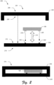
- a magnetic force 214 enables the electronic component 108 to magnetically attach to internal surface 212 of bottom housing portion 204 when the electronic component 108 is positioned within a certain proximity of the internal surface 212 to form the magnetic attachment.
- the magnetic force 214 enables the magnetic attachment without the use of screws.
- FIG. 3 illustrates an additional example 300 of an electronic component which can be magnetically attached to an internal surface of a housing of an electronic device via multiple magnets on the internal surface of the housing and corresponding magnetic elements on the electronic component.
- the magnets 304 are secured to the internal surface 302 of the housing after the housing is manufactured via an adhesive, such as by gluing the magnets 304 to the internal surface 302 of the housing 106. Doing so enables manufacture of a clean chassis, which reduces the complexity, and thus costs, associated with manufacturing the chassis.
- Conventional devices manufacture the chassis to include "bosses" which are configured to receive screws to secure the electronic component to the chassis.
- the magnets may be formed as part of the housing.
- an electronic component 108 is illustrated with a form factor corresponding to a motherboard for the electronic device 102.
- the electronic component 108 includes magnetic elements 306-1, 306-2, 306-3, 306-4, 306-5, 306-6, 306-7, 306-8, and 306-9, which are configured to align with corresponding magnets 304-1, 304-2, 304-3, 304-4, 304-5, 304-6, 304-7, 304-8, and 304-9 of the internal surface 302 of electronic device 102.
- Each magnetic element 306 of the electronic component 108 includes a cavity which is configured to receive the protrusion of the respective magnet of the internal surface of the housing in order to form the magnetic attachment.
- the electronic component 108 can be magnetically attached to the internal surface of the housing 106 of electronic device 102 as a manual or automated process. For example, in some cases an automated machine or assembly process may be utilized to attach the electronic component 108 to the electronic device.
- Device manufacturing system 402 is further illustrated as including a testing module 412, which is configured to test various components of the assembled electronic device 102 to detect errors.
- the testing module 412 may test various components of the electronic component when implemented as a motherboard, such as CPU, GPU, and so forth, to ensure that the attached electronic component is functioning properly.
- the testing module 412 may detect errors in the electronic component, which requires the electronic component to be removed and "re-worked".
- FIG. 5 depicts an example procedure 500 of magnetically attaching an electronic component to an internal surface of a housing of an electronic device. Aspects of this procedure may be implemented in hardware, firmware, or software, or a combination thereof.
- the procedures are shown as a set of blocks that specify operations performed by one or more devices and are not necessarily limited to the orders shown for performing the operations by the respective blocks.
- the example computing device 602 as illustrated includes a processing system 604, one or more computer-readable media 606, and one or more I/O interface 608 that are communicatively coupled, one to another.
- the computing device 602 may further include a system bus or other data and command transfer system that couples the various components, one to another.
- a system bus can include any one or combination of different bus structures, such as a memory bus or memory controller, a peripheral bus, a universal serial bus, and/or a processor or local bus that utilizes any of a variety of bus architectures.
- a variety of other examples are also contemplated, such as control and data lines.
- the computer-readable storage media 606 is illustrated as including memory/storage 612.
- the memory/storage 612 represents memory/storage capacity associated with one or more computer-readable media.
- the memory/storage component 612 may include volatile media (such as random access memory (RAM)) and/or nonvolatile media (such as read only memory (ROM), Flash memory, optical disks, magnetic disks, and so forth).
- the memory/storage component 612 may include fixed media (e.g., RAM, ROM, a fixed hard drive, and so on) as well as removable media (e.g., Flash memory, a removable hard drive, an optical disc, and so forth).
- the computer-readable media 606 may be configured in a variety of other ways as further described below.
- Input/output interface(s) 608 are representative of functionality to allow a user to enter commands and information to computing device 602, and also allow information to be presented to the user and/or other components or devices using various input/output devices.
- input devices include a keyboard, a cursor control device (e.g., a mouse), a microphone, a scanner, touch functionality (e.g., capacitive or other sensors that are configured to detect physical touch), a camera (e.g., which may employ visible or non-visible wavelengths such as infrared frequencies to recognize movement as gestures that do not involve touch), and so forth.
- Examples of output devices include a display device (e.g., a monitor or projector), speakers, a printer, a network card, tactile-response device, and so forth.
- the computing device 602 may be configured in a variety of ways as further described below to support user interaction.
- modules include routines, programs, objects, elements, components, data structures, and so forth that perform particular tasks or implement particular abstract data types.
- module generally represent software, firmware, hardware, or a combination thereof.
- the features of the techniques described herein are platform-independent, meaning that the techniques may be implemented on a variety of commercial computing platforms having a variety of processors.
- Examples of computer-readable storage media may include, but are not limited to, RAM, ROM, EEPROM, flash memory or other memory technology, CD-ROM, digital versatile disks (DVD) or other optical storage, hard disks, magnetic cassettes, magnetic tape, magnetic disk storage or other magnetic storage devices, or other storage device, tangible media, or article of manufacture suitable to store the desired information and which may be accessed by a computer.
- Computer-readable signal media may refer to a signal-bearing medium that is configured to transmit instructions to the hardware of the computing device 602, such as via a network.
- Signal media typically may embody computer readable instructions, data structures, program modules, or other data in a modulated data signal, such as carrier waves, data signals, or other transport mechanism.
- Signal media also include any information delivery media.
- modulated data signal means a signal that has one or more of its characteristics set or changed in such a manner as to encode information in the signal.
- communication media include wired media such as a wired network or direct-wired connection, and wireless media such as acoustic, RF, infrared, and other wireless media.
- hardware elements 610 and computer-readable media 606 are representative of modules, programmable device logic and/or fixed device logic implemented in a hardware form that may be employed in some examples to implement at least some aspects of the techniques described herein, such as to perform one or more instructions.
- Hardware may include components of an integrated circuit or on-chip system, an application-specific integrated circuit (ASIC), a field-programmable gate array (FPGA), a complex programmable logic device (CPLD), and other implementations in silicon or other hardware.
- ASIC application-specific integrated circuit
- FPGA field-programmable gate array
- CPLD complex programmable logic device
- hardware may operate as a processing device that performs program tasks defined by instructions and/or logic embodied by the hardware as well as a hardware utilized to store instructions for execution, e.g., the computer-readable storage media described previously.
- software, hardware, or executable modules may be implemented as one or more instructions and/or logic embodied on some form of computer-readable storage media and/or by one or more hardware elements 610.
- the computing device 602 may be configured to implement particular instructions and/or functions corresponding to the software and/or hardware modules. Accordingly, implementation of a module that is executable by the computing device 602 as software may be achieved at least partially in hardware, e.g., through use of computer-readable storage media and/or hardware elements 610 of the processing system 604.
- the instructions and/or functions may be executable/operable by one or more articles of manufacture (for example, one or more computing devices 602 and/or processing systems 604) to implement techniques, modules, and examples described herein.
- the example system 600 enables ubiquitous environments for a seamless user experience when running applications on a personal computer (PC), a television device, and/or a mobile device. Services and applications run substantially similar in all three environments for a common user experience when transitioning from one device to the next while utilizing an application, playing a video game, watching a video, and so on.
- PC personal computer
- television device a television device
- mobile device a mobile device. Services and applications run substantially similar in all three environments for a common user experience when transitioning from one device to the next while utilizing an application, playing a video game, watching a video, and so on.
- multiple devices are interconnected through a central computing device.
- the central computing device may be local to the multiple devices or may be located remotely from the multiple devices.
- the central computing device may be a cloud of one or more server computers that are connected to the multiple devices through a network, the Internet, or other data communication link.
- this interconnection architecture enables functionality to be delivered across multiple devices to provide a common and seamless experience to a user of the multiple devices.
- Each of the multiple devices may have different physical requirements and capabilities, and the central computing device uses a platform to enable the delivery of an experience to the device that is both tailored to the device and yet common to all devices.
- a class of target devices is created and experiences are tailored to the generic class of devices.
- a class of devices may be defined by physical features, types of usage, or other common characteristics of the devices.
- the computing device 602 may assume a variety of different configurations, such as for computer 614, mobile 616, and television 618 uses. Each of these configurations includes devices that may have generally different constructs and capabilities, and thus the computing device 602 may be configured according to one or more of the different device classes. For instance, the computing device 602 may be implemented as the computer 614 class of a device that includes a personal computer, desktop computer, a multi-screen computer, laptop computer, netbook, and so on.
- the computing device 602 may also be implemented as the mobile 616 class of device that includes mobile devices, such as a mobile phone, wearables (e.g., wrist bands, pendants, rings, etc.) portable music player, portable gaming device, a tablet computer, a multi-screen computer, and so on.
- the computing device 602 may also be implemented as the television 618 class of device that includes devices having or connected to generally larger screens in casual viewing environments. These devices include televisions, set-top boxes, gaming consoles, and so on. Other devices are also contemplated, such as appliances, thermostats and so on as part of the "Internet of Things.”
- the techniques described herein may be supported by these various configurations of the computing device 602 and are not limited to the specific examples of the techniques described herein. This functionality may also be implemented all or in part through use of a distributed system, such as over a "cloud" 620 via a platform 622 as described below.
- the cloud 620 includes and/or is representative of a platform 622 for resources 624.
- the platform 622 abstracts underlying functionality of hardware (e.g., servers) and software resources of the cloud 620.
- the resources 624 may include applications and/or data that can be utilized while computer processing is executed on servers that are remote from the computing device 602.
- Resources 624 can also include services provided over the Internet and/or through a subscriber network, such as a cellular or Wi-Fi network.
- the platform 622 may abstract resources and functions to connect the computing device 602 with other computing devices.
- the platform 622 may also serve to abstract scaling of resources to provide a corresponding level of scale to encountered demand for the resources 624 that are implemented via the platform 622. Accordingly, in an interconnected device, implementation of functionality described herein may be distributed throughout the system 600. For example, the functionality may be implemented in part on the computing device 602 as well as via the platform 622 that abstracts the functionality of the cloud 620.
Landscapes
- Engineering & Computer Science (AREA)
- Theoretical Computer Science (AREA)
- Computer Hardware Design (AREA)
- Microelectronics & Electronic Packaging (AREA)
- General Engineering & Computer Science (AREA)
- Human Computer Interaction (AREA)
- Physics & Mathematics (AREA)
- General Physics & Mathematics (AREA)
- Manufacturing & Machinery (AREA)
- Power Engineering (AREA)
- Operations Research (AREA)
- Casings For Electric Apparatus (AREA)
Claims (12)
- Elektronische Vorrichtung (102, 200), umfassend:ein Gehäuse (106, 206), das einen oberen Abschnitt (202) und einen unteren Abschnitt (204) gegenüber dem oberen Abschnitt aufweist; undein elektronisches Bauteil (108) für die elektronische Vorrichtung (102), wobei das elektronische Bauteil (108) innerhalb des Gehäuses (106, 206) angeordnet und mittels einer Magnetkraft zwischen einem oder mehreren magnetischen Befestigungspunkten (218, 220) des elektronischen Bauteils (108) und einem oder mehreren entsprechenden magnetischen Befestigungspunkten (222, 224) an der Innenoberfläche des unteren Abschnitts des Gehäuses (106) magnetisch an einer Innenoberfläche (110) des unteren Abschnitts des Gehäuses (106) befestigt ist,wobei der eine oder die mehreren entsprechenden magnetischen Befestigungspunkte an der Innenoberfläche des unteren Abschnitts des Gehäuses eine Vielzahl von Magneten umfassen und der eine oder die mehreren magnetischen Befestigungspunkte an dem elektronischen Bauteil eine Vielzahl von magnetischen Elementen an dem elektronischen Bauteil umfassen, die jeweils magnetisch an der Vielzahl von Magneten befestigt sind,wobei die Vielzahl von Magneten von der Innenoberfläche des Gehäuses hervorstehen und sich in eine Vielzahl von Hohlräumen der jeweiligen Vielzahl von magnetischen Elementen an dem elektronischen Bauteil erstrecken, um das elektronische Bauteil magnetisch an der Innenoberfläche des unteren Abschnitts des Gehäuses zu befestigen, undwobei jedes der magnetischen Elemente eine an dem elektronischen Bauteil befestigte Mutter umfasst und wobei jeder der Hohlräume einem Loch der Mutter entspricht.
- Elektronische Vorrichtung nach Anspruch 1, wobei das elektronische Bauteil eine Leiterplatte ist und wobei die Leiterplatte eine Hauptleiterplatte umfasst.
- Elektronische Vorrichtung nach Anspruch 1, wobei die Vielzahl von Magneten mittels eines Klebstoffs mit der Innenoberfläche des unteren Abschnitts des Gehäuses verbunden sind.
- Elektronische Vorrichtung nach Anspruch 1, wobei die Vielzahl von Magneten als Teil des Gehäuses ausgebildet sind.
- Elektronische Vorrichtung nach Anspruch 1, wobei ferner ein oder mehrere magnetische Befestigungspunkte des elektronischen Bauteils einen Magneten an dem elektronischen Bauteil einschließen, der magnetisch an einem entsprechenden magnetischen Element an der Innenoberfläche des unteren Abschnitts des Gehäuses befestigt ist.
- Elektronische Vorrichtung nach Anspruch 5, wobei die Innenoberfläche des Gehäuses aus einem magnetischen Material gebildet ist und wobei eine magnetische Befestigung dadurch gebildet wird, dass ein oder mehrere Magneten des elektronischen Bauteils magnetisch an dem magnetischen Material der Innenoberfläche des Gehäuses haften.
- Elektronische Vorrichtung nach Anspruch 1, ferner umfassend ein Ausrichtungsmerkmal zum Ausrichten des elektronischen Bauelements mit der Innenoberfläche des unteren Abschnitts des Gehäuses, wobei das Ausrichtungsmerkmal einen Vorsprung an der Innenoberfläche des unteren Abschnitts des Gehäuses umfasst, der sich in ein entsprechendes Loch oder einen entsprechenden Hohlraum an dem elektronischen Bauteil oder durch dieses/diesen hindurch erstreckt.
- Elektronische Vorrichtung nach Anspruch 1, die als Tablet-Vorrichtung konfiguriert ist.
- Elektronische Vorrichtung nach Anspruch 1, wobei der obere Abschnitt eine Anzeige umfasst und wobei das elektronische Bauteil zwischen der Innenoberfläche des unteren Abschnitts des Gehäuses und der Anzeige positioniert ist.
- Elektronische Vorrichtung nach Anspruch 9, wobei der obere Abschnitt, der die Anzeige umfasst, magnetisch an dem Gehäuse befestigt ist.
- Computerimplementiertes Verfahren (500), das durch ein Vorrichtungsherstellungssystem implementiert wird, um ein elektronisches Bauteil magnetisch an einer Innenoberfläche eines unteren Abschnitts eines Gehäuses einer elektronischen Vorrichtung (200) nach einem der Ansprüche 1 bis 10 zu befestigen, wobei das Verfahren umfasst:Erhalten (502), durch das Vorrichtungsherstellungssystem, des Gehäuses (206) und des elektronischen Bauteils (108) der elektronischen Vorrichtung; Vorrichtung (200); undSteuern (504) von Maschinen des Vorrichtungsherstellungssystems, um den einen oder die mehreren magnetischen Befestigungspunkte (218, 220) des elektronischen Bauteils innerhalb magnetischer Nähe auf den einen oder die mehreren entsprechenden magnetischen Befestigungspunkte (222, 224) einer Innenoberfläche des unteren Abschnitts (204) des Gehäuses der elektronischen Vorrichtung auszurichten, um das elektronische Bauteil magnetisch an der Innenoberfläche des unteren Abschnitts (204) des Gehäuses zu befestigen.
- Computerimplementiertes Verfahren nach Anspruch 11, ferner umfassend:Testen des magnetisch befestigten elektronischen Bauteils, um einen oder mehrere Fehler in dem elektronischen Bauteil zu erkennen;als Reaktion auf das Erkennen eines oder mehrerer Fehler Entfernen des magnetisch befestigten elektronischen Bauteils von der Innenoberfläche des unteren Abschnitts des Gehäuses; undals Reaktion auf das Beheben des einen oder der mehreren Fehler, Steuern der Maschinen des Vorrichtungsherstellungssystems, um den einen oder die mehreren magnetischen Befestigungspunkte des elektronischen Bauteils innerhalb magnetischer Nähe auf den einen oder die mehreren entsprechenden magnetischen Befestigungspunkte einer Innenoberfläche des unteren Abschnitts des Gehäuses der elektronischen Vorrichtung auszurichten, um das elektronische Bauteil magnetisch an der Innenoberfläche des unteren Abschnitts des Gehäuses zu befestigen.
Applications Claiming Priority (2)
| Application Number | Priority Date | Filing Date | Title |
|---|---|---|---|
| US15/807,343 US10555427B2 (en) | 2017-11-08 | 2017-11-08 | Electronic device with a magnetically attached electronic component |
| PCT/US2018/058601 WO2019094246A1 (en) | 2017-11-08 | 2018-11-01 | Electronic device with a magnetically attached electronic component |
Publications (2)
| Publication Number | Publication Date |
|---|---|
| EP3707976A1 EP3707976A1 (de) | 2020-09-16 |
| EP3707976B1 true EP3707976B1 (de) | 2024-07-10 |
Family
ID=64949372
Family Applications (1)
| Application Number | Title | Priority Date | Filing Date |
|---|---|---|---|
| EP18830020.6A Active EP3707976B1 (de) | 2017-11-08 | 2018-11-01 | Elektronische vorrichtung mit magnetisch befestigtem elektronikbauteil |
Country Status (3)
| Country | Link |
|---|---|
| US (1) | US10555427B2 (de) |
| EP (1) | EP3707976B1 (de) |
| WO (1) | WO2019094246A1 (de) |
Families Citing this family (2)
| Publication number | Priority date | Publication date | Assignee | Title |
|---|---|---|---|---|
| JP2025521147A (ja) * | 2022-05-29 | 2025-07-08 | レモニ エー/エス | 容易に取付け可能な無線データ通信ユニット及びそれを備えるシステム |
| US12530055B2 (en) * | 2023-06-15 | 2026-01-20 | Microsoft Technology Licensing, Llc | Secure electromagnetic docking system |
Citations (4)
| Publication number | Priority date | Publication date | Assignee | Title |
|---|---|---|---|---|
| WO2012024578A2 (en) * | 2010-08-19 | 2012-02-23 | Apple Inc. | Portable electronic device |
| US20130135552A1 (en) * | 2011-11-29 | 2013-05-30 | Shenzhen China Star Optoelectronics Technology Co., Ltd. | Printed Circuit Board and Liquid Crystal Display Module |
| US20140192470A1 (en) * | 2013-01-09 | 2014-07-10 | Giga-Byte Technology Co., Ltd. | Upper lid body of laptop |
| WO2017111842A1 (en) * | 2015-12-26 | 2017-06-29 | Intel Corporation | Adjustable gap structure for mobile devices |
Family Cites Families (21)
| Publication number | Priority date | Publication date | Assignee | Title |
|---|---|---|---|---|
| JPS6339442U (de) * | 1986-08-29 | 1988-03-14 | ||
| JPS63275198A (ja) | 1987-05-07 | 1988-11-11 | Fujitsu Ltd | プリント板の取着構造 |
| JP2002217559A (ja) | 2001-01-23 | 2002-08-02 | Fuji Electric Co Ltd | AS−iスレーブ |
| JP2002368449A (ja) | 2001-06-04 | 2002-12-20 | Matsushita Electric Ind Co Ltd | 磁気記録再生装置 |
| TW552182B (en) * | 2002-10-08 | 2003-09-11 | Jian-Shing Lin | Magnetic socket |
| JP2007073125A (ja) | 2005-09-06 | 2007-03-22 | Hitachi Global Storage Technologies Netherlands Bv | 磁気記録再生装置 |
| WO2007062268A2 (en) * | 2005-11-28 | 2007-05-31 | University Of Florida Research Foundation, Inc. | Method and structure for magnetically-directed, self-assembly of three-dimensional structures |
| KR101641229B1 (ko) | 2009-10-23 | 2016-07-20 | 엘지전자 주식회사 | 확장 모듈 및 이를 구비한 휴대 전자기기 |
| TWI482565B (zh) * | 2011-04-13 | 2015-04-21 | Wistron Corp | 印刷電路板、支撐治具以及定位方法 |
| US8475285B2 (en) | 2011-08-04 | 2013-07-02 | Megatouch, Llc | Swinging motherboard for amusement device |
| KR101829395B1 (ko) | 2011-09-01 | 2018-02-20 | 삼성전자주식회사 | 표시장치 |
| US10495946B2 (en) * | 2012-02-03 | 2019-12-03 | Case-Mate, Inc. | Illumination device |
| US8947874B2 (en) * | 2012-06-08 | 2015-02-03 | Bartley K. Andre | Portable computing device with a housing secured by a magnetic element and related method |
| KR20140002102A (ko) * | 2012-06-26 | 2014-01-08 | 삼성디스플레이 주식회사 | 표시 장치 |
| KR20140100325A (ko) * | 2013-02-06 | 2014-08-14 | 삼성전자주식회사 | 발광 소자 패키지 모듈 |
| US9474345B2 (en) | 2013-08-13 | 2016-10-25 | Apple Inc. | Magnetic related features of a cover for an electronic device |
| JP2015082637A (ja) * | 2013-10-24 | 2015-04-27 | 富士通株式会社 | 部品集合体の製造方法、位置決め装置 |
| US9665125B2 (en) | 2014-03-28 | 2017-05-30 | Intel Corporation | Magnetic attachment mechanism for an electronic device |
| US9600034B2 (en) * | 2015-02-13 | 2017-03-21 | Google Inc. | Attaching computing device to mount by magnets |
| KR102483377B1 (ko) * | 2015-11-30 | 2023-01-02 | 삼성전자주식회사 | 전자 장치 및 전자 장치 제조방법 |
| KR102094873B1 (ko) * | 2016-05-10 | 2020-03-31 | 삼성디스플레이 주식회사 | 표시 장치, 휴대용 단말기, 및 표시 장치의 작동 방법 |
-
2017
- 2017-11-08 US US15/807,343 patent/US10555427B2/en active Active
-
2018
- 2018-11-01 WO PCT/US2018/058601 patent/WO2019094246A1/en not_active Ceased
- 2018-11-01 EP EP18830020.6A patent/EP3707976B1/de active Active
Patent Citations (4)
| Publication number | Priority date | Publication date | Assignee | Title |
|---|---|---|---|---|
| WO2012024578A2 (en) * | 2010-08-19 | 2012-02-23 | Apple Inc. | Portable electronic device |
| US20130135552A1 (en) * | 2011-11-29 | 2013-05-30 | Shenzhen China Star Optoelectronics Technology Co., Ltd. | Printed Circuit Board and Liquid Crystal Display Module |
| US20140192470A1 (en) * | 2013-01-09 | 2014-07-10 | Giga-Byte Technology Co., Ltd. | Upper lid body of laptop |
| WO2017111842A1 (en) * | 2015-12-26 | 2017-06-29 | Intel Corporation | Adjustable gap structure for mobile devices |
Also Published As
| Publication number | Publication date |
|---|---|
| US10555427B2 (en) | 2020-02-04 |
| US20190141846A1 (en) | 2019-05-09 |
| EP3707976A1 (de) | 2020-09-16 |
| WO2019094246A1 (en) | 2019-05-16 |
Similar Documents
| Publication | Publication Date | Title |
|---|---|---|
| US9073123B2 (en) | Housing vents | |
| JP6921277B2 (ja) | 目標検出追跡方法、装置、電子デバイス、記憶媒体、及びプログラム | |
| US20150227231A1 (en) | Virtual Transparent Display | |
| EP3707976B1 (de) | Elektronische vorrichtung mit magnetisch befestigtem elektronikbauteil | |
| EP3129850B1 (de) | Dünne wärmeübertragungsvorrichtung für wärmeverwaltung | |
| CN107111470A (zh) | 浏览器显示投射技术 | |
| JP6625123B2 (ja) | ディスプレイモジュールサポート | |
| US10684962B2 (en) | Vendor-specific peripheral device class identifiers | |
| EP3248098A1 (de) | Steuerung der zugabe von repräsentationen an einen anwendungsstarter | |
| US9762849B2 (en) | Super-resolution processing method for TV video images, super-resolution processing device for TV video images that is used in same method, first to fourteenth super-resolution processing programs, and first to fourth storage media | |
| KR20170055983A (ko) | 컴퓨터에서의 개별 디바이스 리셋 및 복구 | |
| CN206272738U (zh) | 电视主板及电视机 | |
| US9306344B2 (en) | Computing device connectors | |
| US20160147931A1 (en) | Programmable cad system suited for preventing interference between component and chassis, and method thereof | |
| KR20130029706A (ko) | 이미지 테스트에 관한 이미지 데이터를 처리하기 위한 시스템 및 방법 | |
| TWI584242B (zh) | 電子看板 | |
| CN103514313A (zh) | 一种信息处理方法 | |
| US20210201843A1 (en) | Bases interfacing with electronic devices | |
| US20170004802A1 (en) | Digital signage | |
| CN104977982A (zh) | 通用型电子设备组合 | |
| TW201539311A (zh) | 通用型電子設備組合 |
Legal Events
| Date | Code | Title | Description |
|---|---|---|---|
| STAA | Information on the status of an ep patent application or granted ep patent |
Free format text: STATUS: UNKNOWN |
|
| STAA | Information on the status of an ep patent application or granted ep patent |
Free format text: STATUS: THE INTERNATIONAL PUBLICATION HAS BEEN MADE |
|
| PUAI | Public reference made under article 153(3) epc to a published international application that has entered the european phase |
Free format text: ORIGINAL CODE: 0009012 |
|
| STAA | Information on the status of an ep patent application or granted ep patent |
Free format text: STATUS: REQUEST FOR EXAMINATION WAS MADE |
|
| 17P | Request for examination filed |
Effective date: 20200424 |
|
| AK | Designated contracting states |
Kind code of ref document: A1 Designated state(s): AL AT BE BG CH CY CZ DE DK EE ES FI FR GB GR HR HU IE IS IT LI LT LU LV MC MK MT NL NO PL PT RO RS SE SI SK SM TR |
|
| AX | Request for extension of the european patent |
Extension state: BA ME |
|
| DAV | Request for validation of the european patent (deleted) | ||
| DAX | Request for extension of the european patent (deleted) | ||
| RAP3 | Party data changed (applicant data changed or rights of an application transferred) |
Owner name: MICROSOFT TECHNOLOGY LICENSING, LLC |
|
| STAA | Information on the status of an ep patent application or granted ep patent |
Free format text: STATUS: EXAMINATION IS IN PROGRESS |
|
| 17Q | First examination report despatched |
Effective date: 20220218 |
|
| GRAP | Despatch of communication of intention to grant a patent |
Free format text: ORIGINAL CODE: EPIDOSNIGR1 |
|
| STAA | Information on the status of an ep patent application or granted ep patent |
Free format text: STATUS: GRANT OF PATENT IS INTENDED |
|
| RIC1 | Information provided on ipc code assigned before grant |
Ipc: G06F 1/16 20060101ALI20231231BHEP Ipc: G06F 1/18 20060101ALI20231231BHEP Ipc: H05K 7/14 20060101AFI20231231BHEP |
|
| INTG | Intention to grant announced |
Effective date: 20240201 |
|
| P01 | Opt-out of the competence of the unified patent court (upc) registered |
Effective date: 20240313 |
|
| GRAS | Grant fee paid |
Free format text: ORIGINAL CODE: EPIDOSNIGR3 |
|
| GRAA | (expected) grant |
Free format text: ORIGINAL CODE: 0009210 |
|
| STAA | Information on the status of an ep patent application or granted ep patent |
Free format text: STATUS: THE PATENT HAS BEEN GRANTED |
|
| AK | Designated contracting states |
Kind code of ref document: B1 Designated state(s): AL AT BE BG CH CY CZ DE DK EE ES FI FR GB GR HR HU IE IS IT LI LT LU LV MC MK MT NL NO PL PT RO RS SE SI SK SM TR |
|
| REG | Reference to a national code |
Ref country code: CH Ref legal event code: EP |
|
| REG | Reference to a national code |
Ref country code: DE Ref legal event code: R096 Ref document number: 602018071659 Country of ref document: DE |
|
| REG | Reference to a national code |
Ref country code: LT Ref legal event code: MG9D |
|
| REG | Reference to a national code |
Ref country code: NL Ref legal event code: MP Effective date: 20240710 |
|
| PG25 | Lapsed in a contracting state [announced via postgrant information from national office to epo] |
Ref country code: PT Free format text: LAPSE BECAUSE OF FAILURE TO SUBMIT A TRANSLATION OF THE DESCRIPTION OR TO PAY THE FEE WITHIN THE PRESCRIBED TIME-LIMIT Effective date: 20241111 |
|
| REG | Reference to a national code |
Ref country code: AT Ref legal event code: MK05 Ref document number: 1703186 Country of ref document: AT Kind code of ref document: T Effective date: 20240710 |
|
| PG25 | Lapsed in a contracting state [announced via postgrant information from national office to epo] |
Ref country code: NL Free format text: LAPSE BECAUSE OF FAILURE TO SUBMIT A TRANSLATION OF THE DESCRIPTION OR TO PAY THE FEE WITHIN THE PRESCRIBED TIME-LIMIT Effective date: 20240710 |
|
| PG25 | Lapsed in a contracting state [announced via postgrant information from national office to epo] |
Ref country code: PT Free format text: LAPSE BECAUSE OF FAILURE TO SUBMIT A TRANSLATION OF THE DESCRIPTION OR TO PAY THE FEE WITHIN THE PRESCRIBED TIME-LIMIT Effective date: 20241111 Ref country code: NL Free format text: LAPSE BECAUSE OF FAILURE TO SUBMIT A TRANSLATION OF THE DESCRIPTION OR TO PAY THE FEE WITHIN THE PRESCRIBED TIME-LIMIT Effective date: 20240710 |
|
| PG25 | Lapsed in a contracting state [announced via postgrant information from national office to epo] |
Ref country code: NO Free format text: LAPSE BECAUSE OF FAILURE TO SUBMIT A TRANSLATION OF THE DESCRIPTION OR TO PAY THE FEE WITHIN THE PRESCRIBED TIME-LIMIT Effective date: 20241010 |
|
| PG25 | Lapsed in a contracting state [announced via postgrant information from national office to epo] |
Ref country code: FI Free format text: LAPSE BECAUSE OF FAILURE TO SUBMIT A TRANSLATION OF THE DESCRIPTION OR TO PAY THE FEE WITHIN THE PRESCRIBED TIME-LIMIT Effective date: 20240710 Ref country code: GR Free format text: LAPSE BECAUSE OF FAILURE TO SUBMIT A TRANSLATION OF THE DESCRIPTION OR TO PAY THE FEE WITHIN THE PRESCRIBED TIME-LIMIT Effective date: 20241011 Ref country code: PL Free format text: LAPSE BECAUSE OF FAILURE TO SUBMIT A TRANSLATION OF THE DESCRIPTION OR TO PAY THE FEE WITHIN THE PRESCRIBED TIME-LIMIT Effective date: 20240710 |
|
| PG25 | Lapsed in a contracting state [announced via postgrant information from national office to epo] |
Ref country code: BG Free format text: LAPSE BECAUSE OF FAILURE TO SUBMIT A TRANSLATION OF THE DESCRIPTION OR TO PAY THE FEE WITHIN THE PRESCRIBED TIME-LIMIT Effective date: 20240710 |
|
| PG25 | Lapsed in a contracting state [announced via postgrant information from national office to epo] |
Ref country code: LV Free format text: LAPSE BECAUSE OF FAILURE TO SUBMIT A TRANSLATION OF THE DESCRIPTION OR TO PAY THE FEE WITHIN THE PRESCRIBED TIME-LIMIT Effective date: 20240710 |
|
| PG25 | Lapsed in a contracting state [announced via postgrant information from national office to epo] |
Ref country code: IS Free format text: LAPSE BECAUSE OF FAILURE TO SUBMIT A TRANSLATION OF THE DESCRIPTION OR TO PAY THE FEE WITHIN THE PRESCRIBED TIME-LIMIT Effective date: 20241110 Ref country code: AT Free format text: LAPSE BECAUSE OF FAILURE TO SUBMIT A TRANSLATION OF THE DESCRIPTION OR TO PAY THE FEE WITHIN THE PRESCRIBED TIME-LIMIT Effective date: 20240710 |
|
| PG25 | Lapsed in a contracting state [announced via postgrant information from national office to epo] |
Ref country code: HR Free format text: LAPSE BECAUSE OF FAILURE TO SUBMIT A TRANSLATION OF THE DESCRIPTION OR TO PAY THE FEE WITHIN THE PRESCRIBED TIME-LIMIT Effective date: 20240710 |
|
| PG25 | Lapsed in a contracting state [announced via postgrant information from national office to epo] |
Ref country code: RS Free format text: LAPSE BECAUSE OF FAILURE TO SUBMIT A TRANSLATION OF THE DESCRIPTION OR TO PAY THE FEE WITHIN THE PRESCRIBED TIME-LIMIT Effective date: 20241010 Ref country code: ES Free format text: LAPSE BECAUSE OF FAILURE TO SUBMIT A TRANSLATION OF THE DESCRIPTION OR TO PAY THE FEE WITHIN THE PRESCRIBED TIME-LIMIT Effective date: 20240710 |
|
| PG25 | Lapsed in a contracting state [announced via postgrant information from national office to epo] |
Ref country code: RS Free format text: LAPSE BECAUSE OF FAILURE TO SUBMIT A TRANSLATION OF THE DESCRIPTION OR TO PAY THE FEE WITHIN THE PRESCRIBED TIME-LIMIT Effective date: 20241010 Ref country code: PL Free format text: LAPSE BECAUSE OF FAILURE TO SUBMIT A TRANSLATION OF THE DESCRIPTION OR TO PAY THE FEE WITHIN THE PRESCRIBED TIME-LIMIT Effective date: 20240710 Ref country code: NO Free format text: LAPSE BECAUSE OF FAILURE TO SUBMIT A TRANSLATION OF THE DESCRIPTION OR TO PAY THE FEE WITHIN THE PRESCRIBED TIME-LIMIT Effective date: 20241010 Ref country code: LV Free format text: LAPSE BECAUSE OF FAILURE TO SUBMIT A TRANSLATION OF THE DESCRIPTION OR TO PAY THE FEE WITHIN THE PRESCRIBED TIME-LIMIT Effective date: 20240710 Ref country code: IS Free format text: LAPSE BECAUSE OF FAILURE TO SUBMIT A TRANSLATION OF THE DESCRIPTION OR TO PAY THE FEE WITHIN THE PRESCRIBED TIME-LIMIT Effective date: 20241110 Ref country code: HR Free format text: LAPSE BECAUSE OF FAILURE TO SUBMIT A TRANSLATION OF THE DESCRIPTION OR TO PAY THE FEE WITHIN THE PRESCRIBED TIME-LIMIT Effective date: 20240710 Ref country code: GR Free format text: LAPSE BECAUSE OF FAILURE TO SUBMIT A TRANSLATION OF THE DESCRIPTION OR TO PAY THE FEE WITHIN THE PRESCRIBED TIME-LIMIT Effective date: 20241011 Ref country code: FI Free format text: LAPSE BECAUSE OF FAILURE TO SUBMIT A TRANSLATION OF THE DESCRIPTION OR TO PAY THE FEE WITHIN THE PRESCRIBED TIME-LIMIT Effective date: 20240710 Ref country code: ES Free format text: LAPSE BECAUSE OF FAILURE TO SUBMIT A TRANSLATION OF THE DESCRIPTION OR TO PAY THE FEE WITHIN THE PRESCRIBED TIME-LIMIT Effective date: 20240710 Ref country code: BG Free format text: LAPSE BECAUSE OF FAILURE TO SUBMIT A TRANSLATION OF THE DESCRIPTION OR TO PAY THE FEE WITHIN THE PRESCRIBED TIME-LIMIT Effective date: 20240710 Ref country code: AT Free format text: LAPSE BECAUSE OF FAILURE TO SUBMIT A TRANSLATION OF THE DESCRIPTION OR TO PAY THE FEE WITHIN THE PRESCRIBED TIME-LIMIT Effective date: 20240710 |
|
| REG | Reference to a national code |
Ref country code: DE Ref legal event code: R097 Ref document number: 602018071659 Country of ref document: DE |
|
| PG25 | Lapsed in a contracting state [announced via postgrant information from national office to epo] |
Ref country code: RO Free format text: LAPSE BECAUSE OF FAILURE TO SUBMIT A TRANSLATION OF THE DESCRIPTION OR TO PAY THE FEE WITHIN THE PRESCRIBED TIME-LIMIT Effective date: 20240710 Ref country code: SM Free format text: LAPSE BECAUSE OF FAILURE TO SUBMIT A TRANSLATION OF THE DESCRIPTION OR TO PAY THE FEE WITHIN THE PRESCRIBED TIME-LIMIT Effective date: 20240710 Ref country code: DK Free format text: LAPSE BECAUSE OF FAILURE TO SUBMIT A TRANSLATION OF THE DESCRIPTION OR TO PAY THE FEE WITHIN THE PRESCRIBED TIME-LIMIT Effective date: 20240710 |
|
| PG25 | Lapsed in a contracting state [announced via postgrant information from national office to epo] |
Ref country code: EE Free format text: LAPSE BECAUSE OF FAILURE TO SUBMIT A TRANSLATION OF THE DESCRIPTION OR TO PAY THE FEE WITHIN THE PRESCRIBED TIME-LIMIT Effective date: 20240710 |
|
| PG25 | Lapsed in a contracting state [announced via postgrant information from national office to epo] |
Ref country code: CZ Free format text: LAPSE BECAUSE OF FAILURE TO SUBMIT A TRANSLATION OF THE DESCRIPTION OR TO PAY THE FEE WITHIN THE PRESCRIBED TIME-LIMIT Effective date: 20240710 |
|
| PG25 | Lapsed in a contracting state [announced via postgrant information from national office to epo] |
Ref country code: SK Free format text: LAPSE BECAUSE OF FAILURE TO SUBMIT A TRANSLATION OF THE DESCRIPTION OR TO PAY THE FEE WITHIN THE PRESCRIBED TIME-LIMIT Effective date: 20240710 Ref country code: IT Free format text: LAPSE BECAUSE OF FAILURE TO SUBMIT A TRANSLATION OF THE DESCRIPTION OR TO PAY THE FEE WITHIN THE PRESCRIBED TIME-LIMIT Effective date: 20240710 |
|
| PLBE | No opposition filed within time limit |
Free format text: ORIGINAL CODE: 0009261 |
|
| STAA | Information on the status of an ep patent application or granted ep patent |
Free format text: STATUS: NO OPPOSITION FILED WITHIN TIME LIMIT |
|
| 26N | No opposition filed |
Effective date: 20250411 |
|
| REG | Reference to a national code |
Ref country code: CH Ref legal event code: PL |
|
| PG25 | Lapsed in a contracting state [announced via postgrant information from national office to epo] |
Ref country code: MC Free format text: LAPSE BECAUSE OF FAILURE TO SUBMIT A TRANSLATION OF THE DESCRIPTION OR TO PAY THE FEE WITHIN THE PRESCRIBED TIME-LIMIT Effective date: 20240710 |
|
| PG25 | Lapsed in a contracting state [announced via postgrant information from national office to epo] |
Ref country code: LU Free format text: LAPSE BECAUSE OF NON-PAYMENT OF DUE FEES Effective date: 20241101 |
|
| REG | Reference to a national code |
Ref country code: CH Ref legal event code: PL |
|
| PG25 | Lapsed in a contracting state [announced via postgrant information from national office to epo] |
Ref country code: CH Free format text: LAPSE BECAUSE OF NON-PAYMENT OF DUE FEES Effective date: 20241130 |
|
| REG | Reference to a national code |
Ref country code: BE Ref legal event code: MM Effective date: 20241130 |
|
| PG25 | Lapsed in a contracting state [announced via postgrant information from national office to epo] |
Ref country code: SE Free format text: LAPSE BECAUSE OF FAILURE TO SUBMIT A TRANSLATION OF THE DESCRIPTION OR TO PAY THE FEE WITHIN THE PRESCRIBED TIME-LIMIT Effective date: 20240710 |
|
| PG25 | Lapsed in a contracting state [announced via postgrant information from national office to epo] |
Ref country code: BE Free format text: LAPSE BECAUSE OF NON-PAYMENT OF DUE FEES Effective date: 20241130 |
|
| PG25 | Lapsed in a contracting state [announced via postgrant information from national office to epo] |
Ref country code: IE Free format text: LAPSE BECAUSE OF NON-PAYMENT OF DUE FEES Effective date: 20241101 |
|
| PGFP | Annual fee paid to national office [announced via postgrant information from national office to epo] |
Ref country code: DE Payment date: 20251022 Year of fee payment: 8 |
|
| PGFP | Annual fee paid to national office [announced via postgrant information from national office to epo] |
Ref country code: GB Payment date: 20251023 Year of fee payment: 8 |
|
| PGFP | Annual fee paid to national office [announced via postgrant information from national office to epo] |
Ref country code: FR Payment date: 20251023 Year of fee payment: 8 |
|
| PG25 | Lapsed in a contracting state [announced via postgrant information from national office to epo] |
Ref country code: HU Free format text: LAPSE BECAUSE OF FAILURE TO SUBMIT A TRANSLATION OF THE DESCRIPTION OR TO PAY THE FEE WITHIN THE PRESCRIBED TIME-LIMIT; INVALID AB INITIO Effective date: 20181101 |
|
| PG25 | Lapsed in a contracting state [announced via postgrant information from national office to epo] |
Ref country code: CY Free format text: LAPSE BECAUSE OF FAILURE TO SUBMIT A TRANSLATION OF THE DESCRIPTION OR TO PAY THE FEE WITHIN THE PRESCRIBED TIME-LIMIT; INVALID AB INITIO Effective date: 20181101 |