EP3706285B1 - Verfahren und vorrichtung zum drahtlosen laden und system zum drahtlosen laden - Google Patents
Verfahren und vorrichtung zum drahtlosen laden und system zum drahtlosen laden Download PDFInfo
- Publication number
- EP3706285B1 EP3706285B1 EP18881348.9A EP18881348A EP3706285B1 EP 3706285 B1 EP3706285 B1 EP 3706285B1 EP 18881348 A EP18881348 A EP 18881348A EP 3706285 B1 EP3706285 B1 EP 3706285B1
- Authority
- EP
- European Patent Office
- Prior art keywords
- receiver
- transmitter
- voltage
- load
- wireless charging
- Prior art date
- Legal status (The legal status is an assumption and is not a legal conclusion. Google has not performed a legal analysis and makes no representation as to the accuracy of the status listed.)
- Active
Links
Images






Classifications
-
- H—ELECTRICITY
- H02—GENERATION; CONVERSION OR DISTRIBUTION OF ELECTRIC POWER
- H02J—ELECTRIC POWER NETWORKS; CIRCUIT ARRANGEMENTS OR SYSTEMS FOR SUPPLYING OR DISTRIBUTING ELECTRIC POWER; SYSTEMS FOR STORING ELECTRIC ENERGY
- H02J50/00—Circuit arrangements or systems for wireless supply or distribution of electric power
- H02J50/10—Circuit arrangements or systems for wireless supply or distribution of electric power using inductive coupling
-
- H—ELECTRICITY
- H02—GENERATION; CONVERSION OR DISTRIBUTION OF ELECTRIC POWER
- H02J—ELECTRIC POWER NETWORKS; CIRCUIT ARRANGEMENTS OR SYSTEMS FOR SUPPLYING OR DISTRIBUTING ELECTRIC POWER; SYSTEMS FOR STORING ELECTRIC ENERGY
- H02J50/00—Circuit arrangements or systems for wireless supply or distribution of electric power
- H02J50/10—Circuit arrangements or systems for wireless supply or distribution of electric power using inductive coupling
- H02J50/12—Circuit arrangements or systems for wireless supply or distribution of electric power using inductive coupling of the resonant type
-
- H—ELECTRICITY
- H02—GENERATION; CONVERSION OR DISTRIBUTION OF ELECTRIC POWER
- H02J—ELECTRIC POWER NETWORKS; CIRCUIT ARRANGEMENTS OR SYSTEMS FOR SUPPLYING OR DISTRIBUTING ELECTRIC POWER; SYSTEMS FOR STORING ELECTRIC ENERGY
- H02J50/00—Circuit arrangements or systems for wireless supply or distribution of electric power
- H02J50/20—Circuit arrangements or systems for wireless supply or distribution of electric power using microwaves or radio frequency waves
-
- H—ELECTRICITY
- H02—GENERATION; CONVERSION OR DISTRIBUTION OF ELECTRIC POWER
- H02J—ELECTRIC POWER NETWORKS; CIRCUIT ARRANGEMENTS OR SYSTEMS FOR SUPPLYING OR DISTRIBUTING ELECTRIC POWER; SYSTEMS FOR STORING ELECTRIC ENERGY
- H02J50/00—Circuit arrangements or systems for wireless supply or distribution of electric power
- H02J50/80—Circuit arrangements or systems for wireless supply or distribution of electric power involving the exchange of data, concerning supply or distribution of electric power, between transmitting devices and receiving devices
-
- H—ELECTRICITY
- H02—GENERATION; CONVERSION OR DISTRIBUTION OF ELECTRIC POWER
- H02J—ELECTRIC POWER NETWORKS; CIRCUIT ARRANGEMENTS OR SYSTEMS FOR SUPPLYING OR DISTRIBUTING ELECTRIC POWER; SYSTEMS FOR STORING ELECTRIC ENERGY
- H02J50/00—Circuit arrangements or systems for wireless supply or distribution of electric power
- H02J50/90—Circuit arrangements or systems for wireless supply or distribution of electric power involving detection or optimisation of position, e.g. alignment
-
- H—ELECTRICITY
- H02—GENERATION; CONVERSION OR DISTRIBUTION OF ELECTRIC POWER
- H02J—ELECTRIC POWER NETWORKS; CIRCUIT ARRANGEMENTS OR SYSTEMS FOR SUPPLYING OR DISTRIBUTING ELECTRIC POWER; SYSTEMS FOR STORING ELECTRIC ENERGY
- H02J7/00—Circuit arrangements for charging or discharging batteries or for supplying loads from batteries
- H02J7/90—Regulation of charging or discharging current or voltage
- H02J7/96—Regulation of charging or discharging current or voltage in response to battery voltage
-
- H—ELECTRICITY
- H02—GENERATION; CONVERSION OR DISTRIBUTION OF ELECTRIC POWER
- H02J—ELECTRIC POWER NETWORKS; CIRCUIT ARRANGEMENTS OR SYSTEMS FOR SUPPLYING OR DISTRIBUTING ELECTRIC POWER; SYSTEMS FOR STORING ELECTRIC ENERGY
- H02J50/00—Circuit arrangements or systems for wireless supply or distribution of electric power
- H02J50/40—Circuit arrangements or systems for wireless supply or distribution of electric power using two or more transmitting or receiving devices
- H02J50/402—Circuit arrangements or systems for wireless supply or distribution of electric power using two or more transmitting or receiving devices the two or more transmitting or the two or more receiving devices being integrated in the same unit, e.g. power mats with several coils or antennas with several sub-antennas
Definitions
- Embodiments of the present invention relate to the field of electronic technologies, and in particular, to a wireless charging method, and a wireless charging system
- Both electromagnetic induction and electromagnetic resonance wireless charging systems perform electrical energy transfer by using electromagnetic induction between a coil in a transmitter and a coil in a receiver.
- an oscillation circuit of the transmitter converts electrical energy into a high-frequency alternating current and supplies the high-frequency alternating current to a primary coil
- the primary coil couples the electrical energy to a secondary coil of the receiver in proximity by using a magnetic field that is generated from the high-frequency current
- the secondary coil receives the electrical energy, converts the electrical energy into a direct current by using a converter circuit, and supplies the direct current to a load for use.
- WO 2016/073867 A1 discloses a wireless-power-transfer system including a transmitter circuit and a receiver circuit.
- the transmitter circuit includes a primary series-resonant capacitor connected to an oscillator-controlled drive stage that provides fixed-frequency output and a transmitting coil connected to the primary series-resonant capacitor.
- the transmitting resonant frequency is below the fixed frequency of the oscillator-controlled drive stage.
- the receiver circuit includes a receiving coil, a secondary series-resonant capacitor connected in series with the receiving coil, and a secondary parallel-resonant capacitor connected in parallel with the receiving coil.
- CN 104 009 555 A discloses a resonant contactless electric energy transmitter configured to contactlessly supply electric energy to an electric energy receiver, which can include: (i) a high frequency power supply configured to generate a high frequency AC power with a frequency that is the same as a leakage inductance resonant frequency, where the leakage resonant frequency is obtained by detection of an output current of the high frequency power supply that corresponds to the high frequency AC power of a sequence of different frequencies during a frequency sweeping time period; and (ii) a transmitting resonant circuit comprising a transmitting coil, and being configured to receive the high frequency AC power from the high frequency power supply.
- CN 106 160 264 A discloses a design method of a non-contact power transmission system with load-independent output features.
- the design method includes the steps of fixing the relative positions of coupling coils, using an LCR instrument to measure the self-inductance and mutual-inductance of the coils, and calculating a coupling coefficient k; determining a target working frequency, selecting appropriate compensation capacitors, serially connecting a primary coil with a primary compensation capacitor to form a primary resonant loop, and parallelly connecting a secondary coil and a secondary compensation capacitor to form a secondary resonant loop; setting the output frequency of an alternating-current voltage source to be target working frequency, serially connecting the alternating-current voltage source into the primary resonant loop, and parallelly connecting a load resistor into the secondary resonant loop.
- US 2017/0222483 A1 describes an omnidirectional wireless power transfer system, which includes a high frequency power generator configured to generate a supply of high frequency oscillating power, a number of transmitter-side resonant tank circuits electrically coupled to the high frequency power generator, a receptacle including a number of coils arranged for omnidirectional power transfer to an electronic device placed in the receptacle, and a controller configured to activate individual ones of the transmitter-side resonant tank circuits to wirelessly transmit power to the electronic device through near-field resonant inductive coupling.
- the receptacle can be embodied as a bowl, and the controller can activate individual ones of the transmitter-side resonant tank circuits over time to generate an omnidirectional field distribution for wireless power transmission.
- the controller can activate individual ones of the transmitter-side resonant tank circuits over time to generate an omnidirectional field distribution for wireless power transmission.
- various transmitter-side and receiver-side tank circuits for coupling independent resonance and ZVS operation are described.
- the invention is defined by the independent claims. Advantageous embodiments of the invention are given in the dependent claims.
- the present invention provides a wireless charging method and a wireless charging system, so as to improve charging efficiency of a receiver.
- the wireless charging system may be set to operate at a load-independent point by setting a voltage gain to a voltage gain at the load-independent point, so that the voltage gain is independent of a load impedance of the receiver. Therefore, regardless of a value of an output load impedance of the receiver, both an operating frequency and a voltage gain that are used when the transmitter transfers power to the receiver are fixed values. In other words, the output load impedance of the receiver does not affect a voltage gain between an output voltage of the receiver and an input voltage of the transmitter. Therefore, the output voltage of the receiver is constant, an output voltage jump caused by a load jump can be reduced, an electrical energy loss of a voltage regulator module in the receiver can be reduced, and charging efficiency of the receiver can be improved.
- Embodiments of this application disclose a wireless charging method and a device, so as to improve charging efficiency of a receiver. Detailed descriptions are separately provided below.
- FIG. 1 is a schematic architectural diagram of a wireless charging system to which an embodiment of this application relates.
- the wireless charging system 100 includes a transmitter 10 and a receiver 20.
- the transmitter 10 can transfer power to the receiver 20, to wirelessly charge the receiver 20.
- the receiver 20 may be mobile user equipment (user equipment, UE), an access terminal, a subscriber unit, a subscriber station, a mobile station, a remote station, a remote terminal, a user terminal, or a user agent.
- the access terminal may be a cellular phone, a handheld device having a wireless communication function, a computing device or an in-vehicle device, a wearable device, a terminal in a 5G system or a terminal in a future evolved public land mobile network (public land mobile network, PLMN), or the like.
- PLMN public land mobile network
- the receiver 20 may be a mobile phone (mobile phone), a tablet computer (Pad), a computer having a wireless transceiver function, a virtual reality (virtual reality, VR) terminal device, an augmented reality (augmented reality, AR) terminal device, a wireless terminal in industrial control (industrial control), a wireless terminal in self driving (self driving), a wireless terminal in remote medical surgery (remote medical surgery), a wireless terminal in a smart grid (smart grid), a wireless terminal in transportation safety (transportation safety), a wireless terminal in a smart city (smart city), a wireless terminal in a smart home (smart home), or the like.
- the receiver 20 may be a wireless charging electric vehicle or white goods, for example, a no-tail television, a wireless charging soymilk maker, a wireless charging vacuum cleaning robot, or a multi-rotor drone.
- a manner of data communication between the transmitter 10 and the receiver 20 may be wireless communication, and may be specifically in-band communication, Bluetooth communication, Zigbee communication, WiFi communication, or the like.
- the transmitter 10 may include a DC power source 101, a DC/AC conversion module 102, a series matching capacitor (whose capacitance is C p ) 103, a transmitter coil 104, and a control module 105.
- the receiver 20 may include a receiver coil 201, a series matching capacitor (whose capacitance is C s ) 202, an AC/DC conversion module 203, a voltage regulator module 204, a output load 205, a modulation module 206, and a control module 207.
- the DC power source 101 is configured to supply charging power.
- the DC/AC conversion module 102 is connected to the DC power source 101, and is configured to: receive a direct current that is output by the DC power source 101, convert the received direct current into an alternating current, and output the alternating current.
- the series matching capacitor (whose capacitance is C p ) 103 and the transmitter coil 104 are connected to form an oscillation circuit.
- the oscillation circuit is connected to the DC/AC conversion module 102, and is configured to receive the alternating current that is output by the DC/AC conversion module 102 and supply the alternating current to the transmitter coil 104. Power of the transmitter coil 104 is transferred to the receiver coil 201 under coupling of the transmitter coil 104 and the receiver coil 201.
- the control module 105 may be separately connected to the DC power source 101, the DC/AC conversion module 102, the series matching capacitor (whose capacitance is C p ) 103, and the transmitter coil 104, and is configured to exchange a control parameter with each module, to implement control on each module.
- the DC/AC conversion module 102 may be a full-bridge inverter circuit, or may be a half-bridge inverter circuit, or may be another inverter circuit that converts a direct current into an alternating current. This is not limited in this embodiment of this application.
- the receiver coil 201 is connected to the series matching capacitor (whose capacitance is C s ) 202, to form an oscillation circuit on a side of the receiver 20.
- the receiver coil 201 receives, through coil coupling, the power transferred by the transmitter coil 104, and converts the power into an alternating current by using the oscillation circuit.
- the AC/DC conversion module 203 is connected to the oscillation circuit, and is configured to receive the alternating current that is output by the oscillation circuit, and rectify the alternating current to obtain an output voltage Vrect.
- the voltage regulator module 204 is connected to the AC/DC conversion module 203, and is configured to eliminate fluctuation in the output voltage Vrect from the AC/DC conversion module 203, to output a stable voltage V2.
- the output load 205 is connected to the voltage regulator module 204, and is configured to receive the supply voltage V2 that is output by the voltage regulator module 204.
- the modulation module 206 is configured to implement in-band communication with the transmitter 10.
- the modulation module 206 may use switched capacitor modulation and/or switched resistor modulation.
- the receiver 20 controls connection and disconnection of a switch S1 and/or a switch S2, to allow a capacitor C1 and/or a resistor R1 to be connected to a receiver circuit or not connected to a receiver circuit, so that a voltage or a current in the receiver coil 201 in the receiver 20 is changed, and a voltage or a current in the transmitter 10 is changed.
- the transmitter 10 collects the voltage or the current and can obtain, through analysis after demodulation processing, a communication signal modulated by the receiver 20.
- the control module 207 may be separately connected to the receiver coil 201, the series matching capacitor (whose capacitance is C s ) 202, the AC/DC conversion module 203, the voltage regulator module 204, the output load 205, and the modulation module 206, and is configured to exchange a control parameter with each module, to implement control on each module.
- the AC/DC conversion module 102 may be a diode full-bridge rectifier circuit, or may be a switching transistor synchronous rectifier circuit, or may be a half-bridge rectifier circuit, or may be another rectifier circuit that converts an alternating current into a direct current. This is not limited in this embodiment of this application.
- connection of the modulation capacitor C1 and connection of the modulation resistor R1 may cause fluctuation in a load in a circuit of the receiver 20.
- an operating frequency needs to be regulated to maintain a constant output voltage of the receiver according to the Wireless Power Consortium (wireless power consortium, WPC) standard.
- WPC wireless power consortium
- a control parameter for regulating the operating frequency needs to be transmitted through the in-band communication.
- the in-band communication may affect an output load of the receiver.
- connection of the modulation capacitor C1 is equivalent to a capacitance increase at two rectifier tubes of a rectifier bridge.
- the modulation capacitor C1 may be charged or discharged, which is equivalent to a load disturbance and may affect V1.
- V1 Connection and disconnection of the modulation capacitor and/or the modulation resistor cause V1 to change at a relatively high amplitude.
- V2 that is output by the voltage regulator module 204 is a stable direct current voltage. A part of the voltage V1 exceeding V2 is consumed by the voltage regulator module 204, and becomes power consumption of the voltage regulator module 204, increasing an electrical energy loss of the receiver 20.
- the transmitter coil 104 and the receiver coil 201 do not directly face each other, and there is misalignment.
- a load jump may cause noticeable fluctuation in the output voltage V1.
- the in-band communication may cause a jump of the output voltage V1, the voltage regulator module 204 operates frequently, an electrical energy loss of the voltage regulator module 204 is increased, and charging efficiency is reduced.
- this application provides a wireless charging method, so that output voltage fluctuation caused by a load jump can be reduced, and an output voltage jump caused by in-band communication can be reduced. Therefore, an electrical energy loss of a voltage regulator module can be reduced, and charging efficiency of a receiver can be improved.
- a main inventive principle of this application may include: enabling a wireless charging system to operate at a load-independent point through voltage regulation and operating frequency regulation, so that a voltage gain is independent of a load impedance of a receiver. Therefore, regardless of a value of an output load impedance of the receiver, both an operating frequency and a voltage gain that are used when a transmitter transfers power to the receiver are fixed values. In other words, the output load impedance of the receiver does not affect a voltage gain between an output voltage of the receiver and an input voltage of the transmitter. Therefore, the output voltage of the receiver is constant, an output voltage jump caused by a load jump can be reduced, an electrical energy loss of a voltage regulator module can be reduced, and charging efficiency of the receiver can be improved.
- the wireless charging system operates at a load-independent point ( ⁇ 0, X0).
- the voltage gain between the output voltage of the receiver and the input voltage of the transmitter is X0
- the input voltage of the transmitter is V in0
- the output voltage of the receiver is V out0
- V out0 /V in0 X0
- an operating frequency at which the transmitter transfers power to the receiver is ⁇ 0.
- an output load of the transmitter jumps, because the wireless charging system operates at the load-independent point, an output load jump does not affect the voltage gain between the output voltage of the receiver and the input voltage of the transmitter, and the voltage gain is still X0.
- the input voltage V in0 of the transmitter does not change, and therefore the output voltage V out0 of the receiver does not change. Fluctuation of a voltage that is input into the voltage regulator module fluctuates very slightly before and after the output load jump. Therefore, the electrical energy loss of the voltage regulator module is reduced, and the charging efficiency of the receiver can be improved.
- a coupling factor is used to represent closeness of coupling between the transmitter coil in the transmitter 10 and the receiver coil in the receiver 20.
- a higher coupling factor indicates higher efficiency at which the transmitter coil in the transmitter 10 transfers power to the receiver coil in the receiver 20.
- the coupling factor is related to the position deviation between the transmitter 10 and the receiver 20.
- a larger position deviation between the transmitter 10 and the receiver 20 indicates lower closeness of the coupling between the transmitter coil in the transmitter 10 and the receiver coil in the receiver 20 and a smaller coupling factor. Therefore, during wireless charging, a smaller position deviation between the transmitter 10 and the receiver 20 leads to higher charging efficiency of the wireless charging system. That is, a coupling factor K is determined by the position deviation between the transmitter 10 and the receiver 20.
- the position deviation herein is a deviation between positions of the transmitter coil in the transmitter 10 and the receiver coil in the receiver 20.
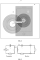
- FIG. 2 is a schematic diagram of a position deviation between a transmitter and a receiver according to an embodiment of this application.
- a position deviation s between the transmitter 10 and the receiver 20 may be understood as a deviation between positions of a center of the transmitter coil 104 in the transmitter 10 and a center of the receiver coil 201 in the receiver 20, for example, may be a horizontal distance between the center of the transmitter coil 104 in the transmitter 10 and the center of the receiver coil 201 in the receiver 20.
- the position deviation s between the transmitter 10 and the receiver 20 may alternatively be understood as a deviation between positions of a center of a target transmitter coil in the transmitter 10 and the center of the receiver coil 201 in the receiver 20.
- the target transmitter coil may be one or more transmitter coils in the transmitter 10 that are closest to the receiver coil 201 in the receiver 20.
- a mutual inductance is short for a coefficient of mutual induction, and may be used to represent magnitude of a phenomenon of mutual induction between the transmitter coil in the transmitter and the receiver coil in the receiver.
- the coupling factor and the mutual inductance can both be used to indicate a degree of coupling between the transmitter coil in the transmitter 10 and the receiver coil in the receiver 20.
- a newly defined parameter may also be used to indicate the degree of coupling between the transmitter coil in the transmitter 10 and the receiver coil in the receiver 20.
- the coupling factor K is used as an example for description in the embodiments of this application. It can be understood that in the embodiments of this application, the degree of coupling between the transmitter coil in the transmitter 10 and the receiver coil in the receiver 20 is not limited to being indicated by the coupling factor, but may be indicated by the mutual inductance or may be indicated by another newly defined parameter.
- An operating frequency is a frequency at which the transmitter transfers power to the receiver in the wireless charging system. Different power is transferred on a coupling coil at different operating frequencies. When the operating frequency is 1 2 ⁇ L p ⁇ L p , power transferred on the coupling coil is maximum.
- a voltage gain is a ratio of an output voltage of a receiver to an input voltage of a transmitter.
- the output voltage is a voltage value that is obtained after rectification by an AC/DC conversion module in the receiver
- the input voltage is a voltage value that is obtained after conversion by a DC/AC conversion module in the transmitter.
- the load-independent point is a point that is on a relationship curve between a voltage gain and an operating frequency and at which a change in an output load impedance of a receiver does not affect a voltage gain and an operating frequency of the wireless charging system.
- FIG. 3 shows an equivalent circuit model of a wireless charging system according to an embodiment of this application.
- the wireless charging system shown in FIG. 1 may be equivalent to a magnetic coupling structure model of the wireless charging system shown in FIG. 3 .
- An output voltage of a transmitter is U op
- an output current of the transmitter is I op
- a frequency of the output voltage and the output current is f op .
- C p is a series matching capacitance of the transmitter
- L p is a self-inductance applied when a transmitter coil in the transmitter transfers power to the receiver
- R p is an input resistance of the transmitter.
- C s is a series matching capacitance of the receiver
- L s is a self-inductance applied when a receiver coil in the receiver receives the power transferred by the transmitter
- R s is a resistance of the receiver
- i s is a current on the coil of the receiver
- Z L is a load impedance.
- i L and u L are a load current and a load voltage, respectively.
- K is a coupling factor between the coil of the transmitter and the coil of the receiver.
- the second oscillation circuit is configured to receive the power transferred by the first oscillation circuit, and transfer the power to an AC/DC conversion module.
- the series matching capacitor of the transmitter may be referred to as a first series matching capacitor
- the series matching capacitor of the receiver may be referred to as a second series matching capacitor.
- FIG. 4 is a schematic diagram of a relationship between a voltage gain and an operating frequency according to an embodiment of this application.
- a set of X- ⁇ curves corresponding to a load impedance Z L whose values are Z1, Z2, and Z3 are respectively drawn, where Z1, Z2, and Z3 are different values.
- the set of X- ⁇ curves corresponding to Z1, Z2, and Z3 intersect at a same point.
- an operating frequency is ⁇ 0
- a voltage gain is X0
- ( ⁇ 0, X0) may be referred to as a load-independent point.
- the load-independent point is an inherent feature of the wireless charging system.
- the voltage gain is invariably X0 regardless of a value of the output load impedance Z L of the receiver.
- the following provides specific calculation of the voltage gain X0 and the operating frequency ⁇ 0 of the load-independent point of the wireless charging system.
- FIG. 5 shows another equivalent circuit model of a wireless charging system according to an embodiment of this application.
- L kp is a transformer primary leakage inductance
- L ks is a transformer secondary leakage inductance
- L m is a transformer primary excitation inductance.
- ⁇ 0 and X0 may be expressed as formula (3) and formula (6), respectively.
- a load-independent point is related to a coupling factor.
- the coupling factor is a fixed value. Therefore, when relative displacement of the transmitter and the receiver is constant, the load-independent point is also definite.
- FIG. 6 is a schematic diagram of another relationship between a voltage gain and an operating frequency according to an embodiment of this application.
- Const > 0, and values of the coupling factor K are K0, K1, and K2, respectively, corresponding load-independent points are ( ⁇ 0, X0), ( ⁇ 1, X1), and ( ⁇ 2, X2), respectively.
- Position deviations, corresponding to the coupling factors K0, K1, and K2, between the transmitter and the receiver are s0, s1, and s2, respectively, where s0 > s1 > s2. It can be learned with reference to FIG.
- FIG. 7 is a schematic diagram of still another relationship between a voltage gain and an operating frequency according to an embodiment of this application.
- Const 0 (not according to the claims) and Const ⁇ 0 (according to the claims), wireless charging methods in which a wireless charging system operates at a load-independent point are designed, respectively. Descriptions are separately given below.
- a process of adjusting a wireless charging system to operate at a load-independent point is as follows:
- a voltage gain X at a load-independent point and an operating frequency ⁇ change with a coupling factor.
- a primary excitation inductance L m is related to a coupling factor, and L m is unknown. Therefore, when Const ⁇ 0, for the wireless charging system, the load-independent point cannot be directly obtained through calculation.
- a mapping relationship between a coupling factor, Const, and a load-independent point may be pre-stored, to obtain a first mapping table.
- the wireless charging system may first determine the coupling factor between the transmitter and the receiver based on a position deviation between the transmitter and the receiver, and query the first mapping table, to obtain a load-independent point corresponding to the current coupling factor. In addition, the wireless charging system is adjusted to operate at this load-independent point.
- the wireless charging system needs to be set to operate at the load-independent point when transferring power.
- a voltage gain between an output voltage of the receiver and an input voltage of the transmitter may be set to be invariably a voltage gain X0 at the load-independent point, and an operating frequency at which the transmitter transfers power to the receiver is the operating frequency ⁇ 0 at the load-independent point.
- a voltage needs to be regulated.
- a voltage regulation module may be disposed in the transmitter, and is configured to regulate the input voltage of the transmitter to set the voltage gain to the voltage gain X0 at the load-independent point.
- a voltage regulation module may be disposed in the receiver, and is configured to regulate the output voltage of the receiver to set the voltage gain to the voltage gain X0 at the load-independent point.
- the operating frequency is regulated to the operating frequency ⁇ 0 at the load-independent point through closed-loop frequency conversion.
- the voltage regulation module may be disposed in the transmitter, or the voltage regulation module may be disposed in the receiver.
- Const 0, several embodiments of the methods for regulating a wireless charging system to operate at a load-independent point are provided in the embodiments of this application based on the foregoing main inventive principle and the foregoing two manners.
- an embodiment of this application provides a wireless charging system.
- circuit parameters L p , C p , L s , and C s of a transmitter and a receiver can allow the voltage gain at the load-independent point not to change with the coupling factor.
- a position deviation slightly affects L p and L s .
- the condition that k meets 0.8 ⁇ k ⁇ 1.2 is not limited. For example, it may also be 0.7 ⁇ k ⁇ 1.3.
- the range may be determined based on a design precision requirement of the wireless charging system. This is not limited in this application.
- FIG. 8 is a schematic architectural diagram of another wireless charging system according to an embodiment of this application.
- a transmitter 10 may include a DC power source 101, a DC/AC conversion module 102, a series matching capacitor (whose capacitance is C p ) 103, a transmitter coil 104, and a control module 105.
- a receiver 20 may include a receiver coil 201, a series matching capacitor (whose capacitance is C s ) 202, an AC/DC conversion module 203, a voltage regulator module 204, a output load 205, a modulation module 206, and a control module 207.
- the foregoing modules refer to the architecture of the wireless charging system described in FIG. 1 . Details are not described herein again.
- a voltage regulation module 106 is further disposed in the transmitter, and is configured to regulate an input voltage of the transmitter, to set a voltage gain to a voltage gain X0 at a load-independent point.
- the voltage regulation module 106 is configured to receive a direct current voltage that is output by the DC power source 101, and receive a control signal that is output by the control module 105, to regulate the direct current voltage and set the voltage gain to the voltage gain X0 at the load-independent point.
- the voltage regulation module 106 may be a DC/DC output voltage regulation module or a voltage adapter circuit.
- the voltage regulation module 106 is a first voltage regulation module.
- the receiver 20 further includes a battery management system (battery management system, BMS) 208.
- BMS battery management system
- the receiver 20 is further configured to receive an expected output voltage V_out_target sent by the BMS.
- the expected output voltage has the following two purposes: First, the V _out_target is used by the receiver to regulate an output voltage to the expected output voltage. Second, the expected output voltage V _out_target is further used by the transmitter to determine the input voltage of the transmitter as a first input voltage Vin_set based on the expected output voltage and the voltage gain X0 at the load-independent point, and regulate the input voltage to the first input voltage Vin_set by using the voltage regulation module in the transmitter. Descriptions are separately given below.
- V_out_target As shown in FIG. 8 , the receiver uses V_out_target as a reference for the voltage regulator module 204, and adds a preset increment to obtain a preset value of Vrect.
- the preset increment may be obtained through a table lookup, and is used to ensure normal operation of a related chip.
- the receiver obtains a current output voltage Vrect of a rectifier by detecting potential of a connection point of R1 and R2, obtains an error voltage based on the preset value of Vrect and the detected current Vrect, and sends the error voltage to the transmitter through in-band communication.
- the transmitter can regulate Vrect by changing an operating frequency ⁇ of power transfer between the transmitter and the receiver.
- the receiver can finally regulate Vrect to the preset value of Vrect by repeatedly using the foregoing error voltage feedback manner.
- the preset value of Vrect obtained based on the expected output voltage is referred to as a first output voltage below.
- the expected output voltage V_out_target is used by the transmitter to determine the input voltage of the transmitter as a first input voltage Vin_set based on the expected output voltage and the voltage gain X0 at the load-independent point, which is specifically based on the schematic structural diagram of the wireless charging system described in FIG. 8 .
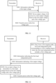
- FIG. 9 is a schematic flowchart of a wireless charging method according to an embodiment of this application.
- a voltage gain X0 at a load-independent point ( ⁇ 0, X0) of the wireless charging system is a first voltage gain.
- the voltage gain X0 at the load-independent point is the first voltage gain.
- the wireless charging method may include the following steps:
- a receiver sends, to a transmitter, information that indicates a first output voltage.
- the first output voltage is an expected output voltage of the receiver.
- the transmitter sets an input voltage of the transmitter to a first input voltage based on the first output voltage and a first voltage gain.
- the transmitter transfers power to the receiver at the first voltage gain.
- the transmitter transfers the power to the receiver at the first voltage gain
- the first voltage gain is the voltage gain at the load-independent point
- an operating frequency at which the transmitter transfers the power to the receiver is a first operating frequency
- the input voltage of the transmitter is the first input voltage
- the expected output voltage of the receiver is sent by a BMS to a control module 207.
- regulation of the input voltage of the transmitter to the first input voltage is also a closed-loop feedback regulation process.
- a specific process is as follows: The input voltage of the transmitter is gradually regulated based on the first input voltage. A change in the input voltage of the transmitter may cause an output voltage of the receiver to deviate from the first output voltage. A deviation of the output voltage of the receiver causes the receiver to start closed-loop feedback circuit regulation of the first output voltage again, to regulate the output voltage to the expected output voltage, causing the transmitter to regulate an operating frequency of power transfer.
- the input voltage of the transmitter is finally regulated to the first input voltage, the voltage gain is the voltage gain X0 at the load-independent point, and the operating frequency of the power transfer is exactly the operating frequency ⁇ 0 at the load-independent point.
- the input voltage of the transmitter is an output voltage of a voltage regulation module 106 in the transmitter.
- the output voltage of the receiver is an output voltage Vrect of the AC/DC conversion module 203 in the receiver.
- the voltage gain X0 at the load-independent point is the first voltage gain.
- the voltage gain at the load-independent point of the wireless charging system is constant.
- the first voltage gain X0 may be a positive number that meets 0.8 * L s / L p ⁇ X 0 ⁇ 1.2 * L s / L p .
- a voltage gain value at the load-independent point is set to C p / C s 1 + 20 % or C p / C s 1 ⁇ 20 % . It can be understood that in this embodiment of this application, an offset specified for the voltage gain is not limited.
- the first voltage gain may be set to C p / C s 1 + 30 % or C p / C s 1 ⁇ 30 % .
- the range may be determined based on a design precision requirement of the wireless charging system. This is not limited in this application.
- the voltage gain at the load-independent point is invariably C p / C s .
- the voltage gain is set to be within a range of 0.8 * L s / L p ⁇ X ⁇ 1.2 * L s / L p or within a range of 0.8 * C p / C s ⁇ X ⁇ 1.2 * C p / C s , so that the wireless charging system operates near the load-independent point, and the voltage gain is independent of a load impedance of the receiver. Therefore, regardless of a value of an output load impedance of the receiver, both an operating frequency and a voltage gain that are used when the transmitter transfers power to the receiver are fixed values.
- the output load impedance of the receiver does not affect a voltage gain between an output voltage of the receiver and an input voltage of the transmitter. Therefore, the output voltage of the receiver is constant, an output voltage jump caused by a load jump can be reduced, an electrical energy loss of a voltage regulator module can be reduced, and charging efficiency of the receiver can be improved.
- the first output voltage may be the expected output voltage of the BMS in the receiver.
- the expected output voltage of the BMS in the receiver may change.
- the expected output voltage of the BMS may be affected by factors such as a quantity of electricity of the receiver. For example, the voltage gain at the load-independent point is 1.1. If the receiver has a relatively small quantity of electricity (which may be lower than a threshold), the expected output voltage of the BMS in the receiver may be 9.9 V.
- the receiver feeds back a difference between a current output voltage and a specified output voltage to the transmitter through a closed-loop circuit.
- the transmitter regulates an operating frequency when receiving the voltage difference.
- An output voltage of the voltage regulator module in the receiver is regulated to 9.9 V through the foregoing closed-loop regulation process.
- the receiver sends the expected output voltage 9.9 V of the BMS to the transmitter, and the transmitter determines, through calculation based on the expected output voltage 9.9 V of the BMS and the voltage gain of 1.1, that the input voltage of the transmitter is 9 V. Therefore, the transmitter gradually regulates the input voltage of the transmitter by using the voltage regulation module, and a change in the input voltage of the transmitter causes the output voltage of the receiver to deviate from 9.9 V.
- the receiver detects that the output voltage of the receiver deviates from 9.9 V
- the receiver starts the closed-loop circuit to feed back the difference between the current output voltage and the specified output voltage to the transmitter, and the transmitter re-regulates the operating frequency based on the voltage difference.
- the input voltage of the transmitter is 9 V
- the output voltage of the receiver is 9.9 V
- the voltage gain is 1.1
- the operating frequency is exactly the operating frequency at the load-independent point.
- the expected output voltage of the BMS may be 5.5 V.
- the current output voltage of the receiver is still 9.9 V, and then the receiver may repeat the foregoing closed-loop circuit regulation process.
- the input voltage of the transmitter is finally adjusted to 5 V, the output voltage of the receiver is regulated to 5.5 V, the voltage gain is 1.1, and the operating frequency is exactly the operating frequency at the load-independent point.
- the wireless charging system When the wireless charging system performs power transfer at the load-independent point, if the receiver moves, a position deviation between the receiver and the transmitter changes, and then a coupling factor between an inductor coil of the transmitter and an inductor coil of the receiver changes. As shown in FIG. 7 , if the coupling factor applied before the receiver moves is K0, the wireless charging system operates at the load-independent point ( ⁇ 0, X0). If the coupling factor applied after the receiver moves is K1, the load-independent point of the wireless charging system becomes ( ⁇ 1, X0). After the receiver moves, as shown in FIG. 7 , a ⁇ -X curve 1 becomes a ⁇ -X curve 2.
- the receiver may perform the closed-loop circuit regulation process. For a specific process, refer to detailed descriptions in step S104. Details are not described herein again.
- the voltage gain is brought back to X0, the corresponding operating frequency is ⁇ 1, and the wireless charging system operates at the load-independent point ( ⁇ 1, X0) corresponding to the coupling factor K1.
- the first input voltage is obtained by dividing the first output voltage by the first voltage gain.
- the first voltage gain may be sent by the receiver to the transmitter.
- the receiver may obtain the first voltage gain through calculation based on C p and C s (or L s and L p ) and send the first voltage gain to the transmitter.
- the receiver may preset a voltage gain and send the voltage gain to the transmitter.
- the first voltage gain may be obtained by the receiver through calculation based on C p and C s (or L s and L p ), and the transmitter may receive in advance information sent by the receiver and indicating C s or information sent by the receiver and indicating L s .
- C s (L s ) and the first output voltage may be indicated by a same piece of information, or may be indicated by different pieces of information. This is not limited in this application.
- the voltage regulation module is disposed in the transmitter, and the transmitter regulates the voltage gain to the voltage gain at the load-independent point by regulating the input voltage, so that the wireless charging system finally operates at the load-independent point.
- the voltage regulation module may be disposed in the receiver, which is described in detail below.
- the wireless charging system operates near the load-independent point, so that the voltage gain is independent of a load impedance of the receiver. Therefore, regardless of a value of an output load impedance of the receiver, both an operating frequency and a voltage gain that are used when the transmitter transfers power to the receiver are fixed values. In other words, the output load impedance of the receiver does not affect a voltage gain between an output voltage of the receiver and an input voltage of the transmitter. Therefore, the output voltage of the receiver is constant, an output voltage jump caused by a load jump can be reduced, an electrical energy loss of a voltage regulator module can be reduced, and charging efficiency of the receiver can be improved.
- the voltage gain at the load-independent point is also unrelated to the coupling factor.
- the voltage gain at the load-independent point is invariably C p / C s .
- the operating frequency at which the wireless charging system performs power transfer may be regulated to the operating frequency at the load-independent point under an effect of a closed-loop circuit, so that the wireless charging system can operate at the load-independent point.
- FIG. 10 is a schematic structural diagram of still another wireless charging system according to an embodiment of this application.
- a transmitter 10 may include a DC power source 101, a DC/AC conversion module 102, a series matching capacitor (whose capacitance is Cp) 103, a transmitter coil 104, and a control module 105.
- a receiver 20 may include a receiver coil 201, a series matching capacitor (whose capacitance is C s ) 202, an AC/DC conversion module 203, a voltage regulator module 204, a output load 205, a modulation module 206, a control module 207, and a battery management system 208.
- the series matching capacitor 103 is a first series matching capacitor
- the series matching capacitor (whose capacitance is C s ) 202 is a second series matching capacitor.
- a voltage regulation module 209 is further disposed in the receiver, and is configured to regulate an output voltage of the receiver, to set a voltage gain to a voltage gain X0 at a load-independent point.
- the voltage regulation module 209 is configured to receive a voltage that is output by the AC/DC conversion module 203, and receive a control signal that is output by the control module 207, to regulate the voltage and set the voltage gain to the voltage gain X0 at the load-independent point.
- the voltage regulation module 209 is a second voltage regulation module.
- a process in which the receiver regulates the output voltage of the receiver to the first output voltage is also a closed-loop feedback regulation process.
- a specific process is as follows: The output voltage of the receiver is gradually regulated based on the first output voltage.
- the receiver obtains a voltage difference based on calculation of the first output voltage and the current output voltage of the voltage regulation module of the receiver, and sends the voltage difference to the transmitter through in-band communication.
- the transmitter regulates the operating frequency based on the voltage difference.
- the output voltage of the receiver is finally regulated to the first output voltage
- the voltage gain is the voltage gain X0 at the load-independent point
- the operating frequency of the power transfer is exactly the operating frequency ⁇ 0 at the load-independent point.
- FIG. 11 is a schematic flowchart of another wireless charging method according to an embodiment of this application.
- a voltage gain at a load-independent point ( ⁇ 0, X0) of the wireless charging system is a constant X0. Regardless of a value of a coupling factor, the voltage gain at the load-independent point is X0.
- the wireless charging method may include the following steps:
- the transmitter transfers the power to the receiver at the first voltage gain
- the first voltage gain is the voltage gain at the load-independent point
- an operating frequency at which the transmitter transfers the power to the receiver is a first operating frequency
- the output voltage of the receiver is the first output voltage
- the transmitter regulates an operating frequency of power transfer to the operating frequency at the load-independent point through closed-loop feedback regulation.
- the wireless charging system operates at the load-independent point.
- the first voltage gain X0 may be a positive number that meets 0.8 * L s / L p ⁇ X 0 ⁇ 1.2 * L s / L p .
- a voltage gain value at the load-independent point is set to C p / C s 1 + 20 % or C p / C s 1 ⁇ 20 % . It can be understood that in this embodiment of this application, an offset specified for the voltage gain is not limited.
- the first voltage gain may be set to C p / C s 1 + 30 % or C p / C s 1 ⁇ 30 % .
- the range may be determined based on a design precision requirement of the wireless charging system. This is not limited in this application.
- the transmitter may receive information sent by the receiver and indicating the first output voltage, and determine the input voltage of the transmitter as the first input voltage based on the first output voltage.
- the transmitter may determine the first input voltage based on a pre-stored second mapping table.
- the second mapping table includes at least one output voltage and an input voltage of the transmitter corresponding to each of the at least one output voltage.
- the transmitter is also required to include a voltage regulation module.
- the voltage regulation module refer to the voltage regulation module 106 in the transmitter in the embodiment described in FIG. 8 .
- the voltage regulation module is configured to regulate the input voltage of the transmitter to the first input voltage after the transmitter determines the input voltage of the transmitter as the first input voltage based on the first output voltage.
- the wireless charging system When the wireless charging system performs power transfer at the load-independent point, if the receiver moves, a position deviation between the receiver and the transmitter changes, and then a coupling factor between an inductor coil of the transmitter and an inductor coil of the receiver changes. As shown in FIG. 7 , if the coupling factor applied before the receiver moves is K0, the wireless charging system operates at the load-independent point ( ⁇ 0, X0). If the coupling factor applied after the receiver moves is K1, the load-independent point of the wireless charging system becomes ( ⁇ 1, X0). After the receiver moves, as shown in FIG. 7 , a ⁇ -X curve 1 becomes a ⁇ -X curve 2.
- the receiver may perform the closed-loop circuit regulation process. For a specific process, refer to detailed descriptions in step S104. Details are not described herein again.
- the voltage gain is brought back to X0, the corresponding operating frequency is ⁇ 1, and the wireless charging system operates at the load-independent point ( ⁇ 1, X0) corresponding to the coupling factor K1.
- the first output voltage is obtained by multiplying the first input voltage by the first voltage gain.
- the first voltage gain may be sent by the transmitter to the receiver.
- the transmitter may obtain the first voltage gain through calculation based on C p and C s (or L s and L p ) and send the first voltage gain to the receiver.
- the first voltage gain may be obtained by the transmitter through calculation based on C p and C s (or L s and L p ).
- the receiver may receive in advance information sent by the transmitter and indicating C p or information sent by the transmitter and indicating L p .
- C p (L p ) and the first input voltage may be indicated by a same piece of information, or may be indicated by different pieces of information. This is not limited in this application.
- the wireless charging system operates near the load-independent point, so that the voltage gain is independent of a load impedance of the receiver. Therefore, regardless of a value of an output load impedance of the receiver, both an operating frequency and a voltage gain that are used when the transmitter transfers power to the receiver are fixed values. In other words, the output load impedance of the receiver does not affect a voltage gain between an output voltage of the receiver and an input voltage of the transmitter. Therefore, the output voltage of the receiver is constant, an output voltage jump caused by a load jump can be reduced, an electrical energy loss of a voltage regulator module can be reduced, and charging efficiency of the receiver can be improved.
- the voltage gain at the load-independent point is also unrelated to the coupling factor.
- the voltage gain at the load-independent point is invariably C p / C s .
- the operating frequency at which the wireless charging system performs power transfer may be regulated to the operating frequency at the load-independent point under an effect of a closed-loop circuit, so that the wireless charging system can operate at the load-independent point.
- a capacitance and an inductance may be designed based on a desired voltage gain.
- the voltage gain of the wireless charging system is set to the voltage gain corresponding to the load-independent point, that is, the first voltage gain.
- the wireless charging system operates at the load-independent point.
- a change in an output resistance of the receiver does not affect the operating frequency of power transfer, and the change in the output resistance of the receiver does not cause a change in the voltage gain, either. Therefore, the output voltage of the receiver is constant, and an output voltage jump caused by an output resistance jump of the receiver is reduced, thereby reducing electrical energy consumed by the voltage regulator module and improving charging efficiency.
- Table 1 is an output voltage jump test result of a load jump at ( ⁇ 0, X0).
- the wireless charging system can also be designed to operate at the load-independent point.
- the methods for regulating a wireless charging system to operate at a load-independent point are separately provided in the embodiments of this application based on the foregoing two manners.
- FIG. 12 is a schematic flowchart of still another wireless charging method according to an embodiment of this application.
- a voltage gain X0 at a load-independent point ( ⁇ 0, X0) of the wireless charging system is related to a coupling factor.
- the wireless charging method may include the following steps:
- a receiver finds, from a first mapping table, a first load-independent point corresponding to a first coupling degree, where the first load-independent point includes a first voltage gain.
- the receiver sends, to a transmitter, information that indicates the first load-independent point.
- the receiver sends, to the transmitter, information that indicates a first output voltage.
- the transmitter sets an input voltage of the transmitter to a first input voltage based on the first output voltage and a first voltage gain.
- the transmitter transfers power to the receiver at the first voltage gain.
- the transmitter transfers the power to the receiver at the first voltage gain
- the first voltage gain is the voltage gain at the load-independent point
- an operating frequency at which the transmitter transfers the power to the receiver is a first operating frequency
- the input voltage of the transmitter is the first input voltage
- the receiver may pre-store the first mapping table, the first mapping table may include at least one coupling degree and a load-independent point corresponding to each of the at least one coupling degree, and the load-independent point is a combination of a voltage gain and an operating frequency.
- a voltage gain in the load-independent point corresponding to the coupling degree is independent of an output load of the receiver.
- the foregoing coupling degree may be a coupling factor or a mutual inductance. The coupling factor is described as an example below.
- the first mapping table may have two forms depending on whether Const is known. Descriptions are separately given below.
- Const corresponding to the transmitter and the receiver is Const 0.
- a coupling factor Ku corresponding when the position deviation s is su (u 0, 1, 2, ..., n)
- a load-independent point (Xu, ⁇ u) may be tested and stored in advance, where n and u both are natural numbers.
- the receiver may pre-store the foregoing first mapping table.
- the receiver finds a corresponding load-independent point based on a detected position deviation between the receiver and the transmitter, and then, sends the found load-independent point to the transmitter. For example, if the receiver detects that a current position deviation between the receiver and the transmitter is s2, the receiver determines, through a table lookup based on the foregoing pre-stored first mapping table, that a coupling factor is K2 and a load-independent point is (X2, ⁇ 2).
- Table 3 is a schematic diagram of another first mapping table according to an embodiment of this application.
- Const corresponding to the transmitter and the receiver is Const 0.
- the receiver may pre-store the foregoing first mapping table.
- the receiver finds a corresponding voltage gain at a load-independent point based on a detected position deviation between the receiver and the transmitter, and then, sends the found voltage gain at the load-independent point to the transmitter. For example, if the receiver detects that a current position deviation between the receiver and the transmitter is s2, the receiver determines, through a table lookup based on the foregoing pre-stored first mapping table, that a coupling factor is K2 and a voltage gain at a load-independent point is X2.
- the receiver or the transmitter can alternatively calculate the operating frequency at the load-independent point based on formula (3) and formula (6).
- a value of Const may be changed at fixed steps to test different coupling factors under different Const and load-independent points corresponding to the coupling factors.
- Load-independent points corresponding to different Const and coupling factors K may be pre-stored.
- Table 4 is an example of still another first mapping table according to an embodiment of this application.
- the receiver may pre-store the foregoing first mapping table.
- the receiver may first obtain L p and C p of the transmitter, and obtain Const through calculation.
- the receiver finds a corresponding load-independent point based on Const obtained through calculation and a detected position deviation between the receiver and the transmitter, and then, sends the found load-independent point to the transmitter. For example, if Const obtained by the receiver through calculation is Const 1, and the receiver detects that a current position deviation between the receiver and the transmitter is s2, the receiver determines, through a table lookup based on the foregoing pre-stored first mapping table, that the load-independent point is (X12, ⁇ 12).
- the receiver may alternatively pre-store only the voltage gain X at the load-independent point in the first mapping table.
- Table 5 is a schematic diagram of yet another first mapping table according to an embodiment of this application.
- the receiver may pre-store the foregoing first mapping table.
- the receiver may first obtain L p and C p of the transmitter, and obtain Const through calculation.
- the receiver finds a corresponding voltage gain at a load-independent point based on Const obtained through calculation and a detected position deviation between the receiver and the transmitter, and then, sends the found voltage gain at the load-independent point to the transmitter. For example, if Const obtained by the receiver through calculation is Const 1, and the receiver detects that a current position deviation between the receiver and the transmitter is s2, the receiver determines, through a table lookup based on the foregoing pre-stored first mapping table, that the voltage gain at the load-independent point is X12.
- the receiver is usually a mobile terminal and has very high data storage and processing capabilities
- the first mapping table is stored in the receiver, load on the transmitter for data processing and storage can be reduced, a table lookup speed can be accelerated, and a delay for regulating a load-independent point can be reduced.
- the foregoing first mapping table may be alternatively stored in the transmitter.
- the transmitter can directly obtain the load-independent point through a table lookup, and the load-independent point does not need to be sent by using the receiver. In-band communication may be reduced, and signaling overheads may be reduced.
- the voltage gain may be set to the voltage gain X0 at the load-independent point plus or minus an offset.
- the voltage gain is set to the first voltage gain X0, and the first voltage gain X0 may be a positive number that meets 0.8 * L s / L p ⁇ X 0 ⁇ 1.2 * L s / L p .
- a voltage gain value at the load-independent point is set to C p / C s 1 + 20 % or C p / C s 1 ⁇ 20 % .
- an offset specified for the voltage gain is not limited.
- the first voltage gain may be set to C p / C s 1 + 30 % or C p / C s 1 ⁇ 30 % .
- the range may be determined based on a design precision requirement of the wireless charging system. This is not limited in this application.
- the load-independent point is found from the first mapping table by using the coupling degree.
- the wireless charging system may be set to operate at a load-independent point by setting a voltage gain to a voltage gain at the load-independent point, so that the voltage gain is independent of a load impedance of the receiver. Therefore, regardless of a value of an output load impedance of the receiver, both an operating frequency and a voltage gain that are used when the transmitter transfers power to the receiver are fixed values. In other words, the output load impedance of the receiver does not affect a voltage gain between an output voltage of the receiver and an input voltage of the transmitter.
- the output voltage of the receiver is constant, an output voltage jump caused by a load jump can be reduced, an electrical energy loss of a voltage regulator module can be reduced, and charging efficiency of the receiver can be improved.
- Circuit parameters of the transmitter and the receiver do not need to be limited, and generality of the transmitter and the receiver is improved.
- the wireless charging system can be set at the load-independent point.
- the transmitter or the receiver that has any circuit parameter can operate at the load-independent point. Therefore, the generality of the transmitter and the receiver can be improved.
- the voltage regulation module is disposed in the transmitter, and the transmitter regulates the voltage gain to the voltage gain at the load-independent point by regulating the input voltage, so that the wireless charging system finally operates at the load-independent point.
- the voltage regulation module may be disposed in the receiver, which is described in detail below.
- FIG. 13 is a schematic flowchart of yet another wireless charging method according to an embodiment of this application.
- a voltage gain X0 at a load-independent point ( ⁇ 0, X0) of the wireless charging system is related to a coupling factor.
- the wireless charging method may include the following steps:
- the receiver may pre-store the first mapping table, the first mapping table may include at least one coupling degree and a load-independent point corresponding to each of the at least one coupling degree, and the load-independent point is a combination of a voltage gain and an operating frequency.
- a voltage gain in the load-independent point corresponding to the coupling degree is independent of an output load of the receiver.
- the foregoing coupling degree may be a coupling factor or a mutual inductance. The mutual inductance is used as an example below.
- mapping table For description of the first mapping table, refer to the embodiment described in FIG. 12 . Details are not described herein again.
- a performing sequence of step S401 and step S402 is not limited.
- the transmitter may receive information sent by the receiver and indicating the first output voltage, and determine the input voltage of the transmitter as the first input voltage based on the first output voltage.
- the transmitter may determine the first input voltage based on a pre-stored second mapping table.
- the second mapping table includes at least one output voltage and an input voltage of the transmitter corresponding to each of the at least one output voltage.
- the transmitter is also required to include a voltage regulation module.
- the voltage regulation module refer to the voltage regulation module 106 in the transmitter in the embodiment described in FIG. 8 .
- the voltage regulation module is configured to regulate the input voltage of the transmitter to the first input voltage after the transmitter determines the input voltage of the transmitter as the first input voltage based on the first output voltage.
- the wireless charging system When the wireless charging system performs power transfer at the load-independent point, if the receiver moves, the coupling factor changes, and the voltage gain and the operating frequency at the load-independent point of the wireless charging system also change.
- the load-independent point needs to be determined again, and the wireless charging system is regulated to operate at the load-independent point, that is, steps S401 to S404 are repeated.
- the load-independent point is found from the first mapping table by using the coupling degree.
- the wireless charging system may be set to operate at a load-independent point by setting a voltage gain to a voltage gain at the load-independent point, so that the voltage gain is independent of a load impedance of the receiver. Therefore, regardless of a value of an output load impedance of the receiver, both an operating frequency and a voltage gain that are used when the transmitter transfers power to the receiver are fixed values. In other words, the output load impedance of the receiver does not affect a voltage gain between an output voltage of the receiver and an input voltage of the transmitter.
- the output voltage of the receiver is constant, an output voltage jump caused by a load jump can be reduced, an electrical energy loss of a voltage regulator module can be reduced, and charging efficiency of the receiver can be improved.
- Circuit parameters of the transmitter and the receiver do not need to be limited, and generality of the transmitter and the receiver is improved.
- the wireless charging system is set at the load-independent point.
- a change in an output resistance of the receiver does not affect the operating frequency of power transfer, and the change in the output resistance of the receiver does not cause a change in the voltage gain either. Therefore, the output voltage of the receiver is constant, and an output voltage jump caused by an output resistance jump of the receiver is reduced, thereby reducing electrical energy consumed by the voltage regulator module and improving electrical energy conversion efficiency.
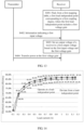
- FIG. 14 shows a test result of electrical energy conversion efficiency according to an embodiment of this application.
- a test curve of electrical energy conversion efficiency shown in FIG. 14 is a test result produced when a center of a transmitter coil in a transmitter directly faces a center of a receiver coil in a receiver, that is, when a position deviation is 0.
- the electrical energy conversion efficiency may be understood as a ratio of electrical energy that is output by the transmitter and electrical energy in the receiver that is used to supply power to a load.
- electrical energy conversion efficiency generated when a wireless charging system operates at a load-independent point is greater than electrical energy conversion efficiency generated when the wireless charging system deviates from the load-independent point. Therefore, when there is no position deviation between the transmitter and the receiver, the wireless charging system is set to operate at the load-independent point, and the electrical energy conversion efficiency of the wireless charging system can be improved.
- FIG. 15 shows another test result of electrical energy conversion efficiency according to an embodiment of this application.
- a test curve of electrical energy conversion efficiency shown in FIG. 15 is a test result produced when a center of a transmitter coil in a transmitter horizontally deviates from a center of a receiver coil in a receiver by 10 mm, that is, when a position deviation is 10 mm.
- electrical energy conversion efficiency generated when a wireless charging system operates at a load-independent point is greater than electrical energy conversion efficiency generated when the wireless charging system deviates from the load-independent point. Therefore, when there is a position deviation between the transmitter and the receiver, the wireless charging system is set to operate at the load-independent point, and the electrical energy conversion efficiency of the wireless charging system can be improved.
- a phase of an output voltage of a DC/AC conversion module in the transmitter is the same as a phase of an input voltage of an AC/DC conversion module in the receiver.
- the phase of the input voltage of the AC/DC conversion module in the receiver is also the same as a phase of an input current of the AC/DC conversion module in the receiver.
- the AC/DC conversion module in the receiver is implemented by using a rectifier diode circuit
- a diode has a zero current turn-off property.
- the zero current turn-off property of the diode can reduce electromagnetic interference and improve rectifier efficiency.
- FIG. 16 is a schematic diagram of a test of a voltage and a current according to an embodiment of this application.
- an output voltage of a DC/AC conversion module in a transmitter is V1
- an output current of the DC/AC conversion module in the transmitter is I1
- an input voltage of an AC/DC conversion module in a receiver is V2
- an input current of the AC/DC conversion module in the receiver is I2, where phases of V1 and V2 are the same, and phases of V2 and I2 are the same.
- the AC/DC conversion module in the receiver uses a diode circuit for rectification, where the diode has a zero current turn-off property. The zero current turn-off property of the diode can reduce electromagnetic interference and improve rectifier efficiency.
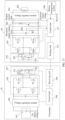
- FIG. 17 is a schematic structural diagram of a wireless charging system 100 according to an embodiment of this application.
- the wireless charging system 100 includes a transmitter 10 and a receiver 20.
- k is 1, and X is C p / C s or L s / L p .
- the transmitter 10 further includes a receiving unit 109, and that a control unit 108 sets a voltage gain between an output voltage of the receiver 20 and an input voltage of the transmitter 10 to a first voltage gain includes:
- the transmitter 10 may include a voltage regulation module 106. That the control unit 108 sets the input voltage of the transmitter 10 to a first input voltage based on the first output voltage and the first voltage gain includes: the control unit 108 controls, based on the first output voltage and the first voltage gain, the voltage regulation module 106 to set the input voltage of the transmitter 10 to the first input voltage.
- the receiving unit 109 is further configured to receive information sent by the receiver 20 and indicating C s and/or information sent by the receiver 20 and indicating L s , where C s and L s are used by the transmitter 10 to determine the first voltage gain; and/or the receiving unit 109 is configured to receive information sent by the receiver 20 and indicating the first voltage gain.
- the receiver 20 further includes a sending unit 212 and a control unit 211, where
- the transmitter 10 may further include a DC power source 101 and a DC/AC conversion module 102.
- the receiver 20 may include an AC/DC conversion module 203, a voltage regulator module 204, a output load 205, a modulation module 206, and a battery management system 208.
- control unit 108 may be implemented by the control module 105 in the embodiment described in FIG. 8 .
- the control unit 211 may be implemented by the control module 207 in the embodiment described in FIG. 8 .
- the control unit 108 may further have another function of the control module 105.
- the control unit 211 may further have another function of the control module 207.
- Functions of the control unit 108, the receiving unit 109, the control unit 211, and the sending unit 212 may correspond to the corresponding descriptions of the wireless charging method embodiment shown in FIG. 9 . Details are not described herein again.
- control unit 108 is configured to find, from a first mapping table, a first load-independent point corresponding to a first coupling degree;
- the receiving unit 109 is further configured to receive information sent by the receiver 20 and indicating C s and/or information sent by the receiver 20 and indicating L s , where C s and L s are used by the transmitter 10 to determine the first voltage gain; and/or the transmitter 10 is configured to receive information sent by the receiver 20 and indicating the first voltage gain.
- the sending unit 212 is configured to send, to the transmitter 10, information that indicates a first output voltage, where the first output voltage is an expected output voltage of the receiver 20; and the first output voltage is used by the transmitter 10 to set an input voltage of the transmitter 10 to a first input voltage based on the first output voltage and the first voltage gain.
- the first voltage gain is included in a first load-independent point corresponding to a first coupling degree and found by the transmitter 10 from a first mapping table; or the first voltage gain is included in a first load-independent point corresponding to a first coupling degree and found by the receiver 20 from a first mapping table; and the first load-independent point is added to information indicating the first load-independent point, and then sent by the receiver 20 to the transmitter 10.
- the first coupling degree is a degree of coupling between the transmitter coil 104 in the transmitter 10 and the receiver coil 201 in the receiver 20;
- the first mapping table includes at least one coupling degree and a load-independent point corresponding to each of the at least one coupling degree, and the load-independent point is a combination of a voltage gain and an operating frequency; and at an operating frequency in a load-independent point corresponding to each coupling degree, a voltage gain in the load-independent point corresponding to the coupling degree is independent of an output load of the receiver.
- the control unit 211 is configured to control the second oscillation circuit to receive the power transferred by the transmitter 10 at the first voltage gain.
- control unit 108 may be implemented by the control module 105 in the embodiment described in FIG. 8 .
- the control unit 211 may be implemented by the control module 207 in the embodiment described in FIG. 8 .
- the control unit 108 may be a controller 30 in the embodiment described in FIG. 19 .
- the control unit 211 may be a controller 40 in the embodiment described in FIG. 19 .
- the control unit 108 may further have another function of the control module 105.
- the control unit 211 may further have another function of the control module 207.
- Functions of the control unit 108, the receiving unit 109, the control unit 211, and the sending unit 212 may correspond to the corresponding descriptions of the wireless charging method embodiment shown in FIG. 12 . Details are not described herein again.
- FIG. 18 is a schematic structural diagram of another wireless charging system 100 according to an embodiment of this application.
- the wireless charging system 100 includes a transmitter 10 and a receiver 20.
- the receiver 20 further includes a control unit 211, where
- k is 1, and X is C p / C s or L s / L p .
- the receiver 20 further includes a receiving unit 212, and that the control unit 211 sets a voltage gain between an output voltage of the receiver 20 and an input voltage of the transmitter 10 to a first voltage gain includes:
- the receiver 20 may include a voltage regulation module 209. That the control unit 211 sets the output voltage of the receiver 20 to a first output voltage based on the first input voltage and the first voltage gain includes: the control unit 211 controls, based on the first input voltage and the first voltage gain, the voltage regulation module 209 to set the output voltage of the receiver 10 to the first output voltage.
- the receiving unit 212 is further configured to receive information sent by the transmitter 10 and indicating C p and/or information sent by the transmitter 10 and indicating L p , where C p and L p are used by the receiver 20 to determine the first voltage gain; and/or the receiving unit 212 is further configured to receive information sent by the transmitter 10 and indicating the first voltage gain.
- the transmitter 10 may further include a DC power source 101 and a DC/AC conversion module 102.
- the receiver 20 may further include an AC/DC conversion module 203, a voltage regulator module 204, a output load 205, a modulation module 206, and a battery management system 208.
- control unit 109 may be implemented by the control module 105 in the embodiment described in FIG. 10 .
- the control unit 211 may be implemented by the control module 207 in the embodiment described in FIG. 10 .
- the control unit 109 may be a controller 30 in the embodiment described in FIG. 19 .
- the control unit 211 may be a controller 40 in the embodiment described in FIG. 19 .
- the control unit 109 may further have another function of the control module 105.
- control unit 211 may further have another function of the control module 207.
- Functions of the control unit 109, the sending unit 108, the control unit 211, and the receiving unit 212 may correspond to the corresponding descriptions of the wireless charging method embodiment shown in FIG. 11 . Details are not described herein again.
- the sending unit 108 is configured to send, to the receiver 20, information that indicates a first input voltage, where the first input voltage is an input voltage of the transmitter 10; and the first input voltage is used by the receiver 20 to set an output voltage of the receiver 20 to a first output voltage based on the first input voltage and the first voltage gain.
- the first voltage gain is included in a first load-independent point corresponding to a first coupling degree and found by the transmitter 10 from a first mapping table; or the first voltage gain is included in a first load-independent point corresponding to a first coupling degree and found by the receiver 20 from a first mapping table; and the first load-independent point is added to information indicating the first load-independent point, and then sent by the receiver to the transmitter 10.
- the first coupling degree is a degree of coupling between the transmitter coil 104 in the transmitter 10 and the receiver coil 201 in the receiver 20;
- the first mapping table includes at least one coupling degree and a load-independent point corresponding to each of the at least one coupling degree, and the load-independent point is a combination of a voltage gain and an operating frequency; and at an operating frequency in a load-independent point corresponding to each coupling degree, a voltage gain in the load-independent point corresponding to the coupling degree is independent of an output load of the receiver; and the control unit 109 is further configured to control the first oscillation circuit 107 to transfer the power to the receiver 20 at the first voltage gain.
- control unit 211 is configured to find, from a first mapping table, a first load-independent point corresponding to a first coupling degree;
- the receiving unit 212 is further configured to receive information sent by the transmitter 10 and indicating C p and/or information sent by the transmitter 10 and indicating L p , where C p and L p are used by the receiver 20 to determine the first voltage gain; and/or receiving, by the receiver 20, information sent by the transmitter 10 and indicating the first voltage gain.
- control unit 109 may be implemented by the control module 105 in the embodiment described in FIG. 10 .
- the control unit 211 may be implemented by the control module 207 in the embodiment described in FIG. 10 .
- the control unit 108 may further have another function of the control module 105.
- the control unit 211 may further have another function of the control module 207.
- Functions of the control unit 108, the receiving unit 109, the control unit 211, and the sending unit 212 may correspond to the corresponding descriptions of the wireless charging method embodiment shown in FIG. 13 . Details are not described herein again.
- FIG. 19 is a schematic structural diagram of still another wireless charging system 100 according to an embodiment of this application.
- the wireless charging system 100 includes a transmitter 10 and a receiver 20.
- the transmitter 10 further includes a controller 30, where the controller 30 includes: one or more processors 301, a memory 302, and a communications interface 303. These components may be connected by using a bus 304 or in another manner. A bus connection is used as an example in FIG. 19 .
- the communications interface 303 may be configured for communication between the transmitter 10 and another communications device, for example, the receiver 20.
- the transmitter 10 and the receiver 20 may be the transmitter 10 and the receiver 20 shown in FIG. 8 or FIG. 17 .
- the communications interface 303 may be an in-band communications interface in the wireless charging system. For detailed descriptions of in-band communication, refer to the embodiment described in FIG. 1 .
- the communications interface 303 may be an out-band (out-band) interface, for example, a Bluetooth communications interface, a Zigbee communications interface, or a WiFi communications interface, or may be extended to another communications interface. This is not limited in this embodiment of this application.
- the memory 302 is coupled to the processor 301, and is configured to store various software programs and/or a plurality of sets of instructions.
- the memory 302 may further store a data transmission program.
- the data transmission program may be used for communication with one or more additional devices, one or more transmitters, or one or more receivers.
- the memory 302 may be configured to store a program for implementing, on a side of the transmitter 10, the wireless charging method provided in one or more embodiments of this application.
- the wireless charging method provided in one or more embodiments of this application refer to the embodiments described in FIG. 9 and FIG. 12 .
- the processor 301 may be configured to read and execute a computer readable instruction. Specifically, the processor 301 may be configured to invoke the program stored in the memory 302, for example, the program for implementing, on the side of the transmitter 10, the wireless charging method provided in one or more embodiments of this application, and execute the instruction included in the program.
- the transmitter 10 shown in FIG. 19 is merely one implementation in the embodiments of this application. During actual application, the transmitter 10 may further include more or fewer components, and this is not limited herein.
- the receiver 20 further includes a controller 40, where the controller 40 includes: one or more processors 401, a memory 402, and a communications interface 403. These components may be connected by using a bus 404 or in another manner.
- a bus connection is used as an example in FIG. 19 .
- the communications interface 403 may be configured for communication between the receiver 20 and another communications device, for example, the transmitter 10.
- the transmitter 10 and the receiver 20 may be the transmitter 10 and the receiver 20 shown in FIG. 8 or FIG. 17 .
- the communications interface 403 may be an in-band communications interface in the wireless charging system. For detailed descriptions of in-band communication, refer to the embodiment described in FIG. 1 .
- the communications interface 403 may be an out-band (out-band) interface, for example, a Bluetooth communications interface, a Zigbee communications interface, or a WiFi communications interface, or may be extended to another communications interface. This is not limited in this embodiment of this application.
- the memory 402 is coupled to the processor 401, and is configured to store various software programs and/or a plurality of sets of instructions.
- the memory 402 may further store a data transmission program.
- the data transmission program may be used for communication with one or more additional devices, one or more transmitters, or one or more receivers.
- the memory 402 may be configured to store a program for implementing, on a side of the receiver 20, the wireless charging method provided in one or more embodiments of this application.
- the wireless charging method provided in one or more embodiments of this application refer to the embodiments described in FIG. 9 and FIG. 12 .
- the processor 401 may be configured to read and execute a computer readable instruction. Specifically, the processor 401 may be configured to invoke the program stored in the memory 402, for example, the program for implementing, on the side of the receiver 20, the wireless charging method provided in one or more embodiments of this application, and execute the instruction included in the program.
- the receiver 20 shown in FIG. 19 is merely one implementation in the embodiments of this application. During actual application, the receiver 20 may further include more or fewer components, and this is not limited herein.
- the receiver 20 may be a mobile phone, a tablet computer, a computer having a wireless transceiver function, a virtual reality terminal device, or an augmented reality terminal device.
- the receiver 20 may be a wireless charging electric vehicle, or white goods, for example, a no-tail television, a wireless charging soymilk maker, a wireless charging vacuum cleaning robot, or a multi-rotor drone.
- FIG. 20 is a schematic structural diagram of yet another wireless charging system 100 according to an embodiment of this application.
- the wireless charging system 100 includes a transmitter 10 and a receiver 20.
- the communications interface 503 may be configured for communication between the transmitter 10 and another communications device, for example, the receiver 20.
- the transmitter 10 and the receiver 20 may be the transmitter 10 and the receiver 20 shown in FIG. 10 or FIG. 18 .
- the communications interface 503 may be an in-band communications interface in the wireless charging system. For detailed descriptions of in-band communication, refer to the embodiment described in FIG. 1 .
- the communications interface 503 may be an out-band (out-band) interface, for example, a Bluetooth communications interface, a Zigbee communications interface, or a WiFi communications interface, or may be extended to another communications interface. This is not limited in this embodiment of this application.
- the memory 502 is coupled to the processor 501, and is configured to store various software programs and/or a plurality of sets of instructions.
- the memory 502 may further store a data transmission program.
- the data transmission program may be used for communication with one or more additional devices, one or more transmitters, or one or more receivers.
- the memory 502 may be configured to store a program for implementing, on a side of the transmitter 10, the wireless charging method provided in one or more embodiments of this application.
- the wireless charging method provided in one or more embodiments of this application refer to the embodiments described in FIG. 11 and FIG. 13 .
- the processor 501 may be configured to read and execute a computer readable instruction. Specifically, the processor 501 may be configured to invoke the program stored in the memory 502, for example, the program for implementing, on the side of the transmitter 10, the wireless charging method provided in one or more embodiments of this application, and execute the instruction included in the program.
- the transmitter 10 shown in FIG. 20 is merely one implementation in the embodiments of this application. During actual application, the transmitter 10 may further include more or fewer components, and this is not limited herein.
- the transmitter 10 may further include a DC power source 101 and a DC/AC conversion module 102.
- the receiver 20 may include an AC/DC conversion module 203, a voltage regulator module 204, a output load 205, a modulation module 206, and a battery management system 208.
- the receiver 20 further includes a controller 60, where the controller 60 includes: one or more processors 601, a memory 602, and a communications interface 603. These components may be connected by using a bus 604 or in another manner.
- a bus connection is used as an example in FIG. 20 .
- the communications interface 603 may be configured for communication between the receiver 20 and another communications device, for example, the transmitter 10.
- the transmitter 10 and the receiver 20 may be the transmitter 10 and the receiver 20 shown in FIG. 10 or FIG. 18 .
- the communications interface 603 may be an in-band communications interface in the wireless charging system. For detailed descriptions of in-band communication, refer to the embodiment described in FIG. 1 .
- the communications interface 603 may be an out-band (out-band) interface, for example, a Bluetooth communications interface, a Zigbee communications interface, or a WiFi communications interface, or may be extended to another communications interface. This is not limited in this embodiment of this application.
- the memory 602 is coupled to the processor 601, and is configured to store various software programs and/or a plurality of sets of instructions.
- the memory 602 may further store a data transmission program.
- the data transmission program may be used for communication with one or more additional devices, one or more transmitters, or one or more receivers.
- the memory 602 may be configured to store a program for implementing, on a side of the receiver 20, the wireless charging method provided in one or more embodiments of this application.
- the wireless charging method provided in one or more embodiments of this application refer to the embodiments described in FIG. 11 and FIG. 13 .
- the processor 601 may be configured to read and execute a computer readable instruction. Specifically, the processor 601 may be configured to invoke the program stored in the memory 602, for example, the program for implementing, on the side of the receiver 20, the wireless charging method provided in one or more embodiments of this application, and execute the instruction included in the program.
- the receiver 20 shown in FIG. 20 is merely one implementation in the embodiments of this application. During actual application, the receiver 20 may further include more or fewer components, and this is not limited herein.
- the transmitter 10 may further include a DC power source 101 and a DC/AC conversion module 102.
- the receiver 20 may include an AC/DC conversion module 203, a voltage regulator module 204, a output load 205, a modulation module 206, and a battery management system 208.
- the transmitter chip implements functions of the transmitter in the foregoing method embodiment.
- the transmitter chip sends information to another module (for example, a radio frequency module or an antenna) of the transmitter, and the information is sent to the receiver by using the another module of the transmitter.
- the transmitter chip may receive information from another module (for example, a radio frequency module or an antenna) of the transmitter, and the information is sent to the transmitter by the receiver.
- the receiver chip implements functions of the receiver in the foregoing method embodiment.
- the receiver chip sends information to another module (for example, a radio frequency module or an antenna) of the receiver, and the information is sent to the transmitter by using the another module of the receiver.
- the receiver chip may receive information from another module (for example, a radio frequency module or an antenna) of the receiver, and the information is sent to the transmitter by the receiver.
- the processor in the embodiments of this application may be a central processing unit (Central Processing Unit, CPU), or may be another general-purpose processor, a digital signal processor (Digital Signal Processor, DSP), an application-specific integrated circuit (Application Specific Integrated Circuit, ASIC), a field programmable gate array (Field Programmable Gate Array, FPGA) or another programmable logical device, a transistor logic device, a hardware component, or any combination thereof.
- the general-purpose processor may be a microprocessor or any conventional processor.
- the method steps in the embodiments of this application may be implemented by hardware, or may be implemented by a processor executing a software instruction.
- the software instruction may include a corresponding software module.
- the software module may be located in a random access memory (Random Access Memory, RAM), a flash memory, a read-only memory (Read-Only Memory, ROM), a programmable read-only memory (Programmable ROM, PROM), an erasable programmable read-only memory (Erasable PROM, EPROM), an electrically erasable programmable read-only memory (Electrically EPROM, EEPROM), a register, a hard disk, a removable hard disk, a CD-ROM, or a storage medium of any other form known in the art.
- RAM Random Access Memory
- ROM read-only memory
- PROM programmable read-only memory
- Erasable PROM Erasable PROM
- EPROM electrically erasable programmable read-only memory
- EEPROM Electrically
- a storage medium is coupled to a processor, so that the processor can read information from the storage medium or write information into the storage medium.
- the storage medium may be a component of the processor.
- the processor and the storage medium may be located in the ASIC.
- the ASIC may be located in a sending device or a receiving device.
- the processor and the storage medium may exist in the sending device or the receiving device as discrete components.
- All or some of the foregoing embodiments may be implemented by using software, hardware, firmware, or any combination thereof.
- the embodiments may be implemented completely or partially in a form of a computer program product.
- the computer program product includes one or more computer instructions.
- the computer may be a general-purpose computer, a dedicated computer, a computer network, or another programmable apparatus.
- the computer instructions may be stored in a computer readable storage medium or transmitted by using the computer readable storage medium.
- the computer instructions may be transmitted from a website, computer, server, or data center to another website, computer, server, or data center in a wired (for example, a coaxial cable, an optical fiber, or a digital subscriber line (DSL)) or wireless (for example, infrared, radio, or microwave) manner.
- the computer readable storage medium may be any usable medium accessible by a computer, or a data storage device, such as a server or a data center, integrating one or more usable media.
- the usable medium may be a magnetic medium (for example, a floppy disk, a hard disk, or a magnetic tape), an optical medium (for example, a DVD), a semiconductor medium (for example, a solid state disk (Solid State Disk, SSD)), or the like.
- a magnetic medium for example, a floppy disk, a hard disk, or a magnetic tape
- an optical medium for example, a DVD
- a semiconductor medium for example, a solid state disk (Solid State Disk, SSD)
- the program may be stored in the computer readable storage medium. When the program runs, the procedures of the foregoing method embodiments are performed.
- the foregoing storage medium includes: any medium that can store program code, such as a ROM, a random access memory RAM, a magnetic disk, or an optical disc.
Landscapes
- Engineering & Computer Science (AREA)
- Power Engineering (AREA)
- Computer Networks & Wireless Communication (AREA)
- Charge And Discharge Circuits For Batteries Or The Like (AREA)
- Near-Field Transmission Systems (AREA)
Claims (6)
- System zum drahtlosen Laden, wobei das System (100) zum drahtlosen Laden einen Sender (10) und einen Empfänger (20) umfasst; der Sender eine Senderspule (104) und einen ersten Reihenanpassungskondensator (103) umfasst, die Senderspule mit dem ersten Reihenanpassungskondensator in Reihe geschaltet ist, um einen ersten Schwingkreis zu bilden, und der erste Schwingkreis dazu konfiguriert ist, eine Leistung an den Empfänger zu übertragen; und der Empfänger eine Empfängerspule (201) und einen zweiten Reihenanpassungskondensator (202) umfasst, die Empfängerspule mit dem zweiten Reihenanpassungskondensator in Reihe geschaltet ist, um einen zweiten Schwingkreis zu bilden, und der zweite Schwingkreis dazu konfiguriert ist, die Leistung, die durch den ersten Schwingkreis übertragen wird, zu empfangen; unddas System zum drahtlosen Laden derart konfiguriert ist, dass während der Leistungsübertragung eine Sender-Selbstinduktivität Lp und eine Kapazität des ersten Reihenanpassungskondensators Cp beträgt; und eine Empfänger-Selbstinduktivität Ls und eine Kapazität des zweiten Reihenanpassungskondensators Cs beträgt, wobei
 eine Einheit des Systems zum drahtlosen Laden zu Folgendem konfiguriert ist: Speichern einer vorbestimmten Zuordnungstabelle, Erkennen einer Positionsabweichung zwischen dem Sender und dem Empfänger und Bestimmen einer ersten Spannungsverstärkung basierend auf der erkannten Positionsabweichung und der vorbestimmten Zuordnungstabelle, wobei die vorbestimmte Zuordnungstabelle eine Vielzahl von Positionsabweichungen zwischen dem Sender und dem Empfänger und für jede der Vielzahl von Positionsabweichungen zwischen dem Sender und dem Empfänger eine vorbestimmte lastunabhängige Spannungsverstärkung beinhaltet, und wobei die Einheit des Systems zum drahtlosen Laden der Empfänger oder der Sender ist; unddas System zum drahtlosen Laden ferner dazu konfiguriert ist, an einem lastunabhängigen Punkt betrieben zu werden, wenn eine Spannungsverstärkung zwischen einer Ausgangsspannung des Empfängers und einer Eingangsspannung des Senders die erste Spannungsverstärkung ist; der lastunabhängige Punkt durch eine erste Betriebsfrequenz und die erste Spannungsverstärkung bestimmt wird; und bei der ersten Betriebsfrequenz die erste Spannungsverstärkung unabhängig von einer Ausgangslast des Empfängers ist.
 - System zum drahtlosen Laden nach Anspruch 1, wobei der Sender ferner ein erstes Spannungsregelungsmodul (106) umfasst, wobei das erste Spannungsregelungsmodul mit dem ersten Schwingkreis parallel geschaltet ist; und
das erste Spannungsregelungsmodul dazu konfiguriert ist, die Spannungsverstärkung zwischen der Ausgangsspannung des Empfängers und der Eingangsspannung des Senders auf die erste Spannungsverstärkung durch Regeln der Eingangsspannung des Senders einzustellen. - System zum drahtlosen Laden nach Anspruch 1 oder 2, wobei der Empfänger ferner ein zweites Spannungsregelungsmodul (209) umfasst, wobei das zweite Spannungsregelungsmodul mit dem zweiten Schwingkreis parallel geschaltet ist; und
das zweite Spannungsregelungsmodul dazu konfiguriert ist, die Spannungsverstärkung zwischen der Ausgangsspannung des Empfängers und der Eingangsspannung des Senders auf die erste Spannungsverstärkung durch Regeln der Ausgangsspannung des Empfängers einzustellen. - Verfahren zum Laden basierend auf einem System zum drahtlosen Laden, wobei das System (100) zum drahtlosen Laden einen Sender (10) und einen Empfänger (20) umfasst; der Sender eine Senderspule (104) und einen ersten Reihenanpassungskondensator (103) umfasst, die Senderspule mit dem ersten Reihenanpassungskondensator in Reihe geschaltet ist, um einen ersten Schwingkreis zu bilden, und der erste Schwingkreis dazu konfiguriert ist, eine Leistung an den Empfänger zu übertragen; der Empfänger eine Empfängerspule (201) und einen zweiten Reihenanpassungskondensator (202) umfasst, die Empfängerspule mit dem zweiten Reihenanpassungskondensator in Reihe geschaltet ist, um einen zweiten Schwingkreis zu bilden, und der zweite Schwingkreis dazu konfiguriert ist, die Leistung, die durch den ersten Schwingkreis übertragen wird, zu empfangen; eine Selbstinduktivität, die angewendet wird, wenn die Senderspule die Leistung an den Empfänger überträgt, Lp ist und eine Kapazität des ersten Reihenanpassungskondensators Cp ist; eine Selbstinduktivität, die angewendet wird, wenn die Empfängerspule die Leistung, die durch den ersten Schwingkreis übertragen wird, empfängt, Ls ist und eine Kapazität des zweiten Reihenanpassungskondensators Cs ist, wobei
 Speichern, durch eine Einheit des Systems zum drahtlosen Laden, einer vorbestimmten Zuordnungstabelle, wobei die Einheit des Systems zum drahtlosen Laden der Empfänger oder der Sender ist; Erkennen, durch die Einheit des Systems zum drahtlosen Laden, einer Positionsabweichung zwischen dem Sender und dem Empfänger; Bestimmen, durch die Einheit des Systems zum drahtlosen Laden, einer ersten Spannungsverstärkung basierend auf der erkannten Positionsabweichung und der vorbestimmten Zuordnungstabelle, wobei die vorbestimmte Zuordnungstabelle eine Vielzahl von Positionsabweichungen zwischen dem Sender und dem Empfänger und für jede der Vielzahl von Positionsabweichungen zwischen dem Sender und dem Empfänger eine vorbestimmte lastunabhängige Spannungsverstärkung beinhaltet;Einstellen, durch den Sender, einer Spannungsverstärkung zwischen einer Ausgangsspannung des Empfängers und einer Eingangsspannung des Senders auf die erste Spannungsverstärkung, wobei, wenn die Spannungsverstärkung zwischen der Ausgangsspannung des Empfängers und der Eingangsspannung des Senders die erste Spannungsverstärkung ist, das System zum drahtlosen Laden an einem lastunabhängigen Punkt betrieben wird; der lastunabhängige Punkt durch eine erste Betriebsfrequenz und die erste Spannungsverstärkung bestimmt wird; und bei der ersten Betriebsfrequenz die erste Spannungsverstärkung unabhängig von einer Ausgangslast des Empfängers ist; undÜbertragen, durch den Sender, der Leistung an den Empfänger bei der ersten Spannungsverstärkung.
 - Verfahren nach Anspruch 4, wobei das Einstellen, durch den Sender, einer Spannungsverstärkung zwischen einer Ausgangsspannung des Empfängers und einer Eingangsspannung des Senders auf die erste Spannungsverstärkung Folgendes umfasst:Empfangen, durch den Sender, von Informationen, die durch den Empfänger gesendet werden und eine erste Ausgangsspannung angeben, wobei die erste Ausgangsspannung eine erwartete Ausgangsspannung des Empfängers ist; undEinstellen, durch den Sender, der Eingangsspannung des Senders auf eine erste Eingangsspannung basierend auf der ersten Ausgangsspannung und der ersten Spannungsverstärkung.
- Verfahren nach Anspruch 4 oder 5, wobei das Verfahren vor dem Einstellen, durch den Sender, einer Spannungsverstärkung zwischen einer Ausgangsspannung des Empfängers und einer Eingangsspannung des Senders auf die erste Spannungsverstärkung ferner Folgendes umfasst:
Empfangen, durch den Sender, von Informationen, die durch den Empfänger gesendet werden und die erste Spannungsverstärkung angeben.
Applications Claiming Priority (2)
| Application Number | Priority Date | Filing Date | Title |
|---|---|---|---|
| CN201711178938.2A CN107834710B (zh) | 2017-11-21 | 2017-11-21 | 无线充电方法、设备及无线充电系统 |
| PCT/CN2018/096160 WO2019100736A1 (zh) | 2017-11-21 | 2018-07-18 | 无线充电方法、设备及无线充电系统 |
Publications (3)
| Publication Number | Publication Date |
|---|---|
| EP3706285A1 EP3706285A1 (de) | 2020-09-09 |
| EP3706285A4 EP3706285A4 (de) | 2020-11-25 |
| EP3706285B1 true EP3706285B1 (de) | 2025-03-26 |
Family
ID=61653367
Family Applications (1)
| Application Number | Title | Priority Date | Filing Date |
|---|---|---|---|
| EP18881348.9A Active EP3706285B1 (de) | 2017-11-21 | 2018-07-18 | Verfahren und vorrichtung zum drahtlosen laden und system zum drahtlosen laden |
Country Status (5)
| Country | Link |
|---|---|
| US (1) | US11735956B2 (de) |
| EP (1) | EP3706285B1 (de) |
| CN (1) | CN107834710B (de) |
| MX (1) | MX2020005205A (de) |
| WO (1) | WO2019100736A1 (de) |
Families Citing this family (21)
| Publication number | Priority date | Publication date | Assignee | Title |
|---|---|---|---|---|
| US9892296B2 (en) | 2014-11-12 | 2018-02-13 | Joseph E. Kovarik | Method and system for autonomous vehicles |
| CN107834710B (zh) * | 2017-11-21 | 2020-01-03 | 华为技术有限公司 | 无线充电方法、设备及无线充电系统 |
| KR102538112B1 (ko) * | 2018-04-18 | 2023-05-31 | 삼성전자주식회사 | 무선으로 전력을 공급하는 디스플레이 시스템 |
| JP7185692B2 (ja) * | 2018-05-31 | 2022-12-07 | オッポ広東移動通信有限公司 | 充電方法及び充電装置 |
| EP3588736A1 (de) * | 2018-06-29 | 2020-01-01 | Koninklijke Philips N.V. | Drahtlose energieübertragung |
| CN109546711A (zh) * | 2018-12-28 | 2019-03-29 | 维沃移动通信有限公司 | 无线充电控制方法、电路及终端设备 |
| JP6973420B2 (ja) * | 2019-01-11 | 2021-11-24 | オムロン株式会社 | 送電装置の制御装置、送電装置、及び非接触電力伝送システム |
| WO2020147126A1 (zh) * | 2019-01-18 | 2020-07-23 | Oppo广东移动通信有限公司 | 无线充电方法、待充电设备及无线充电系统 |
| CN109861353B (zh) * | 2019-01-25 | 2022-07-29 | 华为数字能源技术有限公司 | 一种无线充电接收器以及无线充电方法 |
| CN112117815B (zh) * | 2019-06-20 | 2026-01-13 | 恩智浦美国有限公司 | 多线圈无线充电器 |
| CN114207989B (zh) * | 2019-08-05 | 2024-08-13 | 欧姆龙株式会社 | 非接触电力传输系统 |
| US20210096226A1 (en) | 2019-10-01 | 2021-04-01 | Hyundai Autron Co., Ltd. | Lidar system and its control method |
| WO2021182817A2 (ko) * | 2020-03-09 | 2021-09-16 | 엘지전자 주식회사 | 무선전력 전송장치, 무선전력 수신장치 및 이들에 의한 통신 방법 |
| CN113394920A (zh) * | 2021-06-24 | 2021-09-14 | 上海卓荃电子科技有限公司 | 一种电机转子测温系统、智能控温式电机 |
| US12103417B2 (en) * | 2021-11-15 | 2024-10-01 | Toyota Motor Engineering & Manufacturing North America, Inc. | Metamaterial panel for enhancing wireless charging of electric vehicles |
| KR102649275B1 (ko) | 2022-04-15 | 2024-03-20 | 한국전자통신연구원 | 충전 및 측정 겸용 안테나 장치, 및 이를 이용한 무선 충전 및 전파 측정 방법과 장치 |
| US12323072B2 (en) | 2022-07-29 | 2025-06-03 | Avago Technologies International Sales Pte. Limited | Rectifier stability enhancement using closed loop control |
| CN115416508B (zh) * | 2022-09-21 | 2025-02-18 | 中国电力科学研究院有限公司 | 一种抗偏移磁耦合机构及设计方法、充电系统和存储介质 |
| JP2024060491A (ja) * | 2022-10-19 | 2024-05-02 | オムロン株式会社 | 非接触給電装置及び電力伝送方法 |
| US20240146105A1 (en) * | 2022-10-28 | 2024-05-02 | Tracy Burnside | Wireless Electric Cord |
| CN116148584B (zh) * | 2023-04-18 | 2023-09-01 | 紫光同芯微电子有限公司 | 一种无线充电参数的测试方法、装置、设备及介质 |
Citations (1)
| Publication number | Priority date | Publication date | Assignee | Title |
|---|---|---|---|---|
| US20170222483A1 (en) * | 2016-01-29 | 2017-08-03 | Virginia Tech Intellectual Properties, Inc. | Omnidirectional wireless power transfer system |
Family Cites Families (20)
| Publication number | Priority date | Publication date | Assignee | Title |
|---|---|---|---|---|
| US20130082538A1 (en) * | 2011-09-05 | 2013-04-04 | Peter Wambsganss | Circuitry And Method For Inductive Power Transmission |
| KR101930805B1 (ko) * | 2012-07-10 | 2018-12-20 | 삼성전자주식회사 | 무선 전력 수신 장치 및 방법 |
| JPWO2014038148A1 (ja) * | 2012-09-06 | 2016-08-08 | パナソニックIpマネジメント株式会社 | 非接触給電システム及び非接触延長プラグ |
| CN104377959B (zh) * | 2013-08-16 | 2017-04-26 | 台达电子企业管理(上海)有限公司 | 功率转换器与稳定电压增益的方法 |
| CN104009555B (zh) * | 2014-06-16 | 2016-04-20 | 南京矽力杰半导体技术有限公司 | 谐振型非接触供电装置、电能发射端和非接触供电方法 |
| KR102056404B1 (ko) | 2014-09-11 | 2019-12-16 | 주식회사 위츠 | 무선전력 송신 장치 및 그 제어방법 |
| CN104201792B (zh) * | 2014-09-12 | 2017-01-18 | 中国科学院电工研究所 | 无线电力传输装置的设计方法 |
| US9948112B2 (en) | 2014-09-26 | 2018-04-17 | Integrated Device Technology, Inc. | Apparatuses and related methods for detecting coil alignment with a wireless power receiver |
| CN104333148B (zh) | 2014-10-30 | 2016-08-17 | 华中科技大学 | 一种无线充电电路及其控制方法 |
| JP6489212B2 (ja) * | 2014-11-07 | 2019-03-27 | 株式会社村田製作所 | 固定チューニングおよび電力制限機能を有する可変距離ワイヤレス給電システム |
| CN104953722B (zh) | 2015-06-12 | 2017-06-30 | 中国科学院电工研究所 | 一种提高无线充电系统偏移容忍度的控制方法 |
| CN105515218B (zh) | 2015-11-17 | 2020-01-10 | 西安电子科技大学 | 一种用于电磁耦合无线充电装置的原副边对准检测控制方法 |
| KR101851995B1 (ko) * | 2015-11-20 | 2018-04-25 | 숭실대학교산학협력단 | 무선 충전기용 공진 컨버터 및 그 구현방법 |
| US10291081B2 (en) * | 2015-12-03 | 2019-05-14 | Mediatek Inc. | Methods and devices for protection in wireless power systems |
| US11207989B2 (en) * | 2016-03-22 | 2021-12-28 | University Of Georgia Research Foundation, Inc. | Wireless charging of electric vehicles |
| CN105743228B (zh) | 2016-04-15 | 2019-04-02 | 福州大学 | 一种任意恒压输出的无线电能传输系统谐振补偿方法 |
| CN106160264A (zh) * | 2016-07-08 | 2016-11-23 | 上海交通大学 | 输出特性与负载无关的非接触式传电系统设计方法 |
| CN106374578B (zh) * | 2016-10-28 | 2019-02-22 | 北京航空航天大学 | 无线充电系统及其功率传输控制方法 |
| US11018533B2 (en) * | 2016-12-16 | 2021-05-25 | General Electric Company | Calibration device and method for determining an optimal operating frequency of a power transfer system |
| CN107834710B (zh) * | 2017-11-21 | 2020-01-03 | 华为技术有限公司 | 无线充电方法、设备及无线充电系统 |
-
2017
- 2017-11-21 CN CN201711178938.2A patent/CN107834710B/zh active Active
-
2018
- 2018-07-18 MX MX2020005205A patent/MX2020005205A/es unknown
- 2018-07-18 WO PCT/CN2018/096160 patent/WO2019100736A1/zh not_active Ceased
- 2018-07-18 EP EP18881348.9A patent/EP3706285B1/de active Active
-
2020
- 2020-05-20 US US16/879,309 patent/US11735956B2/en active Active
Patent Citations (1)
| Publication number | Priority date | Publication date | Assignee | Title |
|---|---|---|---|---|
| US20170222483A1 (en) * | 2016-01-29 | 2017-08-03 | Virginia Tech Intellectual Properties, Inc. | Omnidirectional wireless power transfer system |
Also Published As
| Publication number | Publication date |
|---|---|
| CN107834710B (zh) | 2020-01-03 |
| WO2019100736A1 (zh) | 2019-05-31 |
| CN107834710A (zh) | 2018-03-23 |
| BR112020010024A2 (pt) | 2020-11-03 |
| MX2020005205A (es) | 2021-01-29 |
| EP3706285A1 (de) | 2020-09-09 |
| EP3706285A4 (de) | 2020-11-25 |
| US20200280216A1 (en) | 2020-09-03 |
| US11735956B2 (en) | 2023-08-22 |
Similar Documents
| Publication | Publication Date | Title |
|---|---|---|
| EP3706285B1 (de) | Verfahren und vorrichtung zum drahtlosen laden und system zum drahtlosen laden | |
| US11303135B2 (en) | Wireless power transmitter for excluding cross-connected wireless power receiver and method for controlling the same | |
| US10587123B2 (en) | Wireless power transmitter for excluding cross-connected wireless power receiver and method for controlling the same | |
| EP2908405B1 (de) | Drahtloses Stromübertragungssystem und Stromübertragungsvorrichtung | |
| US9425629B2 (en) | Wireless power receiver | |
| EP2525461B1 (de) | Drahtloser Energieempfänger und Steuerungsverfahren dafür | |
| US10727700B2 (en) | Power transmission system | |
| US11190042B2 (en) | Wireless charging transmitting apparatus, transmitting method, and wireless charging system | |
| US10601249B2 (en) | Wireless power transmitter and receiver | |
| KR20130051848A (ko) | 무선전력 송신장치, 무선전력 수신장치, 무선전력 전송 방법, 무선전력 수신 방법, 정보 전송 방법 및 정보 수신 방법 | |
| KR20150004277A (ko) | 수전 장치 및 비접촉 급전 시스템 | |
| CN107222039A (zh) | 无线电力传输系统 | |
| US10298063B2 (en) | Power-supplying device and wireless power supply system | |
| EP2827471B1 (de) | Stromempfangsvorrichtung und stromempfangsverfahren | |
| KR101996966B1 (ko) | 무전전력전송 시스템 및 이의 구동 방법. | |
| JP2014197935A (ja) | 電力伝送システム | |
| JP2015061425A (ja) | 受電機器及び非接触電力伝送装置 | |
| KR101883655B1 (ko) | 무선 전력 수신기 및 그 제어 방법 |
Legal Events
| Date | Code | Title | Description |
|---|---|---|---|
| STAA | Information on the status of an ep patent application or granted ep patent |
Free format text: STATUS: THE INTERNATIONAL PUBLICATION HAS BEEN MADE |
|
| PUAI | Public reference made under article 153(3) epc to a published international application that has entered the european phase |
Free format text: ORIGINAL CODE: 0009012 |
|
| STAA | Information on the status of an ep patent application or granted ep patent |
Free format text: STATUS: REQUEST FOR EXAMINATION WAS MADE |
|
| 17P | Request for examination filed |
Effective date: 20200604 |
|
| AK | Designated contracting states |
Kind code of ref document: A1 Designated state(s): AL AT BE BG CH CY CZ DE DK EE ES FI FR GB GR HR HU IE IS IT LI LT LU LV MC MK MT NL NO PL PT RO RS SE SI SK SM TR |
|
| AX | Request for extension of the european patent |
Extension state: BA ME |
|
| A4 | Supplementary search report drawn up and despatched |
Effective date: 20201026 |
|
| RIC1 | Information provided on ipc code assigned before grant |
Ipc: H02J 50/90 20160101AFI20201020BHEP Ipc: H02J 50/12 20160101ALI20201020BHEP |
|
| DAV | Request for validation of the european patent (deleted) | ||
| DAX | Request for extension of the european patent (deleted) | ||
| STAA | Information on the status of an ep patent application or granted ep patent |
Free format text: STATUS: EXAMINATION IS IN PROGRESS |
|
| 17Q | First examination report despatched |
Effective date: 20210811 |
|
| REG | Reference to a national code |
Ref country code: DE Ref legal event code: R079 Free format text: PREVIOUS MAIN CLASS: H02J0050100000 Ipc: H02J0050900000 Ref country code: DE Ref legal event code: R079 Ref document number: 602018080575 Country of ref document: DE Free format text: PREVIOUS MAIN CLASS: H02J0050100000 Ipc: H02J0050900000 |
|
| GRAP | Despatch of communication of intention to grant a patent |
Free format text: ORIGINAL CODE: EPIDOSNIGR1 |
|
| STAA | Information on the status of an ep patent application or granted ep patent |
Free format text: STATUS: GRANT OF PATENT IS INTENDED |
|
| RIC1 | Information provided on ipc code assigned before grant |
Ipc: H02J 50/40 20160101ALN20241107BHEP Ipc: H02J 50/80 20160101ALI20241107BHEP Ipc: H02J 50/12 20160101ALI20241107BHEP Ipc: H02J 50/90 20160101AFI20241107BHEP |
|
| INTG | Intention to grant announced |
Effective date: 20241126 |
|
| GRAS | Grant fee paid |
Free format text: ORIGINAL CODE: EPIDOSNIGR3 |
|
| GRAA | (expected) grant |
Free format text: ORIGINAL CODE: 0009210 |
|
| STAA | Information on the status of an ep patent application or granted ep patent |
Free format text: STATUS: THE PATENT HAS BEEN GRANTED |
|
| AK | Designated contracting states |
Kind code of ref document: B1 Designated state(s): AL AT BE BG CH CY CZ DE DK EE ES FI FR GB GR HR HU IE IS IT LI LT LU LV MC MK MT NL NO PL PT RO RS SE SI SK SM TR |
|
| REG | Reference to a national code |
Ref country code: GB Ref legal event code: FG4D |
|
| REG | Reference to a national code |
Ref country code: CH Ref legal event code: EP |
|
| REG | Reference to a national code |
Ref country code: DE Ref legal event code: R096 Ref document number: 602018080575 Country of ref document: DE |
|
| REG | Reference to a national code |
Ref country code: IE Ref legal event code: FG4D |
|
| REG | Reference to a national code |
Ref country code: NL Ref legal event code: FP |
|
| PG25 | Lapsed in a contracting state [announced via postgrant information from national office to epo] |
Ref country code: RS Free format text: LAPSE BECAUSE OF FAILURE TO SUBMIT A TRANSLATION OF THE DESCRIPTION OR TO PAY THE FEE WITHIN THE PRESCRIBED TIME-LIMIT Effective date: 20250626 |
|
| PG25 | Lapsed in a contracting state [announced via postgrant information from national office to epo] |
Ref country code: FI Free format text: LAPSE BECAUSE OF FAILURE TO SUBMIT A TRANSLATION OF THE DESCRIPTION OR TO PAY THE FEE WITHIN THE PRESCRIBED TIME-LIMIT Effective date: 20250326 |
|
| PGFP | Annual fee paid to national office [announced via postgrant information from national office to epo] |
Ref country code: GB Payment date: 20250529 Year of fee payment: 8 |
|
| REG | Reference to a national code |
Ref country code: LT Ref legal event code: MG9D |
|
| PG25 | Lapsed in a contracting state [announced via postgrant information from national office to epo] |
Ref country code: NO Free format text: LAPSE BECAUSE OF FAILURE TO SUBMIT A TRANSLATION OF THE DESCRIPTION OR TO PAY THE FEE WITHIN THE PRESCRIBED TIME-LIMIT Effective date: 20250626 |
|
| PGFP | Annual fee paid to national office [announced via postgrant information from national office to epo] |
Ref country code: NL Payment date: 20250613 Year of fee payment: 8 |
|
| PG25 | Lapsed in a contracting state [announced via postgrant information from national office to epo] |
Ref country code: HR Free format text: LAPSE BECAUSE OF FAILURE TO SUBMIT A TRANSLATION OF THE DESCRIPTION OR TO PAY THE FEE WITHIN THE PRESCRIBED TIME-LIMIT Effective date: 20250326 |
|
| PG25 | Lapsed in a contracting state [announced via postgrant information from national office to epo] |
Ref country code: LV Free format text: LAPSE BECAUSE OF FAILURE TO SUBMIT A TRANSLATION OF THE DESCRIPTION OR TO PAY THE FEE WITHIN THE PRESCRIBED TIME-LIMIT Effective date: 20250326 |
|
| PG25 | Lapsed in a contracting state [announced via postgrant information from national office to epo] |
Ref country code: BG Free format text: LAPSE BECAUSE OF FAILURE TO SUBMIT A TRANSLATION OF THE DESCRIPTION OR TO PAY THE FEE WITHIN THE PRESCRIBED TIME-LIMIT Effective date: 20250326 Ref country code: GR Free format text: LAPSE BECAUSE OF FAILURE TO SUBMIT A TRANSLATION OF THE DESCRIPTION OR TO PAY THE FEE WITHIN THE PRESCRIBED TIME-LIMIT Effective date: 20250627 |
|
| PG25 | Lapsed in a contracting state [announced via postgrant information from national office to epo] |
Ref country code: SE Free format text: LAPSE BECAUSE OF FAILURE TO SUBMIT A TRANSLATION OF THE DESCRIPTION OR TO PAY THE FEE WITHIN THE PRESCRIBED TIME-LIMIT Effective date: 20250326 |
|
| REG | Reference to a national code |
Ref country code: AT Ref legal event code: MK05 Ref document number: 1779946 Country of ref document: AT Kind code of ref document: T Effective date: 20250326 |
|
| PG25 | Lapsed in a contracting state [announced via postgrant information from national office to epo] |
Ref country code: SM Free format text: LAPSE BECAUSE OF FAILURE TO SUBMIT A TRANSLATION OF THE DESCRIPTION OR TO PAY THE FEE WITHIN THE PRESCRIBED TIME-LIMIT Effective date: 20250326 |
|
| PG25 | Lapsed in a contracting state [announced via postgrant information from national office to epo] |
Ref country code: ES Free format text: LAPSE BECAUSE OF FAILURE TO SUBMIT A TRANSLATION OF THE DESCRIPTION OR TO PAY THE FEE WITHIN THE PRESCRIBED TIME-LIMIT Effective date: 20250326 Ref country code: PT Free format text: LAPSE BECAUSE OF FAILURE TO SUBMIT A TRANSLATION OF THE DESCRIPTION OR TO PAY THE FEE WITHIN THE PRESCRIBED TIME-LIMIT Effective date: 20250728 |
|
| PGFP | Annual fee paid to national office [announced via postgrant information from national office to epo] |
Ref country code: DE Payment date: 20250604 Year of fee payment: 8 |
|
| PG25 | Lapsed in a contracting state [announced via postgrant information from national office to epo] |
Ref country code: PL Free format text: LAPSE BECAUSE OF FAILURE TO SUBMIT A TRANSLATION OF THE DESCRIPTION OR TO PAY THE FEE WITHIN THE PRESCRIBED TIME-LIMIT Effective date: 20250326 Ref country code: IT Free format text: LAPSE BECAUSE OF FAILURE TO SUBMIT A TRANSLATION OF THE DESCRIPTION OR TO PAY THE FEE WITHIN THE PRESCRIBED TIME-LIMIT Effective date: 20250326 |
|
| PG25 | Lapsed in a contracting state [announced via postgrant information from national office to epo] |
Ref country code: AT Free format text: LAPSE BECAUSE OF FAILURE TO SUBMIT A TRANSLATION OF THE DESCRIPTION OR TO PAY THE FEE WITHIN THE PRESCRIBED TIME-LIMIT Effective date: 20250326 |
|
| PG25 | Lapsed in a contracting state [announced via postgrant information from national office to epo] |
Ref country code: EE Free format text: LAPSE BECAUSE OF FAILURE TO SUBMIT A TRANSLATION OF THE DESCRIPTION OR TO PAY THE FEE WITHIN THE PRESCRIBED TIME-LIMIT Effective date: 20250326 |
|
| PG25 | Lapsed in a contracting state [announced via postgrant information from national office to epo] |
Ref country code: RO Free format text: LAPSE BECAUSE OF FAILURE TO SUBMIT A TRANSLATION OF THE DESCRIPTION OR TO PAY THE FEE WITHIN THE PRESCRIBED TIME-LIMIT Effective date: 20250326 |
|
| PG25 | Lapsed in a contracting state [announced via postgrant information from national office to epo] |
Ref country code: SK Free format text: LAPSE BECAUSE OF FAILURE TO SUBMIT A TRANSLATION OF THE DESCRIPTION OR TO PAY THE FEE WITHIN THE PRESCRIBED TIME-LIMIT Effective date: 20250326 |
|
| PG25 | Lapsed in a contracting state [announced via postgrant information from national office to epo] |
Ref country code: IS Free format text: LAPSE BECAUSE OF FAILURE TO SUBMIT A TRANSLATION OF THE DESCRIPTION OR TO PAY THE FEE WITHIN THE PRESCRIBED TIME-LIMIT Effective date: 20250726 |
|
| REG | Reference to a national code |
Ref country code: DE Ref legal event code: R097 Ref document number: 602018080575 Country of ref document: DE |
|
| PG25 | Lapsed in a contracting state [announced via postgrant information from national office to epo] |
Ref country code: DK Free format text: LAPSE BECAUSE OF FAILURE TO SUBMIT A TRANSLATION OF THE DESCRIPTION OR TO PAY THE FEE WITHIN THE PRESCRIBED TIME-LIMIT Effective date: 20250326 |
|
| PG25 | Lapsed in a contracting state [announced via postgrant information from national office to epo] |
Ref country code: CZ Free format text: LAPSE BECAUSE OF FAILURE TO SUBMIT A TRANSLATION OF THE DESCRIPTION OR TO PAY THE FEE WITHIN THE PRESCRIBED TIME-LIMIT Effective date: 20250326 |
|
| PLBE | No opposition filed within time limit |
Free format text: ORIGINAL CODE: 0009261 |
|
| STAA | Information on the status of an ep patent application or granted ep patent |
Free format text: STATUS: NO OPPOSITION FILED WITHIN TIME LIMIT |
|
| REG | Reference to a national code |
Ref country code: CH Ref legal event code: L10 Free format text: ST27 STATUS EVENT CODE: U-0-0-L10-L00 (AS PROVIDED BY THE NATIONAL OFFICE) Effective date: 20260211 |
|
| REG | Reference to a national code |
Ref country code: CH Ref legal event code: H13 Free format text: ST27 STATUS EVENT CODE: U-0-0-H10-H13 (AS PROVIDED BY THE NATIONAL OFFICE) Effective date: 20260224 |
|
| 26N | No opposition filed |
Effective date: 20260105 |
|
| PG25 | Lapsed in a contracting state [announced via postgrant information from national office to epo] |
Ref country code: LU Free format text: LAPSE BECAUSE OF NON-PAYMENT OF DUE FEES Effective date: 20250718 |
|
| REG | Reference to a national code |
Ref country code: BE Ref legal event code: MM Effective date: 20250731 |
|
| PG25 | Lapsed in a contracting state [announced via postgrant information from national office to epo] |
Ref country code: BE Free format text: LAPSE BECAUSE OF NON-PAYMENT OF DUE FEES Effective date: 20250731 |
|
| PG25 | Lapsed in a contracting state [announced via postgrant information from national office to epo] |
Ref country code: FR Free format text: LAPSE BECAUSE OF NON-PAYMENT OF DUE FEES Effective date: 20250731 |
|
| PG25 | Lapsed in a contracting state [announced via postgrant information from national office to epo] |
Ref country code: CH Free format text: LAPSE BECAUSE OF NON-PAYMENT OF DUE FEES Effective date: 20250731 |