EP3706183A1 - Oled packaging method and oled packaging structure - Google Patents
Oled packaging method and oled packaging structure Download PDFInfo
- Publication number
- EP3706183A1 EP3706183A1 EP17930986.9A EP17930986A EP3706183A1 EP 3706183 A1 EP3706183 A1 EP 3706183A1 EP 17930986 A EP17930986 A EP 17930986A EP 3706183 A1 EP3706183 A1 EP 3706183A1
- Authority
- EP
- European Patent Office
- Prior art keywords
- encapsulation
- light absorbing
- particles
- light
- oled
- Prior art date
- Legal status (The legal status is an assumption and is not a legal conclusion. Google has not performed a legal analysis and makes no representation as to the accuracy of the status listed.)
- Withdrawn
Links
Images


Classifications
-
- H—ELECTRICITY
- H10—SEMICONDUCTOR DEVICES; ELECTRIC SOLID-STATE DEVICES NOT OTHERWISE PROVIDED FOR
- H10K—ORGANIC ELECTRIC SOLID-STATE DEVICES
- H10K59/00—Integrated devices, or assemblies of multiple devices, comprising at least one organic light-emitting element covered by group H10K50/00
- H10K59/10—OLED displays
- H10K59/12—Active-matrix OLED [AMOLED] displays
- H10K59/126—Shielding, e.g. light-blocking means over the TFTs
-
- H—ELECTRICITY
- H10—SEMICONDUCTOR DEVICES; ELECTRIC SOLID-STATE DEVICES NOT OTHERWISE PROVIDED FOR
- H10K—ORGANIC ELECTRIC SOLID-STATE DEVICES
- H10K59/00—Integrated devices, or assemblies of multiple devices, comprising at least one organic light-emitting element covered by group H10K50/00
- H10K59/10—OLED displays
- H10K59/12—Active-matrix OLED [AMOLED] displays
- H10K59/1201—Manufacture or treatment
-
- H—ELECTRICITY
- H10—SEMICONDUCTOR DEVICES; ELECTRIC SOLID-STATE DEVICES NOT OTHERWISE PROVIDED FOR
- H10K—ORGANIC ELECTRIC SOLID-STATE DEVICES
- H10K59/00—Integrated devices, or assemblies of multiple devices, comprising at least one organic light-emitting element covered by group H10K50/00
- H10K59/80—Constructional details
- H10K59/87—Passivation; Containers; Encapsulations
- H10K59/871—Self-supporting sealing arrangements
-
- H—ELECTRICITY
- H10—SEMICONDUCTOR DEVICES; ELECTRIC SOLID-STATE DEVICES NOT OTHERWISE PROVIDED FOR
- H10K—ORGANIC ELECTRIC SOLID-STATE DEVICES
- H10K59/00—Integrated devices, or assemblies of multiple devices, comprising at least one organic light-emitting element covered by group H10K50/00
- H10K59/80—Constructional details
- H10K59/87—Passivation; Containers; Encapsulations
- H10K59/873—Encapsulations
-
- H—ELECTRICITY
- H10—SEMICONDUCTOR DEVICES; ELECTRIC SOLID-STATE DEVICES NOT OTHERWISE PROVIDED FOR
- H10K—ORGANIC ELECTRIC SOLID-STATE DEVICES
- H10K71/00—Manufacture or treatment specially adapted for the organic devices covered by this subclass
- H10K71/40—Thermal treatment, e.g. annealing in the presence of a solvent vapour
-
- H—ELECTRICITY
- H10—SEMICONDUCTOR DEVICES; ELECTRIC SOLID-STATE DEVICES NOT OTHERWISE PROVIDED FOR
- H10K—ORGANIC ELECTRIC SOLID-STATE DEVICES
- H10K2102/00—Constructional details relating to the organic devices covered by this subclass
- H10K2102/301—Details of OLEDs
- H10K2102/331—Nanoparticles used in non-emissive layers, e.g. in packaging layer
-
- H—ELECTRICITY
- H10—SEMICONDUCTOR DEVICES; ELECTRIC SOLID-STATE DEVICES NOT OTHERWISE PROVIDED FOR
- H10K—ORGANIC ELECTRIC SOLID-STATE DEVICES
- H10K59/00—Integrated devices, or assemblies of multiple devices, comprising at least one organic light-emitting element covered by group H10K50/00
- H10K59/10—OLED displays
- H10K59/12—Active-matrix OLED [AMOLED] displays
Definitions
- the disclosure relates to a display technical field, and more particularly to an encapsulation method for an OLED and an Encapsulation structure of OLED.
- OLED Organic Light Emitting Diode
- OLED technology has become an important candidate for the third generation of display technology used for consumer electronics such as mobile phones, computers, televisions, etc.
- the basic display principle of OLED is as follows: driven by an electric field, the organic material emits light by the injection and recombination of carriers.
- OLED can be independently illuminated by RGB pixels, white OLED combined with color filter or blue OLED with light color conversion to achieve full color display.
- OLED display technology can make the panel thinner; its self-luminous characteristics can also achieve higher contrast in the wild evening, and can be made on the substrate of different materials, and can be made as a flexible display device.
- OLED Green environment and energy-efficient way of life has become the trend of people's lives, so OLED is considered as the future lighting technology.
- Light-emitting materials of OLED are organic semiconductors; the material properties of the light-emitting layer can be controlled to produce light with different wavelengths.
- OLED is a planar light source with soft light. Its illumination can achieve thinner, if the OLED is fabricated on a flexible substrate, it can realize a large area and a flexible light source, and has potential applications in home decoration and the like.
- OLED display panel can be equipped to a bracelet or watch; it can achieve the perfect fit with the wrist, but also can realize making calls, internet and other functions.
- OLED has potential applications in car audio display, smart home, aerospace technology.
- OLED organic light-emitting diode
- the organic materials are very sensitive to moisture and oxygen.
- the permeation of water/oxygen is greatly reducing the lifetime of the device.
- the OLED devices have very high requirements for encapsulation: the lifetime is at least 104 hours, the transmission rate of water vapor is less than 10-6 g/m2/day, and the transmission rate of oxygen is less than 10-5 g/m2/day (1atm). Therefore, encapsulation in the fabrication of OLED devices is in an important position, is one of the key factors affecting the yield of the product.
- the encapsulation methods for existing OLED device mainly include glass encapsulation, that is, the encapsulation glass is coated with a UV light curable sealant, a laser sealing for laser-encapsulation, or a sealant and filing a Dam & Fill desiccant and cured to provide a relatively confined environment for the light-emitting device, to achieve good water/oxygen barrier capability in a certain period of time.
- Flexible OLED panel is an important research direction of organic light-emitting devices.
- the exploration of encapsulation of flexible OLED devices is in full swing.
- Thin film encapsulation using plasma enhanced chemical vapor deposition, PECVD or atomic layer deposition, ALD has become a research hotspot.
- the encapsulation cost of flexible OLED devices is 1 to 5 times of the cost of conventional cover encapsulation devices.
- the flexible OLED display is the future trends, but the conventional flat glass OLED encapsulation device does not disappear.
- TFTs play an important role in active matrix driven display devices, AMOLEDs, typically as switching devices and driving devices in display devices.
- AMOLEDs active matrix driven display devices
- TFTs By the high UV light energy, TFTs generate carriers, electrons or holes under light irradiation, when the free carrier concentration increases, the threshold voltage, Vth decreases, and the Vth shifting directly causes the luminance of the pixel to be changed, thereby affecting the overall display quality. Therefore, the long-term stability of the TFT display device is very important.
- UV light curing process is simple, curing time is short, usually 5min-15min, Tact time of mass production can be shortened; its shortcomings are UV light is irradiated to the device from a side of the cover plate, during trigger curing of the filler, it causes TFT electrical shift at the same time, reducing the overall image display quality.
- a temperature of thermal curing of the Filler currently in the market is about 100 , curing time up to 60min-90min;
- the temperature uniformity of the oven adapted has a significant impact on the degree of curing the filler, uneven curing of the filler will result encapsulation mura (phenomenon of uneven brightness of the display device).
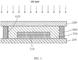
- FIG. 1 is a schematic diagram of a conventional encapsulation process of OLED, as shown in FIG. 1 , an existing encapsulation structure of OLED includes a TFT substrate 100 and an encapsulation cover plate 200 disposed opposite to each other, an OLED device 300 disposed between the TFT substrate 100 and the encapsulation cover plate 200 and disposed on the TFT substrate 100, a sealant 600 disposed between the TFT substrate 100 and the encapsulation cover plate 200 and forming a sealed space 610 between the TFT substrate 100 and the encapsulation cover plate 200, an encapsulation material 700 filled in the sealed space 610.
- the encapsulation material 700 is UV light cured from a side of the encapsulation cover plate 200, when the encapsulation material 700 is solidified by the UV light, at the same time, the performance of the TFT device in the TFT substrate 100 is affected, and cause the TFT device in the TFT substrate 100 to electrically shifted, and reduce the overall image display quality.
- An object of the present application is to provide an encapsulation method for an OLED capable of reducing or eliminating the influence of UV light to the TFT during UV light curing of the encapsulation material and the sealant.
- the object of the present application is also to provide encapsulation structure of an OLED, obtained by the above method, and the TFT thereof has excellent electrical performance.
- the present application provides an encapsulation method for an OLED, including the following steps:
- An UV light transmittance of the UV light absorption layer is less than 5%, and a transmittance of the visible light is more than 80%, the UV light absorbing layer has a thickness of 1 ⁇ m to 10 ⁇ m, a content of the inorganic particles in the UV light absorbing layer is 0.1 vol% to 1.0 vol%, and the inorganic particles have a particle size of 1 nm to 150 nm.
- the organic resin includes one or more of polyurethane, acrylic resin and epoxy resin
- the inorganic particles includes one or more of metal oxide particles and metal oxide modified particles
- the metal oxide particles includes one or more of titanium oxide particles, zinc oxide particles, and cerium oxide particles
- the metal oxide modified particles includes one or more of titanium oxide modified particles, zinc oxide modified particles, and cerium oxide modified particles.
- the method for forming the UV light absorbing layer includes dispersing the inorganic particles in a solution of an organic resin precursor to prepare a UV light absorbing solution, forming a film of the UV light absorbing layer on the outer surface of the first passivation layer by the UV light absorbing solution by adapting a solution film casting process, curing to form the UV light absorbing layer, the solution film casting process includes one or more of spin coating, one drop filling, ink jet printing, tape casting, and nozzle printing.
- the step S2 further includes: forming a second passivation layer covering the UV light absorption layer on the outer surface of the UV light absorption layer.
- the present application further includes an encapsulation structure of an OLED, including: a TFT substrate and a encapsulation cover disposed opposite to each other, an OLED device disposed between the TFT substrate and the encapsulation cover, and the OLED device disposed on the TFT substrate, a first passivation layer disposed on an outer surface of the OLED device and covering the OLED device, an UV light absorption layer disposed on an outer surface of the first passivation layer and covering the first passivation layer, a sealant disposed between the TFT substrate and the encapsulation cover and enclosing a sealed space between the TFT substrate and the encapsulation cover, and an encapsulation material filled in the sealed space 61.
- the sealant is disposed on a periphery of the OLED device, the UV light absorbing layer includes an organic resin and inorganic particles having UV light absorbing property dispersed in the organic resin, and the UV light absorbing layer is transparent.
- An UV light transmittance of the UV light absorption layer is less than 5%, and a transmittance of the visible light is more than 80%, the UV light absorbing layer has a thickness of 1 ⁇ m to 10 ⁇ m, a content of the inorganic particles in the UV light absorbing layer is 0.1vol% to 1.0vol%, and the inorganic particles have a particle size of 1 nm to 150 nm.
- the organic resin includes one or more of polyurethane, acrylic resin and epoxy resin
- the inorganic particles includes one or more of metal oxide particles and metal oxide modified particles
- the metal oxide particles includes one or more of titanium oxide particles, zinc oxide particles, and cerium oxide particles
- the metal oxide modified particles includes one or more of titanium oxide modified particles, zinc oxide modified particles, and cerium oxide modified particles.
- the OLED further includes a second passivation layer formed and covered the UV light absorption layer on the outer surface of the UV light absorption layer.
- Both materials of the first passivation layer and the second passivation layer includes silicon nitride, both thickness of the first passivation layer and the second passivation layer is 500 nm-800 nm, and a material of the encapsulation material includes one or more of polyurethane, acrylic resin and epoxy resin.
- the present application further includes an encapsulation method for an OLED, including the following steps:
- An UV light transmittance of the UV light absorption layer is less than 5%, and a transmittance of the visible light is more than 80%, the UV light absorbing layer has a thickness of 1 ⁇ m to 10 ⁇ m, a content of the inorganic particles in the UV light absorbing layer is 0. 1vol% to 1.0vol%, and the inorganic particles have a particle size of 1 nm to 150 nm.
- the organic resin includes one or more of polyurethane, acrylic resin and epoxy resin
- the inorganic particles includes one or more of metal oxide particles and metal oxide modified particles
- the metal oxide particles includes one or more of titanium oxide particles, zinc oxide particles, and cerium oxide particles
- the metal oxide modified particles includes one or more of titanium oxide modified particles, zinc oxide modified particles, and cerium oxide modified particles.
- the method for forming the UV light absorbing layer includes dispersing the inorganic particles in a solution of an organic resin precursor to prepare a UV light absorbing solution, forming a film of the UV light absorbing layer on the outer surface of the first passivation layer by the UV light absorbing solution by adapting a solution film casting process, curing to form the UV light absorbing layer, the solution film casting process includes one or more of spin coating, one drop filling, ink jet printing, tape casting, and nozzle printing.
- the step S2 further includes: forming a second passivation layer covering the UV light absorption layer on the outer surface of the UV light absorption layer.
- the beneficial effects of the present application are as follows: in the encapsulation method for an OLED of the present application, by disposing the UV light absorbing layer on the surface of the OLED device, in one aspect, the UV light absorbing layer has a low UV transmittance. Therefore, UV light can be blocked from being directed to the TFT during UV curing of the encapsulation material and the sealant to reduce or eliminate the influence of UV light on the TFT; on the other hand, the UV light absorbing layer has high visible light transmittance and therefore does not reduce the light intensity of the OLED device.
- the encapsulation structure of the OLED of the present application is fabricated by the above encapsulation method.
- the TFT has excellent electrical performance and the OLED device thereof has strong light intensity.
- the present application provides an encapsulation method for the OLED including the following steps: Step S1, as shown in FIG. 3 , providing a TFT substrate 10, fabricating an OLED device 30 on the TFT substrate 10; forming a first passivation layer 41 covering the OLED device 30 on an outer surface of the OLED device 30.
- the OLED device 30 includes an anode 31, a hole injection layer 32, a hole transport layer 33, a light-emitting layer 34, and an electron transport layer 35, an electron injection layer 36, and a cathode 37 sequentially arranged from bottom to top on the TFT substrate 10.
- the anode 31, the hole injection layer 32, the hole transport layer 33, the light-emitting layer 34, the electron transport layer 35, the electron injection layer 36 and the cathode 37 are all fabricated by the vapor deposition method.
- the material of the first passivation layer 41 includes silicon nitride
- the thickness of the first passivation layer 41 is 500 nm-800 nm
- the first passivation layer 41 is fabricated by a plasma enhanced chemical vapor deposition method, PECVD.
- the process conditions for fabricating the first passivation layer 41 by the plasma enhanced chemical vapor deposition method are as follows: the reaction gas is monosilane (SiH4) with a purity of more than 99.99% and ammonia (NH 3 ) with a purity of more than 99.99%, the auxiliary ionization gas is argon (Ar) with a purity of more than 99.99%, the power of the RF power is 10 W-500 W, the pressure of the deposition chamber is 10 Pa-20 Pa, and the deposition rate is 3 nm/s-20 nm/s.
- the reaction gas is monosilane (SiH4) with a purity of more than 99.99% and ammonia (NH 3 ) with a purity of more than 99.99%
- the auxiliary ionization gas is argon (Ar) with a purity of more than 99.99%
- the power of the RF power is 10 W-500 W
- the pressure of the deposition chamber is 10 Pa-20 Pa
- the deposition rate is 3 n
- an UV light absorbing layer 50 covering the first passivation layer 41 is fabricated on the outer surface of the first passivation layer 41.
- the UV light absorbing layer 50 includes an organic resin and inorganic particles having UV light absorbing property dispersed in the organic resin, and the UV light absorbing layer 50 is transparent.
- an UV light transmittance of the UV light absorption layer 50 is less than 5%, and a transmittance of the visible light is more than 80%.
- the UV light absorbing layer 50 has a thickness of 1 ⁇ m to 10 ⁇ m.
- the content of the inorganic particles in the UV light absorbing layer 50 is 0.1 vol% to 1.0 vol%.
- the major material of the UV light absorbing layer 50 is the organic resin
- the organic resin can be selected from one or more than one of organic resins having high visible light transmittance and good transparency, such as polyurethane, acrylic resin and epoxy resin.
- the acrylic resin is acrylic resin (that is polymethylmethacrylate).
- the inorganic particles can be selected from one or more than one of inorganic particles having low UV light transmittance and high visible light transmittance, such as metal oxide particles and metal oxide modified particles, and the metal oxide particles includes one or more of titanium oxide (TiO 2 ) particles, zinc oxide (ZnO) particles, and cerium oxide (CeO 2 ) particles, the metal oxide modified particles includes one or more of titanium oxide modified particles, zinc oxide modified particles, and cerium oxide modified particles.
- inorganic particles having low UV light transmittance and high visible light transmittance such as metal oxide particles and metal oxide modified particles
- the metal oxide particles includes one or more of titanium oxide (TiO 2 ) particles, zinc oxide (ZnO) particles, and cerium oxide (CeO 2 ) particles
- the metal oxide modified particles includes one or more of titanium oxide modified particles, zinc oxide modified particles, and cerium oxide modified particles.
- the metal oxide modified particles refer to particles of a metal oxide modified material obtained by doping with other chemical substances in the metal oxide material. By doping the other chemical elements, the UV light absorption performance of the metal oxide modified material is improved, greater than the UV light absorption performance of the original metal oxide material.
- the zinc oxide modified particles are aluminum-doped zinc oxide (Al-ZnO) particles.
- the inorganic particles have a particle size of 1 nm to 150 nm.
- the inorganic particles have a particle size of 20 nm to 50 nm.
- the method for fabricating the UV light absorbing layer 50 is by dispersing the inorganic particles in a solution of an organic resin precursor to prepare a UV light absorbing solution, the UV light absorbing solution is formed on the outer surface of the first passivation layer 41 by a solution film casting process to obtain the UV light absorbing layer 50 after being cured.
- the UV light absorbing solution is formed on the outer surface of the first passivation layer 41 by a solution film casting process to obtain the UV light absorbing layer 50 after being cured.
- the solution film casting process includes one or more of the following methods: spin coating, one drop filling, ODF, ink jet printing, IJP, tape casting, and nozzle printing.
- the inorganic particles are zinc oxide (ZnO) particles
- the zinc oxide particles have a particle size of 20 nm-50 nm
- the zinc oxide particles in the UV light absorption solution the content of the zinc oxide particles in the UV light absorbing solution is from 0.1% to 1.0% by volume
- the organic resin precursor solution is the methyl methacrylate monomer solution
- the UV light absorbing solution also contains an initiator that is uniformly dispersed therein
- the solution film casting process is ink jet printing, IJP
- the thickness of the uncured film formed on the outer surface of the first passivation layer 41 is 1.0 ⁇ m-5.0 ⁇ m.
- the step S2 may further include: forming a second passivation layer 42 covering the UV light absorption layer 50 on the outer surface of the UV light absorption layer 50.
- the material of the second passivation layer 42 includes silicon nitride, the second passivation layer 42 has a thickness of 500 nm-800 nm, and the second passivation layer 42 is fabricated by using the plasma enhanced chemical vapor deposition method, PECVD
- the process conditions for fabricating the second passivation layer 42 by the plasma enhanced chemical vapor deposition method are as follows: the reaction gas is monosilane (SiH 4 ) with a purity of more than 99.99% and ammonia (NH 3 ) with a purity of more than 99.99%
- the auxiliary ionization gas is argon (Ar) with a purity of more than 99.99%
- the power of the RF power is 10 W-500 W
- the pressure of the deposition chamber is 10 Pa-20 Pa
- the deposition rate is 3 nm/s-20 nm/s.
- step S3 as shown in FIG. 7 , providing an encapsulation cover 20, coating a sealant 60 on a periphery of the encapsulation cover 20 corresponding to the OLED device 30, and disposing an encapsulation material 70 in a region surrounded by the sealant 60 on the encapsulation cover 20.
- the encapsulation material 70 is an uncured liquid material (corresponding to a UV curing Dam & Fill encapsulation process) or a cured film (corresponding to a UV curing face sealant & film encapsulation process).
- step S3 when the encapsulation material 70 is an uncured liquid material, the encapsulation material 70 is coated or printed on the encapsulation plate 20. When the encapsulation material 70 is a cured film, the encapsulation material 70 is attached to the encapsulation cover 20.
- the encapsulation material 70 includes one or more of organic resins having high visible light transmittance and good transparency, such as polyurethane, acrylic resin and epoxy resin.
- organic resins having high visible light transmittance and good transparency such as polyurethane, acrylic resin and epoxy resin.
- the acrylic resin is acrylic resin (that is polymethylmethacrylate).
- the encapsulation material 70 is the same material as the organic resin in the UV light absorbing layer 50.
- the encapsulation material 70 can improve the mechanical performance of the Encapsulation structure of OLED prepared subsequently, and in addition, can eliminate the Newton ring and improve the display performance.
- step S4 aligning the encapsulation cover 20 and the TFT substrate 10, the sealant 60 is adhered to the TFT substrate 10 and the encapsulation cover 20 respectively, and forming the sealed space 61 between the TFT substrate 10 and the encapsulation cover 20, the encapsulation material 70 is filled in the sealed space 61.
- step S4 further includes a step of curing the sealant 60 by UV light.
- the step S4 further includes a step of simultaneously performing UV light curing on the encapsulation material 70 and the sealant 60.
- the UV light curing is simultaneously performed on the encapsulation material 70 and the sealant 60 by irradiating the encapsulation material 70 and the sealant 60 with UV light from the side of the encapsulating cover 20 for curing.
- the UV light has a wavelength of 365 nm and the UV light has an intensity of 5000 MJ/cm 2 to 9000 MJ/cm 2 .
- the UV light absorbing layer 50 is disposed on the surface of the OLED device 30, in one aspect, the UV light absorbing layer 50 has a low UV transmittance. Therefore, UV light can be blocked from being directed to the TFT during UV curing of the encapsulation material 70 and the sealant 60 to reduce or eliminate the influence of UV light on the TFT; on the other hand, the UV light absorbing layer 50 has high visible light transmittance and therefore does not reduce the light intensity of the OLED device 30.
- the present application provides an encapsulation structure of OLED including: a TFT substrate 10 and a encapsulation cover 20 disposed opposite to each other, an OLED device 30 disposed between the TFT substrate 10 and the encapsulation cover, and the OLED device 30 disposed on the TFT substrate 10, the first passivation layer 41 provided on the outer surface of the OLED device 30 and covering the OLED device 30, the UV light absorption layer 50 provided on the outer surface of the first passivation layer 41 and covering the first passivation layer 41, the sealant 60 provided between the TFT substrate 10 and the encapsulation cover 20 and enclosing the sealed space 61 between the TFT substrate 10 and the encapsulation cover 20, and the encapsulation material 70 filled in the sealed space 61.
- the sealant 60 is disposed on the periphery of the OLED device 30.
- the UV light absorbing layer 50 includes organic resin and inorganic particles dispersed in the organic resin and having UV light absorbing property.
- the UV light absorbing layer 50 is transparent.
- the OLED device 30 includes the anode 31, the hole injection layer 32, the hole transport layer 33, the light-emitting layer 34, and the electron transport layer 35, the electron injection layer 36, and the cathode 37 sequentially arranged from bottom to top on the TFT substrate 10.
- the material of the first passivation layer 41 includes silicon nitride, and the thickness of the first passivation layer 41 is 500 nm-800 nm.
- the UV light absorption layer 50 has an UV light transmittance of less than 5% and a visible light transmittance of more than 80%.
- the UV LIGHT absorbing layer 50 has a thickness of 1 ⁇ m to 10 ⁇ m.
- the content of the inorganic particles in the UV light absorbing layer 50 is 0.1 vol% to 1.0 vol%.
- the major material of the UV light absorbing layer 50 is the organic resin
- the organic resin can be selected from one or more than one of organic resins having high visible light transmittance and good transparency, such as polyurethane, acrylic resin and epoxy resin.
- the acrylic resin is acrylic resin (that is polymethylmethacrylate).
- the inorganic particles can be selected from one or more than one of inorganic particles having low UV light transmittance and high visible light transmittance, such as metal oxide particles and metal oxide modified particles, and the metal oxide particles includes one or more of titanium oxide (TiO 2 ) particles, zinc oxide (ZnO) particles, and cerium oxide (CeO 2 ) particles, the metal oxide modified particles includes one or more of titanium oxide modified particles, zinc oxide modified particles, and cerium oxide modified particles.
- inorganic particles having low UV light transmittance and high visible light transmittance such as metal oxide particles and metal oxide modified particles
- the metal oxide particles includes one or more of titanium oxide (TiO 2 ) particles, zinc oxide (ZnO) particles, and cerium oxide (CeO 2 ) particles
- the metal oxide modified particles includes one or more of titanium oxide modified particles, zinc oxide modified particles, and cerium oxide modified particles.
- the metal oxide modified particles refer to particles of a metal oxide modified material obtained by doping with other chemical substances in the metal oxide material. By doping the other chemical elements, the UV light absorption performance of the metal oxide modified material is improved, greater than the UV light absorption performance of the original metal oxide material.
- the zinc oxide modified particles are aluminum-doped zinc oxide (Al-ZnO) particles.
- the inorganic particles have a particle size of 1 nm to 150 nm.
- the inorganic particles have a particle size of 20 nm to 50 nm.
- the encapsulation structure of OLED may further include a second passivation layer 42 disposed on the outer surface of the UV light absorbing layer 50 and covering the UV light absorbing layer 50.
- the material of the second passivation layer 42 includes silicon nitride, and the thickness of the second passivation layer 42 is 500 nm-800 nm.
- the encapsulation material 70 includes one or more of organic resins having high visible light transmittance and good transparency, such as polyurethane, acrylic resin and epoxy resin.
- organic resins having high visible light transmittance and good transparency such as polyurethane, acrylic resin and epoxy resin.
- the acrylic resin is acrylic resin (that is polymethylmethacrylate).
- the encapsulation material 70 is the same material as the organic resin in the UV light absorbing layer 50.
- the UV light absorbing layer 50 is disposed on the surface of the OLED device 30, in one aspect, the UV light absorbing layer 50 has a low UV transmittance. Therefore, UV light can be blocked from being directed to the TFT during UV curing of the encapsulation material 70 and the sealant 60 to reduce or eliminate the influence of UV light on the TFT; on the other hand, the UV light absorbing layer 50 has high visible light transmittance and therefore does not reduce the light intensity of the OLED device 30.
- the present application provides an encapsulation method for OLED and an encapsulation structure of OLED.
- the UV light absorbing layer has a low UV transmittance. Therefore, UV light can be blocked from being directed to the TFT during UV curing of the encapsulation material and the sealant to reduce or eliminate the influence of UV light on the TFT; on the other hand, the UV light absorbing layer has high visible light transmittance and therefore does not reduce the light intensity of the OLED device.
- the encapsulation structure of the OLED of the present application is fabricated by the above encapsulation method.
- the TFT has excellent electrical performance and the OLED device thereof has strong light intensity.
Landscapes
- Engineering & Computer Science (AREA)
- Manufacturing & Machinery (AREA)
- Microelectronics & Electronic Packaging (AREA)
- Electroluminescent Light Sources (AREA)
Abstract
Description
- The disclosure relates to a display technical field, and more particularly to an encapsulation method for an OLED and an Encapsulation structure of OLED.
- Organic Light Emitting Diode (OLED) has been widely used in the field of display, lighting and smart wearable for its advantages of good self-luminous characteristics, high contrast, fast response and flexible display and etc.
- With the development of science technology, OLED technology has become an important candidate for the third generation of display technology used for consumer electronics such as mobile phones, computers, televisions, etc. The basic display principle of OLED is as follows: driven by an electric field, the organic material emits light by the injection and recombination of carriers. OLED can be independently illuminated by RGB pixels, white OLED combined with color filter or blue OLED with light color conversion to achieve full color display. OLED display technology can make the panel thinner; its self-luminous characteristics can also achieve higher contrast in the wild evening, and can be made on the substrate of different materials, and can be made as a flexible display device.
- Green environment and energy-efficient way of life has become the trend of people's lives, so OLED is considered as the future lighting technology. Light-emitting materials of OLED are organic semiconductors; the material properties of the light-emitting layer can be controlled to produce light with different wavelengths. OLED is a planar light source with soft light. Its illumination can achieve thinner, if the OLED is fabricated on a flexible substrate, it can realize a large area and a flexible light source, and has potential applications in home decoration and the like.
- Smart wear market will be an important direction for OLED technology development. The thin, flexible and portable properties of flexible AMOLEDs (active matrix organic light-emitting diodes) determine that there will be wider room for application on wearable devices. OLED display panel can be equipped to a bracelet or watch; it can achieve the perfect fit with the wrist, but also can realize making calls, internet and other functions.
- In addition, OLED has potential applications in car audio display, smart home, aerospace technology.
- The difference between OLED and conventional LCD is that a backlight is no more needed, through the carriers of both electron and hole to inject the organic thin-film organic materials and recombination to emit light in the organic materials. However, the organic materials are very sensitive to moisture and oxygen. The permeation of water/oxygen is greatly reducing the lifetime of the device. To meet the commercialized requirements for the lifetime and stability of OLED device, the OLED devices have very high requirements for encapsulation: the lifetime is at least 104 hours, the transmission rate of water vapor is less than 10-6 g/m2/day, and the transmission rate of oxygen is less than 10-5 g/m2/day (1atm). Therefore, encapsulation in the fabrication of OLED devices is in an important position, is one of the key factors affecting the yield of the product.
- The encapsulation methods for existing OLED device mainly include glass encapsulation, that is, the encapsulation glass is coated with a UV light curable sealant, a laser sealing for laser-encapsulation, or a sealant and filing a Dam & Fill desiccant and cured to provide a relatively confined environment for the light-emitting device, to achieve good water/oxygen barrier capability in a certain period of time.
- Flexible OLED panel is an important research direction of organic light-emitting devices. In recent two years, the exploration of encapsulation of flexible OLED devices is in full swing. Thin film encapsulation using plasma enhanced chemical vapor deposition, PECVD or atomic layer deposition, ALD has become a research hotspot. However, the encapsulation cost of flexible OLED devices is 1 to 5 times of the cost of conventional cover encapsulation devices. Although the flexible OLED display is the future trends, but the conventional flat glass OLED encapsulation device does not disappear.
- TFTs play an important role in active matrix driven display devices, AMOLEDs, typically as switching devices and driving devices in display devices. By the high UV light energy, TFTs generate carriers, electrons or holes under light irradiation, when the free carrier concentration increases, the threshold voltage, Vth decreases, and the Vth shifting directly causes the luminance of the pixel to be changed, thereby affecting the overall display quality. Therefore, the long-term stability of the TFT display device is very important.
- The encapsulation for large-size devices need to add filler to improve the mechanical properties of the device, in addition to eliminate Newton ring (especially for top-emitting devices, Newton rings must be eliminated). Currently filler has two major categories according to the method for curing: UV light curing and thermal curing. Wherein, UV light curing process is simple, curing time is short, usually 5min-15min, Tact time of mass production can be shortened; its shortcomings are UV light is irradiated to the device from a side of the cover plate, during trigger curing of the filler, it causes TFT electrical shift at the same time, reducing the overall image display quality. A temperature of thermal curing of the Filler currently in the market is about 100 , curing time up to 60min-90min; In addition, the temperature uniformity of the oven adapted has a significant impact on the degree of curing the filler, uneven curing of the filler will result encapsulation mura (phenomenon of uneven brightness of the display device).
-
FIG. 1 is a schematic diagram of a conventional encapsulation process of OLED, as shown inFIG. 1 , an existing encapsulation structure of OLED includes aTFT substrate 100 and anencapsulation cover plate 200 disposed opposite to each other, anOLED device 300 disposed between theTFT substrate 100 and theencapsulation cover plate 200 and disposed on theTFT substrate 100, asealant 600 disposed between theTFT substrate 100 and theencapsulation cover plate 200 and forming a sealedspace 610 between theTFT substrate 100 and theencapsulation cover plate 200, anencapsulation material 700 filled in the sealedspace 610. - As shown in
FIG. 1 , when theencapsulation material 700 is UV light cured from a side of theencapsulation cover plate 200, when theencapsulation material 700 is solidified by the UV light, at the same time, the performance of the TFT device in theTFT substrate 100 is affected, and cause the TFT device in theTFT substrate 100 to electrically shifted, and reduce the overall image display quality. - An object of the present application is to provide an encapsulation method for an OLED capable of reducing or eliminating the influence of UV light to the TFT during UV light curing of the encapsulation material and the sealant.
- The object of the present application is also to provide encapsulation structure of an OLED, obtained by the above method, and the TFT thereof has excellent electrical performance.
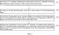
- In order to achieve the above object, the present application provides an encapsulation method for an OLED, including the following steps:
- Step S1: providing a TFT substrate, fabricating an OLED device on the TFT substrate; forming a first passivation layer covering an outer surface of the OLED device.
- Step S2: forming an UV light absorbing layer covering an outer surface of the first passivation layer, the UV light absorbing layer including an organic resin and inorganic particles having UV light absorbing property dispersed in the organic resin, and the UV light absorbing layer is transparent.
- Step S3: providing an encapsulation cover, coating a sealant on a periphery of the encapsulation cover corresponding to the OLED device, and disposing an encapsulation material in a region surrounded by the sealant on the encapsulation cover.
- Step S4: aligning the encapsulation cover and the TFT substrate, the sealant being adhered to the TFT substrate and the encapsulation cover respectively, and forming a sealed space between the TFT substrate and the encapsulation cover, the encapsulation material filled in the sealed space.
- An UV light transmittance of the UV light absorption layer is less than 5%, and a transmittance of the visible light is more than 80%, the UV light absorbing layer has a thickness of 1 µm to 10 µm, a content of the inorganic particles in the UV light absorbing layer is 0.1 vol% to 1.0 vol%, and the inorganic particles have a particle size of 1 nm to 150 nm.
- The organic resin includes one or more of polyurethane, acrylic resin and epoxy resin, the inorganic particles includes one or more of metal oxide particles and metal oxide modified particles, the metal oxide particles includes one or more of titanium oxide particles, zinc oxide particles, and cerium oxide particles, and the metal oxide modified particles includes one or more of titanium oxide modified particles, zinc oxide modified particles, and cerium oxide modified particles.
- The method for forming the UV light absorbing layer includes dispersing the inorganic particles in a solution of an organic resin precursor to prepare a UV light absorbing solution, forming a film of the UV light absorbing layer on the outer surface of the first passivation layer by the UV light absorbing solution by adapting a solution film casting process, curing to form the UV light absorbing layer, the solution film casting process includes one or more of spin coating, one drop filling, ink jet printing, tape casting, and nozzle printing.
- The step S2 further includes: forming a second passivation layer covering the UV light absorption layer on the outer surface of the UV light absorption layer.
- The present application further includes an encapsulation structure of an OLED, including:
a TFT substrate and a encapsulation cover disposed opposite to each other, an OLED device disposed between the TFT substrate and the encapsulation cover, and the OLED device disposed on the TFT substrate, a first passivation layer disposed on an outer surface of the OLED device and covering the OLED device, an UV light absorption layer disposed on an outer surface of the first passivation layer and covering the first passivation layer, a sealant disposed between the TFT substrate and the encapsulation cover and enclosing a sealed space between the TFT substrate and the encapsulation cover, and an encapsulation material filled in the sealedspace 61. - The sealant is disposed on a periphery of the OLED device, the UV light absorbing layer includes an organic resin and inorganic particles having UV light absorbing property dispersed in the organic resin, and the UV light absorbing layer is transparent.
- An UV light transmittance of the UV light absorption layer is less than 5%, and a transmittance of the visible light is more than 80%, the UV light absorbing layer has a thickness of 1µm to 10µm, a content of the inorganic particles in the UV light absorbing layer is 0.1vol% to 1.0vol%, and the inorganic particles have a particle size of 1 nm to 150 nm.
- The organic resin includes one or more of polyurethane, acrylic resin and epoxy resin, the inorganic particles includes one or more of metal oxide particles and metal oxide modified particles, the metal oxide particles includes one or more of titanium oxide particles, zinc oxide particles, and cerium oxide particles, and the metal oxide modified particles includes one or more of titanium oxide modified particles, zinc oxide modified particles, and cerium oxide modified particles.
- The OLED further includes a second passivation layer formed and covered the UV light absorption layer on the outer surface of the UV light absorption layer.
- Both materials of the first passivation layer and the second passivation layer includes silicon nitride, both thickness of the first passivation layer and the second passivation layer is 500 nm-800 nm, and a material of the encapsulation material includes one or more of polyurethane, acrylic resin and epoxy resin.
- The present application further includes an encapsulation method for an OLED, including the following steps:
- Step S1: providing a TFT substrate, fabricating an OLED device on the TFT substrate; forming a first passivation layer covering an outer surface of the OLED device.
- Step S2: forming an UV light absorbing layer covering an outer surface of the first passivation layer, the UV light absorbing layer including an organic resin and inorganic particles having UV light absorbing property dispersed in the organic resin, and the UV light absorbing layer is transparent.
- Step S3: providing an encapsulation cover, coating a sealant on a periphery of the encapsulation cover corresponding to the OLED device, and disposing an encapsulation material in a region surrounded by the sealant on the encapsulation cover.
- Step S4: aligning the encapsulation cover and the TFT substrate, the sealant being adhered to the TFT substrate and the encapsulation cover respectively, and forming a sealed space between the TFT substrate and the encapsulation cover, the encapsulation material filled in the sealed space.
- An UV light transmittance of the UV light absorption layer is less than 5%, and a transmittance of the visible light is more than 80%, the UV light absorbing layer has a thickness of 1 µm to 10µm, a content of the inorganic particles in the UV light absorbing layer is 0. 1vol% to 1.0vol%, and the inorganic particles have a particle size of 1 nm to 150 nm.
- The organic resin includes one or more of polyurethane, acrylic resin and epoxy resin, the inorganic particles includes one or more of metal oxide particles and metal oxide modified particles, the metal oxide particles includes one or more of titanium oxide particles, zinc oxide particles, and cerium oxide particles, and the metal oxide modified particles includes one or more of titanium oxide modified particles, zinc oxide modified particles, and cerium oxide modified particles.
- The method for forming the UV light absorbing layer includes dispersing the inorganic particles in a solution of an organic resin precursor to prepare a UV light absorbing solution, forming a film of the UV light absorbing layer on the outer surface of the first passivation layer by the UV light absorbing solution by adapting a solution film casting process, curing to form the UV light absorbing layer, the solution film casting process includes one or more of spin coating, one drop filling, ink jet printing, tape casting, and nozzle printing.
- The step S2 further includes: forming a second passivation layer covering the UV light absorption layer on the outer surface of the UV light absorption layer.
- The beneficial effects of the present application are as follows: in the encapsulation method for an OLED of the present application, by disposing the UV light absorbing layer on the surface of the OLED device, in one aspect, the UV light absorbing layer has a low UV transmittance. Therefore, UV light can be blocked from being directed to the TFT during UV curing of the encapsulation material and the sealant to reduce or eliminate the influence of UV light on the TFT; on the other hand, the UV light absorbing layer has high visible light transmittance and therefore does not reduce the light intensity of the OLED device. The encapsulation structure of the OLED of the present application is fabricated by the above encapsulation method. The TFT has excellent electrical performance and the OLED device thereof has strong light intensity.
- For further understanding of the features and technical contents of the present application, reference should be made to the following detailed description and accompanying drawings of the present application. However, the drawings are for reference only and are not intended to limit the present application.
- The technical solutions of the present application and other beneficial effects will be apparent from the following detailed description of specific embodiments of the present application with reference to the accompanying drawings.
-
FIG. 1 is a schematic diagram of a conventional encapsulation process of OLED. -
FIG. 2 is a flow chart of the encapsulation method for the OLED of the present application. -
FIG. 3 is a schematic view of step S1 of the encapsulation method for the OLED of the present application. -
FIG. 4 is a schematic diagram of the specific structure of the OLED device inFIG. 3 . -
FIG. 5 is a schematic diagram of a first embodiment of step S2 of the encapsulation method for the OLED of the present application. -
FIG. 6 is a schematic diagram of a second embodiment of the step S2 of the encapsulation method for the OLED of the present application. -
FIG. 7 is a schematic view of step S3 of the encapsulation method for the OLED of the present application. -
FIG. 8 is a schematic view of a first embodiment of step S4 of the encapsulation method for the OLED of the present application. -
FIG. 9 is a schematic view of a second embodiment of step S4 of the encapsulation method for the OLED of the present application. -
FIG. 10 is a schematic cross-sectional view of a first embodiment of the encapsulation structure of the OLED of the present application. -
FIG. 11 is a schematic cross-sectional view of a first embodiment of the encapsulation structure of the OLED of the present application. - To further illustrate the technical means adopted by the present application and the effects thereof, the following describes the preferred embodiments of the present application and the accompanying drawings in detail.
- Referring to
FIG. 2 , the present application provides an encapsulation method for the OLED including the following steps:
Step S1, as shown inFIG. 3 , providing aTFT substrate 10, fabricating anOLED device 30 on theTFT substrate 10; forming afirst passivation layer 41 covering theOLED device 30 on an outer surface of theOLED device 30. - Specifically, as shown in
FIG. 4 , theOLED device 30 includes ananode 31, ahole injection layer 32, ahole transport layer 33, a light-emittinglayer 34, and anelectron transport layer 35, anelectron injection layer 36, and acathode 37 sequentially arranged from bottom to top on theTFT substrate 10. - Specifically, the
anode 31, thehole injection layer 32, thehole transport layer 33, the light-emittinglayer 34, theelectron transport layer 35, theelectron injection layer 36 and thecathode 37 are all fabricated by the vapor deposition method. - Specifically, the material of the
first passivation layer 41 includes silicon nitride, the thickness of thefirst passivation layer 41 is 500 nm-800 nm, and thefirst passivation layer 41 is fabricated by a plasma enhanced chemical vapor deposition method, PECVD. - Preferably, the process conditions for fabricating the
first passivation layer 41 by the plasma enhanced chemical vapor deposition method are as follows: the reaction gas is monosilane (SiH4) with a purity of more than 99.99% and ammonia (NH3) with a purity of more than 99.99%, the auxiliary ionization gas is argon (Ar) with a purity of more than 99.99%, the power of the RF power is 10 W-500 W, the pressure of the deposition chamber is 10 Pa-20 Pa, and the deposition rate is 3 nm/s-20 nm/s. - In step S2, as shown in
FIG. 5 , an UVlight absorbing layer 50 covering thefirst passivation layer 41 is fabricated on the outer surface of thefirst passivation layer 41. The UVlight absorbing layer 50 includes an organic resin and inorganic particles having UV light absorbing property dispersed in the organic resin, and the UVlight absorbing layer 50 is transparent. - Specifically, an UV light transmittance of the UV
light absorption layer 50 is less than 5%, and a transmittance of the visible light is more than 80%. - Specifically, the UV
light absorbing layer 50 has a thickness of 1 µm to 10µm. - Specifically, the content of the inorganic particles in the UV
light absorbing layer 50 is 0.1 vol% to 1.0 vol%. - Specifically, the major material of the UV
light absorbing layer 50 is the organic resin, the organic resin can be selected from one or more than one of organic resins having high visible light transmittance and good transparency, such as polyurethane, acrylic resin and epoxy resin. Preferably, the acrylic resin is acrylic resin (that is polymethylmethacrylate). - Specifically, the inorganic particles can be selected from one or more than one of inorganic particles having low UV light transmittance and high visible light transmittance, such as metal oxide particles and metal oxide modified particles, and the metal oxide particles includes one or more of titanium oxide (TiO2) particles, zinc oxide (ZnO) particles, and cerium oxide (CeO2) particles, the metal oxide modified particles includes one or more of titanium oxide modified particles, zinc oxide modified particles, and cerium oxide modified particles.
- Specifically, the metal oxide modified particles refer to particles of a metal oxide modified material obtained by doping with other chemical substances in the metal oxide material. By doping the other chemical elements, the UV light absorption performance of the metal oxide modified material is improved, greater than the UV light absorption performance of the original metal oxide material.
- Preferably, the zinc oxide modified particles are aluminum-doped zinc oxide (Al-ZnO) particles.
- Specifically, the inorganic particles have a particle size of 1 nm to 150 nm. Preferably, the inorganic particles have a particle size of 20 nm to 50 nm.
- Specifically, the method for fabricating the UV
light absorbing layer 50 is by dispersing the inorganic particles in a solution of an organic resin precursor to prepare a UV light absorbing solution, the UV light absorbing solution is formed on the outer surface of thefirst passivation layer 41 by a solution film casting process to obtain the UVlight absorbing layer 50 after being cured. The UV light absorbing solution is formed on the outer surface of thefirst passivation layer 41 by a solution film casting process to obtain the UVlight absorbing layer 50 after being cured. - Specifically, the solution film casting process includes one or more of the following methods: spin coating, one drop filling, ODF, ink jet printing, IJP, tape casting, and nozzle printing.
- Preferably, in the method for fabricating the UV
light absorbing layer 50, the inorganic particles are zinc oxide (ZnO) particles, the zinc oxide particles have a particle size of 20 nm-50 nm, the zinc oxide particles in the UV light absorption solution, the content of the zinc oxide particles in the UV light absorbing solution is from 0.1% to 1.0% by volume, the organic resin precursor solution is the methyl methacrylate monomer solution, and the UV light absorbing solution also contains an initiator that is uniformly dispersed therein, the solution film casting process is ink jet printing, IJP, and the thickness of the uncured film formed on the outer surface of thefirst passivation layer 41 is 1.0 µm-5.0 µm. - Specifically, as shown in
FIG. 6 , the step S2 may further include: forming asecond passivation layer 42 covering the UVlight absorption layer 50 on the outer surface of the UVlight absorption layer 50. - Specifically, the material of the
second passivation layer 42 includes silicon nitride, thesecond passivation layer 42 has a thickness of 500 nm-800 nm, and thesecond passivation layer 42 is fabricated by using the plasma enhanced chemical vapor deposition method, PECVD - Preferably, the process conditions for fabricating the
second passivation layer 42 by the plasma enhanced chemical vapor deposition method are as follows: the reaction gas is monosilane (SiH4) with a purity of more than 99.99% and ammonia (NH3) with a purity of more than 99.99% The auxiliary ionization gas is argon (Ar) with a purity of more than 99.99%, the power of the RF power is 10 W-500 W, the pressure of the deposition chamber is 10 Pa-20 Pa, and the deposition rate is 3 nm/s-20 nm/s. - In step S3, as shown in
FIG. 7 , providing anencapsulation cover 20, coating asealant 60 on a periphery of theencapsulation cover 20 corresponding to theOLED device 30, and disposing anencapsulation material 70 in a region surrounded by thesealant 60 on theencapsulation cover 20. - Specifically, the
encapsulation material 70 is an uncured liquid material (corresponding to a UV curing Dam & Fill encapsulation process) or a cured film (corresponding to a UV curing face sealant & film encapsulation process). - In step S3, when the
encapsulation material 70 is an uncured liquid material, theencapsulation material 70 is coated or printed on theencapsulation plate 20. When theencapsulation material 70 is a cured film, theencapsulation material 70 is attached to theencapsulation cover 20. - Specifically, the
encapsulation material 70 includes one or more of organic resins having high visible light transmittance and good transparency, such as polyurethane, acrylic resin and epoxy resin. Preferably, the acrylic resin is acrylic resin (that is polymethylmethacrylate). - Preferably, the
encapsulation material 70 is the same material as the organic resin in the UVlight absorbing layer 50. - Specifically, the
encapsulation material 70 can improve the mechanical performance of the Encapsulation structure of OLED prepared subsequently, and in addition, can eliminate the Newton ring and improve the display performance. - In step S4, as shown in
FIG. 8 andFIG. 9 , aligning theencapsulation cover 20 and theTFT substrate 10, thesealant 60 is adhered to theTFT substrate 10 and theencapsulation cover 20 respectively, and forming the sealedspace 61 between theTFT substrate 10 and theencapsulation cover 20, theencapsulation material 70 is filled in the sealedspace 61. - Specifically, when the
encapsulation material 70 in step S3 is the cured film, the step S4 further includes a step of curing thesealant 60 by UV light. - Specifically, as shown in
FIG. 8 andFIG. 9 , when theencapsulation material 70 in the step S3 is an uncured liquid material, the step S4 further includes a step of simultaneously performing UV light curing on theencapsulation material 70 and thesealant 60. Preferably, the UV light curing is simultaneously performed on theencapsulation material 70 and thesealant 60 by irradiating theencapsulation material 70 and thesealant 60 with UV light from the side of the encapsulatingcover 20 for curing. The UV light has a wavelength of 365 nm and the UV light has an intensity of 5000 MJ/cm2 to 9000 MJ/cm2. - In the encapsulation method for the OLED of the present application, the UV
light absorbing layer 50 is disposed on the surface of theOLED device 30, in one aspect, the UVlight absorbing layer 50 has a low UV transmittance. Therefore, UV light can be blocked from being directed to the TFT during UV curing of theencapsulation material 70 and thesealant 60 to reduce or eliminate the influence of UV light on the TFT; on the other hand, the UVlight absorbing layer 50 has high visible light transmittance and therefore does not reduce the light intensity of theOLED device 30. - Referring to
FIG. 10 andFIG. 11 , and also referring toFIG. 4 , based on the above encapsulation method for the OLED, the present application provides an encapsulation structure of OLED including: aTFT substrate 10 and aencapsulation cover 20 disposed opposite to each other, anOLED device 30 disposed between theTFT substrate 10 and the encapsulation cover, and theOLED device 30 disposed on theTFT substrate 10, thefirst passivation layer 41 provided on the outer surface of theOLED device 30 and covering theOLED device 30, the UVlight absorption layer 50 provided on the outer surface of thefirst passivation layer 41 and covering thefirst passivation layer 41, thesealant 60 provided between theTFT substrate 10 and theencapsulation cover 20 and enclosing the sealedspace 61 between theTFT substrate 10 and theencapsulation cover 20, and theencapsulation material 70 filled in the sealedspace 61. - The
sealant 60 is disposed on the periphery of theOLED device 30. The UVlight absorbing layer 50 includes organic resin and inorganic particles dispersed in the organic resin and having UV light absorbing property. The UVlight absorbing layer 50 is transparent. - Specifically, as shown in
FIG. 4 , theOLED device 30 includes theanode 31, thehole injection layer 32, thehole transport layer 33, the light-emittinglayer 34, and theelectron transport layer 35, theelectron injection layer 36, and thecathode 37 sequentially arranged from bottom to top on theTFT substrate 10. - Specifically, the material of the
first passivation layer 41 includes silicon nitride, and the thickness of thefirst passivation layer 41 is 500 nm-800 nm. - Specifically, the UV
light absorption layer 50 has an UV light transmittance of less than 5% and a visible light transmittance of more than 80%. - Specifically, the UV
LIGHT absorbing layer 50 has a thickness of 1 µm to 10 µm. - Specifically, the content of the inorganic particles in the UV
light absorbing layer 50 is 0.1 vol% to 1.0 vol%. - Specifically, the major material of the UV
light absorbing layer 50 is the organic resin, the organic resin can be selected from one or more than one of organic resins having high visible light transmittance and good transparency, such as polyurethane, acrylic resin and epoxy resin. Preferably, the acrylic resin is acrylic resin (that is polymethylmethacrylate). - Specifically, the inorganic particles can be selected from one or more than one of inorganic particles having low UV light transmittance and high visible light transmittance, such as metal oxide particles and metal oxide modified particles, and the metal oxide particles includes one or more of titanium oxide (TiO2) particles, zinc oxide (ZnO) particles, and cerium oxide (CeO2) particles, the metal oxide modified particles includes one or more of titanium oxide modified particles, zinc oxide modified particles, and cerium oxide modified particles.
- Specifically, the metal oxide modified particles refer to particles of a metal oxide modified material obtained by doping with other chemical substances in the metal oxide material. By doping the other chemical elements, the UV light absorption performance of the metal oxide modified material is improved, greater than the UV light absorption performance of the original metal oxide material.
- Preferably, the zinc oxide modified particles are aluminum-doped zinc oxide (Al-ZnO) particles.
- Specifically, the inorganic particles have a particle size of 1 nm to 150 nm. Preferably, the inorganic particles have a particle size of 20 nm to 50 nm.
- Specifically, as shown in
FIG. 11 , the encapsulation structure of OLED may further include asecond passivation layer 42 disposed on the outer surface of the UVlight absorbing layer 50 and covering the UVlight absorbing layer 50. - Specifically, the material of the
second passivation layer 42 includes silicon nitride, and the thickness of thesecond passivation layer 42 is 500 nm-800 nm. - Specifically, the
encapsulation material 70 includes one or more of organic resins having high visible light transmittance and good transparency, such as polyurethane, acrylic resin and epoxy resin. Preferably, the acrylic resin is acrylic resin (that is polymethylmethacrylate). - Preferably, the
encapsulation material 70 is the same material as the organic resin in the UVlight absorbing layer 50. - In the encapsulation structure of the OLED of the present application, the UV
light absorbing layer 50 is disposed on the surface of theOLED device 30, in one aspect, the UVlight absorbing layer 50 has a low UV transmittance. Therefore, UV light can be blocked from being directed to the TFT during UV curing of theencapsulation material 70 and thesealant 60 to reduce or eliminate the influence of UV light on the TFT; on the other hand, the UVlight absorbing layer 50 has high visible light transmittance and therefore does not reduce the light intensity of theOLED device 30. - To sum up, the present application provides an encapsulation method for OLED and an encapsulation structure of OLED. In the encapsulation method for OLED of the present application, by disposing the UV light absorbing layer on the surface of the OLED device, in one aspect, the UV light absorbing layer has a low UV transmittance. Therefore, UV light can be blocked from being directed to the TFT during UV curing of the encapsulation material and the sealant to reduce or eliminate the influence of UV light on the TFT; on the other hand, the UV light absorbing layer has high visible light transmittance and therefore does not reduce the light intensity of the OLED device. The encapsulation structure of the OLED of the present application is fabricated by the above encapsulation method. The TFT has excellent electrical performance and the OLED device thereof has strong light intensity.
- The foregoing contents are detailed description of the disclosure in conjunction with specific preferred embodiments and concrete embodiments of the disclosure are not limited to these descriptions. For the person skilled in the art of the disclosure, without departing from the concept of the disclosure, simple deductions or substitutions can be made and should be included in the protection scope of the application.
Claims (11)
- An encapsulation method for an OLED, comprising the following steps:step S1: providing a TFT substrate, fabricating an OLED device on the TFT substrate; forming a first passivation layer covering an outer surface of the OLED device;step S2: forming an UV light absorbing layer covering an outer surface of the first passivation layer, the UV light absorbing layer comprising an organic resin and inorganic particles having UV light absorbing property dispersed in the organic resin, and the UV light absorbing layer is transparent;step S3: providing an encapsulation cover, coating a sealant on a periphery of the encapsulation cover corresponding to the OLED device, and disposing an encapsulation material in a region surrounded by the sealant on the encapsulation cover; andstep S4: aligning the encapsulation cover and the TFT substrate, the sealant being adhered to the TFT substrate and the encapsulation cover respectively, and forming a sealed space between the TFT substrate and the encapsulation cover, the encapsulation material filled in the sealed space.
- The encapsulation method for the OLED according to claim 1, wherein an UV light transmittance of the UV light absorption layer is less than 5%, and a transmittance of the visible light is more than 80%, the UV light absorbing layer has a thickness of 1 µm to 10 µm, a content of the inorganic particles in the UV light absorbing layer is 0.1 vol% to 1.0 vol%, the inorganic particles have a particle size of 1 nm to 150 nm.
- The encapsulation method for the OLED according to claim 1, wherein the organic resin comprises one or more of polyurethane, acrylic resin and epoxy resin, the inorganic particles comprise one or more of metal oxide particles and metal oxide modified particles, the metal oxide particles comprise one or more of titanium oxide particles, zinc oxide particles, and cerium oxide particles, and the metal oxide modified particles comprises one or more of titanium oxide modified particles, zinc oxide modified particles, and cerium oxide modified particles.
- The encapsulation method for the OLED according to claim 1, wherein the method for forming the UV light absorbing layer comprises dispersing the inorganic particles in a solution of an organic resin precursor to prepare a UV light absorbing solution, forming a film of the UV light absorbing layer on the outer surface of the first passivation layer by the UV light absorbing solution by adapting a solution film casting process, curing to form the UV light absorbing layer, the solution film casting process comprises one or more of spin coating, one drop filling, ink jet printing, tape casting, and nozzle printing.
- The encapsulation method for the OLED according to claim 1, wherein the step S2 further comprises: forming a second passivation layer covering the UV light absorption layer on the outer surface of the UV light absorption layer.
- An encapsulation structure of an OLED, comprising:a TFT substrate and a encapsulation cover disposed opposite to each other, an OLED device disposed between the TFT substrate and the encapsulation cover, and the OLED device disposed on the TFT substrate, a first passivation layer disposed on an outer surface of the OLED device and covering the OLED device, an UV light absorption layer disposed on an outer surface of the first passivation layer and covering the first passivation layer, a sealant disposed between the TFT substrate and the encapsulation cover and enclosing a sealed space between the TFT substrate and the encapsulation cover, and an encapsulation material filled in the sealed space; andwherein the sealant is disposed on a periphery of the OLED device, the UV light absorbing layer comprises an organic resin and inorganic particles having UV light absorbing property dispersed in the organic resin, and the UV light absorbing layer is transparent.
- The encapsulation structure of the OLED according to claim 6, wherein an UV light transmittance of the UV light absorption layer is less than 5%, and a transmittance of the visible light is more than 80%, the UV light absorbing layer has a thickness of 1 µm to 10 µm, a content of the inorganic particles in the UV light absorbing layer is 0.1 vol% to 1.0 vol%, the inorganic particles have a particle size of 1 nm to 150 nm.
- The encapsulation structure of the OLED according to claim 6, wherein the organic resin comprises one or more of polyurethane, acrylic resin and epoxy resin, the inorganic particles comprise one or more of metal oxide particles and metal oxide modified particles, the metal oxide particles comprise one or more of titanium oxide particles, zinc oxide particles, and cerium oxide particles, and the metal oxide modified particles comprises one or more of titanium oxide modified particles, zinc oxide modified particles, and cerium oxide modified particles.
- The encapsulation structure of the OLED according to claim 6, further comprises a second passivation layer formed and covered the UV light absorption layer on the outer surface of the UV light absorption layer.
- The encapsulation structure of the OLED according to claim 9, wherein both materials of the first passivation layer and the second passivation layer comprise silicon nitride, both thickness of the first passivation layer and the second passivation layer is 500 nm-800 nm, and a material of the encapsulation material comprises one or more of polyurethane, acrylic resin and epoxy resin.
- An encapsulation method for an OLED, comprising the following steps:step S1: providing a TFT substrate, fabricating an OLED device on the TFT substrate; forming a first passivation layer covering an outer surface of the OLED device;step S2: forming an UV light absorbing layer covering an outer surface of the first passivation layer, the UV light absorbing layer comprising an organic resin and inorganic particles having UV light absorbing property dispersed in the organic resin, and the UV light absorbing layer is transparent;step S3: providing an encapsulation cover, coating a sealant on a periphery of the encapsulation cover corresponding to the OLED device, and disposing an encapsulation material in a region surrounded by the sealant on the encapsulation cover;step S4: aligning the encapsulation cover and the TFT substrate, the sealant being adhered to the TFT substrate and the encapsulation cover respectively, and forming a sealed space between the TFT substrate and the encapsulation cover, the encapsulation material filled in the sealed space;wherein an UV light transmittance of the UV light absorption layer is less than 5%, and a transmittance of the visible light is more than 80%, the UV light absorbing layer has a thickness of 1 µm to 10 µm, a content of the inorganic particles in the UV light absorbing layer is 0.1vol% to 1.0vol%, and the inorganic particles have a particle size of 1 nm to 150 nm;wherein the organic resin comprises one or more of polyurethane, acrylic resin and epoxy resin, the inorganic particles comprises one or more of metal oxide particles and metal oxide modified particles, the metal oxide particles comprises one or more of titanium oxide particles, zinc oxide particles, and cerium oxide particles, and the metal oxide modified particles comprises one or more of titanium oxide modified particles, zinc oxide modified particles, and cerium oxide modified particles;wherein the method for forming the UV light absorbing layer comprises dispersing the inorganic particles in a solution of an organic resin precursor to prepare a UV light absorbing solution, forming a film of the UV light absorbing layer on the outer surface of the first passivation layer by the UV light absorbing solution by adapting a solution film casting process, curing to form the UV light absorbing layer, the solution film casting process comprises one or more of spin coating, one drop filling, ink jet printing, tape casting, and nozzle printing; andwherein the step S2 further comprises: forming a second passivation layer covering the UV light absorption layer on the outer surface of the UV light absorption layer.
Applications Claiming Priority (2)
| Application Number | Priority Date | Filing Date | Title |
|---|---|---|---|
| CN201711060227.5A CN107946480A (en) | 2017-11-01 | 2017-11-01 | OLED encapsulation method and OLED encapsulating structures |
| PCT/CN2017/113695 WO2019085115A1 (en) | 2017-11-01 | 2017-11-30 | Oled packaging method and oled packaging structure |
Publications (2)
| Publication Number | Publication Date |
|---|---|
| EP3706183A1 true EP3706183A1 (en) | 2020-09-09 |
| EP3706183A4 EP3706183A4 (en) | 2021-08-18 |
Family
ID=61934096
Family Applications (1)
| Application Number | Title | Priority Date | Filing Date |
|---|---|---|---|
| EP17930986.9A Withdrawn EP3706183A4 (en) | 2017-11-01 | 2017-11-30 | OLED ENCAPSULATION PROCESS AND OLED ENCAPSULATION STRUCTURE |
Country Status (6)
| Country | Link |
|---|---|
| US (1) | US10446790B2 (en) |
| EP (1) | EP3706183A4 (en) |
| JP (1) | JP6968994B2 (en) |
| KR (1) | KR102333465B1 (en) |
| CN (1) | CN107946480A (en) |
| WO (1) | WO2019085115A1 (en) |
Families Citing this family (24)
| Publication number | Priority date | Publication date | Assignee | Title |
|---|---|---|---|---|
| KR102560948B1 (en) | 2018-01-04 | 2023-08-01 | 삼성디스플레이 주식회사 | Display appratus |
| CN110010659B (en) | 2018-01-04 | 2025-06-03 | 三星显示有限公司 | Display Devices |
| JP6983084B2 (en) * | 2018-02-07 | 2021-12-17 | 株式会社ジャパンディスプレイ | Organic EL display device |
| CN108520894A (en) * | 2018-05-31 | 2018-09-11 | 湖畔光电科技(江苏)有限公司 | Colored display module |
| CN108598294A (en) * | 2018-07-05 | 2018-09-28 | 武汉华星光电半导体显示技术有限公司 | A kind of packaging method and encapsulating structure of OLED device |
| CN109817817A (en) * | 2019-01-30 | 2019-05-28 | 武汉华星光电半导体显示技术有限公司 | A kind of flexible OLED devices and preparation method thereof |
| CN110048013B (en) * | 2019-03-04 | 2022-05-13 | 京东方科技集团股份有限公司 | Display substrate, display device and manufacturing method of display substrate |
| KR102734911B1 (en) * | 2019-05-08 | 2024-11-26 | 엘지디스플레이 주식회사 | Display apparatus |
| CN110828704A (en) * | 2019-10-28 | 2020-02-21 | 深圳市华星光电半导体显示技术有限公司 | Display panel packaging method and packaging structure |
| US11355724B2 (en) * | 2019-11-06 | 2022-06-07 | Applied Materials, Inc. | Organic light-emitting diode (OLED) display devices with UV-cured filler |
| CN110752317A (en) * | 2019-11-08 | 2020-02-04 | 深圳市华星光电半导体显示技术有限公司 | Display panel and preparation method thereof |
| US20210159452A1 (en) * | 2019-11-26 | 2021-05-27 | Applied Materials, Inc. | Oled display devices with surfaces of different wettability for deposition of light enhancing layer |
| US11121345B2 (en) | 2019-11-26 | 2021-09-14 | Applied Materials, Inc. | Structures and methods of OLED display fabrication suited for deposition of light enhancing layer |
| CN110854299B (en) * | 2019-11-26 | 2022-04-08 | 京东方科技集团股份有限公司 | Display panel, method for making the same, and display device |
| CN111129350B (en) * | 2019-12-26 | 2022-07-12 | Tcl华星光电技术有限公司 | Display panel and display panel manufacturing method |
| JP7527377B2 (en) | 2020-01-22 | 2024-08-02 | アプライド マテリアルズ インコーポレイテッド | Organic light emitting diode (OLED) display device with mirror and method for making same - Patents.com |
| CN111540839A (en) * | 2020-04-27 | 2020-08-14 | 深圳市华星光电半导体显示技术有限公司 | Display panel manufacturing method and display panel |
| WO2022064400A1 (en) * | 2020-09-22 | 2022-03-31 | Oti Lumionics Inc. | Device incorporating an ir signal transmissive region |
| US12672476B2 (en) | 2020-10-29 | 2026-06-30 | Oti Lumionics Inc. | Opto-electronic device with nanoparticle deposited layers |
| JP7374949B2 (en) | 2021-03-30 | 2023-11-07 | キヤノン株式会社 | Semiconductor devices, display devices, photoelectric conversion devices, electronic devices, lighting devices, mobile objects, and methods for manufacturing semiconductor devices |
| CN114171572B (en) * | 2021-12-08 | 2023-05-02 | 武汉华星光电半导体显示技术有限公司 | Display module |
| CN114400241A (en) * | 2021-12-31 | 2022-04-26 | 固安翌光科技有限公司 | A light-driven three-dimensional OLED screen and its application |
| CN117389085A (en) * | 2023-12-13 | 2024-01-12 | 江苏繁华应材科技股份有限公司 | Electrochromic anti-glare mirror and production method thereof |
| CN117998901A (en) * | 2024-03-18 | 2024-05-07 | 京东方科技集团股份有限公司 | OLED display substrate and manufacturing method thereof, and display device |
Family Cites Families (20)
| Publication number | Priority date | Publication date | Assignee | Title |
|---|---|---|---|---|
| KR100682963B1 (en) * | 2006-02-03 | 2007-02-15 | 삼성전자주식회사 | Organic light emitting display with UV blocking film |
| KR100730220B1 (en) * | 2006-06-02 | 2007-06-19 | 삼성에스디아이 주식회사 | Organic light emitting display device |
| US20100161423A1 (en) * | 2007-04-24 | 2010-06-24 | David Nowacek | Multimedia product display |
| US7972190B2 (en) * | 2007-12-18 | 2011-07-05 | Seiko Epson Corporation | Organic electroluminescent device, method for producing organic electroluminescent device, and electronic apparatus |
| JPWO2009107535A1 (en) * | 2008-02-25 | 2011-06-30 | 株式会社東芝 | White LED lamp, backlight, light emitting device, display device, and illumination device |
| AU2009234506B2 (en) * | 2008-04-09 | 2013-11-21 | Agency For Science, Technology And Research | Multilayer film for encapsulating oxygen and/or moisture sensitive electronic devices |
| JP2010160906A (en) * | 2009-01-06 | 2010-07-22 | Seiko Epson Corp | Organic electroluminescent apparatus, method for manufacturing the same, and electronic device |
| JP2010244696A (en) * | 2009-04-01 | 2010-10-28 | Seiko Epson Corp | Organic EL device, method for manufacturing organic EL device, electronic device |
| KR20120024658A (en) * | 2009-06-11 | 2012-03-14 | 샤프 가부시키가이샤 | Organic el display device and method for producing the same |
| BRPI1012024A2 (en) * | 2009-06-29 | 2016-05-10 | Sharp Kk | organic electroluminescent display device and method for manufacturing the same. |
| JP5609878B2 (en) * | 2009-09-07 | 2014-10-22 | 凸版印刷株式会社 | Organic EL display device, color filter substrate, and organic EL display device manufacturing method |
| JP4942223B2 (en) * | 2009-11-25 | 2012-05-30 | 東芝モバイルディスプレイ株式会社 | Organic EL device |
| KR101244706B1 (en) * | 2009-12-01 | 2013-03-18 | 삼성디스플레이 주식회사 | Organic light emitting diode display |
| JP4862098B1 (en) * | 2010-06-28 | 2012-01-25 | 株式会社東芝 | LED bulb |
| JP2012086393A (en) * | 2010-10-16 | 2012-05-10 | Konica Minolta Holdings Inc | Method of manufacturing functional multilayer film, gas barrier film, and organic element device |
| JP2013016395A (en) * | 2011-07-05 | 2013-01-24 | Showa Denko Kk | Light-emitting device and manufacturing method thereof |
| CN103907190B (en) * | 2012-10-16 | 2017-05-17 | 深圳市柔宇科技有限公司 | A kind of OLED splicing display screen and its manufacturing method |
| CN104538557A (en) * | 2014-12-23 | 2015-04-22 | 深圳市华星光电技术有限公司 | Flexible OLED displaying device and manufacturing method thereof |
| JP2017147192A (en) * | 2016-02-19 | 2017-08-24 | 株式会社ジャパンディスプレイ | Display device and method of manufacturing the same |
| CN106328825B (en) | 2016-10-31 | 2019-01-15 | 武汉华星光电技术有限公司 | OLED display |
-
2017
- 2017-11-01 CN CN201711060227.5A patent/CN107946480A/en active Pending
- 2017-11-30 JP JP2020522386A patent/JP6968994B2/en not_active Expired - Fee Related
- 2017-11-30 EP EP17930986.9A patent/EP3706183A4/en not_active Withdrawn
- 2017-11-30 WO PCT/CN2017/113695 patent/WO2019085115A1/en not_active Ceased
- 2017-11-30 KR KR1020207015437A patent/KR102333465B1/en not_active Expired - Fee Related
- 2017-11-30 US US15/741,909 patent/US10446790B2/en not_active Expired - Fee Related
Also Published As
| Publication number | Publication date |
|---|---|
| US20190131567A1 (en) | 2019-05-02 |
| CN107946480A (en) | 2018-04-20 |
| EP3706183A4 (en) | 2021-08-18 |
| JP2020537814A (en) | 2020-12-24 |
| KR102333465B1 (en) | 2021-12-03 |
| KR20200069372A (en) | 2020-06-16 |
| WO2019085115A1 (en) | 2019-05-09 |
| US10446790B2 (en) | 2019-10-15 |
| JP6968994B2 (en) | 2021-11-24 |
Similar Documents
| Publication | Publication Date | Title |
|---|---|---|
| US10446790B2 (en) | OLED encapsulating structure and manufacturing method thereof | |
| US20190131568A1 (en) | Encapsulation structure of oled and encapsulation method for oled | |
| US10403686B2 (en) | Color film substrate and display device | |
| US10181579B2 (en) | Organic light-emitting diode (OLED) encapsulation methods and OLED encapsulation structure | |
| US10826016B2 (en) | Organic light-emitting diode package, display panel and method for manufacturing the same | |
| US10333105B2 (en) | Organic light emitting display packaging structure and manufacturing method thereof | |
| US10784468B2 (en) | Package method of OLED element and OLED package structure | |
| CN107482126A (en) | OLED display and preparation method thereof | |
| US11289685B2 (en) | Display panel with patterned light absorbing layer, and manufacturing method thereof | |
| KR101503313B1 (en) | Organic light emitting display device and method of fabricatin thereof | |
| US20190207151A1 (en) | Oled panel and method for fabricating the same | |
| WO2020253418A1 (en) | Transparent display panel and display device | |
| US10043861B2 (en) | Package method of OLED substrate and OLED package structure | |
| CN111540839A (en) | Display panel manufacturing method and display panel | |
| US20230165049A1 (en) | Method of manufacturing high-resolution micro-oled and display module | |
| KR102364708B1 (en) | Manufacturing method of display device | |
| JP4808772B2 (en) | Electroluminescent device | |
| CN110048018B (en) | Display packaging structure and manufacturing method thereof | |
| CN108565351B (en) | OLED display device and manufacturing method thereof | |
| JP2011054424A (en) | Top-emission type organic el display and method of manufacturing the same, and color filter used for it | |
| CN107946474A (en) | Organic LED panel and preparation method thereof, display device | |
| CN112531131A (en) | Organic light emitting display panel and method of manufacturing the same | |
| CN113178528B (en) | Display panel and display device | |
| KR100628150B1 (en) | Organic EL element | |
| JP2010225325A (en) | Top emission type organic EL display and manufacturing method thereof |
Legal Events
| Date | Code | Title | Description |
|---|---|---|---|
| STAA | Information on the status of an ep patent application or granted ep patent |
Free format text: STATUS: THE INTERNATIONAL PUBLICATION HAS BEEN MADE |
|
| PUAI | Public reference made under article 153(3) epc to a published international application that has entered the european phase |
Free format text: ORIGINAL CODE: 0009012 |
|
| STAA | Information on the status of an ep patent application or granted ep patent |
Free format text: STATUS: REQUEST FOR EXAMINATION WAS MADE |
|
| 17P | Request for examination filed |
Effective date: 20200518 |
|
| AK | Designated contracting states |
Kind code of ref document: A1 Designated state(s): AL AT BE BG CH CY CZ DE DK EE ES FI FR GB GR HR HU IE IS IT LI LT LU LV MC MK MT NL NO PL PT RO RS SE SI SK SM TR |
|
| AX | Request for extension of the european patent |
Extension state: BA ME |
|
| DAV | Request for validation of the european patent (deleted) | ||
| DAX | Request for extension of the european patent (deleted) | ||
| A4 | Supplementary search report drawn up and despatched |
Effective date: 20210715 |
|
| RIC1 | Information provided on ipc code assigned before grant |
Ipc: H01L 51/52 20060101AFI20210709BHEP Ipc: H01L 27/32 20060101ALI20210709BHEP Ipc: H01L 51/56 20060101ALI20210709BHEP |
|
| STAA | Information on the status of an ep patent application or granted ep patent |
Free format text: STATUS: THE APPLICATION IS DEEMED TO BE WITHDRAWN |
|
| 18D | Application deemed to be withdrawn |
Effective date: 20230601 |