EP3705841A1 - Strain gauge - Google Patents
Strain gauge Download PDFInfo
- Publication number
- EP3705841A1 EP3705841A1 EP18874226.6A EP18874226A EP3705841A1 EP 3705841 A1 EP3705841 A1 EP 3705841A1 EP 18874226 A EP18874226 A EP 18874226A EP 3705841 A1 EP3705841 A1 EP 3705841A1
- Authority
- EP
- European Patent Office
- Prior art keywords
- resistor
- strain gauge
- substance
- composite film
- equal
- Prior art date
- Legal status (The legal status is an assumption and is not a legal conclusion. Google has not performed a legal analysis and makes no representation as to the accuracy of the status listed.)
- Granted
Links
Images


Classifications
-
- G—PHYSICS
- G01—MEASURING; TESTING
- G01L—MEASURING FORCE, STRESS, TORQUE, WORK, MECHANICAL POWER, MECHANICAL EFFICIENCY, OR FLUID PRESSURE
- G01L1/00—Measuring force or stress, in general
- G01L1/20—Measuring force or stress, in general by measuring variations in ohmic resistance of solid materials or of electrically-conductive fluids; by making use of electrokinetic cells, i.e. liquid-containing cells wherein an electrical potential is produced or varied upon the application of stress
- G01L1/22—Measuring force or stress, in general by measuring variations in ohmic resistance of solid materials or of electrically-conductive fluids; by making use of electrokinetic cells, i.e. liquid-containing cells wherein an electrical potential is produced or varied upon the application of stress using resistance strain gauges
- G01L1/2287—Measuring force or stress, in general by measuring variations in ohmic resistance of solid materials or of electrically-conductive fluids; by making use of electrokinetic cells, i.e. liquid-containing cells wherein an electrical potential is produced or varied upon the application of stress using resistance strain gauges constructional details of the strain gauges
- G01L1/2293—Measuring force or stress, in general by measuring variations in ohmic resistance of solid materials or of electrically-conductive fluids; by making use of electrokinetic cells, i.e. liquid-containing cells wherein an electrical potential is produced or varied upon the application of stress using resistance strain gauges constructional details of the strain gauges of the semi-conductor type
-
- G—PHYSICS
- G01—MEASURING; TESTING
- G01B—MEASURING LENGTH, THICKNESS OR SIMILAR LINEAR DIMENSIONS; MEASURING ANGLES; MEASURING AREAS; MEASURING IRREGULARITIES OF SURFACES OR CONTOURS
- G01B7/00—Measuring arrangements characterised by the use of electric or magnetic techniques
- G01B7/16—Measuring arrangements characterised by the use of electric or magnetic techniques for measuring the deformation in a solid, e.g. by resistance strain gauge
- G01B7/18—Measuring arrangements characterised by the use of electric or magnetic techniques for measuring the deformation in a solid, e.g. by resistance strain gauge using change in resistance
- G01B7/20—Measuring arrangements characterised by the use of electric or magnetic techniques for measuring the deformation in a solid, e.g. by resistance strain gauge using change in resistance formed by printed-circuit technique
-
- G—PHYSICS
- G01—MEASURING; TESTING
- G01L—MEASURING FORCE, STRESS, TORQUE, WORK, MECHANICAL POWER, MECHANICAL EFFICIENCY, OR FLUID PRESSURE
- G01L1/00—Measuring force or stress, in general
- G01L1/20—Measuring force or stress, in general by measuring variations in ohmic resistance of solid materials or of electrically-conductive fluids; by making use of electrokinetic cells, i.e. liquid-containing cells wherein an electrical potential is produced or varied upon the application of stress
- G01L1/22—Measuring force or stress, in general by measuring variations in ohmic resistance of solid materials or of electrically-conductive fluids; by making use of electrokinetic cells, i.e. liquid-containing cells wherein an electrical potential is produced or varied upon the application of stress using resistance strain gauges
- G01L1/2268—Arrangements for correcting or for compensating unwanted effects
- G01L1/2281—Arrangements for correcting or for compensating unwanted effects for temperature variations
Definitions
- the present invention relates to a strain gauge.
- Strain gauges that have been known are attached to an object to be measured so as to detect a strain of the object.
- a strain gauge includes a resistor for detecting a strain, and as materials of the resistor, materials containing, for example, Cr (chromium) and/or Ni (nickel) are used.
- the resistor is formed in a predetermined pattern, for example, by etching a metal foil (see, e.g., Patent Document 1).
- Patent Document 1 Japanese Unexamined Patent Application Publication No. 2016-74934
- the present invention has been made in view of the above points, and has an object to improve the stability of the temperature coefficient of resistance TCR in a strain gauge.
- the present strain gauge includes a substrate having flexibility; and a resistor formed from a material containing at least one of chromium and nickel, on the substrate, wherein a first substance having a function of controlling growth of crystal grains as the main component of the resistor, is added to the resistor.
- FIG. 1 is a plan view illustrating a strain gauge according to a first embodiment.
- FIG. 2 is a cross-sectional view illustrating the strain gauge according to the first embodiment, which illustrates a cross section taken along a line AA in FIG. 1 .
- a strain gauge 1 includes a substrate 10, a resistor 30, and terminal sections 41.
- a side of the strain gauge 1 on which the resistor 30 of the substrate 10 is provided is defined as an upper side or one side, and another side on which the resistor 30 is not provided is defined as a lower side or the other side.
- a surface of each part on which the resistor 30 is provided is defined as one surface or upper surface, and another surface on which the resistor 30 is not provided is defined as the other surface or lower surface.
- the strain gauge 1 can be used upside down, or can be arranged at any angle.
- a plan view refers to viewing an object from the normal direction of the upper surface 10a of the substrate 10
- a planar shape refers to a shape of an object viewed from the normal direction of the upper surface 10a of the substrate 10.
- the substrate 10 is a member serving as a base layer for forming the resistor 30 and the like, and has flexibility.
- the thickness of the substrate 10 is not limited in particular and can be selected appropriately depending on the purpose; for example, the thickness can be approximately 5 ⁇ m to 500 ⁇ m. Especially, it is favorable that the thickness of the substrate 10 is between 5 ⁇ m and 200 ⁇ m from the viewpoint of the transmission of strain from the surface of the strain generator joined to the lower surface of the substrate 10 via an adhesive layer or the like, and the dimensional stability with respect to the environment; and it is more favorable that the thickness is greater than or equal to 10 ⁇ m from the viewpoint of insulation.
- the substrate 10 can be formed from an insulating resin film, for example, PI (polyimide) resin, epoxy resin, PEEK (polyether ether ketone) resin, PEN (polyethylene naphthalate) resin, PET (polyethylene terephthalate) resin, PPS (polyphenylene sulfide) resin, polyolefin resin, or the like.
- PI polyimide
- epoxy resin epoxy resin
- PEEK polyether ether ketone
- PEN polyethylene naphthalate
- PET polyethylene terephthalate
- PPS polyphenylene sulfide
- the substrate 10 may be formed from, for example, an insulating resin film containing a filler such as silica or alumina.
- the resistor 30 is a thin film formed on the substrate 10 to have a predetermined pattern, which is a sensing part in which a resistance change is generated in response to a strain.
- the resistor 30 may be formed directly on the upper surface 10a of the substrate 10, or may be formed on the upper surface 10a of the substrate 10 via another layer. Note that in FIG. 1 , the resistor 30 is illustrated in a dot pattern for the sake of convenience.
- the resistor 30 can be formed from, for example, a material containing Cr (chromium), a material containing Ni (nickel), or a material containing both Cr and Ni.
- the resistor 30 can be formed from a material containing at least one of Cr and Ni.
- a material containing Cr for example, a Cr composite film may be cited.
- the material containing Ni for example, Cu-Ni (copper-nickel) may be cited.
- Ni-Cr nickel-chrome
- the Cr composite film is a film in which Cr, CrN, Cr 2 N, and the like are mixed.
- the Cr composite film may contain unavoidable impurities such as chromium oxide.
- the thickness of the resistor 30 is not limited in particular and can be selected appropriately depending on the purpose; for example, the thickness can be approximately 0.05 ⁇ m to 2 ⁇ m. Especially, it is favorable that the thickness of the resistor 30 is greater than or equal to 0.1 ⁇ m because the crystallinity of crystals constituting the resistor 30 (e.g., the crystallinity of ⁇ -Cr) improves, and it is further favorable that the thickness is less than or equal to 1 ⁇ m because cracks in the film and/or the warp from the substrate 10 due to the internal stress of the film constituting the resistor 30 can be reduced.
- the thickness of the resistor 30 is greater than or equal to 0.1 ⁇ m because the crystallinity of crystals constituting the resistor 30 (e.g., the crystallinity of ⁇ -Cr) improves, and it is further favorable that the thickness is less than or equal to 1 ⁇ m because cracks in the film and/or the warp from the substrate 10 due to the internal stress of the film constituting
- the stability of the gauge characteristics can be improved by using ⁇ -Cr (alpha chromium), which is a stable crystal phase, as the main component.
- the gauge factor of the strain gauge 1 can be greater than or equal to 10
- the temperature coefficient of gauge factor TCS and the temperature coefficient of resistance TCR can be fallen within a range of -1000 ppm/°C to +1000 ppm/°C.
- the main component means that a substance accounts for greater than or equal to 50 mass% among all substances constituting the resistor; from the viewpoint of improving the gauge characteristics, it is favorable that the resistor 30 contains ⁇ -Cr by greater than or equal to 80 wt%.
- ⁇ -Cr is Cr having a bcc structure (body-centered cubic lattice structure).
- FIG. 3 is a schematic view illustrating the inside of a resistor in the case where the resistor is a Cr composite film, which schematically illustrates states before and after heating.
- the resistor 30 as a Cr composite film includes ⁇ -Cr crystal grains 301 and chromium nitride 302 (one or both of CrN and Cr2N); and in the present embodiment, a substance 303 is further added.
- the TCR changes greatly by heating, and a longer heating time makes the TCR greater in the positive direction. This is because the crystal grains of Cr as a positive component of TCR gradually grow by heating, and the chromium nitride as a negative component of TCR present in the crystal grain boundaries is taken into the Cr film or pushed out to the outside, and thereby, the chromium nitride present in the crystal grain boundaries becomes reduced. Therefore, as the heating time becomes longer, the TCR continues to increase to be a greater positive value.
- a substance 303 that controls the growth of ⁇ -Cr crystal grains 301 is added to the Cr composite film, and the substance 303 is dispersed in the Cr composite film.
- the substance 303 is not limited in particular and can be selected appropriately depending on the purpose as long as being a substance that has a function of controlling the growth of ⁇ -Cr crystal grains 301. It is favorable that the substance 303 has a TCR of greater than or equal to - 30000 ppm/°C and less than or equal to +1000 ppm/°C, and an electric conductivity of greater than 10 -6 S/m and less than or equal to 10 7 S/m; for example, a metal compound such as TiN, TaN, SiTiN, or CrSiO, or a semiconductor such as Si may be listed. Multiple species of substances selected from among these may be mixed.
- the reason why the TCR is favorably greater than or equal to -30000ppm/°C and less than or equal to +1000 ppm/°C is as follows. For example, in the case where a substance having a TCR greater than +1000 ppm/°C is present in the crystal grain boundaries, the behavior as a conductor becomes dominant; therefore, the TCR value of the entire film becomes greater than +1000 ppm/°C. Also, in the case where a substance having a TCR smaller than -30000 ppm/°C is present in the crystal grain boundaries, due to the contribution of thermally activated hopping conduction caused by structural defects, the TCR value becomes unstable.
- the reason why the electric conductivity is favorably greater than 10 -6 S/m and less than or equal to 10 7 S/m is as follows.
- the TCR changes significantly because the metal diffuses into the Cr composite film by heating.
- the case of adding a substance of less than or equal to 10 -6 S/m it is not possible to control the electric properties in the Cr composite film because it hardly conducts electricity.
- the substance 303 having an electric conductivity of greater than 10 -6 S/m and less than or equal to 10 7 S/m diffusion can be controlled unlike a metal; in addition, a material having electrical characteristics in accordance with the characteristics of the Cr composite film can be added; therefore, the TCR can be maintained to be a low value both before and after the heating.
- the amount of the substance 303 to be added can be appropriately selected depending on the film-forming conditions of the resistor 30, and can be 1 to 25 wt%. It is particularly favorable that the added amount of the substance 303 in the resistor 30 is 2 to 10 wt% because the crystallinity of ⁇ -Cr is improved.
- the substance 303 which has a function of controlling the growth of ⁇ -Cr crystal grains 301, to the resistor 30 as a Cr composite film, it is possible to prevent the TCR from continuously increasing as a positive value due to heating, and to control the TCR to be a low value. In other words, it is possible to further improve the stability of the TCR of the strain gauge 1. Note that depending on the amount of the substance 303 added to the Cr composite film, it is possible to control the growth rate of ⁇ -Cr crystal grains 301, and consequently, to control the TCR of the strain gauge 1.
- the terminal section 41 extends from both ends of the resistor 30, and is formed in a substantially rectangular shape having a wider width than the resistor 30 in plan view.
- the terminal sections 41 are a pair of electrodes for outputting to the outside a change in the resistance value of the resistor 30 caused by a strain, to which, for example, lead wires or the like for external connection are joined.
- the resistor 30 extends, for example, in a zigzag way from one of the terminal sections 41 and is connected to the other of the terminal sections 41.
- the upper surfaces of the terminal sections 41 may be covered with a metal having better solderability than the terminal sections 41. Note that although different numerals are used for the resistor 30 and the terminal sections 41 for the sake of convenience, these may be integrally formed of the same material in the same process.
- a cover layer 60 (an insulating resin layer) may be provided on the substrate 10, so as to cover the resistor 30.
- the cover layer 60 By providing the cover layer 60, it is possible to prevent mechanical damage and the like from occurring in the resistor 30. Also, by providing the cover layer 60, it is possible to protect the resistor 30 from moisture and the like. Note that the cover layer 60 may be provided so as to cover the entire part excluding the terminal sections 41.
- the cover layer 60 can be formed from an insulating resin; for example, PI resin, epoxy resin, PEEK resin, PEN resin, PET resin, PPS resin, composite resin (e.g., silicone resin, polyolefin resin), or the like.
- the cover layer 60 may contain a filler or a pigment.
- the thickness of the cover layer 60 is not limited in particular and can be selected appropriately depending on the purpose; for example, the thickness can be approximately 2 ⁇ m to 30 ⁇ m.
- a substrate 10 is prepared, and a planar resistor 30 and a terminal sections 41 as illustrated in FIG. 1 are formed on the upper surface 10a of the substrate 10.
- the material and thickness of the resistor 30 and the terminal sections 41 are as described above.
- the resistor 30 and the terminal sections 41 can be integrally formed of the same material.
- the resistor 30 and the terminal sections 41 can be formed by, for example, forming a film by a magnetron sputtering method using a material capable of forming the resistor 30 and the terminal sections 41 as a target; and patterning the formed film by photolithography.
- the resistor 30 and the terminal sections 41 may be formed using a reactive sputtering method, an evaporation method, an arc ion plating method, a pulse laser deposition method, or the like instead of the magnetron sputtering method.
- the functional layer is patterned by photolithography together with the resistor 30 and the terminal sections 41 into a planar shape as illustrated in FIG. 1 .
- the functional layer refers to a layer having a function of promoting crystal growth of at least the resistor 30 as the upper layer. It is favorable that the functional layer further has a function of preventing oxidation of the resistor 30 due to oxygen and moisture contained in the substrate 10, and a function of improving the adhesion between the substrate 10 and the resistor 30.
- the functional layer may further have other functions.
- the insulating resin film constituting the substrate 10 contains oxygen and moisture, and thereby, especially when the resistor 30 contains Cr, Cr forms a self-oxidized film; therefore, it is effective that the functional layer has a function of preventing oxidation of the resistor 30.
- the material of the functional layer is not limited in particular as long as it has a function of promoting crystal growth of at least the resistor 30 as the upper layer, and can be appropriately selected depending on the purpose; as the material, one or more species of metals selected from among a group consisting of, for example, Cr (chromium), Ti (titanium), V (vanadium), Nb (niobium), Ta (tantalum), Ni (nickel), Y (yttrium), Zr (zirconium), Hf (hafnium), Si (silicon), C (carbon), Zn (zinc), Cu (copper), Bi (bismuth), Fe (iron), Mo (molybdenum), W (tungsten), Ru (ruthenium), Rh (rhodium), Re (rhenium), Os (osmium), Ir (iridium), Pt (platinum), Pd (palladium), Ag (silver), Au (gold), Co (cobalt), Mn (manganese), and Al (alumin
- FeCr, TiAl, FeNi, NiCr, CrCu, and the like may be listed.
- TiN, TaN, Si 3 N 4 , TiO 2 , Ta 2 O 5 , SiO 2 , and the like may be listed.
- the functional layer can be formed by, for example, a conventional sputtering method using a material capable of forming the functional layer as a target, and introducing Ar (argon) gas into the chamber.
- Ar argon
- the functional layer is formed as a film while the upper surface 10a of the substrate 10 is being etched with Ar; therefore, the effect of improving the adhesion can be obtained by minimizing the amount of the functional layer formed as a film.
- the functional layer may be formed by another method.
- a method may be used in which the upper surface 10a of the substrate 10 is activated by plasma treatment using Ar or the like before forming the functional layer so as to obtain an adhesion improving effect, and then, the functional layer is formed in vacuum as a film by a magnetron sputtering method.
- the combination of the material of the functional layer and the material of the resistor 30 and the terminal sections 41 is not limited in particular and can be appropriately selected depending on the purpose; for example, it is possible to use Ti as the functional layer, and to form a Cr composite film containing ⁇ -Cr (alpha chromium) as the main component, as the resistor 30 and the terminal sections 41.
- the resistor 30 and the terminal sections 41 can be formed as a film by a magnetron sputtering method using a material capable of forming a Cr composite film as a target, and introducing Ar gas into the chamber.
- the resistor 30 and the terminal sections 41 may be formed as a film by a reactive sputtering method using pure Cr as a target, and introducing an appropriate amount of nitrogen gas together with Ar gas into the chamber.
- a growth face of the Cr mixed-phase film is defined and triggered by the functional layer formed of Ti, which enables to form a Cr composite film containing, as the main component, ⁇ -Cr having a stable crystal structure.
- the gauge characteristics are improved by Ti constituting the functional layer diffusing into the Cr composite film.
- the gauge factor of the strain gauge 1 can be greater than or equal to 10
- the temperature coefficient of gauge factor TCS and the temperature coefficient of resistance TCR can be fallen within a range of -1000 ppm/°C to +1000 ppm/°C.
- the Cr composite film may contain Ti or TiN. In other words, it is possible to add TiN to a Cr composite film from a functional layer made of Ti.
- the functional layer made of Ti has all of the function of promoting the crystal growth of the resistor 30; the function of preventing oxidation of the resistor 30 due to oxygen and moisture contained in the substrate 10; and the function of improving the adhesion between the substrate 10 and the resistor 30.
- the functional layer made of Ti has all of the function of promoting the crystal growth of the resistor 30; the function of preventing oxidation of the resistor 30 due to oxygen and moisture contained in the substrate 10; and the function of improving the adhesion between the substrate 10 and the resistor 30.
- Ta, Si, Al, or Fe instead of Ti as the functional layer.
- the crystal growth of the resistor 30 can be promoted, and the resistor 30 having a stable crystal phase can be manufactured.
- the stability of the gauge characteristics of the strain gauge 1 can be improved.
- the gauge characteristics of the strain gauge 1 can be improved.
- a resistor 30 and terminal sections 41 may be formed as a film by a reactive sputtering method using Cr and Ti as respective targets, and introducing an appropriate amount of nitrogen gas together with Ar gas into the chamber.
- Ti is formed as TiN in the Cr composite film, and thus, a Cr composite film having TiN added can be formed.
- a Cr composite film having TiN added can be formed. Also, in this method, by forming a Cr composite film directly on the upper surface 10a of the substrate 10, without having formed a functional layer, a Cr composite film having TiN added can be formed.
- the strain gauge 1 After having the resistor 30 and the terminal sections 41 formed, if necessary, by providing a cover layer 60 on the upper surface 10a of the substrate 10, so as to cover the resistor 30 and to expose the terminal sections 41, the strain gauge 1 is completed.
- the cover layer 60 can be manufactured, for example, by laminating a thermosetting insulating resin film in a semi-cured state on the upper surface 10a of the substrate 10, so as to cover the resistor 30 and to expose the terminal sections 41, and heating the laminated film to be cured.
- the cover layer 60 may also be manufactured by applying a liquid or paste-like thermosetting insulating resin to the upper surface 10a of the substrate 10, so as to cover the resistor 30 and to expose the terminal sections 41, and heating the resin to be cured.
- the strain gauge 1 has a cross-sectional shape illustrated in FIG. 4 .
- a layer indicated by a reference numeral 20 is the functional layer.
- the planar shape of the strain gauge 1 in the case of providing the functional layer 20 is the same as that in FIG. 1 .
- FIG. 5 is a schematic view illustrating the inside of a resistor in the case where the resistor is a Cr composite film.
- the resistor 30 as a Cr composite film includes ⁇ -Cr crystal grains 301 and chromium nitride 302 (one or both of CrN and Cr2N); in the present embodiment, a substance 304 is further added.
- the TCR of the Cr composite film before heating to which the substance 304 is not added exhibits a negative value. This is because although the crystal grains of Cr are a positive component of TCR, for example, due to the film formation in a nitrogen atmosphere, chromium nitride (one or both of CrN and Cr2N) as a negative component of TCR is formed in the crystal grain boundaries of Cr, and the effect of chromium nitride as a negative component of TCR becomes apparent noticeably.
- the TCR changes greatly by heating, and the TCR of Cr composite film exhibits a low value. This is because the residual stress in the Cr composite film is alleviated, the crystal grains of Cr come closer to each other, and thereby, the tunnel current in the crystal grain boundaries becomes greater, and the effect of chromium nitride as a negative component of TCR is reduced.
- the substance 304 that has a function of preventing ⁇ -Cr crystal grains 301 from cohering is added to the Cr composite film, and the substance 304 is dispersed in the Cr composite film and present in the crystal grain boundaries of the ⁇ -Cr crystal grains 301.
- the substance 304 is not limited in particular and can be selected appropriately depending on the purpose as long as being a substance that has a function of preventing ⁇ -Cr crystal grains 301 from cohering. It is favorable that the substance 304 has a TCR of greater than or equal to - 30000ppm/°C and less than or equal to +1000ppm/°C, and an electric conductivity of less than or equal to 10 -6 S/m; for example, an insulator such as AlN, BN, TiO 2 , ZrO 2 , SiO 2 , or Si 3 N 4 may be listed. Multiple species of substances selected from among these may be mixed.
- the reason why the TCR is favorably greater than or equal to -30000ppm/°C and less than or equal to +1000 ppm/°C is as follows. For example, in the case where a substance having a TCR greater than +1000 ppm/°C is present in the crystal grain boundaries, the behavior as a conductor becomes dominant; therefore, the TCR value of the entire film becomes greater than +1000 ppm/°C. Also, in the case where a substance having a TCR smaller than -30000 ppm/°C is present in the crystal grain boundaries, due to the contribution of thermally activated hopping conduction caused by structural defects, the TCR value becomes unstable.
- the reason why the electric conductivity is favorably less than or equal to 10 -6 S/m is as follows.
- the TCR changes significantly because the metal diffuses into the Cr composite film by heating.
- a metal compound having higher electrical properties than an insulator as a substance having an electrical conductivity of greater than 10 -6 S/m and less than or equal to 10 7 S/m in a Cr composite film, unlike metal, diffusion can be controlled, but changes in the electrical characteristics of the Cr composite are induced.
- the TCR can be maintained to have a low value both before and after heating.
- the amount of the substance 304 to be added can be appropriately selected depending on the film-forming conditions of the resistor 30, which can be 1 to 25 wt%. It is particularly favorable that the added amount of the substance 304 in the resistor 30 is 2 to 10 wt% because the crystallinity of ⁇ -Cr is improved.
- the substance 304 present in the crystal grain boundaries prevents the ⁇ -Cr crystal grains 301 from cohering due to alleviation of residual stress during heating; therefore, even after the heating, the state inside the resistor 30 is not significantly different from the state before the heating, and thereby, the TCR of the strain gauge 1 can be maintained at a low value.
- the resistor 30 and the terminal sections 41 can be formed as a film by a magnetron sputtering method using a raw material capable of forming a Cr composite film as a target and introducing Ar gas into the chamber.
- the resistor 30 and the terminal sections 41 may be formed as a film by a reactive sputtering method using pure Cr as a target, and introducing an appropriate amount of nitrogen gas together with Ar gas into the chamber.
- a growth face of the Cr mixed-phase film is defined and triggered by the functional layer formed of Al, which enables to form a Cr composite film containing, as the main component, ⁇ -Cr having a stable crystal structure.
- the gauge characteristics are improved by Al constituting the functional layer diffusing into the Cr composite film.
- the gauge factor of the strain gauge 1 can be greater than or equal to 10
- the temperature coefficient of gauge factor TCS and the temperature coefficient of resistance TCR can be fallen within a range of -1000 ppm/°C to +1000 ppm/°C.
- the Cr composite film may contain Al or AlN. In other words, it is possible to add AlN to a Cr composite film from a functional layer made of Al.
- a resistor 30 and terminal sections 41 may be formed as a film by a reactive sputtering method using Cr and Al as respective targets, and introducing an appropriate amount of nitrogen gas together with Ar gas into the chamber.
- Al is formed as AlN in the Cr composite film, and thus, a Cr composite film having AlN added can be formed.
- a Cr composite film having AlN added can be formed. Also, in this method, by forming a Cr composite film directly on the upper surface 10a of the substrate 10, without having formed a functional layer, a Cr composite film having AlN added can be formed.
- the first embodiment and the second embodiment can be combined.
- the resistor 30 being a Cr composite film
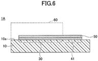
- FIG. 6 is a cross-sectional view illustrating a strain gauge according to the third embodiment, which illustrates a cross section corresponding to FIG. 2 .
- a strain gauge 1A is provided with an oxidation impeding layer 50 on the upper surfaces of the resistor 30 and the terminal sections 41, and in this regard, differs from the strain gauge 1 (see FIGs. 1 and 2 ).
- the resistance value and the gauge factor of a thin film containing Cr as a base depend on the oxidation state. Therefore, the oxidation control of Cr is important; however, the oxide layer of Cr easily forms an oxide layer as generally called a passive layer, and thereby, it is difficult to control the oxidation.
- the oxidation impeding layer 50 is provided on the upper surfaces of the resistor 30 and the terminal sections 41. However, depending on the conductivity of the oxidation impeding layer 50, the oxidation impeding layer 50 on the upper surfaces of the terminal sections 41 may be removed.
- the material of the oxidation impeding layer 50 is not limited in particular as long as being capable of preventing oxidation of the resistor 30, and can be selected appropriately depending on the purpose; Ti, TiN, TaN, Si 3 O 4 , Si, SiO 2 , ZrO 2 , or the like may be listed. Multiple species of substances selected from among these may be mixed.
- the thickness of the oxidation impeding layer 50 is approximately 1 nm to 100 nm, from the viewpoint of reducing the influence on the gauge characteristics of the Cr composite film.
- the thickness of the oxidation impeding layer 50 is approximately 1 nm to 10 nm, from the viewpoint of improving the stability of TCR of the Cr composite film.
- an oxidation impeding layer 50 on the upper surfaces of the resistor 30 and the terminal sections 41 In order to form an oxidation impeding layer 50 on the upper surfaces of the resistor 30 and the terminal sections 41, after having the resistor 30 and the terminal sections 41 formed, a film is formed in vacuum on the entire upper surfaces of the resistor 30 and the terminal sections 41, for example, by a conventional sputtering method using a raw material that is capable of forming an oxidation impeding layer 50 as a target, and introducing Ar (argon) gas into the chamber. Thereafter, the resistor 30, the terminal sections 41, and the oxidation impeding layer 50 are patterned into a planar shape as illustrated in FIG. 1 . Thereafter, if necessary, the oxidation impeding layer 50 on the upper surfaces of the terminal sections 41 is removed.
- Ar argon
- the film formation of the resistor 30 and the terminal sections 41, and the film formation of the oxidation impeding layer 50 as a series of steps in a vacuum chamber it is possible to form the oxidation impeding layer 50 directly on the upper surface of the resistor 30, without forming an oxide layer on the upper surfaces of the resistor 30 and the terminal sections 41. In other words, it is possible to form an oxidation impeding layer 50 on a non-oxidized surface, which corresponds to the upper surfaces of the resistor 30 and the terminal sections 41.
- the patterning causes the side surfaces of the resistor 30 and the terminal sections 41 to be exposed from the oxidation impeding layer 50, the resistor 30 and the terminal sections 41 are thin, and the area of the side surfaces is small; therefore, oxidation from the side surfaces does not pose a problem.
- an oxidation impeding layer 50 as a film on the non-oxidized surface corresponding to the upper surface of the resistor 30, even in the case of the resistor 30 being a thin film containing Cr as a base, the resistor 30 is not oxidized; therefore, it is possible to improve the stability of the resistance value of the resistor 30 and the gauge factor of the strain gauge 1A. Also, it is possible to further improve the stability of the TCR of the strain gauge 1A.
- the functional layer it is favorable to provide a functional layer as an underlayer of the resistor 30.
- the functional layer it is favorable to use a layer that has a function of promoting the crystal growth of the resistor 30 as the upper layer, and a function of preventing oxidation of the resistor 30 due to oxygen and moisture contained in the substrate 10.
- the functional layer serves as a barrier layer to control oxidation of the resistor 30 from the substrate 10 side; therefore, it is possible to further improve the stability of the resistance value of the resistor 30 and the gauge factor of the strain gauge 1A. In addition, it is possible to further improve the stability of the TCR of the strain gauge 1A.
- the resistor 30 being a Cr composite film
- Ti and TiN may be listed, and it is particularly favorable to use TiN.
- diffusing Ti into a Cr-composite film improves the gauge characteristics, but causes variations in the gauge characteristics depending on the degree of diffusion; however, in the case of diffusing TiN into a Cr composite film, the degree of diffusion in the Cr composite film is smaller; therefore, variations in the gauge characteristics depending on the degree of diffusion are less likely to occur, and thereby, the stability of the gauge characteristics depending on the temperature is improved.
- the first embodiment and the third embodiment can be combined.
- the resistor 30 being a Cr composite film
- a functional layer of TiN or the like having a function of promoting crystal growth of the resistor 30 and a function of preventing oxidation of the resistor 30 may be provided as an underlayer of the resistor 30. This enables to obtain both of the effects described in the first embodiment and in the second embodiment.
- the second embodiment and the third embodiment can be combined.
- the resistor 30 being a Cr composite film
- a functional layer of TiN or the like having a function of promoting crystal growth of the resistor 30 and a function of preventing oxidation of the resistor 30 may be provided as an underlayer of the resistor 30. This enables to obtain both of the effects described in the second embodiment and in the third embodiment.
- the first embodiment, the second embodiment, and the third embodiment can be combined.
- the resistor 30 being a Cr composite film
- a functional layer of TiN or the like having a function of promoting crystal growth of the resistor 30 and a function of preventing oxidation of the resistor 30 may be provided as an underlayer of the resistor 30. This enables to obtain all of the effects described in the first embodiment, the second embodiment, and the third embodiment.
- the same effects as in the case of the thin film containing Cr as a base can be obtained in the case of a Cu-Ni thin film or a Ni-Cr thin film, by providing an oxidation impeding layer 50 on the upper surface of the resistor 30. Also, for a Cu-Ni thin film and a Ni-Cr thin film, by providing, as an underlayer of the resistor 30, a functional layer having a function of promoting crystal growth and a function of serving as a barrier layer, the same effects as in the case of the thin film containing Cr as a base can be obtained.
Landscapes
- Physics & Mathematics (AREA)
- General Physics & Mathematics (AREA)
- Measurement Of Length, Angles, Or The Like Using Electric Or Magnetic Means (AREA)
- Non-Adjustable Resistors (AREA)
Abstract
Description
- The present invention relates to a strain gauge.
- Strain gauges that have been known are attached to an object to be measured so as to detect a strain of the object. Such a strain gauge includes a resistor for detecting a strain, and as materials of the resistor, materials containing, for example, Cr (chromium) and/or Ni (nickel) are used. Also, the resistor is formed in a predetermined pattern, for example, by etching a metal foil (see, e.g., Patent Document 1).
- [Patent Document 1] Japanese Unexamined Patent Application Publication No.
2016-74934 - However, in the case of using a substrate having flexibility, it is difficult to form a stable resistor on the substrate, and there has been a problem that such a strain gauge lacks stability in the gauge characteristics, especially in the temperature coefficient of resistance TCR.
- The present invention has been made in view of the above points, and has an object to improve the stability of the temperature coefficient of resistance TCR in a strain gauge.
- The present strain gauge includes a substrate having flexibility; and a resistor formed from a material containing at least one of chromium and nickel, on the substrate, wherein a first substance having a function of controlling growth of crystal grains as the main component of the resistor, is added to the resistor.
- According to the disclosed technique, it is possible to improve the stability of the temperature coefficient of resistance TCR in a strain gauge.
-
-
FIG. 1 is a plan view illustrating a strain gauge according to a first embodiment; -
FIG. 2 is a first cross-sectional view illustrating a strain gauge according to the first embodiment; -
FIG. 3 is a first schematic view illustrating the inside of a resistor in the case where the resistor is a Cr composite film; -
FIG. 4 is a second cross-sectional view illustrating a strain gauge according to the first embodiment; -
FIG. 5 is a second schematic view illustrating the inside of a resistor in the case where the resistor is a Cr composite film; and -
FIG. 6 is a cross-sectional view illustrating a strain gauge according to a third embodiment. - In the following, embodiments for carrying out the present invention will be described with reference to the drawings. Throughout the drawings, the same elements are assigned the same reference numerals, and duplicate description may be omitted.
-
FIG. 1 is a plan view illustrating a strain gauge according to a first embodiment.FIG. 2 is a cross-sectional view illustrating the strain gauge according to the first embodiment, which illustrates a cross section taken along a line AA inFIG. 1 . Referring toFIGs. 1 and 2 , astrain gauge 1 includes asubstrate 10, aresistor 30, andterminal sections 41. - Note that in the present embodiment, for the sake of convenience, a side of the
strain gauge 1 on which theresistor 30 of thesubstrate 10 is provided is defined as an upper side or one side, and another side on which theresistor 30 is not provided is defined as a lower side or the other side. Also, a surface of each part on which theresistor 30 is provided is defined as one surface or upper surface, and another surface on which theresistor 30 is not provided is defined as the other surface or lower surface. However, thestrain gauge 1 can be used upside down, or can be arranged at any angle. Also, a plan view refers to viewing an object from the normal direction of theupper surface 10a of thesubstrate 10, and a planar shape refers to a shape of an object viewed from the normal direction of theupper surface 10a of thesubstrate 10. - The
substrate 10 is a member serving as a base layer for forming theresistor 30 and the like, and has flexibility. The thickness of thesubstrate 10 is not limited in particular and can be selected appropriately depending on the purpose; for example, the thickness can be approximately 5 µm to 500 µm. Especially, it is favorable that the thickness of thesubstrate 10 is between 5 µm and 200 µm from the viewpoint of the transmission of strain from the surface of the strain generator joined to the lower surface of thesubstrate 10 via an adhesive layer or the like, and the dimensional stability with respect to the environment; and it is more favorable that the thickness is greater than or equal to 10 µm from the viewpoint of insulation. - The
substrate 10 can be formed from an insulating resin film, for example, PI (polyimide) resin, epoxy resin, PEEK (polyether ether ketone) resin, PEN (polyethylene naphthalate) resin, PET (polyethylene terephthalate) resin, PPS (polyphenylene sulfide) resin, polyolefin resin, or the like. Note that a film refers to a member having a thickness of approximately less than or equal to 500 µm and having flexibility. - Here, "formed from an insulating resin film" does not preclude a
substrate 10 from containing fillers, impurities, and the like in the insulating resin film. Thesubstrate 10 may be formed from, for example, an insulating resin film containing a filler such as silica or alumina. - The
resistor 30 is a thin film formed on thesubstrate 10 to have a predetermined pattern, which is a sensing part in which a resistance change is generated in response to a strain. Theresistor 30 may be formed directly on theupper surface 10a of thesubstrate 10, or may be formed on theupper surface 10a of thesubstrate 10 via another layer. Note that inFIG. 1 , theresistor 30 is illustrated in a dot pattern for the sake of convenience. - The
resistor 30 can be formed from, for example, a material containing Cr (chromium), a material containing Ni (nickel), or a material containing both Cr and Ni. In other words, theresistor 30 can be formed from a material containing at least one of Cr and Ni. As an example of the material containing Cr, for example, a Cr composite film may be cited. As an example of the material containing Ni, for example, Cu-Ni (copper-nickel) may be cited. As a material containing both Cr and Ni, for example, Ni-Cr (nickel-chrome) may be cited. - Here, the Cr composite film is a film in which Cr, CrN, Cr2N, and the like are mixed. The Cr composite film may contain unavoidable impurities such as chromium oxide.
- The thickness of the
resistor 30 is not limited in particular and can be selected appropriately depending on the purpose; for example, the thickness can be approximately 0.05 µm to 2 µm. Especially, it is favorable that the thickness of theresistor 30 is greater than or equal to 0.1 µm because the crystallinity of crystals constituting the resistor 30 (e.g., the crystallinity of α-Cr) improves, and it is further favorable that the thickness is less than or equal to 1 µm because cracks in the film and/or the warp from thesubstrate 10 due to the internal stress of the film constituting theresistor 30 can be reduced. - For example, in the case of the
resistor 30 being a Cr composite film, the stability of the gauge characteristics can be improved by using α-Cr (alpha chromium), which is a stable crystal phase, as the main component. Also, by having theresistor 30 mainly constituted with α-Cr, the gauge factor of thestrain gauge 1 can be greater than or equal to 10, and the temperature coefficient of gauge factor TCS and the temperature coefficient of resistance TCR can be fallen within a range of -1000 ppm/°C to +1000 ppm/°C. Here, the main component means that a substance accounts for greater than or equal to 50 mass% among all substances constituting the resistor; from the viewpoint of improving the gauge characteristics, it is favorable that theresistor 30 contains α-Cr by greater than or equal to 80 wt%. Note that α-Cr is Cr having a bcc structure (body-centered cubic lattice structure). -
FIG. 3 is a schematic view illustrating the inside of a resistor in the case where the resistor is a Cr composite film, which schematically illustrates states before and after heating. As illustrated inFIG. 3 , theresistor 30 as a Cr composite film includes α-Cr crystal grains 301 and chromium nitride 302 (one or both of CrN and Cr2N); and in the present embodiment, asubstance 303 is further added. - In a Cr composite film to which the
substance 303 is not added, the TCR changes greatly by heating, and a longer heating time makes the TCR greater in the positive direction. This is because the crystal grains of Cr as a positive component of TCR gradually grow by heating, and the chromium nitride as a negative component of TCR present in the crystal grain boundaries is taken into the Cr film or pushed out to the outside, and thereby, the chromium nitride present in the crystal grain boundaries becomes reduced. Therefore, as the heating time becomes longer, the TCR continues to increase to be a greater positive value. - Thereupon, in the present embodiment, a
substance 303 that controls the growth of α-Cr crystal grains 301 is added to the Cr composite film, and thesubstance 303 is dispersed in the Cr composite film. - The
substance 303 is not limited in particular and can be selected appropriately depending on the purpose as long as being a substance that has a function of controlling the growth of α-Cr crystal grains 301. It is favorable that thesubstance 303 has a TCR of greater than or equal to - 30000 ppm/°C and less than or equal to +1000 ppm/°C, and an electric conductivity of greater than 10-6 S/m and less than or equal to 107 S/m; for example, a metal compound such as TiN, TaN, SiTiN, or CrSiO, or a semiconductor such as Si may be listed. Multiple species of substances selected from among these may be mixed. - Here, the reason why the TCR is favorably greater than or equal to -30000ppm/°C and less than or equal to +1000 ppm/°C is as follows. For example, in the case where a substance having a TCR greater than +1000 ppm/°C is present in the crystal grain boundaries, the behavior as a conductor becomes dominant; therefore, the TCR value of the entire film becomes greater than +1000 ppm/°C. Also, in the case where a substance having a TCR smaller than -30000 ppm/°C is present in the crystal grain boundaries, due to the contribution of thermally activated hopping conduction caused by structural defects, the TCR value becomes unstable. In contrast, in the case where a
substance 303 having a TCR of greater than or equal to -30000 ppm/°C and less than or equal to +1000 ppm/°C is present in the crystal grain boundaries, the problems described above do not occur; therefore, it is possible to stably control the TCR of the entire Cr composite film to a low value. - Also, the reason why the electric conductivity is favorably greater than 10-6 S/m and less than or equal to 107 S/m is as follows. For example, in the case of adding a metal as a substance whose electric conductivity is greater than 107 S/m to a Cr composite film, the TCR changes significantly because the metal diffuses into the Cr composite film by heating. Also, in the case of adding a substance of less than or equal to 10-6 S/m, it is not possible to control the electric properties in the Cr composite film because it hardly conducts electricity. On the other hand, in the case of adding the
substance 303 having an electric conductivity of greater than 10-6 S/m and less than or equal to 107 S/m to the Cr composite film, diffusion can be controlled unlike a metal; in addition, a material having electrical characteristics in accordance with the characteristics of the Cr composite film can be added; therefore, the TCR can be maintained to be a low value both before and after the heating. - The amount of the
substance 303 to be added can be appropriately selected depending on the film-forming conditions of theresistor 30, and can be 1 to 25 wt%. It is particularly favorable that the added amount of thesubstance 303 in theresistor 30 is 2 to 10 wt% because the crystallinity of α-Cr is improved. - By adding the
substance 303, which has a function of controlling the growth of α-Cr crystal grains 301, to theresistor 30 as a Cr composite film, it is possible to prevent the TCR from continuously increasing as a positive value due to heating, and to control the TCR to be a low value. In other words, it is possible to further improve the stability of the TCR of thestrain gauge 1. Note that depending on the amount of thesubstance 303 added to the Cr composite film, it is possible to control the growth rate of α-Cr crystal grains 301, and consequently, to control the TCR of thestrain gauge 1. - As above, although the description has been made taking a Cr composite film as an example, the same effects as in the case of the Cr composite film can be obtained in the case of a Cu-Ni thin film or a Ni-Cr thin film, by adding to the resistor a substance that has a function of controlling growth of crystal grains as the main component of the resistor.
- Referring back to
FIGs. 1 and 2 , theterminal section 41 extends from both ends of theresistor 30, and is formed in a substantially rectangular shape having a wider width than theresistor 30 in plan view. Theterminal sections 41 are a pair of electrodes for outputting to the outside a change in the resistance value of theresistor 30 caused by a strain, to which, for example, lead wires or the like for external connection are joined. Theresistor 30 extends, for example, in a zigzag way from one of theterminal sections 41 and is connected to the other of theterminal sections 41. The upper surfaces of theterminal sections 41 may be covered with a metal having better solderability than theterminal sections 41. Note that although different numerals are used for theresistor 30 and theterminal sections 41 for the sake of convenience, these may be integrally formed of the same material in the same process. - A cover layer 60 (an insulating resin layer) may be provided on the
substrate 10, so as to cover theresistor 30. By providing thecover layer 60, it is possible to prevent mechanical damage and the like from occurring in theresistor 30. Also, by providing thecover layer 60, it is possible to protect theresistor 30 from moisture and the like. Note that thecover layer 60 may be provided so as to cover the entire part excluding theterminal sections 41. - The
cover layer 60 can be formed from an insulating resin; for example, PI resin, epoxy resin, PEEK resin, PEN resin, PET resin, PPS resin, composite resin (e.g., silicone resin, polyolefin resin), or the like. Thecover layer 60 may contain a filler or a pigment. The thickness of thecover layer 60 is not limited in particular and can be selected appropriately depending on the purpose; for example, the thickness can be approximately 2 µm to 30 µm. - In order to manufacture a
strain gauge 1, first, asubstrate 10 is prepared, and aplanar resistor 30 and aterminal sections 41 as illustrated inFIG. 1 are formed on theupper surface 10a of thesubstrate 10. The material and thickness of theresistor 30 and theterminal sections 41 are as described above. Theresistor 30 and theterminal sections 41 can be integrally formed of the same material. - The
resistor 30 and theterminal sections 41 can be formed by, for example, forming a film by a magnetron sputtering method using a material capable of forming theresistor 30 and theterminal sections 41 as a target; and patterning the formed film by photolithography. Theresistor 30 and theterminal sections 41 may be formed using a reactive sputtering method, an evaporation method, an arc ion plating method, a pulse laser deposition method, or the like instead of the magnetron sputtering method. - From the viewpoint of stabilizing the gauge characteristics, before forming the
resistor 30 and theterminal sections 41 as a film, as an underlayer, it is favorable to form in vacuum a functional layer having a thickness of approximately 1 nm to 100 nm on theupper surface 10a of thesubstrate 10 by, for example, a conventional sputtering method. Note that after having theresistor 30 and theterminal sections 41 formed on the entire upper surface of the functional layer, the functional layer is patterned by photolithography together with theresistor 30 and theterminal sections 41 into a planar shape as illustrated inFIG. 1 . - In the present application, the functional layer refers to a layer having a function of promoting crystal growth of at least the
resistor 30 as the upper layer. It is favorable that the functional layer further has a function of preventing oxidation of theresistor 30 due to oxygen and moisture contained in thesubstrate 10, and a function of improving the adhesion between thesubstrate 10 and theresistor 30. The functional layer may further have other functions. - The insulating resin film constituting the
substrate 10 contains oxygen and moisture, and thereby, especially when theresistor 30 contains Cr, Cr forms a self-oxidized film; therefore, it is effective that the functional layer has a function of preventing oxidation of theresistor 30. - The material of the functional layer is not limited in particular as long as it has a function of promoting crystal growth of at least the
resistor 30 as the upper layer, and can be appropriately selected depending on the purpose; as the material, one or more species of metals selected from among a group consisting of, for example, Cr (chromium), Ti (titanium), V (vanadium), Nb (niobium), Ta (tantalum), Ni (nickel), Y (yttrium), Zr (zirconium), Hf (hafnium), Si (silicon), C (carbon), Zn (zinc), Cu (copper), Bi (bismuth), Fe (iron), Mo (molybdenum), W (tungsten), Ru (ruthenium), Rh (rhodium), Re (rhenium), Os (osmium), Ir (iridium), Pt (platinum), Pd (palladium), Ag (silver), Au (gold), Co (cobalt), Mn (manganese), and Al (aluminum); an alloy of any of the metals in this group; or a compound of any of the metals in this group may be listed. - As examples of the alloys described above, FeCr, TiAl, FeNi, NiCr, CrCu, and the like may be listed. Also, as examples of the compounds described above, TiN, TaN, Si3N4, TiO2, Ta2O5, SiO2, and the like may be listed.
- The functional layer can be formed by, for example, a conventional sputtering method using a material capable of forming the functional layer as a target, and introducing Ar (argon) gas into the chamber. By using the conventional sputtering method, the functional layer is formed as a film while the
upper surface 10a of thesubstrate 10 is being etched with Ar; therefore, the effect of improving the adhesion can be obtained by minimizing the amount of the functional layer formed as a film. - However, this is an example of the method of forming a functional layer as a film, and the functional layer may be formed by another method. For example, a method may be used in which the
upper surface 10a of thesubstrate 10 is activated by plasma treatment using Ar or the like before forming the functional layer so as to obtain an adhesion improving effect, and then, the functional layer is formed in vacuum as a film by a magnetron sputtering method. - The combination of the material of the functional layer and the material of the
resistor 30 and theterminal sections 41 is not limited in particular and can be appropriately selected depending on the purpose; for example, it is possible to use Ti as the functional layer, and to form a Cr composite film containing α-Cr (alpha chromium) as the main component, as theresistor 30 and theterminal sections 41. - In this case, for example, the
resistor 30 and theterminal sections 41 can be formed as a film by a magnetron sputtering method using a material capable of forming a Cr composite film as a target, and introducing Ar gas into the chamber. Alternatively, theresistor 30 and theterminal sections 41 may be formed as a film by a reactive sputtering method using pure Cr as a target, and introducing an appropriate amount of nitrogen gas together with Ar gas into the chamber. - In these methods, a growth face of the Cr mixed-phase film is defined and triggered by the functional layer formed of Ti, which enables to form a Cr composite film containing, as the main component, α-Cr having a stable crystal structure. Also, the gauge characteristics are improved by Ti constituting the functional layer diffusing into the Cr composite film. For example, the gauge factor of the
strain gauge 1 can be greater than or equal to 10, and the temperature coefficient of gauge factor TCS and the temperature coefficient of resistance TCR can be fallen within a range of -1000 ppm/°C to +1000 ppm/°C. Note that in the case of forming the functional layer from Ti, the Cr composite film may contain Ti or TiN. In other words, it is possible to add TiN to a Cr composite film from a functional layer made of Ti. - Note that in the case where the
resistor 30 is a Cr composite film, the functional layer made of Ti has all of the function of promoting the crystal growth of theresistor 30; the function of preventing oxidation of theresistor 30 due to oxygen and moisture contained in thesubstrate 10; and the function of improving the adhesion between thesubstrate 10 and theresistor 30. The same applies in the case of using Ta, Si, Al, or Fe instead of Ti as the functional layer. - In this way, by providing a functional layer as an underlayer of the
resistor 30, the crystal growth of theresistor 30 can be promoted, and theresistor 30 having a stable crystal phase can be manufactured. As a result, the stability of the gauge characteristics of thestrain gauge 1 can be improved. Also, by diffusing the material constituting the functional layer into theresistor 30, the gauge characteristics of thestrain gauge 1 can be improved. - Also, in order to form a Cr composite film having TiN added, a
resistor 30 andterminal sections 41 may be formed as a film by a reactive sputtering method using Cr and Ti as respective targets, and introducing an appropriate amount of nitrogen gas together with Ar gas into the chamber. In this case, Ti is formed as TiN in the Cr composite film, and thus, a Cr composite film having TiN added can be formed. - Note that in this method, by forming a Cr composite film on a functional layer other than Ti, a Cr composite film having TiN added can be formed. Also, in this method, by forming a Cr composite film directly on the
upper surface 10a of thesubstrate 10, without having formed a functional layer, a Cr composite film having TiN added can be formed. - After having the
resistor 30 and theterminal sections 41 formed, if necessary, by providing acover layer 60 on theupper surface 10a of thesubstrate 10, so as to cover theresistor 30 and to expose theterminal sections 41, thestrain gauge 1 is completed. Thecover layer 60 can be manufactured, for example, by laminating a thermosetting insulating resin film in a semi-cured state on theupper surface 10a of thesubstrate 10, so as to cover theresistor 30 and to expose theterminal sections 41, and heating the laminated film to be cured. Thecover layer 60 may also be manufactured by applying a liquid or paste-like thermosetting insulating resin to theupper surface 10a of thesubstrate 10, so as to cover theresistor 30 and to expose theterminal sections 41, and heating the resin to be cured. - Note that in the case of providing the functional layer on the
upper surface 10a of thesubstrate 10 as the underlayer of theresistor 30 and theterminal section 41, thestrain gauge 1 has a cross-sectional shape illustrated inFIG. 4 . A layer indicated by areference numeral 20 is the functional layer. The planar shape of thestrain gauge 1 in the case of providing thefunctional layer 20 is the same as that inFIG. 1 . - In the second embodiment, an example will be described in which a substance having characteristics different from those of the first embodiment is added to the resistor. Note that in the second embodiment, description of the same components as those already described may be omitted.
-
FIG. 5 is a schematic view illustrating the inside of a resistor in the case where the resistor is a Cr composite film. As illustrated inFIG. 5 , theresistor 30 as a Cr composite film includes α-Cr crystal grains 301 and chromium nitride 302 (one or both of CrN and Cr2N); in the present embodiment, asubstance 304 is further added. - The TCR of the Cr composite film before heating to which the
substance 304 is not added exhibits a negative value. This is because although the crystal grains of Cr are a positive component of TCR, for example, due to the film formation in a nitrogen atmosphere, chromium nitride (one or both of CrN and Cr2N) as a negative component of TCR is formed in the crystal grain boundaries of Cr, and the effect of chromium nitride as a negative component of TCR becomes apparent noticeably. - In a Cr composite film to which the
substance 304 is not added, the TCR changes greatly by heating, and the TCR of Cr composite film exhibits a low value. This is because the residual stress in the Cr composite film is alleviated, the crystal grains of Cr come closer to each other, and thereby, the tunnel current in the crystal grain boundaries becomes greater, and the effect of chromium nitride as a negative component of TCR is reduced. - In the present embodiment, the
substance 304 that has a function of preventing α-Cr crystal grains 301 from cohering is added to the Cr composite film, and thesubstance 304 is dispersed in the Cr composite film and present in the crystal grain boundaries of the α-Cr crystal grains 301. - The
substance 304 is not limited in particular and can be selected appropriately depending on the purpose as long as being a substance that has a function of preventing α-Cr crystal grains 301 from cohering. It is favorable that thesubstance 304 has a TCR of greater than or equal to - 30000ppm/°C and less than or equal to +1000ppm/°C, and an electric conductivity of less than or equal to 10-6 S/m; for example, an insulator such as AlN, BN, TiO2, ZrO2, SiO2, or Si3N4 may be listed. Multiple species of substances selected from among these may be mixed. - Here, the reason why the TCR is favorably greater than or equal to -30000ppm/°C and less than or equal to +1000 ppm/°C is as follows. For example, in the case where a substance having a TCR greater than +1000 ppm/°C is present in the crystal grain boundaries, the behavior as a conductor becomes dominant; therefore, the TCR value of the entire film becomes greater than +1000 ppm/°C. Also, in the case where a substance having a TCR smaller than -30000 ppm/°C is present in the crystal grain boundaries, due to the contribution of thermally activated hopping conduction caused by structural defects, the TCR value becomes unstable. In contrast, in the case where a
substance 304 having a TCR of greater than or equal to -30000 ppm/°C and less than or equal to +1000 ppm/°C is present in the crystal grain boundaries, the problems described above do not occur; therefore, it is possible to stably control the TCR of the entire Cr composite film to a low value. - Also, the reason why the electric conductivity is favorably less than or equal to 10-6 S/m is as follows. For example, in the case of adding a metal as a substance whose electric conductivity is greater than 107 S/m to a Cr composite film, the TCR changes significantly because the metal diffuses into the Cr composite film by heating. Also, in the case of adding a metal compound having higher electrical properties than an insulator, as a substance having an electrical conductivity of greater than 10-6 S/m and less than or equal to 107 S/m in a Cr composite film, unlike metal, diffusion can be controlled, but changes in the electrical characteristics of the Cr composite are induced. In contrast, in the case of adding the
substance 304 having an electrical conductivity of less than or equal to 10-6 S/m in a Cr composite film, unlike metal, diffusion is controlled, and the distance between Cr particles can be controlled; therefore, the TCR can be maintained to have a low value both before and after heating. - The amount of the
substance 304 to be added can be appropriately selected depending on the film-forming conditions of theresistor 30, which can be 1 to 25 wt%. It is particularly favorable that the added amount of thesubstance 304 in theresistor 30 is 2 to 10 wt% because the crystallinity of α-Cr is improved. - By adding a
substance 304, which has a function of preventing α-Cr crystal grains 301 from cohering, to theresistor 30 as a Cr composite film so as to have thesubstance 304 present in the crystal grain boundaries, it is possible to control cohesion between crystal grains of Cr as a positive component of TCR, and to lower the TCR of the strain gauge. - In other words, the
substance 304 present in the crystal grain boundaries prevents the α-Cr crystal grains 301 from cohering due to alleviation of residual stress during heating; therefore, even after the heating, the state inside theresistor 30 is not significantly different from the state before the heating, and thereby, the TCR of thestrain gauge 1 can be maintained at a low value. - As a result, it is possible to maintain the TCR of the Cr composite film at a low value both before and after the heating, and to control the change in the TCR before and after the heating. In other words, it is possible to further improve the stability of the TCR of the
strain gauge 1. Note that depending on the amount ofsubstance 304 added to the Cr composite film, it is possible to control the degree of proximity between α-Cr crystal grains 301, and consequently, to control the TCR of thestrain gauge 1. - In order to form a Cr composite film to which AlN is added, for example, a functional layer made of Al is formed as a film on the
upper surface 10a of thesubstrate 10. Then, theresistor 30 and theterminal sections 41 can be formed as a film by a magnetron sputtering method using a raw material capable of forming a Cr composite film as a target and introducing Ar gas into the chamber. Alternatively, theresistor 30 and theterminal sections 41 may be formed as a film by a reactive sputtering method using pure Cr as a target, and introducing an appropriate amount of nitrogen gas together with Ar gas into the chamber. - In these methods, a growth face of the Cr mixed-phase film is defined and triggered by the functional layer formed of Al, which enables to form a Cr composite film containing, as the main component, α-Cr having a stable crystal structure. Also, the gauge characteristics are improved by Al constituting the functional layer diffusing into the Cr composite film. For example, the gauge factor of the
strain gauge 1 can be greater than or equal to 10, and the temperature coefficient of gauge factor TCS and the temperature coefficient of resistance TCR can be fallen within a range of -1000 ppm/°C to +1000 ppm/°C. Note that in the case of forming the functional layer from Al, the Cr composite film may contain Al or AlN. In other words, it is possible to add AlN to a Cr composite film from a functional layer made of Al. - Also, in order to form a Cr composite film having AlN added, a
resistor 30 andterminal sections 41 may be formed as a film by a reactive sputtering method using Cr and Al as respective targets, and introducing an appropriate amount of nitrogen gas together with Ar gas into the chamber. In this case, Al is formed as AlN in the Cr composite film, and thus, a Cr composite film having AlN added can be formed. - Note that in this method, by forming a Cr composite film on a functional layer other than Al, a Cr composite film having AlN added can be formed. Also, in this method, by forming a Cr composite film directly on the
upper surface 10a of thesubstrate 10, without having formed a functional layer, a Cr composite film having AlN added can be formed. - The first embodiment and the second embodiment can be combined. For example, in the case of the
resistor 30 being a Cr composite film, it is possible to add TiN as thesubstance 303 and AlN as thesubstance 304 to theresistor 30. This enables to obtain both of the effects described in the first embodiment and in the second embodiment. - As above, although the description has been made taking a Cr composite film as an example, the same effects as in the case of the Cr composite film can be obtained in the case of a Cu-Ni thin film or a Ni-Cr thin film, by adding to the resistor a substance that has a function of preventing crystal grains as the main component of the resistor from cohering.
- In the third embodiment, an example will be described in which the stability of the TCR of a strain gauge is improved by a method different from those of the first and second embodiments. Note that in the third embodiment, description of the same components as those already described may be omitted.
-
FIG. 6 is a cross-sectional view illustrating a strain gauge according to the third embodiment, which illustrates a cross section corresponding toFIG. 2 . Referring toFIG. 6 , astrain gauge 1A is provided with anoxidation impeding layer 50 on the upper surfaces of theresistor 30 and theterminal sections 41, and in this regard, differs from the strain gauge 1 (seeFIGs. 1 and 2 ). - The resistance value and the gauge factor of a thin film containing Cr as a base depend on the oxidation state. Therefore, the oxidation control of Cr is important; however, the oxide layer of Cr easily forms an oxide layer as generally called a passive layer, and thereby, it is difficult to control the oxidation. Thereupon, in the present embodiment, as illustrated in
FIG. 6 , theoxidation impeding layer 50 is provided on the upper surfaces of theresistor 30 and theterminal sections 41. However, depending on the conductivity of theoxidation impeding layer 50, theoxidation impeding layer 50 on the upper surfaces of theterminal sections 41 may be removed. - The material of the
oxidation impeding layer 50 is not limited in particular as long as being capable of preventing oxidation of theresistor 30, and can be selected appropriately depending on the purpose; Ti, TiN, TaN, Si3O4, Si, SiO2, ZrO2, or the like may be listed. Multiple species of substances selected from among these may be mixed. - For example, in the case of the
resistor 30 being a Cr composite film, and the material of theoxidation impeding layer 50 being Ti, it is favorable that the thickness of theoxidation impeding layer 50 is approximately 1 nm to 100 nm, from the viewpoint of reducing the influence on the gauge characteristics of the Cr composite film. Also, in the case of theresistor 30 being a Cr composite film, and the material of theoxidation impeding layer 50 being TiN, it is favorable that the thickness of theoxidation impeding layer 50 is approximately 1 nm to 10 nm, from the viewpoint of improving the stability of TCR of the Cr composite film. - In order to form an
oxidation impeding layer 50 on the upper surfaces of theresistor 30 and theterminal sections 41, after having theresistor 30 and theterminal sections 41 formed, a film is formed in vacuum on the entire upper surfaces of theresistor 30 and theterminal sections 41, for example, by a conventional sputtering method using a raw material that is capable of forming anoxidation impeding layer 50 as a target, and introducing Ar (argon) gas into the chamber. Thereafter, theresistor 30, theterminal sections 41, and theoxidation impeding layer 50 are patterned into a planar shape as illustrated inFIG. 1 . Thereafter, if necessary, theoxidation impeding layer 50 on the upper surfaces of theterminal sections 41 is removed. - By performing the film formation of the
resistor 30 and theterminal sections 41, and the film formation of theoxidation impeding layer 50 as a series of steps in a vacuum chamber, it is possible to form theoxidation impeding layer 50 directly on the upper surface of theresistor 30, without forming an oxide layer on the upper surfaces of theresistor 30 and theterminal sections 41. In other words, it is possible to form anoxidation impeding layer 50 on a non-oxidized surface, which corresponds to the upper surfaces of theresistor 30 and theterminal sections 41. - Note that although the patterning causes the side surfaces of the
resistor 30 and theterminal sections 41 to be exposed from theoxidation impeding layer 50, theresistor 30 and theterminal sections 41 are thin, and the area of the side surfaces is small; therefore, oxidation from the side surfaces does not pose a problem. - In this way, by forming an
oxidation impeding layer 50 as a film on the non-oxidized surface corresponding to the upper surface of theresistor 30, even in the case of theresistor 30 being a thin film containing Cr as a base, theresistor 30 is not oxidized; therefore, it is possible to improve the stability of the resistance value of theresistor 30 and the gauge factor of thestrain gauge 1A. Also, it is possible to further improve the stability of the TCR of thestrain gauge 1A. - Note that as in the first and second embodiments, it is favorable to provide a functional layer as an underlayer of the
resistor 30. In the present embodiment, as the functional layer, it is favorable to use a layer that has a function of promoting the crystal growth of theresistor 30 as the upper layer, and a function of preventing oxidation of theresistor 30 due to oxygen and moisture contained in thesubstrate 10. - This enables to promote the crystal growth of the
resistor 30, to manufacture theresistor 30 having a stable crystal phase, and to improve the stability of the gauge characteristics. Also, diffusing the material forming the functional layer into theresistor 30 enables to improve the gauge characteristics. Furthermore, the functional layer serves as a barrier layer to control oxidation of theresistor 30 from thesubstrate 10 side; therefore, it is possible to further improve the stability of the resistance value of theresistor 30 and the gauge factor of thestrain gauge 1A. In addition, it is possible to further improve the stability of the TCR of thestrain gauge 1A. - For example, in the case of the
resistor 30 being a Cr composite film, as the functional layer having a function of promoting crystal growth and a function of serving as a barrier layer, Ti and TiN may be listed, and it is particularly favorable to use TiN. The reason why is as follows: diffusing Ti into a Cr-composite film improves the gauge characteristics, but causes variations in the gauge characteristics depending on the degree of diffusion; however, in the case of diffusing TiN into a Cr composite film, the degree of diffusion in the Cr composite film is smaller; therefore, variations in the gauge characteristics depending on the degree of diffusion are less likely to occur, and thereby, the stability of the gauge characteristics depending on the temperature is improved. - The first embodiment and the third embodiment can be combined. For example, in the case of the
resistor 30 being a Cr composite film, it is possible to add TiN as thesubstance 303 to theresistor 30, and to form a film of Ti on the upper surface of theresistor 30 as anoxidation impeding layer 50. Furthermore, a functional layer of TiN or the like having a function of promoting crystal growth of theresistor 30 and a function of preventing oxidation of theresistor 30 may be provided as an underlayer of theresistor 30. This enables to obtain both of the effects described in the first embodiment and in the second embodiment. - Also, the second embodiment and the third embodiment can be combined. For example, in the case of the
resistor 30 being a Cr composite film, it is possible to add AlN as thesubstance 304 to theresistor 30, and to form a film of Ti on the upper surface of theresistor 30 as anoxidation impeding layer 50. Furthermore, a functional layer of TiN or the like having a function of promoting crystal growth of theresistor 30 and a function of preventing oxidation of theresistor 30 may be provided as an underlayer of theresistor 30. This enables to obtain both of the effects described in the second embodiment and in the third embodiment. - Also, the first embodiment, the second embodiment, and the third embodiment can be combined. For example, in the case of the
resistor 30 being a Cr composite film, it is possible to add TiN as thesubstance 303 and AlN as thesubstance 304 to theresistor 30, and to form a film of Ti on the upper surface of theresistor 30 as anoxidation impeding layer 50. Furthermore, a functional layer of TiN or the like having a function of promoting crystal growth of theresistor 30 and a function of preventing oxidation of theresistor 30 may be provided as an underlayer of theresistor 30. This enables to obtain all of the effects described in the first embodiment, the second embodiment, and the third embodiment. - As above, although the description has been made taking a thin film containing Cr as a base as an example, the same effects as in the case of the thin film containing Cr as a base can be obtained in the case of a Cu-Ni thin film or a Ni-Cr thin film, by providing an
oxidation impeding layer 50 on the upper surface of theresistor 30. Also, for a Cu-Ni thin film and a Ni-Cr thin film, by providing, as an underlayer of theresistor 30, a functional layer having a function of promoting crystal growth and a function of serving as a barrier layer, the same effects as in the case of the thin film containing Cr as a base can be obtained. - As above, the preferred embodiments and the like have been described in detail; note that the present invention is not limited to the embodiments described above and the like, and various modifications and substitutions can be made to the embodiments and the like described above without departing from the scope described in the claims.
- The present international application claims priority based on Japanese Patent Application No.
2017-210573 filed on October 31, 2017 2017-210573 -
- 1, 1A
- strain gauge
- 10
- substrate
- 10a
- upper surface
- 20
- functional layer
- 30
- resistor
- 41
- terminal section
- 50
- oxidation impeding layer
- 60
- cover layer
- 301
- α-Cr crystal grain
- 302
- chromium nitride
- 303, 304
- substance
Claims (15)
- A strain gauge comprising:a substrate having flexibility; anda resistor formed from a material containing at least one of chromium and nickel, on the substrate,wherein a first substance having a function of controlling growth of crystal grains as a main component of the resistor, is added to the resistor.
- The strain gauge as claimed in claim 1, wherein the first substance has a temperature coefficient of resistance of greater than or equal to -30000 ppm/°C and less than or equal to +1000 ppm/°C, and an electric conductivity of greater than 10-6 S/m and less than or equal to 107 S/m.
- The strain gauge as claimed in claim 1 or 2, wherein the first substance is one or more species of substances selected from the group consisting of TiN, TaN, SiTiN, CrSiO, and Si.
- The strain gauge as claimed in any one of claims 1 to 3, wherein a second substance having a function of preventing crystal grains as a main component of the resistor from cohering, is added to the resistor.
- The strain gauge as claimed in claim 4, wherein the second substance has a temperature coefficient of resistance of greater than or equal to -30000 ppm/°C and less than or equal to +1000 ppm/°C, and an electric conductivity of less than or equal to 10-6 S/m.
- The strain gauge as claimed in claim 4 or 5, wherein the second substance is one or more species of substances selected from among a group consisting of AlN, BN, TiO2, ZrO2, SiO2, and Si3N4.
- The strain gauge as claimed in any one of claims 1 to 6, wherein an oxidation impeding layer is formed on a non-oxidized surface corresponding to an upper surface of the resistor.
- The strain gauge as claimed in claim 7, wherein the oxidation impeding layer is formed from one or more species of substances selected from among a group consisting of Ti, TiN, TaN, Si3O4, Si, SiO2, and ZrO2.
- The strain gauge as claimed in any one of claims 1 to 8, further comprising: a functional layer formed from a metal, an alloy, or a metal compound, on one surface of the substrate,
wherein the resistor is formed on the one surface of the functional layer. - The strain gauge as claimed in claim 9, wherein the functional layer has a function of promoting crystal growth of the resistor.
- The strain gauge as claimed in claim 10, wherein the functional layer has a function of preventing oxidation of the resistor.
- The strain gauge as claimed in any one of claims 1 to 11, wherein the resistor contains α-Cr as a main component.
- The strain gauge as claimed in claim 12, wherein the resistor contains α-Cr by greater than or equal to 80 wt%.
- The strain gauge as claimed in claim 12 or 13, wherein the resistor contains chromium nitride.
- The strain gauge as claimed in any one of claims 1 to 14, further comprising:
an insulating resin layer covering the resistor.
Applications Claiming Priority (2)
| Application Number | Priority Date | Filing Date | Title |
|---|---|---|---|
| JP2017210573A JP2019082426A (en) | 2017-10-31 | 2017-10-31 | Strain gauge |
| PCT/JP2018/040379 WO2019088120A1 (en) | 2017-10-31 | 2018-10-30 | Strain gauge |
Publications (3)
| Publication Number | Publication Date |
|---|---|
| EP3705841A1 true EP3705841A1 (en) | 2020-09-09 |
| EP3705841A4 EP3705841A4 (en) | 2021-07-28 |
| EP3705841B1 EP3705841B1 (en) | 2023-09-20 |
Family
ID=66333096
Family Applications (1)
| Application Number | Title | Priority Date | Filing Date |
|---|---|---|---|
| EP18874226.6A Active EP3705841B1 (en) | 2017-10-31 | 2018-10-30 | Strain gauge |
Country Status (5)
| Country | Link |
|---|---|
| US (1) | US11262257B2 (en) |
| EP (1) | EP3705841B1 (en) |
| JP (3) | JP2019082426A (en) |
| CN (1) | CN111630339B (en) |
| WO (1) | WO2019088120A1 (en) |
Families Citing this family (3)
| Publication number | Priority date | Publication date | Assignee | Title |
|---|---|---|---|---|
| JP7406517B2 (en) * | 2020-03-24 | 2023-12-27 | ミネベアミツミ株式会社 | strain gauge |
| JP7592461B2 (en) * | 2020-10-30 | 2024-12-02 | 日東電工株式会社 | Strain sensor, functional film and method for producing same |
| JP7732107B2 (en) * | 2022-08-12 | 2025-09-01 | アルプスアルパイン株式会社 | Strain Gauges and Strain Sensors |
Family Cites Families (21)
| Publication number | Priority date | Publication date | Assignee | Title |
|---|---|---|---|---|
| DE3429649A1 (en) * | 1984-08-11 | 1986-02-20 | Vdo Adolf Schindling Ag, 6000 Frankfurt | ELECTRICAL RESISTANCE |
| JPH03212903A (en) * | 1990-01-18 | 1991-09-18 | Onoda Cement Co Ltd | Manufacture of thin film temperature measuring resistor |
| JPH06300649A (en) * | 1993-04-12 | 1994-10-28 | Sumitomo Electric Ind Ltd | Thin film strain resistance material, fabrication thereof and thin film strain sensor |
| JPH07113697A (en) * | 1993-10-19 | 1995-05-02 | Tec Corp | Load cell |
| JP3233248B2 (en) * | 1994-05-13 | 2001-11-26 | エヌオーケー株式会社 | Thin film for strain gauge and its manufacturing method |
| JPH08102163A (en) * | 1994-09-30 | 1996-04-16 | Fujitsu Ltd | Magnetic recording medium and magnetic disk device |
| EP0725392A1 (en) | 1995-01-31 | 1996-08-07 | Hoya Corporation | Magnetic recording medium and method for fabricating the same |
| JP3642449B2 (en) | 1997-03-21 | 2005-04-27 | 財団法人電気磁気材料研究所 | Cr-N-based strain resistance film, manufacturing method thereof, and strain sensor |
| JP2004072715A (en) | 2002-06-11 | 2004-03-04 | Murata Mfg Co Ltd | Piezoelectric thin film resonator, piezoelectric filter, and electronic part having the same |
| EP2865784A1 (en) * | 2002-08-08 | 2015-04-29 | Kabushiki Kaisha Kobe Seiko Sho (Kobe Steel, Ltd.) | Process for producing alumina coating composed mainly of alpha-type crystal structure |
| JP2005233953A (en) * | 2004-02-17 | 2005-09-02 | Robert Bosch Gmbh | Method for manufacturing micromechanical high pressure sensor and macromechanical pressure sensor |
| JP4742577B2 (en) * | 2004-12-14 | 2011-08-10 | 日産自動車株式会社 | Pressure sensor and manufacturing method thereof |
| JP2007173544A (en) * | 2005-12-22 | 2007-07-05 | Toshiba Corp | X-ray detector and manufacturing method thereof |
| JP6159613B2 (en) * | 2013-08-05 | 2017-07-05 | 公益財団法人電磁材料研究所 | Strain sensor |
| JP6259967B2 (en) * | 2014-01-30 | 2018-01-17 | 地方独立行政法人大阪産業技術研究所 | Strain resistance thin film and strain sensor element using the same |
| JP6162670B2 (en) | 2014-10-03 | 2017-07-12 | 株式会社東京測器研究所 | Strain gauge alloys and strain gauges |
| JP6256360B2 (en) * | 2015-01-23 | 2018-01-10 | 株式会社豊田中央研究所 | Permanent magnet and method for manufacturing the same |
| JP2017067764A (en) * | 2015-09-29 | 2017-04-06 | ミネベアミツミ株式会社 | Strain gauge, load sensor, and manufacturing method for strain gauge |
| JP7223489B2 (en) | 2016-05-27 | 2023-02-16 | デンカ株式会社 | Composition |
| JP2017210572A (en) * | 2016-05-27 | 2017-11-30 | 株式会社ファンケル | Antioxidant composition |
| JP2017210571A (en) * | 2016-05-27 | 2017-11-30 | 国立大学法人金沢大学 | Magnetic particle-containing viscoelastic body, composition for producing magnetic particle-containing viscoelastic body, and method for producing magnetic particle-containing viscoelastic body |
-
2017
- 2017-10-31 JP JP2017210573A patent/JP2019082426A/en active Pending
-
2018
- 2018-10-30 CN CN201880084730.0A patent/CN111630339B/en active Active
- 2018-10-30 US US16/757,873 patent/US11262257B2/en active Active
- 2018-10-30 EP EP18874226.6A patent/EP3705841B1/en active Active
- 2018-10-30 WO PCT/JP2018/040379 patent/WO2019088120A1/en not_active Ceased
-
2023
- 2023-06-07 JP JP2023094062A patent/JP2023107861A/en active Pending
-
2025
- 2025-03-11 JP JP2025038515A patent/JP2025078862A/en active Pending
Also Published As
| Publication number | Publication date |
|---|---|
| CN111630339B (en) | 2022-05-03 |
| JP2019082426A (en) | 2019-05-30 |
| EP3705841B1 (en) | 2023-09-20 |
| US20200340870A1 (en) | 2020-10-29 |
| US11262257B2 (en) | 2022-03-01 |
| JP2025078862A (en) | 2025-05-20 |
| CN111630339A (en) | 2020-09-04 |
| EP3705841A4 (en) | 2021-07-28 |
| JP2023107861A (en) | 2023-08-03 |
| WO2019088120A1 (en) | 2019-05-09 |
Similar Documents
| Publication | Publication Date | Title |
|---|---|---|
| EP3705840B1 (en) | Strain gauge | |
| US11702730B2 (en) | Strain gauge | |
| EP3690386B1 (en) | Strain gauge | |
| US11326966B2 (en) | Strain gauge with improved design to reduce pinholes and damage | |
| US12379268B2 (en) | Strain gauge | |
| US11262181B2 (en) | Strain gauge with increased resistor protection | |
| US11300398B2 (en) | Strain gauge with improved distortion of measured object | |
| EP3705842B1 (en) | Strain gauge | |
| JP2023107861A (en) | strain gauge | |
| US20240369429A1 (en) | Strain gauge |
Legal Events
| Date | Code | Title | Description |
|---|---|---|---|
| STAA | Information on the status of an ep patent application or granted ep patent |
Free format text: STATUS: THE INTERNATIONAL PUBLICATION HAS BEEN MADE |
|
| PUAI | Public reference made under article 153(3) epc to a published international application that has entered the european phase |
Free format text: ORIGINAL CODE: 0009012 |
|
| STAA | Information on the status of an ep patent application or granted ep patent |
Free format text: STATUS: REQUEST FOR EXAMINATION WAS MADE |
|
| 17P | Request for examination filed |
Effective date: 20200527 |
|
| AK | Designated contracting states |
Kind code of ref document: A1 Designated state(s): AL AT BE BG CH CY CZ DE DK EE ES FI FR GB GR HR HU IE IS IT LI LT LU LV MC MK MT NL NO PL PT RO RS SE SI SK SM TR |
|
| AX | Request for extension of the european patent |
Extension state: BA ME |
|
| DAV | Request for validation of the european patent (deleted) | ||
| DAX | Request for extension of the european patent (deleted) | ||
| A4 | Supplementary search report drawn up and despatched |
Effective date: 20210624 |
|
| RIC1 | Information provided on ipc code assigned before grant |
Ipc: G01B 7/16 20060101AFI20210618BHEP |
|
| GRAP | Despatch of communication of intention to grant a patent |
Free format text: ORIGINAL CODE: EPIDOSNIGR1 |
|
| STAA | Information on the status of an ep patent application or granted ep patent |
Free format text: STATUS: GRANT OF PATENT IS INTENDED |
|
| INTG | Intention to grant announced |
Effective date: 20230504 |
|
| GRAS | Grant fee paid |
Free format text: ORIGINAL CODE: EPIDOSNIGR3 |
|
| GRAA | (expected) grant |
Free format text: ORIGINAL CODE: 0009210 |
|
| STAA | Information on the status of an ep patent application or granted ep patent |
Free format text: STATUS: THE PATENT HAS BEEN GRANTED |
|
| AK | Designated contracting states |
Kind code of ref document: B1 Designated state(s): AL AT BE BG CH CY CZ DE DK EE ES FI FR GB GR HR HU IE IS IT LI LT LU LV MC MK MT NL NO PL PT RO RS SE SI SK SM TR |
|
| REG | Reference to a national code |
Ref country code: GB Ref legal event code: FG4D |
|
| REG | Reference to a national code |
Ref country code: CH Ref legal event code: EP |
|
| REG | Reference to a national code |
Ref country code: IE Ref legal event code: FG4D |
|
| REG | Reference to a national code |
Ref country code: DE Ref legal event code: R096 Ref document number: 602018058058 Country of ref document: DE |
|
| REG | Reference to a national code |
Ref country code: LT Ref legal event code: MG9D |
|
| PG25 | Lapsed in a contracting state [announced via postgrant information from national office to epo] |
Ref country code: GR Free format text: LAPSE BECAUSE OF FAILURE TO SUBMIT A TRANSLATION OF THE DESCRIPTION OR TO PAY THE FEE WITHIN THE PRESCRIBED TIME-LIMIT Effective date: 20231221 |
|
| REG | Reference to a national code |
Ref country code: NL Ref legal event code: MP Effective date: 20230920 |
|
| PG25 | Lapsed in a contracting state [announced via postgrant information from national office to epo] |
Ref country code: SE Free format text: LAPSE BECAUSE OF FAILURE TO SUBMIT A TRANSLATION OF THE DESCRIPTION OR TO PAY THE FEE WITHIN THE PRESCRIBED TIME-LIMIT Effective date: 20230920 Ref country code: RS Free format text: LAPSE BECAUSE OF FAILURE TO SUBMIT A TRANSLATION OF THE DESCRIPTION OR TO PAY THE FEE WITHIN THE PRESCRIBED TIME-LIMIT Effective date: 20230920 Ref country code: NO Free format text: LAPSE BECAUSE OF FAILURE TO SUBMIT A TRANSLATION OF THE DESCRIPTION OR TO PAY THE FEE WITHIN THE PRESCRIBED TIME-LIMIT Effective date: 20231220 Ref country code: LV Free format text: LAPSE BECAUSE OF FAILURE TO SUBMIT A TRANSLATION OF THE DESCRIPTION OR TO PAY THE FEE WITHIN THE PRESCRIBED TIME-LIMIT Effective date: 20230920 Ref country code: LT Free format text: LAPSE BECAUSE OF FAILURE TO SUBMIT A TRANSLATION OF THE DESCRIPTION OR TO PAY THE FEE WITHIN THE PRESCRIBED TIME-LIMIT Effective date: 20230920 Ref country code: HR Free format text: LAPSE BECAUSE OF FAILURE TO SUBMIT A TRANSLATION OF THE DESCRIPTION OR TO PAY THE FEE WITHIN THE PRESCRIBED TIME-LIMIT Effective date: 20230920 Ref country code: GR Free format text: LAPSE BECAUSE OF FAILURE TO SUBMIT A TRANSLATION OF THE DESCRIPTION OR TO PAY THE FEE WITHIN THE PRESCRIBED TIME-LIMIT Effective date: 20231221 Ref country code: FI Free format text: LAPSE BECAUSE OF FAILURE TO SUBMIT A TRANSLATION OF THE DESCRIPTION OR TO PAY THE FEE WITHIN THE PRESCRIBED TIME-LIMIT Effective date: 20230920 |
|
| REG | Reference to a national code |
Ref country code: AT Ref legal event code: MK05 Ref document number: 1613694 Country of ref document: AT Kind code of ref document: T Effective date: 20230920 |
|
| PG25 | Lapsed in a contracting state [announced via postgrant information from national office to epo] |
Ref country code: NL Free format text: LAPSE BECAUSE OF FAILURE TO SUBMIT A TRANSLATION OF THE DESCRIPTION OR TO PAY THE FEE WITHIN THE PRESCRIBED TIME-LIMIT Effective date: 20230920 |
|
| PG25 | Lapsed in a contracting state [announced via postgrant information from national office to epo] |
Ref country code: IS Free format text: LAPSE BECAUSE OF FAILURE TO SUBMIT A TRANSLATION OF THE DESCRIPTION OR TO PAY THE FEE WITHIN THE PRESCRIBED TIME-LIMIT Effective date: 20240120 |
|
| PG25 | Lapsed in a contracting state [announced via postgrant information from national office to epo] |
Ref country code: AT Free format text: LAPSE BECAUSE OF FAILURE TO SUBMIT A TRANSLATION OF THE DESCRIPTION OR TO PAY THE FEE WITHIN THE PRESCRIBED TIME-LIMIT Effective date: 20230920 |
|
| PG25 | Lapsed in a contracting state [announced via postgrant information from national office to epo] |
Ref country code: ES Free format text: LAPSE BECAUSE OF FAILURE TO SUBMIT A TRANSLATION OF THE DESCRIPTION OR TO PAY THE FEE WITHIN THE PRESCRIBED TIME-LIMIT Effective date: 20230920 |
|
| PG25 | Lapsed in a contracting state [announced via postgrant information from national office to epo] |
Ref country code: SM Free format text: LAPSE BECAUSE OF FAILURE TO SUBMIT A TRANSLATION OF THE DESCRIPTION OR TO PAY THE FEE WITHIN THE PRESCRIBED TIME-LIMIT Effective date: 20230920 Ref country code: RO Free format text: LAPSE BECAUSE OF FAILURE TO SUBMIT A TRANSLATION OF THE DESCRIPTION OR TO PAY THE FEE WITHIN THE PRESCRIBED TIME-LIMIT Effective date: 20230920 Ref country code: IS Free format text: LAPSE BECAUSE OF FAILURE TO SUBMIT A TRANSLATION OF THE DESCRIPTION OR TO PAY THE FEE WITHIN THE PRESCRIBED TIME-LIMIT Effective date: 20240120 Ref country code: ES Free format text: LAPSE BECAUSE OF FAILURE TO SUBMIT A TRANSLATION OF THE DESCRIPTION OR TO PAY THE FEE WITHIN THE PRESCRIBED TIME-LIMIT Effective date: 20230920 Ref country code: EE Free format text: LAPSE BECAUSE OF FAILURE TO SUBMIT A TRANSLATION OF THE DESCRIPTION OR TO PAY THE FEE WITHIN THE PRESCRIBED TIME-LIMIT Effective date: 20230920 Ref country code: CZ Free format text: LAPSE BECAUSE OF FAILURE TO SUBMIT A TRANSLATION OF THE DESCRIPTION OR TO PAY THE FEE WITHIN THE PRESCRIBED TIME-LIMIT Effective date: 20230920 Ref country code: AT Free format text: LAPSE BECAUSE OF FAILURE TO SUBMIT A TRANSLATION OF THE DESCRIPTION OR TO PAY THE FEE WITHIN THE PRESCRIBED TIME-LIMIT Effective date: 20230920 Ref country code: PT Free format text: LAPSE BECAUSE OF FAILURE TO SUBMIT A TRANSLATION OF THE DESCRIPTION OR TO PAY THE FEE WITHIN THE PRESCRIBED TIME-LIMIT Effective date: 20240122 Ref country code: SK Free format text: LAPSE BECAUSE OF FAILURE TO SUBMIT A TRANSLATION OF THE DESCRIPTION OR TO PAY THE FEE WITHIN THE PRESCRIBED TIME-LIMIT Effective date: 20230920 |
|
| PG25 | Lapsed in a contracting state [announced via postgrant information from national office to epo] |
Ref country code: PL Free format text: LAPSE BECAUSE OF FAILURE TO SUBMIT A TRANSLATION OF THE DESCRIPTION OR TO PAY THE FEE WITHIN THE PRESCRIBED TIME-LIMIT Effective date: 20230920 Ref country code: IT Free format text: LAPSE BECAUSE OF FAILURE TO SUBMIT A TRANSLATION OF THE DESCRIPTION OR TO PAY THE FEE WITHIN THE PRESCRIBED TIME-LIMIT Effective date: 20230920 |
|
| REG | Reference to a national code |
Ref country code: CH Ref legal event code: PL |
|
| REG | Reference to a national code |
Ref country code: BE Ref legal event code: MM Effective date: 20231031 |
|
| PG25 | Lapsed in a contracting state [announced via postgrant information from national office to epo] |
Ref country code: LU Free format text: LAPSE BECAUSE OF NON-PAYMENT OF DUE FEES Effective date: 20231030 |
|
| REG | Reference to a national code |
Ref country code: DE Ref legal event code: R097 Ref document number: 602018058058 Country of ref document: DE |
|
| PG25 | Lapsed in a contracting state [announced via postgrant information from national office to epo] |
Ref country code: LU Free format text: LAPSE BECAUSE OF NON-PAYMENT OF DUE FEES Effective date: 20231030 |
|
| PG25 | Lapsed in a contracting state [announced via postgrant information from national office to epo] |
Ref country code: MC Free format text: LAPSE BECAUSE OF FAILURE TO SUBMIT A TRANSLATION OF THE DESCRIPTION OR TO PAY THE FEE WITHIN THE PRESCRIBED TIME-LIMIT Effective date: 20230920 |
|
| PG25 | Lapsed in a contracting state [announced via postgrant information from national office to epo] |
Ref country code: DK Free format text: LAPSE BECAUSE OF FAILURE TO SUBMIT A TRANSLATION OF THE DESCRIPTION OR TO PAY THE FEE WITHIN THE PRESCRIBED TIME-LIMIT Effective date: 20230920 |
|
| PG25 | Lapsed in a contracting state [announced via postgrant information from national office to epo] |
Ref country code: CH Free format text: LAPSE BECAUSE OF NON-PAYMENT OF DUE FEES Effective date: 20231031 |
|
| PLBE | No opposition filed within time limit |
Free format text: ORIGINAL CODE: 0009261 |
|
| STAA | Information on the status of an ep patent application or granted ep patent |
Free format text: STATUS: NO OPPOSITION FILED WITHIN TIME LIMIT |
|
| PG25 | Lapsed in a contracting state [announced via postgrant information from national office to epo] |
Ref country code: MC Free format text: LAPSE BECAUSE OF FAILURE TO SUBMIT A TRANSLATION OF THE DESCRIPTION OR TO PAY THE FEE WITHIN THE PRESCRIBED TIME-LIMIT Effective date: 20230920 Ref country code: DK Free format text: LAPSE BECAUSE OF FAILURE TO SUBMIT A TRANSLATION OF THE DESCRIPTION OR TO PAY THE FEE WITHIN THE PRESCRIBED TIME-LIMIT Effective date: 20230920 Ref country code: CH Free format text: LAPSE BECAUSE OF NON-PAYMENT OF DUE FEES Effective date: 20231031 |
|
| 26N | No opposition filed |
Effective date: 20240621 |
|
| PG25 | Lapsed in a contracting state [announced via postgrant information from national office to epo] |
Ref country code: BE Free format text: LAPSE BECAUSE OF NON-PAYMENT OF DUE FEES Effective date: 20231031 |
|
| PG25 | Lapsed in a contracting state [announced via postgrant information from national office to epo] |
Ref country code: IE Free format text: LAPSE BECAUSE OF NON-PAYMENT OF DUE FEES Effective date: 20231030 |
|
| PG25 | Lapsed in a contracting state [announced via postgrant information from national office to epo] |
Ref country code: SI Free format text: LAPSE BECAUSE OF FAILURE TO SUBMIT A TRANSLATION OF THE DESCRIPTION OR TO PAY THE FEE WITHIN THE PRESCRIBED TIME-LIMIT Effective date: 20230920 |
|
| PG25 | Lapsed in a contracting state [announced via postgrant information from national office to epo] |
Ref country code: SI Free format text: LAPSE BECAUSE OF FAILURE TO SUBMIT A TRANSLATION OF THE DESCRIPTION OR TO PAY THE FEE WITHIN THE PRESCRIBED TIME-LIMIT Effective date: 20230920 Ref country code: IE Free format text: LAPSE BECAUSE OF NON-PAYMENT OF DUE FEES Effective date: 20231030 |
|
| PG25 | Lapsed in a contracting state [announced via postgrant information from national office to epo] |
Ref country code: BG Free format text: LAPSE BECAUSE OF FAILURE TO SUBMIT A TRANSLATION OF THE DESCRIPTION OR TO PAY THE FEE WITHIN THE PRESCRIBED TIME-LIMIT Effective date: 20230920 |
|
| P01 | Opt-out of the competence of the unified patent court (upc) registered |
Free format text: CASE NUMBER: APP_52598/2024 Effective date: 20240919 |
|
| PG25 | Lapsed in a contracting state [announced via postgrant information from national office to epo] |
Ref country code: BG Free format text: LAPSE BECAUSE OF FAILURE TO SUBMIT A TRANSLATION OF THE DESCRIPTION OR TO PAY THE FEE WITHIN THE PRESCRIBED TIME-LIMIT Effective date: 20230920 |
|
| PG25 | Lapsed in a contracting state [announced via postgrant information from national office to epo] |
Ref country code: CY Free format text: LAPSE BECAUSE OF FAILURE TO SUBMIT A TRANSLATION OF THE DESCRIPTION OR TO PAY THE FEE WITHIN THE PRESCRIBED TIME-LIMIT; INVALID AB INITIO Effective date: 20181030 |
|
| PG25 | Lapsed in a contracting state [announced via postgrant information from national office to epo] |
Ref country code: HU Free format text: LAPSE BECAUSE OF FAILURE TO SUBMIT A TRANSLATION OF THE DESCRIPTION OR TO PAY THE FEE WITHIN THE PRESCRIBED TIME-LIMIT; INVALID AB INITIO Effective date: 20181030 |
|
| PG25 | Lapsed in a contracting state [announced via postgrant information from national office to epo] |
Ref country code: TR Free format text: LAPSE BECAUSE OF FAILURE TO SUBMIT A TRANSLATION OF THE DESCRIPTION OR TO PAY THE FEE WITHIN THE PRESCRIBED TIME-LIMIT Effective date: 20230920 |
|
| PGFP | Annual fee paid to national office [announced via postgrant information from national office to epo] |
Ref country code: DE Payment date: 20251021 Year of fee payment: 8 |
|
| PGFP | Annual fee paid to national office [announced via postgrant information from national office to epo] |
Ref country code: GB Payment date: 20251022 Year of fee payment: 8 |
|
| PGFP | Annual fee paid to national office [announced via postgrant information from national office to epo] |
Ref country code: FR Payment date: 20251030 Year of fee payment: 8 |