EP3704517B1 - Bildsensor auf der basis einer ladungsträgerlawine - Google Patents
Bildsensor auf der basis einer ladungsträgerlawine Download PDFInfo
- Publication number
- EP3704517B1 EP3704517B1 EP17930608.9A EP17930608A EP3704517B1 EP 3704517 B1 EP3704517 B1 EP 3704517B1 EP 17930608 A EP17930608 A EP 17930608A EP 3704517 B1 EP3704517 B1 EP 3704517B1
- Authority
- EP
- European Patent Office
- Prior art keywords
- electrode
- absorption layer
- semiconductor substrate
- radiation
- radiation absorption
- Prior art date
- Legal status (The legal status is an assumption and is not a legal conclusion. Google has not performed a legal analysis and makes no representation as to the accuracy of the status listed.)
- Active
Links
Images


Classifications
-
- G—PHYSICS
- G01—MEASURING; TESTING
- G01T—MEASUREMENT OF NUCLEAR OR X-RADIATION
- G01T1/00—Measuring X-radiation, gamma radiation, corpuscular radiation, or cosmic radiation
- G01T1/16—Measuring radiation intensity
- G01T1/24—Measuring radiation intensity with semiconductor detectors
- G01T1/248—Silicon photomultipliers [SiPM], e.g. an avalanche photodiode [APD] array on a common Si substrate
-
- A—HUMAN NECESSITIES
- A61—MEDICAL OR VETERINARY SCIENCE; HYGIENE
- A61B—DIAGNOSIS; SURGERY; IDENTIFICATION
- A61B6/00—Apparatus or devices for radiation diagnosis; Apparatus or devices for radiation diagnosis combined with radiation therapy equipment
- A61B6/50—Apparatus or devices for radiation diagnosis; Apparatus or devices for radiation diagnosis combined with radiation therapy equipment specially adapted for specific body parts; specially adapted for specific clinical applications
- A61B6/502—Apparatus or devices for radiation diagnosis; Apparatus or devices for radiation diagnosis combined with radiation therapy equipment specially adapted for specific body parts; specially adapted for specific clinical applications for diagnosis of breast, i.e. mammography
-
- A—HUMAN NECESSITIES
- A61—MEDICAL OR VETERINARY SCIENCE; HYGIENE
- A61B—DIAGNOSIS; SURGERY; IDENTIFICATION
- A61B6/00—Apparatus or devices for radiation diagnosis; Apparatus or devices for radiation diagnosis combined with radiation therapy equipment
- A61B6/50—Apparatus or devices for radiation diagnosis; Apparatus or devices for radiation diagnosis combined with radiation therapy equipment specially adapted for specific body parts; specially adapted for specific clinical applications
- A61B6/51—Apparatus or devices for radiation diagnosis; Apparatus or devices for radiation diagnosis combined with radiation therapy equipment specially adapted for specific body parts; specially adapted for specific clinical applications for dentistry
-
- G—PHYSICS
- G01—MEASURING; TESTING
- G01T—MEASUREMENT OF NUCLEAR OR X-RADIATION
- G01T1/00—Measuring X-radiation, gamma radiation, corpuscular radiation, or cosmic radiation
- G01T1/16—Measuring radiation intensity
- G01T1/24—Measuring radiation intensity with semiconductor detectors
- G01T1/241—Electrode arrangements, e.g. continuous or parallel strips or the like
-
- H—ELECTRICITY
- H10—SEMICONDUCTOR DEVICES; ELECTRIC SOLID-STATE DEVICES NOT OTHERWISE PROVIDED FOR
- H10F—INORGANIC SEMICONDUCTOR DEVICES SENSITIVE TO INFRARED RADIATION, LIGHT, ELECTROMAGNETIC RADIATION OF SHORTER WAVELENGTH OR CORPUSCULAR RADIATION
- H10F39/00—Integrated devices, or assemblies of multiple devices, comprising at least one element covered by group H10F30/00, e.g. radiation detectors comprising photodiode arrays
- H10F39/011—Manufacture or treatment of image sensors covered by group H10F39/12
- H10F39/014—Manufacture or treatment of image sensors covered by group H10F39/12 of CMOS image sensors
-
- H—ELECTRICITY
- H10—SEMICONDUCTOR DEVICES; ELECTRIC SOLID-STATE DEVICES NOT OTHERWISE PROVIDED FOR
- H10F—INORGANIC SEMICONDUCTOR DEVICES SENSITIVE TO INFRARED RADIATION, LIGHT, ELECTROMAGNETIC RADIATION OF SHORTER WAVELENGTH OR CORPUSCULAR RADIATION
- H10F39/00—Integrated devices, or assemblies of multiple devices, comprising at least one element covered by group H10F30/00, e.g. radiation detectors comprising photodiode arrays
- H10F39/011—Manufacture or treatment of image sensors covered by group H10F39/12
- H10F39/028—Manufacture or treatment of image sensors covered by group H10F39/12 performed after manufacture of the image sensors, e.g. annealing, gettering of impurities, short-circuit elimination or recrystallisation
-
- H—ELECTRICITY
- H10—SEMICONDUCTOR DEVICES; ELECTRIC SOLID-STATE DEVICES NOT OTHERWISE PROVIDED FOR
- H10F—INORGANIC SEMICONDUCTOR DEVICES SENSITIVE TO INFRARED RADIATION, LIGHT, ELECTROMAGNETIC RADIATION OF SHORTER WAVELENGTH OR CORPUSCULAR RADIATION
- H10F39/00—Integrated devices, or assemblies of multiple devices, comprising at least one element covered by group H10F30/00, e.g. radiation detectors comprising photodiode arrays
- H10F39/10—Integrated devices
- H10F39/12—Image sensors
- H10F39/18—Complementary metal-oxide-semiconductor [CMOS] image sensors; Photodiode array image sensors
- H10F39/189—X-ray, gamma-ray or corpuscular radiation imagers
- H10F39/1892—Direct radiation image sensors
-
- H—ELECTRICITY
- H10—SEMICONDUCTOR DEVICES; ELECTRIC SOLID-STATE DEVICES NOT OTHERWISE PROVIDED FOR
- H10F—INORGANIC SEMICONDUCTOR DEVICES SENSITIVE TO INFRARED RADIATION, LIGHT, ELECTROMAGNETIC RADIATION OF SHORTER WAVELENGTH OR CORPUSCULAR RADIATION
- H10F39/00—Integrated devices, or assemblies of multiple devices, comprising at least one element covered by group H10F30/00, e.g. radiation detectors comprising photodiode arrays
- H10F39/80—Constructional details of image sensors
- H10F39/803—Pixels having integrated switching, control, storage or amplification elements
- H10F39/8033—Photosensitive area
-
- H—ELECTRICITY
- H10—SEMICONDUCTOR DEVICES; ELECTRIC SOLID-STATE DEVICES NOT OTHERWISE PROVIDED FOR
- H10F—INORGANIC SEMICONDUCTOR DEVICES SENSITIVE TO INFRARED RADIATION, LIGHT, ELECTROMAGNETIC RADIATION OF SHORTER WAVELENGTH OR CORPUSCULAR RADIATION
- H10F39/00—Integrated devices, or assemblies of multiple devices, comprising at least one element covered by group H10F30/00, e.g. radiation detectors comprising photodiode arrays
- H10F39/80—Constructional details of image sensors
- H10F39/805—Coatings
Definitions
- the disclosure herein relates to an image sensor, particularly relates to an image sensor based on charge carrier avalanche.
- An image sensor or imaging sensor is a sensor that can detect a spatial intensity distribution of a radiation.
- An image sensor usually represents the detected image by electrical signals.
- Image sensors based on semiconductor devices may be classified into several types, including semiconductor charge-coupled devices (CCD), complementary metal-oxide-semiconductor (CMOS), N-type metal-oxide-semiconductor (NMOS).
- CMOS image sensor is a type of active pixel sensor made using the CMOS semiconductor process. Light incident on a pixel in the CMOS image sensor is converted into an electric voltage. The electric voltage is digitized into a discrete value that represents the intensity of the light incident on that pixel.
- An active-pixel sensor is an image sensor that includes pixels with a photodetector and an active amplifier.
- a CCD image sensor includes a capacitor in a pixel. When light incidents on the pixel, the light generates electrical charges and the charges are stored on the capacitor. The stored charges are converted to an electric voltage and the electrical voltage is digitized into a discrete value that represents the intensity of the light incident on that pixel.
- US 6,002,134 discloses a cross-strip radiation detector comprising a semiconductor having a radiation side and an opposing signal collecting side. A plurality of parallel radiation-side electrode strips is formed on the radiation side of the semiconductor and multiple signal-collecting-side electrodes are formed on a signal collecting side.
- JP2012/119371 discloses a radiation detector having intermediate electrodes formed between a photoelectric conversion layer and an avalanche layer.
- the electrodes are formed in a lattice defined by the arrangement of electric charge collection electrodes.
- US 2008/303112 discloses an imaging device comprising a photoelectric conversion layer, a multiplication and accumulation layer utilising avalanche electron multiplication and a wiring substrate for reading out signal charges.
- the photoelectric conversion layer includes a first conductive impurity layer, an electron acceleration layer and a second conductive impurity layer to which a voltage is applied.
- An insulating layer is disposed between the electron acceleration layer and the multiplication and accumulation layer.
- US 2012/326012 discloses a semiconductor photodetector configured to provide charge carrier avalanche multiplication at high field regions of a semiconductor material layer.
- a semiconductor current amplifier may provide current amplification by impact ionization near a high field region.
- a plurality of metal electrodes is formed on a surface of a semiconductor material layer and electrically biased to produce a non-uniform high electric field in which the high electric field strength accelerates avalanche electron-hole pair generation.
- Charge carrier avalanche is a process where free charge carriers in a material are subjected to strong acceleration by an electric field and subsequently collide with other atoms of the material, thereby ionizing them (impact ionization) and releasing additional charge carriers which accelerate and collide with further atoms, releasing more charge carriers-a chain reaction.
- Impact ionization is a process in a material by which one energetic charge carrier can lose energy by the creation of other charge carriers. For example, in semiconductors, an electron (or hole) with enough kinetic energy can knock a bound electron out of its bound state (in the valence band) and promote it to a state in the conduction band, creating an electron-hole pair.
- APD avalanche photodiode
- An APD will be used as an example to describe the charge carrier avalanche but the description may be applicable to other electronic devices that use the charge carrier avalanche.
- An APD may work in the Geiger mode or the linear mode.
- the APD works in the Geiger mode, it may be called a single-photon avalanche diode (SPAD) (also known as a Geiger-mode APD or G-APD).
- a SPAD is an APD working under a reverse bias above the breakdown voltage.
- the word "above” means that absolute value of the reverse bias is greater than the absolute value of the breakdown voltage.
- a SPAD may be used to detect low intensity light (e.g., down to a single photon) and to signal the arrival times of the photons with a jitter of a few tens of picoseconds.
- a SPAD may be in a form of a p-n junction under a reverse bias (i.e., the p-type region of the p-n junction is biased at a lower electric potential than the n-type region) above the breakdown voltage of the p-n junction.
- the breakdown voltage of a p-n junction is a reverse bias, above which exponential increase in the electric current in the p-n junction occurs.
- An APD working at a reverse bias below the breakdown voltage is operating in the linear mode because the electric current in the APD is proportional to the intensity of the light incident on the APD.
- Fig. 1 schematically shows the electric current in an APD as a function 112 of the intensity of light incident on the APD when the APD is in the linear mode, and a function 111 of the intensity of light incident on the APD when the APD is in the Geiger mode (i.e., when the APD is a SPAD).
- the current shows a very sharp increase with the intensity of the light and then saturation.
- the current is essentially proportional to the intensity of the light.
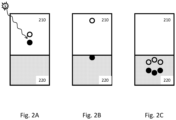
- Fig. 2A, Fig. 2B and Fig. 2C schematically show the operation of an APD, according to an embodiment.
- Fig. 2A shows that when a radiation particle (e.g., an X-ray photon) is absorbed by an absorption region 210, one or more (100 to 10000 for an X-ray photon) electron-hole pairs maybe generated.
- the absorption region 210 has a sufficient thickness and thus a sufficient absorptance (e.g., >80% or >90%) for the incident photon.
- the absorption region 210 may be a silicon layer with a thickness of 10 microns or above.
- the electric field in the absorption region 210 is not high enough to cause avalanche effect in the absorption region 210.
- Fig. 2B shows that the electrons and hole drift in opposite directions in the absorption region 210.
- Fig. 2C shows that avalanche effect occurs in an amplification region 220 when the electrons (or the holes) enter that amplification region 220, thereby generating more electrons and holes.
- the electric field in the amplification region 220 is high enough to cause an avalanche of charge carriers entering the amplification region 220 but not too high to make the avalanche effect self-sustaining.
- a self-sustaining avalanche is an avalanche that persists after the external triggers disappear, such as radiation particles incident on the APD or charge carriers drifted into the APD.
- the electric field in the amplification region 220 may be a result of a doping profile in the amplification region 220, or the structure of the amplification region 220.
- the amplification region 220 may include a p-n junction or a heterojunction that has an electric field in its depletion zone.
- the threshold electric field for the avalanche effect i.e., the electric field above which the avalanche effect occurs and below which the avalanche effect does not occur
- the amplification region 220 may be on one or two opposite sides of the absorption region 210.
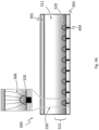
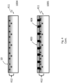
- Fig. 3A schematically shows a cross-sectional view of an apparatus 300 suitable for radiation detection, according to an embodiment.
- the apparatus 300 may comprise a radiation absorption layer 311 and one or more electrodes 304 on the radiation absorption layer 311.
- the radiation absorption layer 311 may be configured to generate charge carriers therein from a radiation particle absorbed by the radiation absorption layer 311.
- the one or more electrodes 304 may be configured to generate an electric field 306 in the radiation absorption layer 311.
- Each of the one or more electrodes 304 may have a geometry (e.g., a small tapered tip) shaping the electric field 306 so that the electric field 306 in one or more portions (i.e., one or more amplification regions 320) of the radiation absorption layer 311 has a field strength sufficient to cause an avalanche of the charge carriers (e.g., electrons or holes) in the one or more amplification regions 320.
- The_charger carriers either generated by the avalanche or directly from the radiation particles, drift to and are collected by the one or more electrodes 304 or a different electrode.
- the apparatus 300 may further include a passivation material 303 configured to passivate a surface of the radiation absorption layer 311 to reduce recombination of charge carriers at the surface.
- the apparatus 300 may_further comprise a counter electrode 301 on the radiation absorption layer 311, the counter electrode 301 being opposite the one or more electrodes 304.
- the counter electrode 301 may be configured to collect charge carriers in the radiation absorption layer 311.
- the radiation absorption layer 311 may comprise a semiconductor material such as silicon.
- the radiation absorption layer 311 may have a sufficient thickness and thus a sufficient absorbance (e.g., >80% or >90%) for incident radiation particles of interest (e.g., X-ray photons).
- the radiation absorption layer 311 may have a thickness of 10 microns or above.
- the radiation absorption layer 311 may be an intrinsic semiconductor.
- the radiation absorption layer 311 may comprise a doped region 312 that is lightly doped with a dopant.
- a semiconductor is considered to be lightly doped when the semiconductor contains a proportion of dopant to semiconductor atom being small enough so that the electronic states of the dopants at the Fermi level are localized (i.e., the band of the dopant may not overlap with the conduction or valence band of the semiconductor).
- lightly doped silicon may have a ratio of dopants to silicon atoms on the order of 1/10 11 .
- the doped region 312 may extend a few microns from a surface into the interior region of the radiation absorption layer 311, and may have a non-zero concentration gradient of the dopant. In the example of Fig. 3A-Fig. 3C , the concentration of the dopant gradually decreases from the surface to the interior region of the radiation absorption layer 311.
- the doped region 312 may be in electrical contact with the electrodes 304. In an embodiment, the doped region 312 may comprise discrete regions, each of which is around one of the electrodes 304.
- the one or more electrodes 304 may comprise a conducting material such as a metal (e.g., gold, copper, aluminum, platinum, etc.), or any other suitable conducting materials (e.g., a heavily doped semiconductor).
- the one or more electrodes 304 may have small dimensions or a suitable shape so that the electric field 306 near the one or more electrodes 304 is concentrated.
- the one or more electrodes 304 may comprise a tip with a shape of cone, frustum, prism, pyramid, cuboid, or cylinder, etc. In the example of Fig. 3A , the tip is flat and cylindrical. The flat tips of the electrodes 304 in Fig.
- the electrical field 306 is not strong enough to cause self-sustaining avalanche; namely, the electric field 306 in the amplification regions 320 should cause avalanche when there are incident radiation particles in the radiation absorption layer 311 but the avalanche should cease without further incident radiation particles in the radiation absorption layer 311.
- a particle of the radiation may generate 10 to 100000 charge carriers.
- One type (electrons or holes) of the charge carriers drift toward the amplification regions 320.
- the charge carriers may drift in directions such that substantially all (more than 98%, more than 99.5%, more than 99.9% or more than 99.99% of) charge carriers generated by a radiation particle incident around the footprint 330 of one of the electrodes 304 flow to the amplification region 320 corresponding to the electrode 304. Namely, less than 2%, less than 0.5%, less than 0.1%, or less than 0.01% of these charge carriers flow beyond the amplification region 320 corresponding to the electrode 304.
- the avalanche effect occurs and causes amplification of the charge carriers.
- the amplified charge carriers can be collected through the corresponding electrodes 304, as an electric current.
- the electric current is proportional to the number of incident radiation particles around the footprint 330 of the electrode 304 per unit time (i.e., proportional to the radiation intensity).
- the electric currents at the electrodes 304 may be compiled to represent a spatial intensity distribution of radiation, i.e., an image.
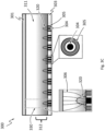
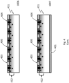
- Fig. 3B shows a variant of the apparatus 300, where the electrodes 304 may extended into the radiation absorption layer 311, according to an embodiment.
- the portion of each of the electrodes 304 extending into radiation absorption layer 311 may have small dimensions or a suitable shape so that the electric field 306 near the portion is concentrated.
- the portion may comprise a tip with a shape of cone, frustum, prism, pyramid, cuboid, or cylinder, etc.
- the tip is tapered, and the electric field 306 near the tapered tips become strong enough to cause avalanche of charge carriers near the tips.
- the strength of the electrical field 306 increases when approaching the portions of the electrodes 304, and the amplification regions 320 in Fig. 3B are regions around the portions where the electrical field 306 is strong enough to cause avalanche of charge carriers.
- Fig. 3C shows a variant of the apparatus 300, where the apparatus 300 may further comprise one or more outer electrodes 305, according to an embodiment.
- the one or more outer electrodes 305 correspond to and locate around the one or more electrodes 304 respectively.
- the outer electrodes 305 are electrically insulated from the electrodes 304.
- an insulation region e.g., a portion of the passivation material 303 may exist in between an outer electrode 305 and its corresponding electrode 304.
- a semiconductor substrate 411 is obtained.
- the semiconductor substrate 411 may comprise an intrinsic semiconductor such as silicon.
- the semiconductor substrate 411 may have a sufficient thickness and thus a sufficient absorbance (e.g., >80% or >90%) for incident radiation particles of interest (e.g., X-ray photons).
- the semiconductor substrate 411 may have a thickness of 10 microns or above.
- the semiconductor substrate 411 may be doped to form a doped region 412 (shown in step 1004-step 1006).
- the doped region 412 may function as the doped region 312 of the radiation absorption layer 311 in Fig. 3A- Fig. 3C .
- the doped region 412 to be formed is a continuous layer.
- the semiconductor substrate 411 is a silicon substrate, the desired doped region 412 is lightly doped and have a non-zero concentration gradient of the dopant extending a few microns from the surface into the interior region of the semiconductor substrate 411. The concentration of the dopant may gradually decrease from the surface to the interior region of the semiconductor substrate 411.
- a mask layer 402 is formed on a surface of the semiconductor substrate 411.
- the mask layer 402 may serve as a screening layer configured to retard entry of dopants into the semiconductor substrate 411 in the step 1002 of doping.
- the mask layer 402 may comprise a material such as silicon dioxide.
- the thickness of the mask layer 402 may be determined according to doping conditions in step 1002 and desired doping profile of the doped region 412 (shown in step 1004-step 1006) to be formed.
- the mask layer 402 may be formed onto the surface by various techniques, such as thermal oxidation, vapor deposition, spin coating, sputtering or any other suitable processes.
- a surface of the semiconductor substrate 411 is light doped with a suitable dopant 10 by a doping technique such as dopant diffusion and ion implantation.
- the rate of dopant entering into the semiconductor substrate 411 may be controlled by the mask layer 402, the dose of dopants doped, and doping details such as the energy of the dopants during an ion implantation.
- the mask layer 402 may be removed by wet etching, chemical mechanical polishing or some other suitable techniques.
- the etching process may be carried out by a technique such as dry etching (e.g., deep reactive-ion etching), wet etching (e.g., anisotropic wet etching), or a combination thereof.
- Conducing materials such as metal (e.g., gold, copper, aluminum, platinum, etc.) may be deposited into the recesses to form the electrodes 404 by a suitable technique such as physical vapor deposition, chemical vapor deposition, spin coating, sputtering, etc.
- the mask may be kept and server as a passivation layer of the surface of the substrate 411. In an embodiment, the mask may be removed and a passivation material 403 may be applied to passivate the surface of the substrate 411.
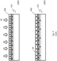
- outer electrodes 405 may be formed around the electrodes 404.
- the electrodes 405 may function as the outer electrodes 305 in Fig. 3C .
- Forming the outer electrodes 405 may involve mask forming and metal deposition processes similar to the step 1005.
- a counter electrode 401 may be formed on another surface of the semiconductor substrate 411.
- the counter electrode 401 may function as the counter electrode 301 of the apparatus 300.
- the counter electrode 401 is planar and may be formed by depositing conducting materials such as metals onto the other surface of the semiconductor substrate 411 by a suitable technique such as vapor deposition, sputtering, etc.
- Forming the apparatus 300 may comprise some intermediate steps such as surface cleaning, polishing, surface passivation, which are not shown in Fig. 4 .
- the order of the steps shown in Fig. 4 may be changed to suit different formation needs.
- Fig. 5 schematically shows a system comprising an imaging sensor 503 being an embodiment of the apparatus 300 described herein.
- the system comprises an X-ray source 501.
- X-ray emitted from the X-ray source 501 penetrates an object 510 (e.g., diamonds, tissue samples, a human body part such as breast), is attenuated by different degrees by the internal structures of the object 510, and is projected to the image sensor 503.
- the image sensor 503 forms an image by detecting the intensity distribution of the X-ray.
- the system may be used for medical imaging such as chest X-ray radiography, abdominal X-ray radiography, dental X-ray radiography, mammography, etc.
- the system may be used for industrial CT, such as diamond defect detection, scanning a tree to visualize year periodicity and cell structure, scanning building material like concrete after loading, etc.
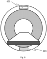
- Fig. 6 schematically shows an X-ray computed tomography (X-ray CT) system.
- the X-ray CT system uses computer-processed X-rays to produce tomographic images (virtual "slices") of specific areas of a scanned object.
- the tomographic images may be used for diagnostic and therapeutic purposes in various medical disciplines, or for flaw detection, failure analysis, metrology, assembly analysis and reverse engineering.
- the X-ray CT system comprises the image sensor 603 being an embodiment of the apparatus 300 described herein and an X-ray source 601.
- the image sensor 603 and the X-ray source 601 may be configured to rotate synchronously along one or more circular or spiral paths.
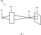
- Fig. 7 schematically shows an X-ray microscope or X-ray micro CT 700.
- the X-ray microscope or X-ray micro CT 700 may include an X-ray source 701, focusing optics 704, and the image sensor 703 being an embodiment of the apparatus 300 described herein, for detecting an X-ray image of a sample 702.
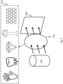
- Fig. 8 schematically shows a system 800 suitable for laser scanning, according to an embodiment.
- the system 800 comprises a laser source 810 and a detector 820 being an embodiment of the apparatus 300 described herein.
- the laser source 810 may be configured to generate a scanning laser beam.
- the scanning laser beam may be infrared.
- the laser source 810 may perform two-dimensional laser scanning without moving part.
- the detector 820 may be configured to collect return laser signals after the scanning laser beam bounces off an object, building or landscape and generate electrical signals.
- the system 800 may further comprise a signal processing system configured to process and analyze the electrical signals generated by the detector 820. In one embodiment, the distance and shape of the object, building or landscape may be obtained.
- the system 800 may be a Lidar system (e.g., an on-vehicle Lidar).
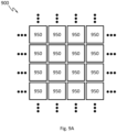
- Fig. 9A schematically shows a radiation detector 900, as an example.
- the radiation detector 900 has an array of pixels 950.
- the array may be a rectangular array, a honeycomb array, a hexagonal array or any other suitable array.
- Each pixel 950 is configured to detect radiation from a radiation source incident thereon and may be configured measure a characteristic (e.g., the energy of the particles, the intensity distribution) of the radiation.
- Each pixel 950 may have its own analog-to-digital converter (ADC) configured to digitize an analog signal representing the energy of an incident radiation particle into a digital signal, or to digitize an analog signal representing the total energy of a plurality of incident radiation particles into a digital signal.
- ADC analog-to-digital converter
- the pixels 950 may be configured to operate in parallel. For example, when one pixel 950 measures an incident radiation particle, another pixel 950 may be waiting for a radiation particle to arrive.
- the pixels 950 may not have to be individually addressable.
- the electronics layer 920 may include an electronic system 921 suitable for processing or interpreting the electrical signals.
- the electronic system 921 may include an analog circuitry such as a filter network, amplifiers, integrators, and comparators, or a digital circuitry such as a microprocessors, and memory.
- the electronic system 921 may include one or more ADCs.
- the electronic system 921 may include components shared by the pixels or components dedicated to a single pixel.
- the electronic system 921 may include an amplifier dedicated to each pixel and a microprocessor shared among all the pixels.
- the electronic system 921 may be electrically connected to the pixels by vias 931. Space among the vias may be filled with a filler material 930, which may increase the mechanical stability of the connection of the electronics layer 920 to the radiation absorption layer 910. Other bonding techniques are possible to connect the electronic system 921 to the pixels without using vias.
- Fig. 10A and Fig. 10B each show a component diagram of the electronic system 921, according to an embodiment.
- the electronic system 921 may include a first voltage comparator 1901, a second voltage comparator 1902, a counter 1920, a switch 1905, a voltmeter 1906 and a controller 1910.
- the first voltage comparator 1901 is configured to compare the voltage of an electrode (e.g., one of the electrodes 904 in Fig. 9B ) to a first threshold.
- the first voltage comparator 1901 may be configured to monitor the voltage directly, or calculate the voltage by integrating an electric current flowing through the electrode over a period of time.
- the first voltage comparator 1901 may be controllably activated or deactivated by the controller 1910.
- the first voltage comparator 1901 may be a continuous comparator. Namely, the first voltage comparator 1901 may be configured to be activated continuously, and monitor the voltage continuously.
- the first voltage comparator 1901 configured as a continuous comparator reduces the chance that the system 921 misses signals generated directly by an incident radiation particle or by charge carrier avalanche.
- the first voltage comparator 1901 configured as a continuous comparator is especially suitable when the incident radiation intensity is relatively high.
- the first voltage comparator 1901 may be a clocked comparator, which has the benefit of lower power consumption.
- the first voltage comparator 1901 configured as a clocked comparator may cause the system 921 to miss signals generated directly by some incident radiation particles or by charge carrier avalanche. When the incident radiation intensity is low, the chance of missing an incident radiation particle is low because the time interval between two successive radiation particles is relatively long. Therefore, the first voltage comparator 1901 configured as a clocked comparator is especially suitable when the incident radiation intensity is relatively low.
- the first threshold may be 5-10%, 10%-20%, 20-30%, 30-40% or 40-50% of the maximum voltage one incident radiation particle may generate directly in the radiation absorption layer or after being amplified by avalanche in the radiation absorption layer.
- the maximum voltage may depend on the energy of the incident radiation particle (i.e., the wavelength of the incident radiation), the material of the radiation absorption layer 910, magnitude of charge carrier avalanche and other factors.
- the first threshold may be 50 mV, 100 mV, 150 mV, or 200 mV.
- the second voltage comparator 1902 is configured to compare the voltage to a second threshold.
- the second voltage comparator 1902 may be configured to monitor the voltage directly, or calculate the voltage by integrating an electric current flowing through the electrode over a period of time.
- the second voltage comparator 1902 may be a continuous comparator.
- the second voltage comparator 1902 may be controllably activated or deacivated by the controller 1910. When the second voltage comparator 1902 is deactivated, the power consumption of the second voltage comparator 1902 may be less than 1%, less than 5%, less than 10% or less than 20% of the power consumption when the second voltage comparator 1902 is activated.
- the absolute value of the second threshold is greater than the absolute value of the first threshold.
- the first voltage comparator 1901 or the second voltage comparator 1902 may include one or more op-amps or any other suitable circuitry.
- the first voltage comparator 1901 or the second voltage comparator 1902 may have a high speed to allow the system 921 to operate under a high flux of incident radiation particle. However, having a high speed is often at the cost of power consumption.
- the counter 1920 is configured to register a number of radiation particles reaching the radiation absorption layer.
- the counter 1920 may be a software component (e.g., a number stored in a computer memory) or a hardware component (e.g., a 4017 IC and a 7490 IC).
- the controller 1910 may be configured to cause the voltmeter 1906 to measure the voltage upon expiration of the time delay.
- the controller 1910 may be configured to connect the electrode to an electrical ground, so as to reset the voltage and discharge any charge carriers accumulated on the electrode.
- the electrode is connected to an electrical ground after the expiration of the time delay.
- the electrode is connected to an electrical ground for a finite reset time period.
- the controller 1910 may connect the electrode to the electrical ground by controlling the switch 1905.
- the switch 1905 may be a transistor such as a field-effect transistor (FET).
- the system 921 has no analog filter network (e.g., a RC network). In an embodiment, the system 921 has no analog circuitry.
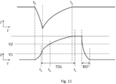
- Fig. 11 schematically shows a temporal change of the electric current flowing through the electrode (upper curve) caused by charge carriers generated by an incident radiation particle or charge carrier avalanche in the radiation absorption layer, and a corresponding temporal change of the voltage of the electrode (lower curve).
- the voltage may be an integral of the electric current with respect to time.
- the radiation particle hits the radiation absorption layer, charge carriers start being generated and being amplified in the radiation absorption layer, electric current starts to flow through the electrode, and the absolute value of the voltage of the electrode starts to increase.
- the first voltage comparator 1901 determines that the absolute value of the voltage equals or exceeds the absolute value of the first threshold V1, and the controller 1910 starts the time delay TD1 and the controller 1910 may deactivate the first voltage comparator 1901 at the beginning of TD1. If the controller 1910 is deactivated before t 1 , the controller 1910 is activated at t 1 . During TD1, the controller 1910 activates the second voltage comparator 1902. The term "during" a time delay as used here means the beginning and the expiration (i.e., the end) and any time in between. For example, the controller 1910 may activate the second voltage comparator 1902 at the expiration of TD1.
- the controller 1910 causes the number registered by the counter 1920 to increase by one.
- time t e all charge carriers generated by the radiation particle drift out of the radiation absorption layer 910.
- time t s the time delay TD1 expires.
- time t s is after time t e ; namely TD1 expires after all charge carriers generated by the radiation particle or charge carrier avalanche drift out of the radiation absorption layer 910.
- the rate of change of the voltage is thus substantially zero at t s .
- the controller 1910 may be configured to deactivate the second voltage comparator 1902 at expiration of TD1 or at t 2 , or any time in between.
- the controller 1910 may be configured to cause the voltmeter 1906 to measure the voltage upon expiration of the time delay TD1. In an embodiment, the controller 1910 causes the voltmeter 1906 to measure the voltage after the rate of change of the voltage becomes substantially zero after the expiration of the time delay TD1. The voltage at this moment is proportional to the amount of charge carriers generated by a radiation particle or amplified by the avalanche, which relates to the energy of the radiation particle.
- the controller 1910 may be configured to determine the energy of the radiation particle based on voltage the voltmeter 1906 measures. One way to determine the energy is by binning the voltage.
- the counter 1920 may have a sub-counter for each bin.
Landscapes
- Health & Medical Sciences (AREA)
- Life Sciences & Earth Sciences (AREA)
- Engineering & Computer Science (AREA)
- Physics & Mathematics (AREA)
- High Energy & Nuclear Physics (AREA)
- Molecular Biology (AREA)
- Medical Informatics (AREA)
- Dentistry (AREA)
- Oral & Maxillofacial Surgery (AREA)
- Nuclear Medicine, Radiotherapy & Molecular Imaging (AREA)
- Surgery (AREA)
- Spectroscopy & Molecular Physics (AREA)
- General Physics & Mathematics (AREA)
- Optics & Photonics (AREA)
- Pathology (AREA)
- Radiology & Medical Imaging (AREA)
- Biomedical Technology (AREA)
- Heart & Thoracic Surgery (AREA)
- Biophysics (AREA)
- Animal Behavior & Ethology (AREA)
- General Health & Medical Sciences (AREA)
- Public Health (AREA)
- Veterinary Medicine (AREA)
- Microelectronics & Electronic Packaging (AREA)
- Measurement Of Radiation (AREA)
- Analysing Materials By The Use Of Radiation (AREA)
- Nuclear Medicine (AREA)
Claims (14)
- Vorrichtung (300), umfassend:Strahlungsabsorptionsschicht (311), die konfiguriert ist, darin Ladungsträger aus einem Strahlungsteilchen, das von der Strahlungsabsorptionsschicht absorbiert ist, zu erzeugen, die Strahlungsabsorptionsschicht umfasst dabei ein Halbleitermaterial mit einer dotierten Region (312);eine erste Elektrode (304) auf einer Oberfläche der Strahlungsabsorptionsschicht in elektrischem Kontakt mit der dotierten Region;eine zweite Elektrode (301)wobei die erste Elektrode eine Spitze umfasst, die kegelförmig ist oder die Form eines Konus, Kegelstumpfs, Prismas, einer Pyramide, eines Quaders oder Zylinders hat, um eine Geometrie zu definieren, die konfiguriert ist, ein elektrisches Feld zwischen der ersten und zweiten Elektrode in einer Verstärkungsregion der Strahlungsabsorptionsschicht zu erzeugen, wobei das elektrische Feld eine Feldstärke hat, die ausreicht, um eine Lawinenbildung des Ladungsträgers in der Verstärkungsregion zu verursachen;die Vorrichtung ist dadurch gekennzeichnet, dass die zweite Elektrode (301) auf einer gegenüberliegenden Oberfläche der Strahlungsabsorptionsschicht von der ersten Elektrode (304) liegt.
- Vorrichtung nach Anspruch 1, wobei die zweite Elektrode konfiguriert ist, die Ladungsträger in der Strahlungsabsorptionsschicht zu sammeln; wobei die erste Elektrode konfiguriert ist, die Ladungsträger, die direkt von dem Strahlungsteilchen oder durch die Lawinenbildung erzeugt werden, zu sammeln.
- Vorrichtung nach Anspruch 1, wobei die zweite Elektrode abgegrenzte Regionen umfasst; wobei sich die abgegrenzten Regionen der zweiten Elektrode in die Strahlungsabsorptionsschicht erstrecken.
- Vorrichtung nach Anspruch 1, wobei die erste Elektrode konfiguriert ist, das elektrische Feld zu konzentrieren; wobei sich die erste Elektrode in die Strahlungsabsorptionsschicht erstreckt.
- Vorrichtung nach Anspruch 1, ferner umfassend eine Außenelektrode, die um die erste Elektrode angeordnet und von der ersten Elektrode elektrisch isoliert ist; wobei die Außenelektrode konfiguriert ist, das elektrische Feld in der Verstärkungsregion zu formen.
- Vorrichtung nach Anspruch 5, wobei die Außenelektrode so konfiguriert ist, dass sie keine Ladungsträger sammelt.
- Vorrichtung nach Anspruch 1, wobei die Verstärkungsregion die dotierte Region des Halbleitermaterials in elektrischem Kontakt mit der ersten Elektrode umfasst.
- Vorrichtung nach Anspruch 7, wobei der dotierte Halbleiter einen von Null verschiedenen Konzentrationsgradienten eines Dopanden aufweist.
- Verfahren umfassend:Bilden (1002) einer dotierten Region (312) eines Halbleitersubstrats durch Dotieren einer Oberfläche des Halbleitersubstrats mit Dopanden;Einbringen (1003) der Dopanden in das Halbleitersubstrat durch Tempern des Halbleitersubstrats;Kontrollieren eines Dotierungsprofils der dotierten Region durch Wiederholen des Dotierens und Temperns des Halbleitersubstrats;Bilden (1005) einer ersten Elektrode (304) auf einer Oberfläche eines Halbleitersubstrats, wobei die erste Elektrode in elektrischem Kontakt mit der dotierten Region ist und eine Spitze umfasst, die kegelförmig ist oder die Form eines Konus, Kegelstumpfs, Prismas, einer Pyramide, eines Quaders oder Zylinders hat;Bilden (1005) einer zweiten Elektrode (301) auf einer gegenüberliegenden Oberfläche der Strahlungsabsorptionsschicht von der ersten Elektrode; undBilden (1006) einer Außenelektrode (305), die um die erste Elektrode angeordnet ist, wobei die Außenelektrode von der ersten Elektrode elektrisch isoliert ist.
- Verfahren nach Anspruch 9, wobei die dotierte Region einen von Null verschiedenen Konzentrationsgradienten eines Dopanden aufweist.
- Verfahren nach Anspruch 9, ferner umfassend das Bilden einer Abschirmschicht auf der Oberfläche des Halbleitersubstrats vor dem Dotieren des Halbleitersubstrats, wobei die Abschirmschicht konfiguriert ist, das Eintreten von Dopanden in das Halbleitersubstrat zu verzögern.
- Verfahren nach Anspruch 9, wobei sich die erste Elektrode in das Halbleitersubstrat erstreckt.
- Verfahren nach Anspruch 9, wobei die Außenelektrode abgegrenzte Regionen umfasst.
- Verfahren nach Anspruch 9, wobei die zweite Elektrode abgegrenzte Regionen umfasst; wobei sich die abgegrenzten Regionen der zweiten Elektrode in die Strahlungsabsorptionsschicht erstrecken.
Applications Claiming Priority (1)
| Application Number | Priority Date | Filing Date | Title |
|---|---|---|---|
| PCT/CN2017/108240 WO2019084701A1 (en) | 2017-10-30 | 2017-10-30 | Image sensor based on charge carrier avalanche |
Publications (3)
| Publication Number | Publication Date |
|---|---|
| EP3704517A1 EP3704517A1 (de) | 2020-09-09 |
| EP3704517A4 EP3704517A4 (de) | 2021-06-23 |
| EP3704517B1 true EP3704517B1 (de) | 2025-07-02 |
Family
ID=66331264
Family Applications (1)
| Application Number | Title | Priority Date | Filing Date |
|---|---|---|---|
| EP17930608.9A Active EP3704517B1 (de) | 2017-10-30 | 2017-10-30 | Bildsensor auf der basis einer ladungsträgerlawine |
Country Status (5)
| Country | Link |
|---|---|
| US (3) | US11187819B2 (de) |
| EP (1) | EP3704517B1 (de) |
| CN (1) | CN111247455B (de) |
| TW (1) | TWI810215B (de) |
| WO (1) | WO2019084701A1 (de) |
Families Citing this family (7)
| Publication number | Priority date | Publication date | Assignee | Title |
|---|---|---|---|---|
| EP3821473B1 (de) * | 2018-07-12 | 2023-07-05 | Shenzhen Xpectvision Technology Co., Ltd. | Bildsensoren mit silbernanopartikelelektroden |
| CN114096885A (zh) * | 2019-07-30 | 2022-02-25 | 深圳源光科技有限公司 | 用于电话机的激光雷达系统 |
| EP4111180A1 (de) * | 2020-02-27 | 2023-01-04 | Shenzhen Xpectvision Technology Co., Ltd. | Verfahren zur phasenkontrastbildgebung |
| CN115023605A (zh) * | 2020-02-27 | 2022-09-06 | 深圳帧观德芯科技有限公司 | 相位对比成像法 |
| CN116171393B (zh) * | 2020-11-30 | 2025-12-12 | 苏州帧观传感科技有限公司 | 一种基于电荷载流子雪崩的图像传感器 |
| CN118215255A (zh) * | 2022-01-27 | 2024-06-18 | 武汉领普科技有限公司 | 位姿变换装置以及人体传感器及其处理方法、控制系统 |
| WO2024152288A1 (en) * | 2023-01-19 | 2024-07-25 | Shenzhen Xpectvision Technology Co., Ltd. | Semiconductor radiation detector |
Citations (1)
| Publication number | Priority date | Publication date | Assignee | Title |
|---|---|---|---|---|
| US20120326012A1 (en) * | 2009-07-31 | 2012-12-27 | International Business Machines Corporation | Avalanche impact ionization amplification devices |
Family Cites Families (15)
| Publication number | Priority date | Publication date | Assignee | Title |
|---|---|---|---|---|
| JPS6215864A (ja) * | 1985-07-15 | 1987-01-24 | Hitachi Ltd | 太陽電池の製造方法 |
| US6046454A (en) * | 1995-10-13 | 2000-04-04 | Digirad Corporation | Semiconductor radiation detector with enhanced charge collection |
| US5844291A (en) * | 1996-12-20 | 1998-12-01 | Board Of Regents, The University Of Texas System | Wide wavelength range high efficiency avalanche light detector with negative feedback |
| US6204087B1 (en) * | 1997-02-07 | 2001-03-20 | University Of Hawai'i | Fabrication of three-dimensional architecture for solid state radiation detectors |
| SE530172C2 (sv) * | 2000-03-31 | 2008-03-18 | Xcounter Ab | Spektralt upplöst detektering av joniserande strålning |
| US7138291B2 (en) * | 2003-01-30 | 2006-11-21 | Cree, Inc. | Methods of treating a silicon carbide substrate for improved epitaxial deposition and resulting structures and devices |
| US6885827B2 (en) * | 2002-07-30 | 2005-04-26 | Amplification Technologies, Inc. | High sensitivity, high resolution detection of signals |
| CN100514680C (zh) * | 2007-04-04 | 2009-07-15 | 厦门大学 | 一种δ掺杂4H-SiC雪崩紫外光电探测器及其制备方法 |
| JP5108369B2 (ja) * | 2007-05-07 | 2012-12-26 | 富士フイルム株式会社 | 撮像素子の製造方法及び撮像素子の駆動方法 |
| EP2443656B1 (de) * | 2009-06-17 | 2018-11-07 | The Regents of the University of Michigan | Photodiode und andere sensorstrukturen in flachen röntgenbildgebern sowie verfahren zur verbesserung der topologischen gleichförmigkeit der photodiode und der anderen strukturen in dem flachen röntgenbildgeber auf dünnschichtelektronikbasis |
| JP5602598B2 (ja) * | 2010-11-29 | 2014-10-08 | 富士フイルム株式会社 | 放射線検出器及び放射線検出器の製造方法 |
| CN102237416A (zh) * | 2011-07-05 | 2011-11-09 | 江苏能华微电子科技发展有限公司 | 一种用于紫外探测的雪崩光电二极管及其制备方法和工作方法 |
| US9006063B2 (en) * | 2013-06-28 | 2015-04-14 | Stmicroelectronics S.R.L. | Trench MOSFET |
| CN107710021B (zh) * | 2015-07-09 | 2019-09-27 | 深圳帧观德芯科技有限公司 | 制作半导体x射线检测器的方法 |
| US10074685B1 (en) * | 2017-05-17 | 2018-09-11 | Prismatic Sensors Ab | X-ray sensor, x-ray detector system and x-ray imaging system |
-
2017
- 2017-10-30 EP EP17930608.9A patent/EP3704517B1/de active Active
- 2017-10-30 WO PCT/CN2017/108240 patent/WO2019084701A1/en not_active Ceased
- 2017-10-30 CN CN201780096003.1A patent/CN111247455B/zh active Active
-
2018
- 2018-10-29 TW TW107138217A patent/TWI810215B/zh active
-
2020
- 2020-04-21 US US16/854,035 patent/US11187819B2/en not_active Expired - Fee Related
-
2021
- 2021-10-29 US US17/514,154 patent/US11619754B2/en active Active
-
2023
- 2023-03-02 US US18/116,547 patent/US20230204804A1/en not_active Abandoned
Patent Citations (1)
| Publication number | Priority date | Publication date | Assignee | Title |
|---|---|---|---|---|
| US20120326012A1 (en) * | 2009-07-31 | 2012-12-27 | International Business Machines Corporation | Avalanche impact ionization amplification devices |
Also Published As
| Publication number | Publication date |
|---|---|
| TWI810215B (zh) | 2023-08-01 |
| CN111247455B (zh) | 2023-11-10 |
| US11187819B2 (en) | 2021-11-30 |
| EP3704517A1 (de) | 2020-09-09 |
| US20200249367A1 (en) | 2020-08-06 |
| EP3704517A4 (de) | 2021-06-23 |
| TW201917419A (zh) | 2019-05-01 |
| US11619754B2 (en) | 2023-04-04 |
| CN111247455A (zh) | 2020-06-05 |
| WO2019084701A1 (en) | 2019-05-09 |
| US20220050219A1 (en) | 2022-02-17 |
| US20230204804A1 (en) | 2023-06-29 |
Similar Documents
| Publication | Publication Date | Title |
|---|---|---|
| US11619754B2 (en) | Image sensor based on charge carrier avalanche | |
| US11114494B2 (en) | Image sensor based on avalanche photodiodes | |
| US11860322B2 (en) | Radiation detector capable of noise handling | |
| US20210169430A1 (en) | Apparatus and method for imaging an object using radiation | |
| US20230307472A1 (en) | Image sensor based on charge carrier avalanche | |
| US11114578B2 (en) | Image sensors with silver-nanoparticle electrodes | |
| CN110914714B (zh) | 制造和使用x射线检测器的方法 | |
| CN116457663B (zh) | 使用x射线荧光进行生物分析物研究的装置和方法 | |
| CN112912768B (zh) | 使用x射线荧光成像的方法 | |
| Audet et al. | High-purity silicon sensor array for imaging soft X-ray and infrared radiation |
Legal Events
| Date | Code | Title | Description |
|---|---|---|---|
| STAA | Information on the status of an ep patent application or granted ep patent |
Free format text: STATUS: THE INTERNATIONAL PUBLICATION HAS BEEN MADE |
|
| PUAI | Public reference made under article 153(3) epc to a published international application that has entered the european phase |
Free format text: ORIGINAL CODE: 0009012 |
|
| STAA | Information on the status of an ep patent application or granted ep patent |
Free format text: STATUS: REQUEST FOR EXAMINATION WAS MADE |
|
| 17P | Request for examination filed |
Effective date: 20200522 |
|
| AK | Designated contracting states |
Kind code of ref document: A1 Designated state(s): AL AT BE BG CH CY CZ DE DK EE ES FI FR GB GR HR HU IE IS IT LI LT LU LV MC MK MT NL NO PL PT RO RS SE SI SK SM TR |
|
| AX | Request for extension of the european patent |
Extension state: BA ME |
|
| DAV | Request for validation of the european patent (deleted) | ||
| DAX | Request for extension of the european patent (deleted) | ||
| A4 | Supplementary search report drawn up and despatched |
Effective date: 20210521 |
|
| RIC1 | Information provided on ipc code assigned before grant |
Ipc: G01T 1/36 20060101AFI20210517BHEP Ipc: G01T 1/24 20060101ALI20210517BHEP |
|
| RAP3 | Party data changed (applicant data changed or rights of an application transferred) |
Owner name: SHENZHEN XPECTVISION TECHNOLOGY CO., LTD. |
|
| STAA | Information on the status of an ep patent application or granted ep patent |
Free format text: STATUS: EXAMINATION IS IN PROGRESS |
|
| 17Q | First examination report despatched |
Effective date: 20230206 |
|
| P01 | Opt-out of the competence of the unified patent court (upc) registered |
Effective date: 20230522 |
|
| GRAP | Despatch of communication of intention to grant a patent |
Free format text: ORIGINAL CODE: EPIDOSNIGR1 |
|
| STAA | Information on the status of an ep patent application or granted ep patent |
Free format text: STATUS: GRANT OF PATENT IS INTENDED |
|
| INTG | Intention to grant announced |
Effective date: 20250411 |
|
| GRAS | Grant fee paid |
Free format text: ORIGINAL CODE: EPIDOSNIGR3 |
|
| GRAA | (expected) grant |
Free format text: ORIGINAL CODE: 0009210 |
|
| STAA | Information on the status of an ep patent application or granted ep patent |
Free format text: STATUS: THE PATENT HAS BEEN GRANTED |
|
| AK | Designated contracting states |
Kind code of ref document: B1 Designated state(s): AL AT BE BG CH CY CZ DE DK EE ES FI FR GB GR HR HU IE IS IT LI LT LU LV MC MK MT NL NO PL PT RO RS SE SI SK SM TR |
|
| REG | Reference to a national code |
Ref country code: GB Ref legal event code: FG4D |
|
| RIN1 | Information on inventor provided before grant (corrected) |
Inventor name: LIU, YURUN Inventor name: CAO, PEIYAN |
|
| REG | Reference to a national code |
Ref country code: CH Ref legal event code: EP |
|
| REG | Reference to a national code |
Ref country code: DE Ref legal event code: R096 Ref document number: 602017090370 Country of ref document: DE |
|
| REG | Reference to a national code |
Ref country code: IE Ref legal event code: FG4D |
|
| REG | Reference to a national code |
Ref country code: NL Ref legal event code: MP Effective date: 20250702 |
|
| PG25 | Lapsed in a contracting state [announced via postgrant information from national office to epo] |
Ref country code: PT Free format text: LAPSE BECAUSE OF FAILURE TO SUBMIT A TRANSLATION OF THE DESCRIPTION OR TO PAY THE FEE WITHIN THE PRESCRIBED TIME-LIMIT Effective date: 20251103 |
|
| PG25 | Lapsed in a contracting state [announced via postgrant information from national office to epo] |
Ref country code: NL Free format text: LAPSE BECAUSE OF FAILURE TO SUBMIT A TRANSLATION OF THE DESCRIPTION OR TO PAY THE FEE WITHIN THE PRESCRIBED TIME-LIMIT Effective date: 20250702 |
|
| REG | Reference to a national code |
Ref country code: AT Ref legal event code: MK05 Ref document number: 1809846 Country of ref document: AT Kind code of ref document: T Effective date: 20250702 |
|
| PG25 | Lapsed in a contracting state [announced via postgrant information from national office to epo] |
Ref country code: IS Free format text: LAPSE BECAUSE OF FAILURE TO SUBMIT A TRANSLATION OF THE DESCRIPTION OR TO PAY THE FEE WITHIN THE PRESCRIBED TIME-LIMIT Effective date: 20251102 |
|
| PG25 | Lapsed in a contracting state [announced via postgrant information from national office to epo] |
Ref country code: NO Free format text: LAPSE BECAUSE OF FAILURE TO SUBMIT A TRANSLATION OF THE DESCRIPTION OR TO PAY THE FEE WITHIN THE PRESCRIBED TIME-LIMIT Effective date: 20251002 |
|
| REG | Reference to a national code |
Ref country code: LT Ref legal event code: MG9D |
|
| PG25 | Lapsed in a contracting state [announced via postgrant information from national office to epo] |
Ref country code: AT Free format text: LAPSE BECAUSE OF FAILURE TO SUBMIT A TRANSLATION OF THE DESCRIPTION OR TO PAY THE FEE WITHIN THE PRESCRIBED TIME-LIMIT Effective date: 20250702 |
|
| PG25 | Lapsed in a contracting state [announced via postgrant information from national office to epo] |
Ref country code: FI Free format text: LAPSE BECAUSE OF FAILURE TO SUBMIT A TRANSLATION OF THE DESCRIPTION OR TO PAY THE FEE WITHIN THE PRESCRIBED TIME-LIMIT Effective date: 20250702 |
|
| PG25 | Lapsed in a contracting state [announced via postgrant information from national office to epo] |
Ref country code: HR Free format text: LAPSE BECAUSE OF FAILURE TO SUBMIT A TRANSLATION OF THE DESCRIPTION OR TO PAY THE FEE WITHIN THE PRESCRIBED TIME-LIMIT Effective date: 20250702 |
|
| PG25 | Lapsed in a contracting state [announced via postgrant information from national office to epo] |
Ref country code: GR Free format text: LAPSE BECAUSE OF FAILURE TO SUBMIT A TRANSLATION OF THE DESCRIPTION OR TO PAY THE FEE WITHIN THE PRESCRIBED TIME-LIMIT Effective date: 20251003 |
|
| PG25 | Lapsed in a contracting state [announced via postgrant information from national office to epo] |
Ref country code: SE Free format text: LAPSE BECAUSE OF FAILURE TO SUBMIT A TRANSLATION OF THE DESCRIPTION OR TO PAY THE FEE WITHIN THE PRESCRIBED TIME-LIMIT Effective date: 20250702 Ref country code: CZ Free format text: LAPSE BECAUSE OF FAILURE TO SUBMIT A TRANSLATION OF THE DESCRIPTION OR TO PAY THE FEE WITHIN THE PRESCRIBED TIME-LIMIT Effective date: 20250702 |
|
| PG25 | Lapsed in a contracting state [announced via postgrant information from national office to epo] |
Ref country code: LV Free format text: LAPSE BECAUSE OF FAILURE TO SUBMIT A TRANSLATION OF THE DESCRIPTION OR TO PAY THE FEE WITHIN THE PRESCRIBED TIME-LIMIT Effective date: 20250702 |
|
| PG25 | Lapsed in a contracting state [announced via postgrant information from national office to epo] |
Ref country code: BG Free format text: LAPSE BECAUSE OF FAILURE TO SUBMIT A TRANSLATION OF THE DESCRIPTION OR TO PAY THE FEE WITHIN THE PRESCRIBED TIME-LIMIT Effective date: 20250702 Ref country code: PL Free format text: LAPSE BECAUSE OF FAILURE TO SUBMIT A TRANSLATION OF THE DESCRIPTION OR TO PAY THE FEE WITHIN THE PRESCRIBED TIME-LIMIT Effective date: 20250702 |
|
| PG25 | Lapsed in a contracting state [announced via postgrant information from national office to epo] |
Ref country code: RS Free format text: LAPSE BECAUSE OF FAILURE TO SUBMIT A TRANSLATION OF THE DESCRIPTION OR TO PAY THE FEE WITHIN THE PRESCRIBED TIME-LIMIT Effective date: 20251002 |
|
| PG25 | Lapsed in a contracting state [announced via postgrant information from national office to epo] |
Ref country code: ES Free format text: LAPSE BECAUSE OF FAILURE TO SUBMIT A TRANSLATION OF THE DESCRIPTION OR TO PAY THE FEE WITHIN THE PRESCRIBED TIME-LIMIT Effective date: 20250702 |
|
| PG25 | Lapsed in a contracting state [announced via postgrant information from national office to epo] |
Ref country code: RO Free format text: LAPSE BECAUSE OF FAILURE TO SUBMIT A TRANSLATION OF THE DESCRIPTION OR TO PAY THE FEE WITHIN THE PRESCRIBED TIME-LIMIT Effective date: 20250702 |
|
| PG25 | Lapsed in a contracting state [announced via postgrant information from national office to epo] |
Ref country code: SM Free format text: LAPSE BECAUSE OF FAILURE TO SUBMIT A TRANSLATION OF THE DESCRIPTION OR TO PAY THE FEE WITHIN THE PRESCRIBED TIME-LIMIT Effective date: 20250702 |
|
| PG25 | Lapsed in a contracting state [announced via postgrant information from national office to epo] |
Ref country code: DK Free format text: LAPSE BECAUSE OF FAILURE TO SUBMIT A TRANSLATION OF THE DESCRIPTION OR TO PAY THE FEE WITHIN THE PRESCRIBED TIME-LIMIT Effective date: 20250702 |
|
| PG25 | Lapsed in a contracting state [announced via postgrant information from national office to epo] |
Ref country code: IT Free format text: LAPSE BECAUSE OF FAILURE TO SUBMIT A TRANSLATION OF THE DESCRIPTION OR TO PAY THE FEE WITHIN THE PRESCRIBED TIME-LIMIT Effective date: 20250702 |