EP3703136A1 - Thin film transistor, manufacturing method therefor and array substrate thereof and electronic device - Google Patents
Thin film transistor, manufacturing method therefor and array substrate thereof and electronic device Download PDFInfo
- Publication number
- EP3703136A1 EP3703136A1 EP18849421.5A EP18849421A EP3703136A1 EP 3703136 A1 EP3703136 A1 EP 3703136A1 EP 18849421 A EP18849421 A EP 18849421A EP 3703136 A1 EP3703136 A1 EP 3703136A1
- Authority
- EP
- European Patent Office
- Prior art keywords
- thin film
- film transistor
- active layer
- drain electrode
- source electrode
- Prior art date
- Legal status (The legal status is an assumption and is not a legal conclusion. Google has not performed a legal analysis and makes no representation as to the accuracy of the status listed.)
- Withdrawn
Links
- 239000010409 thin film Substances 0.000 title claims abstract description 120
- 239000000758 substrate Substances 0.000 title claims description 40
- 238000004519 manufacturing process Methods 0.000 title claims description 21
- XLOMVQKBTHCTTD-UHFFFAOYSA-N Zinc monoxide Chemical compound [Zn]=O XLOMVQKBTHCTTD-UHFFFAOYSA-N 0.000 claims description 49
- 239000000463 material Substances 0.000 claims description 38
- 238000005530 etching Methods 0.000 claims description 28
- 239000011787 zinc oxide Substances 0.000 claims description 22
- 239000004065 semiconductor Substances 0.000 claims description 20
- GYHNNYVSQQEPJS-UHFFFAOYSA-N Gallium Chemical compound [Ga] GYHNNYVSQQEPJS-UHFFFAOYSA-N 0.000 claims description 16
- 229910052733 gallium Inorganic materials 0.000 claims description 16
- 229910044991 metal oxide Inorganic materials 0.000 claims description 12
- 150000004706 metal oxides Chemical group 0.000 claims description 12
- 229910021417 amorphous silicon Inorganic materials 0.000 claims description 11
- 229910052738 indium Inorganic materials 0.000 claims description 10
- APFVFJFRJDLVQX-UHFFFAOYSA-N indium atom Chemical compound [In] APFVFJFRJDLVQX-UHFFFAOYSA-N 0.000 claims description 10
- 229910021420 polycrystalline silicon Inorganic materials 0.000 claims description 10
- 229920005591 polysilicon Polymers 0.000 claims description 10
- 238000009832 plasma treatment Methods 0.000 claims description 8
- 239000004973 liquid crystal related substance Substances 0.000 claims description 7
- YVTHLONGBIQYBO-UHFFFAOYSA-N zinc indium(3+) oxygen(2-) Chemical compound [O--].[Zn++].[In+3] YVTHLONGBIQYBO-UHFFFAOYSA-N 0.000 claims description 6
- 239000002210 silicon-based material Substances 0.000 claims description 5
- 238000000034 method Methods 0.000 description 43
- 230000008569 process Effects 0.000 description 34
- 239000007789 gas Substances 0.000 description 15
- UFHFLCQGNIYNRP-UHFFFAOYSA-N Hydrogen Chemical compound [H][H] UFHFLCQGNIYNRP-UHFFFAOYSA-N 0.000 description 8
- 239000001257 hydrogen Substances 0.000 description 8
- 229910052739 hydrogen Inorganic materials 0.000 description 8
- 239000001301 oxygen Substances 0.000 description 8
- 229910052760 oxygen Inorganic materials 0.000 description 8
- 238000000059 patterning Methods 0.000 description 8
- -1 polyethylene terephthalate Polymers 0.000 description 7
- QGZKDVFQNNGYKY-UHFFFAOYSA-N Ammonia Chemical compound N QGZKDVFQNNGYKY-UHFFFAOYSA-N 0.000 description 6
- 230000008901 benefit Effects 0.000 description 5
- 239000003990 capacitor Substances 0.000 description 5
- 150000002500 ions Chemical class 0.000 description 5
- 238000003860 storage Methods 0.000 description 5
- RYGMFSIKBFXOCR-UHFFFAOYSA-N Copper Chemical compound [Cu] RYGMFSIKBFXOCR-UHFFFAOYSA-N 0.000 description 4
- BLRPTPMANUNPDV-UHFFFAOYSA-N Silane Chemical compound [SiH4] BLRPTPMANUNPDV-UHFFFAOYSA-N 0.000 description 4
- 229910052782 aluminium Inorganic materials 0.000 description 4
- XAGFODPZIPBFFR-UHFFFAOYSA-N aluminium Chemical compound [Al] XAGFODPZIPBFFR-UHFFFAOYSA-N 0.000 description 4
- QVGXLLKOCUKJST-UHFFFAOYSA-N atomic oxygen Chemical compound [O] QVGXLLKOCUKJST-UHFFFAOYSA-N 0.000 description 4
- 229910052802 copper Inorganic materials 0.000 description 4
- 239000010949 copper Substances 0.000 description 4
- SWQJXJOGLNCZEY-UHFFFAOYSA-N helium atom Chemical compound [He] SWQJXJOGLNCZEY-UHFFFAOYSA-N 0.000 description 4
- 238000000206 photolithography Methods 0.000 description 4
- 229920002120 photoresistant polymer Polymers 0.000 description 4
- QHGNHLZPVBIIPX-UHFFFAOYSA-N tin(ii) oxide Chemical compound [Sn]=O QHGNHLZPVBIIPX-UHFFFAOYSA-N 0.000 description 4
- ZOKXTWBITQBERF-UHFFFAOYSA-N Molybdenum Chemical compound [Mo] ZOKXTWBITQBERF-UHFFFAOYSA-N 0.000 description 3
- XUIMIQQOPSSXEZ-UHFFFAOYSA-N Silicon Chemical compound [Si] XUIMIQQOPSSXEZ-UHFFFAOYSA-N 0.000 description 3
- RTAQQCXQSZGOHL-UHFFFAOYSA-N Titanium Chemical compound [Ti] RTAQQCXQSZGOHL-UHFFFAOYSA-N 0.000 description 3
- 229910045601 alloy Inorganic materials 0.000 description 3
- 239000000956 alloy Substances 0.000 description 3
- 230000015556 catabolic process Effects 0.000 description 3
- 238000006731 degradation reaction Methods 0.000 description 3
- 229910003437 indium oxide Inorganic materials 0.000 description 3
- PJXISJQVUVHSOJ-UHFFFAOYSA-N indium(iii) oxide Chemical compound [O-2].[O-2].[O-2].[In+3].[In+3] PJXISJQVUVHSOJ-UHFFFAOYSA-N 0.000 description 3
- 229910052750 molybdenum Inorganic materials 0.000 description 3
- 239000011733 molybdenum Substances 0.000 description 3
- 229910052710 silicon Inorganic materials 0.000 description 3
- 239000010703 silicon Substances 0.000 description 3
- XOLBLPGZBRYERU-UHFFFAOYSA-N tin dioxide Chemical compound O=[Sn]=O XOLBLPGZBRYERU-UHFFFAOYSA-N 0.000 description 3
- 229910052719 titanium Inorganic materials 0.000 description 3
- 239000010936 titanium Substances 0.000 description 3
- 239000004642 Polyimide Substances 0.000 description 2
- 229910052581 Si3N4 Inorganic materials 0.000 description 2
- VYPSYNLAJGMNEJ-UHFFFAOYSA-N Silicium dioxide Chemical compound O=[Si]=O VYPSYNLAJGMNEJ-UHFFFAOYSA-N 0.000 description 2
- 230000015572 biosynthetic process Effects 0.000 description 2
- BERDEBHAJNAUOM-UHFFFAOYSA-N copper(I) oxide Inorganic materials [Cu]O[Cu] BERDEBHAJNAUOM-UHFFFAOYSA-N 0.000 description 2
- KRFJLUBVMFXRPN-UHFFFAOYSA-N cuprous oxide Chemical compound [O-2].[Cu+].[Cu+] KRFJLUBVMFXRPN-UHFFFAOYSA-N 0.000 description 2
- 229940112669 cuprous oxide Drugs 0.000 description 2
- 230000003247 decreasing effect Effects 0.000 description 2
- 239000011521 glass Substances 0.000 description 2
- 239000001307 helium Substances 0.000 description 2
- 229910052734 helium Inorganic materials 0.000 description 2
- 239000011261 inert gas Substances 0.000 description 2
- 239000011159 matrix material Substances 0.000 description 2
- 229910000069 nitrogen hydride Inorganic materials 0.000 description 2
- 238000002161 passivation Methods 0.000 description 2
- 239000004033 plastic Substances 0.000 description 2
- 229920003023 plastic Polymers 0.000 description 2
- 229920000139 polyethylene terephthalate Polymers 0.000 description 2
- 239000005020 polyethylene terephthalate Substances 0.000 description 2
- 229920001721 polyimide Polymers 0.000 description 2
- 229910000077 silane Inorganic materials 0.000 description 2
- HQVNEWCFYHHQES-UHFFFAOYSA-N silicon nitride Chemical compound N12[Si]34N5[Si]62N3[Si]51N64 HQVNEWCFYHHQES-UHFFFAOYSA-N 0.000 description 2
- 229910052814 silicon oxide Inorganic materials 0.000 description 2
- 229910000838 Al alloy Inorganic materials 0.000 description 1
- ZOXJGFHDIHLPTG-UHFFFAOYSA-N Boron Chemical compound [B] ZOXJGFHDIHLPTG-UHFFFAOYSA-N 0.000 description 1
- 229910000881 Cu alloy Inorganic materials 0.000 description 1
- FYYHWMGAXLPEAU-UHFFFAOYSA-N Magnesium Chemical compound [Mg] FYYHWMGAXLPEAU-UHFFFAOYSA-N 0.000 description 1
- 229920012266 Poly(ether sulfone) PES Polymers 0.000 description 1
- 230000002378 acidificating effect Effects 0.000 description 1
- 230000002411 adverse Effects 0.000 description 1
- 229910052796 boron Inorganic materials 0.000 description 1
- 238000004364 calculation method Methods 0.000 description 1
- 238000004140 cleaning Methods 0.000 description 1
- 230000007547 defect Effects 0.000 description 1
- 238000000151 deposition Methods 0.000 description 1
- 230000008021 deposition Effects 0.000 description 1
- 238000010586 diagram Methods 0.000 description 1
- 230000005684 electric field Effects 0.000 description 1
- 238000005516 engineering process Methods 0.000 description 1
- 230000006872 improvement Effects 0.000 description 1
- 239000012535 impurity Substances 0.000 description 1
- AMGQUBHHOARCQH-UHFFFAOYSA-N indium;oxotin Chemical compound [In].[Sn]=O AMGQUBHHOARCQH-UHFFFAOYSA-N 0.000 description 1
- 229910052749 magnesium Inorganic materials 0.000 description 1
- 239000011777 magnesium Substances 0.000 description 1
- 229910052751 metal Inorganic materials 0.000 description 1
- 239000002184 metal Substances 0.000 description 1
- 239000007769 metal material Substances 0.000 description 1
- KYKLWYKWCAYAJY-UHFFFAOYSA-N oxotin;zinc Chemical compound [Zn].[Sn]=O KYKLWYKWCAYAJY-UHFFFAOYSA-N 0.000 description 1
- 239000002245 particle Substances 0.000 description 1
- 239000002985 plastic film Substances 0.000 description 1
- 229920006255 plastic film Polymers 0.000 description 1
- 239000004417 polycarbonate Substances 0.000 description 1
- 229920000515 polycarbonate Polymers 0.000 description 1
- 230000004044 response Effects 0.000 description 1
- 230000008054 signal transmission Effects 0.000 description 1
- 229910001887 tin oxide Inorganic materials 0.000 description 1
- 238000002834 transmittance Methods 0.000 description 1
- YSRUGFMGLKANGO-UHFFFAOYSA-N zinc hafnium(4+) indium(3+) oxygen(2-) Chemical compound [O-2].[Zn+2].[In+3].[Hf+4] YSRUGFMGLKANGO-UHFFFAOYSA-N 0.000 description 1
- TYHJXGDMRRJCRY-UHFFFAOYSA-N zinc indium(3+) oxygen(2-) tin(4+) Chemical compound [O-2].[Zn+2].[Sn+4].[In+3] TYHJXGDMRRJCRY-UHFFFAOYSA-N 0.000 description 1
Images


Classifications
-
- H—ELECTRICITY
- H01—ELECTRIC ELEMENTS
- H01L—SEMICONDUCTOR DEVICES NOT COVERED BY CLASS H10
- H01L29/00—Semiconductor devices specially adapted for rectifying, amplifying, oscillating or switching and having potential barriers; Capacitors or resistors having potential barriers, e.g. a PN-junction depletion layer or carrier concentration layer; Details of semiconductor bodies or of electrodes thereof ; Multistep manufacturing processes therefor
- H01L29/66—Types of semiconductor device ; Multistep manufacturing processes therefor
- H01L29/68—Types of semiconductor device ; Multistep manufacturing processes therefor controllable by only the electric current supplied, or only the electric potential applied, to an electrode which does not carry the current to be rectified, amplified or switched
- H01L29/76—Unipolar devices, e.g. field effect transistors
- H01L29/772—Field effect transistors
- H01L29/78—Field effect transistors with field effect produced by an insulated gate
- H01L29/786—Thin film transistors, i.e. transistors with a channel being at least partly a thin film
- H01L29/78696—Thin film transistors, i.e. transistors with a channel being at least partly a thin film characterised by the structure of the channel, e.g. multichannel, transverse or longitudinal shape, length or width, doping structure, or the overlap or alignment between the channel and the gate, the source or the drain, or the contacting structure of the channel
-
- H—ELECTRICITY
- H01—ELECTRIC ELEMENTS
- H01L—SEMICONDUCTOR DEVICES NOT COVERED BY CLASS H10
- H01L27/00—Devices consisting of a plurality of semiconductor or other solid-state components formed in or on a common substrate
- H01L27/02—Devices consisting of a plurality of semiconductor or other solid-state components formed in or on a common substrate including semiconductor components specially adapted for rectifying, oscillating, amplifying or switching and having potential barriers; including integrated passive circuit elements having potential barriers
- H01L27/12—Devices consisting of a plurality of semiconductor or other solid-state components formed in or on a common substrate including semiconductor components specially adapted for rectifying, oscillating, amplifying or switching and having potential barriers; including integrated passive circuit elements having potential barriers the substrate being other than a semiconductor body, e.g. an insulating body
- H01L27/1214—Devices consisting of a plurality of semiconductor or other solid-state components formed in or on a common substrate including semiconductor components specially adapted for rectifying, oscillating, amplifying or switching and having potential barriers; including integrated passive circuit elements having potential barriers the substrate being other than a semiconductor body, e.g. an insulating body comprising a plurality of TFTs formed on a non-semiconducting substrate, e.g. driving circuits for AMLCDs
- H01L27/1222—Devices consisting of a plurality of semiconductor or other solid-state components formed in or on a common substrate including semiconductor components specially adapted for rectifying, oscillating, amplifying or switching and having potential barriers; including integrated passive circuit elements having potential barriers the substrate being other than a semiconductor body, e.g. an insulating body comprising a plurality of TFTs formed on a non-semiconducting substrate, e.g. driving circuits for AMLCDs with a particular composition, shape or crystalline structure of the active layer
- H01L27/1225—Devices consisting of a plurality of semiconductor or other solid-state components formed in or on a common substrate including semiconductor components specially adapted for rectifying, oscillating, amplifying or switching and having potential barriers; including integrated passive circuit elements having potential barriers the substrate being other than a semiconductor body, e.g. an insulating body comprising a plurality of TFTs formed on a non-semiconducting substrate, e.g. driving circuits for AMLCDs with a particular composition, shape or crystalline structure of the active layer with semiconductor materials not belonging to the group IV of the periodic table, e.g. InGaZnO
-
- H—ELECTRICITY
- H01—ELECTRIC ELEMENTS
- H01L—SEMICONDUCTOR DEVICES NOT COVERED BY CLASS H10
- H01L27/00—Devices consisting of a plurality of semiconductor or other solid-state components formed in or on a common substrate
- H01L27/02—Devices consisting of a plurality of semiconductor or other solid-state components formed in or on a common substrate including semiconductor components specially adapted for rectifying, oscillating, amplifying or switching and having potential barriers; including integrated passive circuit elements having potential barriers
- H01L27/12—Devices consisting of a plurality of semiconductor or other solid-state components formed in or on a common substrate including semiconductor components specially adapted for rectifying, oscillating, amplifying or switching and having potential barriers; including integrated passive circuit elements having potential barriers the substrate being other than a semiconductor body, e.g. an insulating body
- H01L27/1214—Devices consisting of a plurality of semiconductor or other solid-state components formed in or on a common substrate including semiconductor components specially adapted for rectifying, oscillating, amplifying or switching and having potential barriers; including integrated passive circuit elements having potential barriers the substrate being other than a semiconductor body, e.g. an insulating body comprising a plurality of TFTs formed on a non-semiconducting substrate, e.g. driving circuits for AMLCDs
- H01L27/1259—Multistep manufacturing methods
- H01L27/127—Multistep manufacturing methods with a particular formation, treatment or patterning of the active layer specially adapted to the circuit arrangement
-
- H—ELECTRICITY
- H01—ELECTRIC ELEMENTS
- H01L—SEMICONDUCTOR DEVICES NOT COVERED BY CLASS H10
- H01L27/00—Devices consisting of a plurality of semiconductor or other solid-state components formed in or on a common substrate
- H01L27/02—Devices consisting of a plurality of semiconductor or other solid-state components formed in or on a common substrate including semiconductor components specially adapted for rectifying, oscillating, amplifying or switching and having potential barriers; including integrated passive circuit elements having potential barriers
- H01L27/12—Devices consisting of a plurality of semiconductor or other solid-state components formed in or on a common substrate including semiconductor components specially adapted for rectifying, oscillating, amplifying or switching and having potential barriers; including integrated passive circuit elements having potential barriers the substrate being other than a semiconductor body, e.g. an insulating body
- H01L27/1214—Devices consisting of a plurality of semiconductor or other solid-state components formed in or on a common substrate including semiconductor components specially adapted for rectifying, oscillating, amplifying or switching and having potential barriers; including integrated passive circuit elements having potential barriers the substrate being other than a semiconductor body, e.g. an insulating body comprising a plurality of TFTs formed on a non-semiconducting substrate, e.g. driving circuits for AMLCDs
- H01L27/1259—Multistep manufacturing methods
- H01L27/1288—Multistep manufacturing methods employing particular masking sequences or specially adapted masks, e.g. half-tone mask
-
- H—ELECTRICITY
- H01—ELECTRIC ELEMENTS
- H01L—SEMICONDUCTOR DEVICES NOT COVERED BY CLASS H10
- H01L29/00—Semiconductor devices specially adapted for rectifying, amplifying, oscillating or switching and having potential barriers; Capacitors or resistors having potential barriers, e.g. a PN-junction depletion layer or carrier concentration layer; Details of semiconductor bodies or of electrodes thereof ; Multistep manufacturing processes therefor
- H01L29/66—Types of semiconductor device ; Multistep manufacturing processes therefor
- H01L29/66007—Multistep manufacturing processes
- H01L29/66075—Multistep manufacturing processes of devices having semiconductor bodies comprising group 14 or group 13/15 materials
- H01L29/66227—Multistep manufacturing processes of devices having semiconductor bodies comprising group 14 or group 13/15 materials the devices being controllable only by the electric current supplied or the electric potential applied, to an electrode which does not carry the current to be rectified, amplified or switched, e.g. three-terminal devices
- H01L29/66409—Unipolar field-effect transistors
- H01L29/66477—Unipolar field-effect transistors with an insulated gate, i.e. MISFET
- H01L29/66742—Thin film unipolar transistors
- H01L29/6675—Amorphous silicon or polysilicon transistors
- H01L29/66765—Lateral single gate single channel transistors with inverted structure, i.e. the channel layer is formed after the gate
-
- H—ELECTRICITY
- H01—ELECTRIC ELEMENTS
- H01L—SEMICONDUCTOR DEVICES NOT COVERED BY CLASS H10
- H01L29/00—Semiconductor devices specially adapted for rectifying, amplifying, oscillating or switching and having potential barriers; Capacitors or resistors having potential barriers, e.g. a PN-junction depletion layer or carrier concentration layer; Details of semiconductor bodies or of electrodes thereof ; Multistep manufacturing processes therefor
- H01L29/66—Types of semiconductor device ; Multistep manufacturing processes therefor
- H01L29/66007—Multistep manufacturing processes
- H01L29/66969—Multistep manufacturing processes of devices having semiconductor bodies not comprising group 14 or group 13/15 materials
-
- H—ELECTRICITY
- H01—ELECTRIC ELEMENTS
- H01L—SEMICONDUCTOR DEVICES NOT COVERED BY CLASS H10
- H01L29/00—Semiconductor devices specially adapted for rectifying, amplifying, oscillating or switching and having potential barriers; Capacitors or resistors having potential barriers, e.g. a PN-junction depletion layer or carrier concentration layer; Details of semiconductor bodies or of electrodes thereof ; Multistep manufacturing processes therefor
- H01L29/66—Types of semiconductor device ; Multistep manufacturing processes therefor
- H01L29/68—Types of semiconductor device ; Multistep manufacturing processes therefor controllable by only the electric current supplied, or only the electric potential applied, to an electrode which does not carry the current to be rectified, amplified or switched
- H01L29/76—Unipolar devices, e.g. field effect transistors
- H01L29/772—Field effect transistors
- H01L29/78—Field effect transistors with field effect produced by an insulated gate
- H01L29/786—Thin film transistors, i.e. transistors with a channel being at least partly a thin film
- H01L29/78651—Silicon transistors
- H01L29/7866—Non-monocrystalline silicon transistors
- H01L29/78663—Amorphous silicon transistors
- H01L29/78669—Amorphous silicon transistors with inverted-type structure, e.g. with bottom gate
-
- H—ELECTRICITY
- H01—ELECTRIC ELEMENTS
- H01L—SEMICONDUCTOR DEVICES NOT COVERED BY CLASS H10
- H01L29/00—Semiconductor devices specially adapted for rectifying, amplifying, oscillating or switching and having potential barriers; Capacitors or resistors having potential barriers, e.g. a PN-junction depletion layer or carrier concentration layer; Details of semiconductor bodies or of electrodes thereof ; Multistep manufacturing processes therefor
- H01L29/66—Types of semiconductor device ; Multistep manufacturing processes therefor
- H01L29/68—Types of semiconductor device ; Multistep manufacturing processes therefor controllable by only the electric current supplied, or only the electric potential applied, to an electrode which does not carry the current to be rectified, amplified or switched
- H01L29/76—Unipolar devices, e.g. field effect transistors
- H01L29/772—Field effect transistors
- H01L29/78—Field effect transistors with field effect produced by an insulated gate
- H01L29/786—Thin film transistors, i.e. transistors with a channel being at least partly a thin film
- H01L29/78651—Silicon transistors
- H01L29/7866—Non-monocrystalline silicon transistors
- H01L29/78672—Polycrystalline or microcrystalline silicon transistor
- H01L29/78678—Polycrystalline or microcrystalline silicon transistor with inverted-type structure, e.g. with bottom gate
-
- H—ELECTRICITY
- H01—ELECTRIC ELEMENTS
- H01L—SEMICONDUCTOR DEVICES NOT COVERED BY CLASS H10
- H01L29/00—Semiconductor devices specially adapted for rectifying, amplifying, oscillating or switching and having potential barriers; Capacitors or resistors having potential barriers, e.g. a PN-junction depletion layer or carrier concentration layer; Details of semiconductor bodies or of electrodes thereof ; Multistep manufacturing processes therefor
- H01L29/66—Types of semiconductor device ; Multistep manufacturing processes therefor
- H01L29/68—Types of semiconductor device ; Multistep manufacturing processes therefor controllable by only the electric current supplied, or only the electric potential applied, to an electrode which does not carry the current to be rectified, amplified or switched
- H01L29/76—Unipolar devices, e.g. field effect transistors
- H01L29/772—Field effect transistors
- H01L29/78—Field effect transistors with field effect produced by an insulated gate
- H01L29/786—Thin film transistors, i.e. transistors with a channel being at least partly a thin film
- H01L29/7869—Thin film transistors, i.e. transistors with a channel being at least partly a thin film having a semiconductor body comprising an oxide semiconductor material, e.g. zinc oxide, copper aluminium oxide, cadmium stannate
-
- G—PHYSICS
- G02—OPTICS
- G02F—OPTICAL DEVICES OR ARRANGEMENTS FOR THE CONTROL OF LIGHT BY MODIFICATION OF THE OPTICAL PROPERTIES OF THE MEDIA OF THE ELEMENTS INVOLVED THEREIN; NON-LINEAR OPTICS; FREQUENCY-CHANGING OF LIGHT; OPTICAL LOGIC ELEMENTS; OPTICAL ANALOGUE/DIGITAL CONVERTERS
- G02F1/00—Devices or arrangements for the control of the intensity, colour, phase, polarisation or direction of light arriving from an independent light source, e.g. switching, gating or modulating; Non-linear optics
- G02F1/01—Devices or arrangements for the control of the intensity, colour, phase, polarisation or direction of light arriving from an independent light source, e.g. switching, gating or modulating; Non-linear optics for the control of the intensity, phase, polarisation or colour
- G02F1/13—Devices or arrangements for the control of the intensity, colour, phase, polarisation or direction of light arriving from an independent light source, e.g. switching, gating or modulating; Non-linear optics for the control of the intensity, phase, polarisation or colour based on liquid crystals, e.g. single liquid crystal display cells
- G02F1/133—Constructional arrangements; Operation of liquid crystal cells; Circuit arrangements
- G02F1/136—Liquid crystal cells structurally associated with a semi-conducting layer or substrate, e.g. cells forming part of an integrated circuit
- G02F1/1362—Active matrix addressed cells
- G02F1/1368—Active matrix addressed cells in which the switching element is a three-electrode device
-
- H—ELECTRICITY
- H10—SEMICONDUCTOR DEVICES; ELECTRIC SOLID-STATE DEVICES NOT OTHERWISE PROVIDED FOR
- H10K—ORGANIC ELECTRIC SOLID-STATE DEVICES
- H10K59/00—Integrated devices, or assemblies of multiple devices, comprising at least one organic light-emitting element covered by group H10K50/00
- H10K59/10—OLED displays
- H10K59/12—Active-matrix OLED [AMOLED] displays
- H10K59/121—Active-matrix OLED [AMOLED] displays characterised by the geometry or disposition of pixel elements
- H10K59/1213—Active-matrix OLED [AMOLED] displays characterised by the geometry or disposition of pixel elements the pixel elements being TFTs
Definitions
- Embodiments of the present disclosure relate to a thin film transistor and a manufacturing method thereof and an electronic device.
- a display device of an active matrix (AM) type becomes a mainstream product of the current display devices due to its advantages such as high resolution, rapid response speed and high contrast and the like, which comprises an organic light-emitting diode (OLED) display device, a liquid crystal display device (LCD) and the like.
- OLED organic light-emitting diode
- LCD liquid crystal display device
- a thin film transistor (TFT) is an important element in the active matrix display device, which can function as a switching element or a driving element. A structure and a manufacturing process of the thin film transistor both exert a great influence on the performance of the display device.
- Embodiments of the present disclosure provide a thin film transistor, comprising: an active layer, a source electrode and a drain electrode.
- the active layer comprises a conductive region, and the conductive region is between the source electrode and the drain electrode and is spaced apart from at least one of the source electrode and the drain electrode.
- the conductive region is spaced apart from both the source electrode and the drain electrode.
- the conductive region is directly connected with the source electrode and a channel region is between the conductive region and the drain electrode; or the conductive region is directly connected with the drain electrode and a channel region is between the conductive region and the source electrode.
- the conductive region runs through the active layer in a thickness direction of the active layer.
- the thin film transistor is in a top-gate structure or a bottom-gate structure.
- the thin film transistor comprises a back channel etching structure and the conductive region corresponds to a surface of the back channel etching structure.
- a material of the active layer is a metal oxide semiconductor material, an amorphous silicon material or a polysilicon material.
- the metal oxide semiconductor material comprises indium gallium zinc oxide (IGZO), indium zinc oxide (IZO), zinc oxide (ZnO) or gallium zinc oxide (GZO).
- IGZO indium gallium zinc oxide
- IZO indium zinc oxide
- ZnO zinc oxide
- GZO gallium zinc oxide
- Embodiments of the present disclosure further provide an array substrate , comprising the above mentioned thin film transistor.
- Embodiments of the present disclosure further provide an electronic device, comprising the above mentioned thin film transistor or array substrate.
- the electronic device is a liquid crystal display device, an organic light emitting diode display device or an e-paper display device.
- Embodiments of the present disclosure further provide a manufacturing method of a thin film transistor, comprising: forming an active layer, a source electrode and a drain electrode; and performing a conduction treatment on a portion of the active layer to allow the portion to become a conductive region.
- the conductive region is formed between the source electrode and the drain electrode and is spaced apart from at least one of the source electrode and the drain electrode.
- the conduction treatment comprises: forming a mask layer with an opening on the active layer, the opening exposing at least a portion of the active layer; and performing the conduction treatment on the active layer using the mask layer.
- a source-drain electrode layer is formed after forming the active layer and before forming the mask layer, and a patterning process is performed on the source-drain electrode layer to form the source electrode and the drain electrode.
- the conduction treatment comprises performing a plasma treatment on the active layer.
- connection is not intended to define a physical connection or mechanical connection, but may include an electrical connection, directly or indirectly.
- "On,” “under,” “right,” “left” and the like are only used to indicate relative position relationship, and when the position of the object which is described is changed, the relative position relationship may be changed accordingly.
- oxide ZnO thin film transistor TFT
- ITZO TFT indium gallium zinc oxide thin film transistors
- a metal oxide thin film transistor adopts a metal oxide semiconductor material as the active layer to provide a channel.
- These materials mainly comprise n-type semiconductor materials based on zinc oxide and/or indium oxide and the like, such as zinc oxide (ZnO), indium oxide (In2O3), zinc indium oxide (IZO), aluminum doped zinc oxide (AZO), boron doped zinc oxide (BZO), magnesium doped zinc oxide (MZO), zinc tin oxide (ZTO), indium gallium zinc oxide (IGZO), indium tin zinc oxide (ITZO), gallium zinc oxide (GZO), indium tin oxide (ITO), hafnium indium zinc oxide (HIZO), tin oxide (SnO2) and the like; and p-type semiconductor materials such as stannous oxide (SnO), cuprous oxide (Cu2O) and the like.
- ZnO zinc oxide
- In2O3 zinc oxide
- IZO zinc indium oxide
- AZO aluminum doped zinc oxide
- BZO boron doped zinc oxide
- MZO magnesium doped zinc oxide
- ZTO zinc tin
- the metal oxide thin film transistor Compared to a silicon-based (amorphous silicon, polysilicon and the like) thin film transistor, the metal oxide thin film transistor has obvious advantages mainly including a higher mobility, a steeper sub-threshold swing, a smaller off-state leakage current, a better uniformity in device performance, a simple process, a low process temperature, a good stability, a high light transmittance, no obvious degradation in device performance in a curved state and the like.
- a common source-drain etching solution or gas does little etching damage to an active region of the amorphous silicon and a performance of the device barely degrades before and after the source-drain is etched, so a photolithography process may be directly adopted for an amorphous silicon thin film transistor to form a source-drain electrode and a wiring layer and the like above the active region, which is called a back-channel etching (BCE) process and can achieve aims such as simplifying process, reducing cost and the like.
- BCE back-channel etching
- the oxide semiconductor layer is very sensitive to acidic or alkaline etching solution and gas.
- a back-channel etching process similar to the amorphous silicon thin film transistor process is adopted to manufacture the oxide thin film transistor, a back interface characteristics of the active region of the oxide thin film transistor may be damaged by the source-drain etching solution or gas and the performance of the device degrades obviously.
- a back channel etch-stop layer (ESL) process may be used to solve the problem that a device characteristic is influenced by the source-drain etching process.
- ESL back channel etch-stop layer
- the process can bring an obvious improvement to the device characteristic, additional deposition, photolithography and etching steps are required to form the etch-stop layer, which obviously increase process complexity and cost. Therefore, if the etch-stop layer process is adopted to form the oxide thin film transistor, cost can be obviously higher than that of an oxide thin film transistor or an amorphous silicon thin film transistor made by the back-channel etching process.
- Embodiments of the present disclosure provide a thin film transistor and a manufacturing method thereof and an electronic device.
- the thin film transistor provides a conductive region in a portion, which is between the source electrode and the drain electrode, of the active layer of the thin film transistor, so as not only to improve an interface performance of the thin film transistor, but also to decrease a channel length of the thin film transistor. In this way, an on-state current is increased.
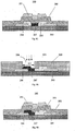
- Fig. 1 is a schematic sectional view of a thin film transistor 200 provided by an embodiment of the present disclosure.
- the thin film transistor is in a bottom-gate structure, a back channel etching structure for example.
- the thin film transistor 200 comprises a gate electrode 201, a gate insulating layer 202, an active layer 203 and a source-drain electrode layer (comprising a source electrode 204 and a drain electrode 205) which are sequentially stacked on a substrate.
- the active layer 203 comprises a surface 206 and the surface is in direct electrical contact with the source electrode 203 and the drain electrode 205.
- the surface may be a flat plane or comprise a concave surface portion.
- the concave surface portion is formed through an over-etching of the active layer 203 while forming the source-drain electrode layer with the back channel etching process, which is however not limited to the embodiment.
- the active layer 203 comprises a conductive region 207, and the conductive region 207 is located between the source electrode 204 and the drain electrode 205 and is spaced apart from at least one of the source electrode 204 and the drain electrode 205.
- the conductive region is spaced apart from both the source electrode 204 and the drain electrode 205.
- the conductive region 207 runs through the active layer 203 in a thickness direction of the active layer.
- the active layer of the thin film transistor 200 comprises two portions: a first channel region between the source electrode 204 and the conductive region 207, a length of which is L1; and a second channel region between the conductive region 207 and the drain electrode 205, a length of which is L2. Because of a provision of the conductive region 207, a channel length of the thin film transistor 200 is shortened from L to L1+L2.
- An on-current Ion of a thin film transistor Ion is positively proportional to a ratio of channel width W to channel length L of the thin film transistor.
- a value of Ion is positively proportional to the channel width W and is negatively proportional to the channel length L, so that a decrease in the channel length L of the thin film transistor can effectively increase the on-current of the thin film transistor.
- At least two technical benefits are achieved by providing of the conductive region 207: alleviating an interface characteristic degradation problem of the back channel etching surface of the active layer caused by over-etching, and decreasing the channel length of the thin film transistor 200 so as to increase the on-current of the thin film transistor.
- the conductive region 207 may be directly connected with the source electrode 204 and is only spaced apart from the drain electrode 205.
- the channel length of the thin film transistor is L'.
- the conductive region 207 is directly connected with the drain electrode 205 and is only spaced apart from the source electrode 204.
- the conductive region 207 may be a surface portion, which is close to a side of the source-drain electrode layer, of the active layer 203, that is, the conductive region 207 does not run through the active layer 203 in the thickness direction of the active layer 203.
- a material of the active layer may be a metal oxide semiconductor material, an amorphous silicon material, a polysilicon material or the like.
- the material of the active layer 203 may be indium gallium zinc oxide (IGZO), indium zinc oxide (IZO), zinc oxide (ZnO) or gallium zinc oxide (GZO) and the like.
- the polysilicon material may be high-temperature or low-temperature polysilicon or the like.
- the thin film transistor 200 may be in other bottom-gate structures.
- the source-drain electrode layer (comprising the source electrode 204 and the drain electrode 205) and the gate electrode 201 of the thin film transistor are located on a same side of the active layer 203.
- the thin film transistor 200 may be in a top-gate structure.
- the thin film transistor 200 comprises a source-drain electrode layer (comprising a source electrode 204 and a drain electrode 205), an active layer 203, a gate insulating layer 202 and a gate electrode 201 which are sequentially stacked on a substrate.
- Embodiments of the present disclosure further provide a manufacturing method of a thin film transistor, which may be used for manufacturing the thin film transistor of the above-mentioned embodiments.
- the method at least comprises: forming an active layer, a source electrode and a drain electrode; and performing a conducting treatment on a portion of the active layer to allow the portion to become a conductive region, wherein the conductive region is formed between the source electrode and the drain electrode and is spaced apart from at least one of the source electrode and the drain electrode.
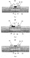
- Figs. 6A-6D are schematic sectional views of steps of a method for manufacturing a thin film transistor provided by an embodiment of the present disclosure.
- the method comprises the following steps:
- Step S61 forming the gate electrode 201.
- a substrate is firstly provided to form the thin film transistor thereon.
- the substrate may be exemplarily a glass substrate, a plastic substrate and the like.
- a cleaning operation and the like may be performed to the substrate firstly, and a buffer layer may also be formed on the substrate and then the thin film transistor is formed on the buffer layer.
- the buffer layer can prevent impurity ions in the substrate from diffusing into the thin film transistor and therefor causing a performance of the thin film transistor to decrease.
- a first conductive layer is formed on the substrate and a first patterning process is performed on the first conductive layer to pattern the first conductive layer to form the gate electrode 201.
- the first conductive layer is a metal layer for example, a material of which may be aluminum or aluminum alloy, copper or copper alloy or the like.
- the substrate may be a bendable flexible substrate, for example, a substrate made of various kinds of plastic films such as polyethylene terephthalate (PET), polyether sulfone (PES), polycarbonate (PC) polyimide (PI) or derivative of the above.
- PET polyethylene terephthalate
- PES polyether sulfone
- PC polycarbonate
- PI polyimide
- Step S62 forming the gate insulating layer 202 and the active layer 203.
- the gate insulating layer 202 is formed on the gate electrode 201, subsequently a semiconductor layer is formed on the gate insulating layer 202, and the active layer 203 is formed using a second patterning process to pattern the semiconductor layer.
- a material of the active layer 203 may be a semiconductor material such as a metal oxide semiconductor material, an amorphous silicon material, a polysilicon material and the like.
- the material of the active layer 203 may be metal oxide semiconductor materials such as indium gallium zinc oxide (IGZO), indium zinc oxide (IZO), zinc oxide (ZnO) or gallium zinc oxide (GZO).
- the polysilicon material may be high-temperature or low-temperature polysilicon.
- a material of the gate insulating layer may be an inorganic insulating layer such as silicon oxide, silicon nitride, silicon oxynitride and the like.
- Step S63 forming the source electrode 204 and the drain electrode 205.
- a second conductive layer is formed on the active layer 203, and a third patterning process is used to pattern the second conductive layer to form the source electrode 204 and the drain electrode 205.
- the second conductive layer may be exemplarily selected from metal materials such as molybdenum, titanium, copper and alloy of them.
- the third patterning process may be a photolithography process comprising exposure, development and etching and the like.
- an over-etching is usually performed to etch away a portion of a back surface of the active layer 203, so that a concave surface 206 is formed in the back surface of the active layer 203. Because a material of the active layer 203 is sensitive to the etching gases or solutions, a semiconductor characteristic of the active layer 203 at the concave surface is adversely affected, and non-uniform etching, interface defects and the like may be formed for example.
- Step S64 forming the conductive region 207.
- a photoresist layer is formed on the source electrode 204 and the drain electrode 205, which covers the source electrode 204 and the drain electrode 205.
- the photoresist layer is exposed and developed to form a mask layer 209 with an opening 208.
- the opening 208 is disposed to correspond to a portion between the source electrode 204 and the drain electrode 205 and to expose at least a portion of the active layer 203.
- the source electrode 204 and the drain electrode 205 are both covered by the mask layer 209, that is, not exposed by the opening 208.
- a location of the opening 208 such as a distance between the opening 208 and the source electrode 204 and the drain electrode 205 is not precisely required by the embodiment of the present disclosure, a requirement for an exposure process precision in this step is low, and the opening 208 is only needed to be formed to correspond to a portion between the source electrode 204 and the drain electrode 205.
- a distance between the source electrode 204 and the drain electrode 205 is defined as L, a size of the opening 208 is L3, and a value range of L3 may be 0 ⁇ L3 ⁇ L for example.
- the mask layer 209 is used to perform a conduction process to the active layer 203 to form the conductive region 207.
- the conductive region 207 is spaced apart from both the source electrode 204 and the drain electrode 205.
- a manner of the conduction process may be selected according to a material of the active layer, exemplarily comprising a plasma treatment to the active layer 203.
- the conductive region 207 runs through the active layer in a thickness direction of the active layer 203.
- condition parameters such as a gas concentration, a process time, a power and the like used during the plasma treatment may be controlled, so as to allow the conductive region 207 to be only a surface portion, which is close to a side of the source-drain electrode layer, of the active layer 203, and not to run through the active layer 203 in the thickness direction of the active layer.
- An off-current is usually smaller in this type of structure.
- the channel region of the thin film transistor 200 comprises two portions: a first channel region between the source electrode 204 and the conductive region 207, of which a length is L1; and a second channel region between the conductive region 207 and the drain electrode 205, of which a length is L2. Because of a formation of the conductive region 207, a channel length of the thin film transistor 200 is shortened from L without the conductive region 207 to L1+L2 with the conductive region 207.
- IGZO indium gallium zinc oxide
- gases for forming the plasma comprise gases containing hydrogen elements, such as hydrogen gas (H2), ammonia gas (NH3), silane (SiH4). These gases are ionized into hydrogen ions which enter into the active layer during the plasma treatment, so that the hydrogen concentration of the active layer is increased and a conductivity of the active layer is improved.
- H2 hydrogen gas
- NH3 ammonia gas
- SiH4 silane
- gases for forming the plasma comprise inert gases with an atom radius smaller than an oxygen ion radius, such as helium gas.
- the oxygen concentration of the active layer can be reduced by bombarding the oxygen ions in the active layer using the helium atoms, so as to improve the conductivity of the active layer.
- the mask layer 209 is removed finally, so as to form the thin film transistor 200 with the back channel etching structure as illustrated in Fig. 1 .
- the opening 208 of the mask layer 209 exposes at least a portion of one of the source electrode 204 and the drain electrode 205.
- the opening 208 exposes at least a portion of the source electrode 204.
- the conductive region 207 is directly connected with the source electrode 204, so that the thin film transistor 200 as illustrated in Fig. 2 is formed.
- a requirement for a precision of the size L3 of the opening 208 is lower, and it is only needed to ensure that one of the source electrode and the drain electrode is exposed through the opening and the other is not exposed through the opening.
- At least two technical benefits are achieved by providing the conductive region in the active layer of the thin film transistor: alleviating an interface characteristic degradation problem of the back channel etching surface of the active layer caused by over-etching, and decreasing the channel length of the thin film transistor 200 so as to increase the on-current of the thin film transistor.
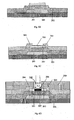
- Figs. 8A-8C are schematic sectional views of steps of a method for manufacturing a thin film transistor provided by another embodiment of the present disclosure.
- the method comprises the following steps:
- Step S81 forming the source electrode 204 and the drain electrode 205.
- a substrate is firstly provided to form the thin film transistor thereon.
- the substrate may be exemplarily a rigid substrate or a flexible substrate, may be a glass substrate, a plastic substrate and the like.
- a first conductive layer is formed on the substrate and a first patterning process is performed on the first conductive layer to pattern the first conductive layer to form the source electrode 204 and the drain electrode 205.
- the first patterning process may be a photolithography process comprising exposure, development and etching and the like.
- the first conductive layer may be exemplarily selected from materials such as molybdenum, titanium, aluminum, copper and alloy of them.
- Step S82 forming the active layer 203 and the conductive region 207 of the active layer 203.
- a semiconductor layer is formed on the source electrode 204 and the drain electrode 205, and the active layer 203 is formed by using a second patterning process to pattern the second semiconductor layer.
- a material of the active layer 203 may be a semiconductor material such as a metal oxide semiconductor material, an amorphous silicon material, a polysilicon material or the like.
- the material of the active layer 203 may be metal oxide semiconductor materials such as indium gallium zinc oxide (IGZO), indium zinc oxide (IZO), zinc oxide (ZnO) or gallium zinc oxide (GZO) and the like.
- a photoresist layer is formed on the source electrode 204 and the drain electrode 205.
- the photoresist layer is exposed and developed to form a mask layer 209 with an opening 208.
- the opening 208 is disposed to correspond to a portion between the source electrode 204 and the drain electrode 205.
- a location of the opening 208 such as a distance between the opening 208 and the source electrode 204 and the drain electrode 205 may be not precisely required by the embodiment of the present disclosure, a requirement for an exposure process precision in this step is low, and the opening 208 is only needed to be formed corresponding between the source electrode 204 and the drain electrode 205.
- a distance between the source electrode 204 and the drain electrode 205 is defined as L, a size of the opening 208 is L3, and a value range of L3 may be 0 ⁇ L3 ⁇ L for example.
- the mask layer 209 is used to perform a conduction process to the active layer 203 to form the conductive region 207.
- the conductive region 207 is spaced apart from both the source electrode 204 and the drain electrode 205, and the conductive region 207 runs through the active layer in a thickness direction of the active layer 203.
- the channel region of the obtained thin film transistor 200 comprises two portions: a first channel region between the source electrode 204 and the conductive region 207, of which a length is L1; and a second channel region between the conductive region 207 and the drain electrode 205, of which a length is L2. Because of a formation of the conductive region 207, a channel length of the thin film transistor 200 is shortened from L without the conductive region 207 to L1+L2 with the conductive region 207.
- IGZO indium gallium zinc oxide
- gases for forming the plasma comprise gases containing hydrogen elements, such as hydrogen gas (H2), ammonia gas (NH3), silane (SiH4). These gases are ionized into hydrogen ions which enter into the active layer during the plasma treatment, so that the hydrogen concentration of the active layer is increased and a conductivity of the active layer is improved.
- H2 hydrogen gas
- NH3 ammonia gas
- SiH4 silane
- gases for forming the plasma comprise inert gases, of which an atom radius is smaller than an oxygen ion radius, such as helium gas.
- the oxygen concentration of the active layer can be reduced by bombarding the oxygen ions in the active layer using the helium atoms, so as to improve the conductivity of the active layer.
- the mask layer 209 is removed after forming the conductive region 207.
- Step S83 forming the gate insulating layer 202 and the gate electrode 201.
- the gate insulating layer 202 is formed on the active layer 203, a second conductive layer is formed on the gate insulating layer 202, and a third pattering process is used to pattern the second conductive layer to form the gate electrode 202.
- a material of the gate insulating layer may be an inorganic insulating layer such as silicon oxide, silicon nitride, silicon oxynitride and the like.
- the second conductive layer may be exemplarily selected from materials such as molybdenum, titanium, aluminum, copper and alloy of them.
- the top-gate thin film transistor 200 with a top-gate structure as illustrated in Fig. 5 is formed.
- a projection of the opening 208 of the mask layer 209 on the substrate is at least partially overlapped with a projection of one of the source electrode 204 and the drain electrode 205 on the substrate.
- the projection of the opening 208 of the mask layer 209 on the substrate is partially overlapped with the projection of the source electrode 204 on the substrate.
- the conductive region 207 formed in this situation is directly connected with the source electrode 204, so that the thin film transistor 200 as illustrated in Fig. 9B is formed.
- the conductive region is formed in the active layer of the thin film transistor, so that the channel length of the thin film transistor is reduced and thereby the on-current of the thin film transistor is increased.
- top-gate or bottom-gate thin film transistor with other structures may be formed, which is not repeated here.
- Embodiments of the present disclosure further provide an array substrate and the array substrate may be applied in a liquid crystal display device, an organic light-emitting diode display device or an e-paper display device and the like.
- the array substrate may comprise the thin film transistor according to any one embodiment of the present disclosure.
- the array substrate of the embodiment comprises a plurality of gate lines and a plurality of data lines. These gate lines and data lines intersect with each other, thereby defining pixel units arranged in an array.
- Each pixel unit comprises a thin film transistor functioning as a switch element and a pixel electrode connected with the thin film transistor.
- a gate electrode of the thin film transistor of each pixel is electrically connected with a corresponding gate line or is formed integrally with the corresponding gate line
- a drain electrode is electrically connected with a corresponding data line or is formed integrally with the corresponding data line.
- the thin film transistor may adopt the thin film transistor according to any one embodiment of the present disclosure.
- the pixel electrode of each pixel unit is configured to apply an electric field to control a rotation degree of liquid crystal molecules so as to achieve the display.
- the pixel electrode of each pixel unit functions as an anode or a cathode to drive an organic light-emitting material to emit light so as to achieve the display.
- the pixel electrode of each pixel unit is configured to apply a voltage to drive charged particles in electronic ink to move so as to achieve the display.
- the array substrate 300 comprises the thin film transistor 200 as illustrated in Fig. 1 , and further comprises a planarization layer or a passivation layer 201 on the thin film transistor.
- the pixel electrode 211 is connected with the source electrode 204 through a through hole running through the planarization layer or the passivation layer.
- the drain electrode 205 of the thin film transistor is connected with the data line (not shown).
- the thin film transistor functions as a switch element, controlling a signal transmission between the data line and the pixel electrode 211.
- Embodiments of the present disclosure further provide an electronic device 400, and the electronic device comprises the thin film transistor 200 according to any one embodiment of the present disclosure or the above-mentioned array substrate 300.
- the electronic device is a display device such as a liquid crystal display device, an organic light-emitting diode display device and an e-paper display device.
- a pixel unit of the display device comprises the thin film transistor 200.
- a driving circuit of the display device comprises the thin film transistor 200.
- the thin film transistor of the above mentioned pixel unit or driving circuit i. e. GOA
- GOA driving circuit
- Fig. 11 is a schematic diagram of an electronic device 400 provided by an embodiment of the present disclosure
- Fig. 12 is schematic view of a pixel circuit of the electronic device of Fig. 11 .
- the electronic device 400 is an organic light-emitting diode display device.
- the organic light-emitting diode display device comprises a plurality of pixel units 401 arranged in an array, each pixel unit 401 comprises at least one organic light-emitting diode and a pixel circuit connected with the organic light-emitting diode, and the organic light-emitting diode is driven to emit light by the pixel circuit.
- Fig. 12 is a schematic view of a 2T1C pixel circuit of an organic light-emitting diode electronic device.
- the pixel circuit comprises a switch transistor T1, a driving transistor T2 and a storage capacitor Cs.
- a gate electrode of the switch transistor T1 is connected with a gate line to receive a scan signal (Scan), a source electrode is connected with a data line to receive a data signal (Vdata) for example, and a drain electrode is connected with a gate electrode of the driving transistor T2.
- a source electrode of the driving transistor T2 is connected with a first power source terminal (Vdd, a high voltage terminal) and a drain electrode is connected with a positive end of OLED.
- a driving manner of the 2T1C pixel circuit is to control bright and dark (a greyscale) of a pixel by two TFTs and a storage capacitor Cs.
- the data voltage (Vdata) which is sent through the data line by a data driving circuit charges the storage capacitor Cs through the switch transistor T1, so as to store the data voltage in the storage capacitor Cs.
- the stored data voltage controls a conduction degree of the driving transistor T2 so as to control a current value of current which runs through the driving transistor to drive the OLED to emit light; that is, the current determines an emission greyscale of the OLED.
- the switch transistor T1 and the driving transistor T2 both may adopt the thin film transistor 200 of the embodiments of the present disclosure for example.
- the organic light-emitting diode display device may further comprise a data driving circuit 6 and a gate driving circuit 7.
- the data driving circuit 6 is configured to provide a data signal and the gate driving circuit 7 is configured to provide a scan signal (e. g. the signal Vscan) and may be further configured to provide various kinds of control signals.
- the data driving circuit 6 is electrically connected with the pixel unit 401 through the data line 61, and the gate driving circuit 7 is electrically connected with the pixel unit 401 through the gate line 71.
- the data driving circuit 6 and the gate driving circuit 7 both comprises a thin film transistor which may adopt the thin film transistor 200 of the embodiments of the present disclosure for example.
- the display device may be applied in any product or component having display functions such as a cellphone, a tablet computer, a television, a displayer, a notebook computer, a digital photo frame, a navigator and the like.
Landscapes
- Engineering & Computer Science (AREA)
- Power Engineering (AREA)
- Microelectronics & Electronic Packaging (AREA)
- Physics & Mathematics (AREA)
- Condensed Matter Physics & Semiconductors (AREA)
- General Physics & Mathematics (AREA)
- Computer Hardware Design (AREA)
- Ceramic Engineering (AREA)
- Manufacturing & Machinery (AREA)
- Chemical & Material Sciences (AREA)
- Crystallography & Structural Chemistry (AREA)
- Thin Film Transistor (AREA)
Abstract
Description
- Embodiments of the present disclosure relate to a thin film transistor and a manufacturing method thereof and an electronic device.
- A display device of an active matrix (AM) type becomes a mainstream product of the current display devices due to its advantages such as high resolution, rapid response speed and high contrast and the like, which comprises an organic light-emitting diode (OLED) display device, a liquid crystal display device (LCD) and the like. A thin film transistor (TFT) is an important element in the active matrix display device, which can function as a switching element or a driving element. A structure and a manufacturing process of the thin film transistor both exert a great influence on the performance of the display device.
- Embodiments of the present disclosure provide a thin film transistor, comprising: an active layer, a source electrode and a drain electrode. The active layer comprises a conductive region, and the conductive region is between the source electrode and the drain electrode and is spaced apart from at least one of the source electrode and the drain electrode.
- For example, the conductive region is spaced apart from both the source electrode and the drain electrode.
- For example, the conductive region is directly connected with the source electrode and a channel region is between the conductive region and the drain electrode; or the conductive region is directly connected with the drain electrode and a channel region is between the conductive region and the source electrode.
- For example, the conductive region runs through the active layer in a thickness direction of the active layer.
- For example, the thin film transistor is in a top-gate structure or a bottom-gate structure.
- For example, the thin film transistor comprises a back channel etching structure and the conductive region corresponds to a surface of the back channel etching structure.
- For example, a material of the active layer is a metal oxide semiconductor material, an amorphous silicon material or a polysilicon material.
- For example, the metal oxide semiconductor material comprises indium gallium zinc oxide (IGZO), indium zinc oxide (IZO), zinc oxide (ZnO) or gallium zinc oxide (GZO).
- Embodiments of the present disclosure further provide an array substrate , comprising the above mentioned thin film transistor.
- Embodiments of the present disclosure further provide an electronic device, comprising the above mentioned thin film transistor or array substrate.
- For example, the electronic device is a liquid crystal display device, an organic light emitting diode display device or an e-paper display device.
- Embodiments of the present disclosure further provide a manufacturing method of a thin film transistor, comprising: forming an active layer, a source electrode and a drain electrode; and performing a conduction treatment on a portion of the active layer to allow the portion to become a conductive region. The conductive region is formed between the source electrode and the drain electrode and is spaced apart from at least one of the source electrode and the drain electrode.
- For example, the conduction treatment comprises: forming a mask layer with an opening on the active layer, the opening exposing at least a portion of the active layer; and performing the conduction treatment on the active layer using the mask layer.
- For example, a source-drain electrode layer is formed after forming the active layer and before forming the mask layer, and a patterning process is performed on the source-drain electrode layer to form the source electrode and the drain electrode.
- For example, the conduction treatment comprises performing a plasma treatment on the active layer.
- In order to clearly illustrate the technical solution of the embodiments of the invention, the drawings of the embodiments will be briefly described in the following; it is obvious that the described drawings are only related to some embodiments of the invention and thus are not limitative of the invention.
-
Fig. 1 is a schematic sectional view of a thin film transistor provided by an embodiment of the present disclosure; -
Fig. 2 is a schematic sectional view of a thin film transistor provided by a modified embodiment of the present disclosure; -
Fig. 3 is a schematic sectional view of a thin film transistor provided by another modified embodiment of the present disclosure; -
Fig. 4 is a schematic sectional view of a thin film transistor provided by still another modified embodiment of the present disclosure; -
Fig. 5 is a schematic sectional view of a thin film transistor provided by still further another modified embodiment of the present disclosure; -
Figs. 6A-6D are schematic sectional views of steps of a method for manufacturing a thin film transistor provided by an embodiment of the present disclosure; -
Fig. 7 is a schematic sectional view of steps of a method for manufacturing a thin film transistor provided by a modified embodiment of the present disclosure; -
Figs. 8A-8C are schematic sectional views of steps of a method for manufacturing a thin film transistor provided by another embodiment of the present disclosure; -
Figs. 9A-9B are schematic sectional views of steps of a method for manufacturing a thin film transistor provided by a modified embodiment of the present disclosure; -
Fig. 10 is a schematic view of an array substrate provided by an embodiment of the present disclosure; -
Fig. 11 is a schematic view of an electronic device provided by an embodiment of the present disclosure; and -
Fig. 12 is a schematic view of a 2T1C pixel circuit of the electronic device inFig. 11 . - In order to make objects, technical details and advantages of the embodiments of the disclosure apparent, the technical solutions of the embodiments will be described in a clearly and fully understandable way in connection with the drawings related to the embodiments of the disclosure. Apparently, the described embodiments are just a part but not all of the embodiments of the disclosure. Based on the described embodiments herein, those skilled in the art can obtain other embodiment(s), without any inventive work, which should be within the scope of the disclosure.
- Unless otherwise defined, all the technical and scientific terms used herein have the same meanings as commonly understood by one of ordinary skill in the art to which the present disclosure belongs. The terms "first," "second," etc., which are used in the description and the claims of the present application for disclosure, are not intended to indicate any sequence, amount or importance, but distinguish various components. Also, the terms such as "a," "an," etc., are not intended to limit the amount, but indicate the existence of at least one. The terms "comprise," "comprising," "include," "including," etc., are intended to specify that the elements or the objects stated before these terms encompass the elements or the objects and equivalents thereof listed after these terms, but do not preclude the other elements or objects. The phrases "connect", "connected", etc., are not intended to define a physical connection or mechanical connection, but may include an electrical connection, directly or indirectly. "On," "under," "right," "left" and the like are only used to indicate relative position relationship, and when the position of the object which is described is changed, the relative position relationship may be changed accordingly.
- In the middle of the twentieth century, oxide ZnO thin film transistor (TFT) was extensively researched but not widely applied due to limitations of itself. Until 2003, indium gallium zinc oxide thin film transistors (IGZO TFT) attracted great attentions for outstanding performances. From then, oxide thin film transistor technologies have entered into a rapid development phase. A metal oxide thin film transistor adopts a metal oxide semiconductor material as the active layer to provide a channel. These materials mainly comprise n-type semiconductor materials based on zinc oxide and/or indium oxide and the like, such as zinc oxide (ZnO), indium oxide (In2O3), zinc indium oxide (IZO), aluminum doped zinc oxide (AZO), boron doped zinc oxide (BZO), magnesium doped zinc oxide (MZO), zinc tin oxide (ZTO), indium gallium zinc oxide (IGZO), indium tin zinc oxide (ITZO), gallium zinc oxide (GZO), indium tin oxide (ITO), hafnium indium zinc oxide (HIZO), tin oxide (SnO2) and the like; and p-type semiconductor materials such as stannous oxide (SnO), cuprous oxide (Cu2O) and the like. Compared to a silicon-based (amorphous silicon, polysilicon and the like) thin film transistor, the metal oxide thin film transistor has obvious advantages mainly including a higher mobility, a steeper sub-threshold swing, a smaller off-state leakage current, a better uniformity in device performance, a simple process, a low process temperature, a good stability, a high light transmittance, no obvious degradation in device performance in a curved state and the like.
- During a manufacturing process of an amorphous silicon thin film transistor, a common source-drain etching solution or gas does little etching damage to an active region of the amorphous silicon and a performance of the device barely degrades before and after the source-drain is etched, so a photolithography process may be directly adopted for an amorphous silicon thin film transistor to form a source-drain electrode and a wiring layer and the like above the active region, which is called a back-channel etching (BCE) process and can achieve aims such as simplifying process, reducing cost and the like. However, for an oxide thin film transistor represented by indium gallium zinc oxide thin film transistor, the oxide semiconductor layer is very sensitive to acidic or alkaline etching solution and gas. If a back-channel etching process similar to the amorphous silicon thin film transistor process is adopted to manufacture the oxide thin film transistor, a back interface characteristics of the active region of the oxide thin film transistor may be damaged by the source-drain etching solution or gas and the performance of the device degrades obviously.
- A back channel etch-stop layer (ESL) process may be used to solve the problem that a device characteristic is influenced by the source-drain etching process. Although the process can bring an obvious improvement to the device characteristic, additional deposition, photolithography and etching steps are required to form the etch-stop layer, which obviously increase process complexity and cost. Therefore, if the etch-stop layer process is adopted to form the oxide thin film transistor, cost can be obviously higher than that of an oxide thin film transistor or an amorphous silicon thin film transistor made by the back-channel etching process.
- Embodiments of the present disclosure provide a thin film transistor and a manufacturing method thereof and an electronic device. The thin film transistor provides a conductive region in a portion, which is between the source electrode and the drain electrode, of the active layer of the thin film transistor, so as not only to improve an interface performance of the thin film transistor, but also to decrease a channel length of the thin film transistor. In this way, an on-state current is increased.
- Specific embodiments of the present disclosure are described below in connection with the figures so as to make the present disclosure better understood.
-
Fig. 1 is a schematic sectional view of athin film transistor 200 provided by an embodiment of the present disclosure. The thin film transistor is in a bottom-gate structure, a back channel etching structure for example. Thethin film transistor 200 comprises agate electrode 201, agate insulating layer 202, anactive layer 203 and a source-drain electrode layer (comprising asource electrode 204 and a drain electrode 205) which are sequentially stacked on a substrate. Theactive layer 203 comprises asurface 206 and the surface is in direct electrical contact with thesource electrode 203 and thedrain electrode 205. The surface may be a flat plane or comprise a concave surface portion. The concave surface portion is formed through an over-etching of theactive layer 203 while forming the source-drain electrode layer with the back channel etching process, which is however not limited to the embodiment. Theactive layer 203 comprises aconductive region 207, and theconductive region 207 is located between thesource electrode 204 and thedrain electrode 205 and is spaced apart from at least one of thesource electrode 204 and thedrain electrode 205. For example, as illustrated in the figure, the conductive region is spaced apart from both thesource electrode 204 and thedrain electrode 205. For example, theconductive region 207 runs through theactive layer 203 in a thickness direction of the active layer. In this embodiment, the active layer of thethin film transistor 200 comprises two portions: a first channel region between thesource electrode 204 and theconductive region 207, a length of which is L1; and a second channel region between theconductive region 207 and thedrain electrode 205, a length of which is L2. Because of a provision of theconductive region 207, a channel length of thethin film transistor 200 is shortened from L to L1+L2. - An on-current Ion of a thin film transistor Ion is positively proportional to a ratio of channel width W to channel length L of the thin film transistor. For example, in a case that the thin film transistor works in a saturation region, a calculation formula of the on-current Ion is as follows:

- As can be seen, a value of Ion is positively proportional to the channel width W and is negatively proportional to the channel length L, so that a decrease in the channel length L of the thin film transistor can effectively increase the on-current of the thin film transistor.
- In this embodiment, at least two technical benefits are achieved by providing of the conductive region 207: alleviating an interface characteristic degradation problem of the back channel etching surface of the active layer caused by over-etching, and decreasing the channel length of the
thin film transistor 200 so as to increase the on-current of the thin film transistor. - In a modified embodiment, for example, as illustrated in
Fig. 2 , theconductive region 207 may be directly connected with thesource electrode 204 and is only spaced apart from thedrain electrode 205. In this situation, the channel length of the thin film transistor is L'. Or, theconductive region 207 is directly connected with thedrain electrode 205 and is only spaced apart from thesource electrode 204. - In a modified embodiment, for example, as illustrated in
Fig. 3 , theconductive region 207 may be a surface portion, which is close to a side of the source-drain electrode layer, of theactive layer 203, that is, theconductive region 207 does not run through theactive layer 203 in the thickness direction of theactive layer 203. - For example, a material of the active layer may be a metal oxide semiconductor material, an amorphous silicon material, a polysilicon material or the like.
- For example, the material of the
active layer 203 may be indium gallium zinc oxide (IGZO), indium zinc oxide (IZO), zinc oxide (ZnO) or gallium zinc oxide (GZO) and the like. The polysilicon material may be high-temperature or low-temperature polysilicon or the like. - In a modified embodiment, for example, the
thin film transistor 200 may be in other bottom-gate structures. As illustrated inFig. 4 , the source-drain electrode layer (comprising thesource electrode 204 and the drain electrode 205) and thegate electrode 201 of the thin film transistor are located on a same side of theactive layer 203. - In a modified embodiment, for example, the
thin film transistor 200 may be in a top-gate structure. As illustrated inFig. 5 , thethin film transistor 200 comprises a source-drain electrode layer (comprising asource electrode 204 and a drain electrode 205), anactive layer 203, agate insulating layer 202 and agate electrode 201 which are sequentially stacked on a substrate. - Embodiments of the present disclosure further provide a manufacturing method of a thin film transistor, which may be used for manufacturing the thin film transistor of the above-mentioned embodiments. The method at least comprises: forming an active layer, a source electrode and a drain electrode; and performing a conducting treatment on a portion of the active layer to allow the portion to become a conductive region, wherein the conductive region is formed between the source electrode and the drain electrode and is spaced apart from at least one of the source electrode and the drain electrode.
-
Figs. 6A-6D are schematic sectional views of steps of a method for manufacturing a thin film transistor provided by an embodiment of the present disclosure. For the bottom-gate thin film transistor as illustrated inFig. 1 , the method comprises the following steps: - Step S61, forming the
gate electrode 201. - As illustrated in
Fig. 6A , a substrate is firstly provided to form the thin film transistor thereon. The substrate may be exemplarily a glass substrate, a plastic substrate and the like. A cleaning operation and the like may be performed to the substrate firstly, and a buffer layer may also be formed on the substrate and then the thin film transistor is formed on the buffer layer. The buffer layer can prevent impurity ions in the substrate from diffusing into the thin film transistor and therefor causing a performance of the thin film transistor to decrease. A first conductive layer is formed on the substrate and a first patterning process is performed on the first conductive layer to pattern the first conductive layer to form thegate electrode 201. The first conductive layer is a metal layer for example, a material of which may be aluminum or aluminum alloy, copper or copper alloy or the like. - Additionally, the substrate may be a bendable flexible substrate, for example, a substrate made of various kinds of plastic films such as polyethylene terephthalate (PET), polyether sulfone (PES), polycarbonate (PC) polyimide (PI) or derivative of the above.
- Step S62, forming the
gate insulating layer 202 and theactive layer 203. - As illustrated in
Fig. 6B , thegate insulating layer 202 is formed on thegate electrode 201, subsequently a semiconductor layer is formed on thegate insulating layer 202, and theactive layer 203 is formed using a second patterning process to pattern the semiconductor layer. - A material of the
active layer 203 may be a semiconductor material such as a metal oxide semiconductor material, an amorphous silicon material, a polysilicon material and the like. For example, the material of theactive layer 203 may be metal oxide semiconductor materials such as indium gallium zinc oxide (IGZO), indium zinc oxide (IZO), zinc oxide (ZnO) or gallium zinc oxide (GZO). The polysilicon material may be high-temperature or low-temperature polysilicon. A material of the gate insulating layer may be an inorganic insulating layer such as silicon oxide, silicon nitride, silicon oxynitride and the like. - Step S63, forming the
source electrode 204 and thedrain electrode 205. - As illustrated in
Fig. 6C , a second conductive layer is formed on theactive layer 203, and a third patterning process is used to pattern the second conductive layer to form thesource electrode 204 and thedrain electrode 205. The second conductive layer may be exemplarily selected from metal materials such as molybdenum, titanium, copper and alloy of them. - The third patterning process may be a photolithography process comprising exposure, development and etching and the like. During the process of etching the second conductive layer to form the source electrode and the drain electrode which are spaced apart from each other at a predetermined distance so as to be insulated from each other, in order to prevent a short circuit from occurring between the source electrode and the drain electrode due to a halfway etching, an over-etching is usually performed to etch away a portion of a back surface of the
active layer 203, so that aconcave surface 206 is formed in the back surface of theactive layer 203. Because a material of theactive layer 203 is sensitive to the etching gases or solutions, a semiconductor characteristic of theactive layer 203 at the concave surface is adversely affected, and non-uniform etching, interface defects and the like may be formed for example. - Step S64, forming the
conductive region 207. - As illustrated in
Fig. 6D , a photoresist layer is formed on thesource electrode 204 and thedrain electrode 205, which covers thesource electrode 204 and thedrain electrode 205. The photoresist layer is exposed and developed to form amask layer 209 with anopening 208. In this embodiment, theopening 208 is disposed to correspond to a portion between thesource electrode 204 and thedrain electrode 205 and to expose at least a portion of theactive layer 203. As illustrated in the figure, thesource electrode 204 and thedrain electrode 205 are both covered by themask layer 209, that is, not exposed by theopening 208. Because a location of theopening 208 such as a distance between theopening 208 and thesource electrode 204 and thedrain electrode 205 is not precisely required by the embodiment of the present disclosure, a requirement for an exposure process precision in this step is low, and theopening 208 is only needed to be formed to correspond to a portion between thesource electrode 204 and thedrain electrode 205. A distance between thesource electrode 204 and thedrain electrode 205 is defined as L, a size of theopening 208 is L3, and a value range of L3 may be 0 < L3 < L for example. - Subsequently, the
mask layer 209 is used to perform a conduction process to theactive layer 203 to form theconductive region 207. For example, theconductive region 207 is spaced apart from both thesource electrode 204 and thedrain electrode 205. In this embodiment, a manner of the conduction process may be selected according to a material of the active layer, exemplarily comprising a plasma treatment to theactive layer 203. In this embodiment, theconductive region 207 runs through the active layer in a thickness direction of theactive layer 203. In other embodiments, condition parameters such as a gas concentration, a process time, a power and the like used during the plasma treatment may be controlled, so as to allow theconductive region 207 to be only a surface portion, which is close to a side of the source-drain electrode layer, of theactive layer 203, and not to run through theactive layer 203 in the thickness direction of the active layer. An off-current is usually smaller in this type of structure. - In this embodiment, the channel region of the
thin film transistor 200 comprises two portions: a first channel region between thesource electrode 204 and theconductive region 207, of which a length is L1; and a second channel region between theconductive region 207 and thedrain electrode 205, of which a length is L2. Because of a formation of theconductive region 207, a channel length of thethin film transistor 200 is shortened from L without theconductive region 207 to L1+L2 with theconductive region 207. - For example, for an indium gallium zinc oxide (IGZO) active layer, there are two ways to perform a conduction process on the
active layer 203 through the plasma treatment: increasing a hydrogen concentration of the active layer, or reducing an oxygen concentration of the active layer. - For example, gases for forming the plasma comprise gases containing hydrogen elements, such as hydrogen gas (H2), ammonia gas (NH3), silane (SiH4). These gases are ionized into hydrogen ions which enter into the active layer during the plasma treatment, so that the hydrogen concentration of the active layer is increased and a conductivity of the active layer is improved.
- For example, gases for forming the plasma comprise inert gases with an atom radius smaller than an oxygen ion radius, such as helium gas. The oxygen concentration of the active layer can be reduced by bombarding the oxygen ions in the active layer using the helium atoms, so as to improve the conductivity of the active layer.
- The
mask layer 209 is removed finally, so as to form thethin film transistor 200 with the back channel etching structure as illustrated inFig. 1 . - In a modified embodiment, the
opening 208 of themask layer 209 exposes at least a portion of one of thesource electrode 204 and thedrain electrode 205. For example, as illustrated inFig. 7 , theopening 208 exposes at least a portion of thesource electrode 204. In this situation, theconductive region 207 is directly connected with thesource electrode 204, so that thethin film transistor 200 as illustrated inFig. 2 is formed. In this embodiment, a requirement for a precision of the size L3 of theopening 208 is lower, and it is only needed to ensure that one of the source electrode and the drain electrode is exposed through the opening and the other is not exposed through the opening. - In this embodiment and the modified embodiment thereof, at least two technical benefits are achieved by providing the conductive region in the active layer of the thin film transistor: alleviating an interface characteristic degradation problem of the back channel etching surface of the active layer caused by over-etching, and decreasing the channel length of the
thin film transistor 200 so as to increase the on-current of the thin film transistor. -
Figs. 8A-8C are schematic sectional views of steps of a method for manufacturing a thin film transistor provided by another embodiment of the present disclosure. For the top-gate thin film transistor as illustrated inFig. 5 , the method comprises the following steps: - Step S81, forming the
source electrode 204 and thedrain electrode 205. - As illustrated in
Fig. 8A , a substrate is firstly provided to form the thin film transistor thereon. The substrate may be exemplarily a rigid substrate or a flexible substrate, may be a glass substrate, a plastic substrate and the like. A first conductive layer is formed on the substrate and a first patterning process is performed on the first conductive layer to pattern the first conductive layer to form thesource electrode 204 and thedrain electrode 205. The first patterning process may be a photolithography process comprising exposure, development and etching and the like. The first conductive layer may be exemplarily selected from materials such as molybdenum, titanium, aluminum, copper and alloy of them. - Step S82, forming the
active layer 203 and theconductive region 207 of theactive layer 203. - As illustrated in
Fig. 8B , a semiconductor layer is formed on thesource electrode 204 and thedrain electrode 205, and theactive layer 203 is formed by using a second patterning process to pattern the second semiconductor layer. - A material of the
active layer 203 may be a semiconductor material such as a metal oxide semiconductor material, an amorphous silicon material, a polysilicon material or the like. For example, the material of theactive layer 203 may be metal oxide semiconductor materials such as indium gallium zinc oxide (IGZO), indium zinc oxide (IZO), zinc oxide (ZnO) or gallium zinc oxide (GZO) and the like. - Subsequently, a photoresist layer is formed on the
source electrode 204 and thedrain electrode 205. The photoresist layer is exposed and developed to form amask layer 209 with anopening 208. In this embodiment, theopening 208 is disposed to correspond to a portion between thesource electrode 204 and thedrain electrode 205. A location of theopening 208 such as a distance between theopening 208 and thesource electrode 204 and thedrain electrode 205 may be not precisely required by the embodiment of the present disclosure, a requirement for an exposure process precision in this step is low, and theopening 208 is only needed to be formed corresponding between thesource electrode 204 and thedrain electrode 205. A distance between thesource electrode 204 and thedrain electrode 205 is defined as L, a size of theopening 208 is L3, and a value range of L3 may be 0 < L3 < L for example. - Subsequently, the
mask layer 209 is used to perform a conduction process to theactive layer 203 to form theconductive region 207. Theconductive region 207 is spaced apart from both thesource electrode 204 and thedrain electrode 205, and theconductive region 207 runs through the active layer in a thickness direction of theactive layer 203. - The channel region of the obtained
thin film transistor 200 comprises two portions: a first channel region between thesource electrode 204 and theconductive region 207, of which a length is L1; and a second channel region between theconductive region 207 and thedrain electrode 205, of which a length is L2. Because of a formation of theconductive region 207, a channel length of thethin film transistor 200 is shortened from L without theconductive region 207 to L1+L2 with theconductive region 207. - For example, for an indium gallium zinc oxide (IGZO) active layer, there are two ways to perform a conduction process on the
active layer 203 through the plasma treatment: increasing a hydrogen concentration of the active layer, or reducing an oxygen concentration of the active layer. - For example, gases for forming the plasma comprise gases containing hydrogen elements, such as hydrogen gas (H2), ammonia gas (NH3), silane (SiH4). These gases are ionized into hydrogen ions which enter into the active layer during the plasma treatment, so that the hydrogen concentration of the active layer is increased and a conductivity of the active layer is improved.
- For example, gases for forming the plasma comprise inert gases, of which an atom radius is smaller than an oxygen ion radius, such as helium gas. The oxygen concentration of the active layer can be reduced by bombarding the oxygen ions in the active layer using the helium atoms, so as to improve the conductivity of the active layer.
- The
mask layer 209 is removed after forming theconductive region 207. - Step S83: forming the
gate insulating layer 202 and thegate electrode 201. - As illustrated in
Fig. 8C , thegate insulating layer 202 is formed on theactive layer 203, a second conductive layer is formed on thegate insulating layer 202, and a third pattering process is used to pattern the second conductive layer to form thegate electrode 202. A material of the gate insulating layer may be an inorganic insulating layer such as silicon oxide, silicon nitride, silicon oxynitride and the like. The second conductive layer may be exemplarily selected from materials such as molybdenum, titanium, aluminum, copper and alloy of them. - So far, the top-gate
thin film transistor 200 with a top-gate structure as illustrated inFig. 5 is formed. - In a modified embodiment, a projection of the
opening 208 of themask layer 209 on the substrate is at least partially overlapped with a projection of one of thesource electrode 204 and thedrain electrode 205 on the substrate. As illustrated inFig. 9A , the projection of theopening 208 of themask layer 209 on the substrate is partially overlapped with the projection of thesource electrode 204 on the substrate. Theconductive region 207 formed in this situation is directly connected with thesource electrode 204, so that thethin film transistor 200 as illustrated inFig. 9B is formed. - In this embodiment and the modified embodiment thereof, the conductive region is formed in the active layer of the thin film transistor, so that the channel length of the thin film transistor is reduced and thereby the on-current of the thin film transistor is increased.
- Similarly, a top-gate or bottom-gate thin film transistor with other structures may be formed, which is not repeated here.
- Embodiments of the present disclosure further provide an array substrate and the array substrate may be applied in a liquid crystal display device, an organic light-emitting diode display device or an e-paper display device and the like. The array substrate may comprise the thin film transistor according to any one embodiment of the present disclosure.
- The array substrate of the embodiment comprises a plurality of gate lines and a plurality of data lines. These gate lines and data lines intersect with each other, thereby defining pixel units arranged in an array. Each pixel unit comprises a thin film transistor functioning as a switch element and a pixel electrode connected with the thin film transistor. For example, a gate electrode of the thin film transistor of each pixel is electrically connected with a corresponding gate line or is formed integrally with the corresponding gate line, and a drain electrode is electrically connected with a corresponding data line or is formed integrally with the corresponding data line. The thin film transistor may adopt the thin film transistor according to any one embodiment of the present disclosure.
- For the array substrate applied in the liquid crystal display device, the pixel electrode of each pixel unit is configured to apply an electric field to control a rotation degree of liquid crystal molecules so as to achieve the display. For the array substrate applied in the organic light-emitting diode display device, the pixel electrode of each pixel unit functions as an anode or a cathode to drive an organic light-emitting material to emit light so as to achieve the display. For the array substrate applied in the e-paper display device, the pixel electrode of each pixel unit is configured to apply a voltage to drive charged particles in electronic ink to move so as to achieve the display.
- As illustrated in
Fig. 10 , thearray substrate 300 comprises thethin film transistor 200 as illustrated inFig. 1 , and further comprises a planarization layer or apassivation layer 201 on the thin film transistor. Thepixel electrode 211 is connected with thesource electrode 204 through a through hole running through the planarization layer or the passivation layer. Thedrain electrode 205 of the thin film transistor is connected with the data line (not shown). The thin film transistor functions as a switch element, controlling a signal transmission between the data line and thepixel electrode 211. - Embodiments of the present disclosure further provide an
electronic device 400, and the electronic device comprises thethin film transistor 200 according to any one embodiment of the present disclosure or the above-mentionedarray substrate 300. For example, the electronic device is a display device such as a liquid crystal display device, an organic light-emitting diode display device and an e-paper display device. For example, a pixel unit of the display device comprises thethin film transistor 200. Or, for example, a driving circuit of the display device comprises thethin film transistor 200. - The thin film transistor of the above mentioned pixel unit or driving circuit (i. e. GOA) may be formed on the array substrate and the thin film transistor may adopt the thin film transistor of any one embodiment of the present disclosure.
-
Fig. 11 is a schematic diagram of anelectronic device 400 provided by an embodiment of the present disclosure andFig. 12 is schematic view of a pixel circuit of the electronic device ofFig. 11 . Referring toFig. 11 in combination withFig. 12 , theelectronic device 400 is an organic light-emitting diode display device. The organic light-emitting diode display device comprises a plurality ofpixel units 401 arranged in an array, eachpixel unit 401 comprises at least one organic light-emitting diode and a pixel circuit connected with the organic light-emitting diode, and the organic light-emitting diode is driven to emit light by the pixel circuit. -
Fig. 12 is a schematic view of a 2T1C pixel circuit of an organic light-emitting diode electronic device. The pixel circuit comprises a switch transistor T1, a driving transistor T2 and a storage capacitor Cs. A gate electrode of the switch transistor T1 is connected with a gate line to receive a scan signal (Scan), a source electrode is connected with a data line to receive a data signal (Vdata) for example, and a drain electrode is connected with a gate electrode of the driving transistor T2. A source electrode of the driving transistor T2 is connected with a first power source terminal (Vdd, a high voltage terminal) and a drain electrode is connected with a positive end of OLED. One end of the storage capacitor Cs is connected with the drain electrode of the switch transistor T1 and the gate electrode of the driving transistor T2, and the other end is connected with the source electrode of the driving transistor T2 and the first power source terminal. A negative end of the OLED is connected with a second power source terminal (Vss, a low voltage end), for example, is grounded. A driving manner of the 2T1C pixel circuit is to control bright and dark (a greyscale) of a pixel by two TFTs and a storage capacitor Cs. When the scan signal Scan is applied by the gate line to turn on the switch transistor T1, the data voltage (Vdata) which is sent through the data line by a data driving circuit charges the storage capacitor Cs through the switch transistor T1, so as to store the data voltage in the storage capacitor Cs. The stored data voltage controls a conduction degree of the driving transistor T2 so as to control a current value of current which runs through the driving transistor to drive the OLED to emit light; that is, the current determines an emission greyscale of the OLED. In the 2T1C pixel circuit as illustrated inFig. 12 , the switch transistor T1 and the driving transistor T2 both may adopt thethin film transistor 200 of the embodiments of the present disclosure for example. - As illustrated in
Fig. 11 , the organic light-emitting diode display device may further comprise adata driving circuit 6 and a gate driving circuit 7. Thedata driving circuit 6 is configured to provide a data signal and the gate driving circuit 7 is configured to provide a scan signal (e. g. the signal Vscan) and may be further configured to provide various kinds of control signals. Thedata driving circuit 6 is electrically connected with thepixel unit 401 through thedata line 61, and the gate driving circuit 7 is electrically connected with thepixel unit 401 through thegate line 71. Thedata driving circuit 6 and the gate driving circuit 7 both comprises a thin film transistor which may adopt thethin film transistor 200 of the embodiments of the present disclosure for example. - For example, the display device may be applied in any product or component having display functions such as a cellphone, a tablet computer, a television, a displayer, a notebook computer, a digital photo frame, a navigator and the like.
- What are described above is related to the illustrative embodiments of the disclosure only and not limitative to the scope of the disclosure; the scopes of the disclosure are defined by the accompanying claims.
- The application claims priority to the Chinese patent application No.
201711013990.2, filed on October 25, 2017
Claims (17)
- A thin film transistor, comprising an active layer, a source electrode and a drain electrode,
wherein the active layer comprises a conductive region, and the conductive region is between the source electrode and the drain electrode and is spaced apart from at least one of the source electrode and the drain electrode. - The thin film transistor according to claim 1, wherein the conductive region is spaced apart from both the source electrode and the drain electrode.
- The thin film transistor according to claim 1, wherein the conductive region is directly connected with the source electrode and a channel region is between the conductive region and the drain electrode; or
the conductive region is directly connected with the drain electrode and a channel region is between the conductive region and the source electrode. - The thin film transistor according to claim 1, wherein the conductive region runs through the active layer in a thickness direction of the active layer.
- The thin film transistor according to claim 1, wherein the thin film transistor is in a top-gate structure or a bottom-gate structure.
- The thin film transistor according to claim 5, wherein the thin film transistor comprises a back channel etching structure and the conductive region corresponds to a surface of the back channel etching structure.
- The thin film transistor according to any one of claims 1-6, wherein a material of the active layer is a metal oxide semiconductor material, an amorphous silicon material or a polysilicon material.
- The thin film transistor according to claim 7, wherein the metal oxide semiconductor material comprises indium gallium zinc oxide, indium zinc oxide, zinc oxide or gallium zinc oxide.
- An array substrate, comprising the thin film transistor according to any one of claims 1-8.
- An electronic device, comprising the thin film transistor according to any one of claims 1-8 or the array substrate of claim 9.
- The electronic device according to claim 10, wherein the electronic device is a liquid crystal display device, an organic light emitting diode display device or an e-paper display device.
- A manufacturing method of a thin film transistor, comprising:forming an active layer, a source electrode and a drain electrode; andperforming a conduction treatment on a portion of the active layer to allow the portion to become a conductive region,wherein the conductive region is formed between the source electrode and the drain electrode and is spaced apart from at least one of the source electrode and the drain electrode.
- The manufacturing method of the thin film transistor according to claim 12, wherein the conduction treatment comprises:forming a mask layer with an opening on the active layer, the opening exposing at least a portion of the active layer; andperforming the conduction treatment on the active layer using the mask layer.
- The manufacturing method of the thin film transistor according to claim 13, wherein the opening corresponds to a portion between the source electrode and the drain electrode, and
the source electrode and the drain electrode are both covered by the mask layer. - The manufacturing method of the thin film transistor according to claim 13, wherein the opening exposes only one of the source electrode and the drain electrode.
- The manufacturing method of the thin film transistor according to claim 13, wherein a source-drain electrode layer is formed after forming the active layer and before forming the mask layer, and
the source-drain electrode layer is patterned to form the source electrode and the drain electrode. - The manufacturing method of the thin film transistor according to any one of claims 12-16, wherein the conduction treatment comprises performing a plasma treatment on the active layer.
Applications Claiming Priority (2)
| Application Number | Priority Date | Filing Date | Title |
|---|---|---|---|
| CN201711013990.2A CN109713043A (en) | 2017-10-25 | 2017-10-25 | Thin film transistor (TFT) and its manufacturing method, array substrate, electronic device |
| PCT/CN2018/101064 WO2019080617A1 (en) | 2017-10-25 | 2018-08-17 | Thin film transistor, manufacturing method therefor and array substrate thereof and electronic device |
Publications (2)
| Publication Number | Publication Date |
|---|---|
| EP3703136A1 true EP3703136A1 (en) | 2020-09-02 |
| EP3703136A4 EP3703136A4 (en) | 2021-07-07 |
Family
ID=66246200
Family Applications (1)
| Application Number | Title | Priority Date | Filing Date |
|---|---|---|---|
| EP18849421.5A Withdrawn EP3703136A4 (en) | 2017-10-25 | 2018-08-17 | Thin film transistor, manufacturing method therefor and array substrate thereof and electronic device |
Country Status (4)
| Country | Link |
|---|---|
| US (1) | US11355647B2 (en) |
| EP (1) | EP3703136A4 (en) |
| CN (1) | CN109713043A (en) |
| WO (1) | WO2019080617A1 (en) |
Families Citing this family (5)
| Publication number | Priority date | Publication date | Assignee | Title |
|---|---|---|---|---|
| CN110098126A (en) * | 2019-05-22 | 2019-08-06 | 成都中电熊猫显示科技有限公司 | The production method and thin film transistor (TFT) and display device of a kind of thin film transistor (TFT) |
| CN110289308B (en) * | 2019-06-28 | 2022-08-26 | 京东方科技集团股份有限公司 | Thin film transistor, preparation method thereof, array substrate and display device |
| CN110391186A (en) * | 2019-07-09 | 2019-10-29 | 武汉华星光电半导体显示技术有限公司 | Array substrate and preparation method thereof |
| CN110854204B (en) * | 2019-11-26 | 2023-10-20 | 京东方科技集团股份有限公司 | Thin film transistor, preparation method thereof, pixel circuit and display panel |
| CN115377203A (en) * | 2022-10-25 | 2022-11-22 | Tcl华星光电技术有限公司 | Display panel and manufacturing method thereof |
Family Cites Families (16)
| Publication number | Priority date | Publication date | Assignee | Title |
|---|---|---|---|---|
| JP3702096B2 (en) * | 1998-06-08 | 2005-10-05 | 三洋電機株式会社 | Thin film transistor and display device |
| US20040201068A1 (en) | 2002-10-02 | 2004-10-14 | Toppoly Optoelectronics Corp. | Process for producing thin film transistor |
| KR100626007B1 (en) * | 2004-06-30 | 2006-09-20 | 삼성에스디아이 주식회사 | TFT, manufacturing method of the TFT, flat panel display device with the TFT, and manufacturing method of flat panel display device |
| TWI431726B (en) * | 2006-06-01 | 2014-03-21 | Semiconductor Energy Lab | Nonvolatile semiconductor memory device |
| WO2009000136A1 (en) | 2007-06-22 | 2008-12-31 | The Hong Kong University Of Science And Technology | Polycrystalline silicon thin film transistors with bridged-grain structures |
| KR101185165B1 (en) * | 2011-05-30 | 2012-09-24 | 순천대학교 산학협력단 | Oxide thin film transistor and manufacturing method for the same |
| CN103733346A (en) | 2011-08-22 | 2014-04-16 | 住友化学株式会社 | Organic thin film transistor |
| CN103500710B (en) | 2013-10-11 | 2015-11-25 | 京东方科技集团股份有限公司 | A kind of thin-film transistor manufacture method, thin-film transistor and display device |
| CN203932068U (en) | 2014-06-27 | 2014-11-05 | 京东方科技集团股份有限公司 | A kind of thin-film transistor, array base palte and display unit |
| CN104992985B (en) | 2015-07-07 | 2018-08-21 | 深圳市华星光电技术有限公司 | Thin film transistor (TFT) and its manufacturing method, array substrate |
| KR102460937B1 (en) | 2015-12-31 | 2022-10-31 | 엘지디스플레이 주식회사 | Active Layer, Array Substrate for Thin Film Transistor And Display Device Of The Same |
| CN105789326B (en) | 2016-05-13 | 2019-07-12 | 京东方科技集团股份有限公司 | Thin film transistor (TFT), array substrate, display panel and display device and its manufacturing method |
| CN105789327B (en) * | 2016-05-17 | 2019-05-03 | 京东方科技集团股份有限公司 | A kind of thin film transistor (TFT) and preparation method thereof, array substrate, display device |
| CN105870203B (en) * | 2016-06-24 | 2019-05-10 | 京东方科技集团股份有限公司 | A kind of thin film transistor (TFT) and preparation method thereof, array substrate, display device |
| CN106356378B (en) * | 2016-09-26 | 2023-10-27 | 合肥鑫晟光电科技有限公司 | Array substrate and manufacturing method thereof |
| CN106601621B (en) | 2017-01-12 | 2019-04-12 | 上海大学 | The preparation method of thin film transistor (TFT) and thin film transistor (TFT) with conductive isolated island |
-
2017
- 2017-10-25 CN CN201711013990.2A patent/CN109713043A/en active Pending
-
2018
- 2018-08-17 EP EP18849421.5A patent/EP3703136A4/en not_active Withdrawn
- 2018-08-17 US US16/331,008 patent/US11355647B2/en active Active
- 2018-08-17 WO PCT/CN2018/101064 patent/WO2019080617A1/en unknown
Also Published As
| Publication number | Publication date |
|---|---|
| US20210359140A1 (en) | 2021-11-18 |
| WO2019080617A1 (en) | 2019-05-02 |
| EP3703136A4 (en) | 2021-07-07 |
| CN109713043A (en) | 2019-05-03 |
| US11355647B2 (en) | 2022-06-07 |
Similar Documents
| Publication | Publication Date | Title |
|---|---|---|
| US11355647B2 (en) | Thin film transistor and manufacturing method thereof and electronic device | |
| US10895774B2 (en) | Array substrate, manufacturing method, display panel and display device | |
| US10403757B2 (en) | Top-gate self-aligned metal oxide semiconductor TFT and method of making the same | |
| US10367073B2 (en) | Thin film transistor (TFT) with structured gate insulator | |
| US8829511B2 (en) | Hybrid thin film transistor, manufacturing method thereof and display panel having the same | |
| US11088230B2 (en) | Pixel circuit, manufacturing method thereof, and display device | |
| US10886409B2 (en) | Display backplate and fabrication method thereof, display panel and display device | |
| WO2018099052A1 (en) | Method for manufacturing array substrate, array substrate and display apparatus | |
| EP3278368B1 (en) | Thin film transistor, array substrate, and fabrication method thereof, and display apparatus | |
| US9947691B2 (en) | Array substrate, manufacturing method thereof and display panel | |
| EP3457441B1 (en) | Thin film transistor and manufacturing method therefor, array substrate and manufacturing method therefor, and display apparatus | |
| EP3723130A1 (en) | Array substrate and manufacturing method therefor, and display apparatus | |
| US9553176B2 (en) | Semiconductor device, capacitor, TFT with improved stability of the active layer and method of manufacturing the same | |
| US20220310850A1 (en) | Thin film transistor and manufacturing method thereof and electronic device | |
| GB2530223B (en) | Method for manufacturing thin-film transistor array substrate | |
| US10134765B2 (en) | Oxide semiconductor TFT array substrate and method for manufacturing the same | |
| US8889444B2 (en) | Method of manufacturing transistor, transistor, array substrate and display device | |
| CN111146212B (en) | Semiconductor substrate | |
| KR20100094275A (en) | Method of fabricating the thin film transistor array substrate using a oxidized semiconductor | |
| US20170200814A1 (en) | Manufacturing method of metal oxide semiconductor thin film transistor | |
| US20240038783A1 (en) | Display device and manufacturing method thereof | |
| CN114402430A (en) | Array substrate, manufacturing method and display panel | |
| CN112909028A (en) | Display device and manufacturing method thereof | |
| CN110808290A (en) | Thin film transistor, preparation method thereof and display device |
Legal Events
| Date | Code | Title | Description |
|---|---|---|---|
| STAA | Information on the status of an ep patent application or granted ep patent |
Free format text: STATUS: UNKNOWN |
|
| STAA | Information on the status of an ep patent application or granted ep patent |
Free format text: STATUS: THE INTERNATIONAL PUBLICATION HAS BEEN MADE |
|
| PUAI | Public reference made under article 153(3) epc to a published international application that has entered the european phase |
Free format text: ORIGINAL CODE: 0009012 |
|
| STAA | Information on the status of an ep patent application or granted ep patent |
Free format text: STATUS: REQUEST FOR EXAMINATION WAS MADE |
|
| 17P | Request for examination filed |
Effective date: 20190305 |
|
| AK | Designated contracting states |
Kind code of ref document: A1 Designated state(s): AL AT BE BG CH CY CZ DE DK EE ES FI FR GB GR HR HU IE IS IT LI LT LU LV MC MK MT NL NO PL PT RO RS SE SI SK SM TR |
|
| AX | Request for extension of the european patent |
Extension state: BA ME |
|
| DAV | Request for validation of the european patent (deleted) | ||
| DAX | Request for extension of the european patent (deleted) | ||
| A4 | Supplementary search report drawn up and despatched |
Effective date: 20210608 |
|
| RIC1 | Information provided on ipc code assigned before grant |
Ipc: H01L 29/786 20060101AFI20210601BHEP Ipc: H01L 29/66 20060101ALI20210601BHEP |
|
| STAA | Information on the status of an ep patent application or granted ep patent |
Free format text: STATUS: THE APPLICATION HAS BEEN WITHDRAWN |
|
| 18W | Application withdrawn |
Effective date: 20230906 |