EP3703133B1 - Anzeigevorrichtung - Google Patents
Anzeigevorrichtung Download PDFInfo
- Publication number
- EP3703133B1 EP3703133B1 EP18893087.9A EP18893087A EP3703133B1 EP 3703133 B1 EP3703133 B1 EP 3703133B1 EP 18893087 A EP18893087 A EP 18893087A EP 3703133 B1 EP3703133 B1 EP 3703133B1
- Authority
- EP
- European Patent Office
- Prior art keywords
- light
- light emitting
- wavelength
- blue
- emitting diode
- Prior art date
- Legal status (The legal status is an assumption and is not a legal conclusion. Google has not performed a legal analysis and makes no representation as to the accuracy of the status listed.)
- Active
Links
Images













Classifications
-
- H—ELECTRICITY
- H10—SEMICONDUCTOR DEVICES; ELECTRIC SOLID-STATE DEVICES NOT OTHERWISE PROVIDED FOR
- H10W—GENERIC PACKAGES, INTERCONNECTIONS, CONNECTORS OR OTHER CONSTRUCTIONAL DETAILS OF DEVICES COVERED BY CLASS H10
- H10W90/00—Package configurations
-
- H—ELECTRICITY
- H10—SEMICONDUCTOR DEVICES; ELECTRIC SOLID-STATE DEVICES NOT OTHERWISE PROVIDED FOR
- H10H—INORGANIC LIGHT-EMITTING SEMICONDUCTOR DEVICES HAVING POTENTIAL BARRIERS
- H10H29/00—Integrated devices, or assemblies of multiple devices, comprising at least one light-emitting semiconductor element covered by group H10H20/00
- H10H29/10—Integrated devices comprising at least one light-emitting semiconductor component covered by group H10H20/00
- H10H29/14—Integrated devices comprising at least one light-emitting semiconductor component covered by group H10H20/00 comprising multiple light-emitting semiconductor components
- H10H29/142—Two-dimensional arrangements, e.g. asymmetric LED layout
-
- G—PHYSICS
- G09—EDUCATION; CRYPTOGRAPHY; DISPLAY; ADVERTISING; SEALS
- G09G—ARRANGEMENTS OR CIRCUITS FOR CONTROL OF INDICATING DEVICES USING STATIC MEANS TO PRESENT VARIABLE INFORMATION
- G09G3/00—Control arrangements or circuits, of interest only in connection with visual indicators other than cathode-ray tubes
- G09G3/20—Control arrangements or circuits, of interest only in connection with visual indicators other than cathode-ray tubes for presentation of an assembly of a number of characters, e.g. a page, by composing the assembly by combination of individual elements arranged in a matrix no fixed position being assigned to or needed to be assigned to the individual characters or partial characters
- G09G3/2003—Display of colours
-
- G—PHYSICS
- G09—EDUCATION; CRYPTOGRAPHY; DISPLAY; ADVERTISING; SEALS
- G09G—ARRANGEMENTS OR CIRCUITS FOR CONTROL OF INDICATING DEVICES USING STATIC MEANS TO PRESENT VARIABLE INFORMATION
- G09G3/00—Control arrangements or circuits, of interest only in connection with visual indicators other than cathode-ray tubes
- G09G3/20—Control arrangements or circuits, of interest only in connection with visual indicators other than cathode-ray tubes for presentation of an assembly of a number of characters, e.g. a page, by composing the assembly by combination of individual elements arranged in a matrix no fixed position being assigned to or needed to be assigned to the individual characters or partial characters
- G09G3/22—Control arrangements or circuits, of interest only in connection with visual indicators other than cathode-ray tubes for presentation of an assembly of a number of characters, e.g. a page, by composing the assembly by combination of individual elements arranged in a matrix no fixed position being assigned to or needed to be assigned to the individual characters or partial characters using controlled light sources
- G09G3/30—Control arrangements or circuits, of interest only in connection with visual indicators other than cathode-ray tubes for presentation of an assembly of a number of characters, e.g. a page, by composing the assembly by combination of individual elements arranged in a matrix no fixed position being assigned to or needed to be assigned to the individual characters or partial characters using controlled light sources using electroluminescent panels
- G09G3/32—Control arrangements or circuits, of interest only in connection with visual indicators other than cathode-ray tubes for presentation of an assembly of a number of characters, e.g. a page, by composing the assembly by combination of individual elements arranged in a matrix no fixed position being assigned to or needed to be assigned to the individual characters or partial characters using controlled light sources using electroluminescent panels semiconductive, e.g. using light-emitting diodes [LED]
-
- G—PHYSICS
- G09—EDUCATION; CRYPTOGRAPHY; DISPLAY; ADVERTISING; SEALS
- G09G—ARRANGEMENTS OR CIRCUITS FOR CONTROL OF INDICATING DEVICES USING STATIC MEANS TO PRESENT VARIABLE INFORMATION
- G09G3/00—Control arrangements or circuits, of interest only in connection with visual indicators other than cathode-ray tubes
- G09G3/20—Control arrangements or circuits, of interest only in connection with visual indicators other than cathode-ray tubes for presentation of an assembly of a number of characters, e.g. a page, by composing the assembly by combination of individual elements arranged in a matrix no fixed position being assigned to or needed to be assigned to the individual characters or partial characters
- G09G3/22—Control arrangements or circuits, of interest only in connection with visual indicators other than cathode-ray tubes for presentation of an assembly of a number of characters, e.g. a page, by composing the assembly by combination of individual elements arranged in a matrix no fixed position being assigned to or needed to be assigned to the individual characters or partial characters using controlled light sources
- G09G3/30—Control arrangements or circuits, of interest only in connection with visual indicators other than cathode-ray tubes for presentation of an assembly of a number of characters, e.g. a page, by composing the assembly by combination of individual elements arranged in a matrix no fixed position being assigned to or needed to be assigned to the individual characters or partial characters using controlled light sources using electroluminescent panels
- G09G3/32—Control arrangements or circuits, of interest only in connection with visual indicators other than cathode-ray tubes for presentation of an assembly of a number of characters, e.g. a page, by composing the assembly by combination of individual elements arranged in a matrix no fixed position being assigned to or needed to be assigned to the individual characters or partial characters using controlled light sources using electroluminescent panels semiconductive, e.g. using light-emitting diodes [LED]
- G09G3/3208—Control arrangements or circuits, of interest only in connection with visual indicators other than cathode-ray tubes for presentation of an assembly of a number of characters, e.g. a page, by composing the assembly by combination of individual elements arranged in a matrix no fixed position being assigned to or needed to be assigned to the individual characters or partial characters using controlled light sources using electroluminescent panels semiconductive, e.g. using light-emitting diodes [LED] organic, e.g. using organic light-emitting diodes [OLED]
- G09G3/3225—Control arrangements or circuits, of interest only in connection with visual indicators other than cathode-ray tubes for presentation of an assembly of a number of characters, e.g. a page, by composing the assembly by combination of individual elements arranged in a matrix no fixed position being assigned to or needed to be assigned to the individual characters or partial characters using controlled light sources using electroluminescent panels semiconductive, e.g. using light-emitting diodes [LED] organic, e.g. using organic light-emitting diodes [OLED] using an active matrix
- G09G3/3233—Control arrangements or circuits, of interest only in connection with visual indicators other than cathode-ray tubes for presentation of an assembly of a number of characters, e.g. a page, by composing the assembly by combination of individual elements arranged in a matrix no fixed position being assigned to or needed to be assigned to the individual characters or partial characters using controlled light sources using electroluminescent panels semiconductive, e.g. using light-emitting diodes [LED] organic, e.g. using organic light-emitting diodes [OLED] using an active matrix with pixel circuitry controlling the current through the light-emitting element
-
- H—ELECTRICITY
- H10—SEMICONDUCTOR DEVICES; ELECTRIC SOLID-STATE DEVICES NOT OTHERWISE PROVIDED FOR
- H10H—INORGANIC LIGHT-EMITTING SEMICONDUCTOR DEVICES HAVING POTENTIAL BARRIERS
- H10H20/00—Individual inorganic light-emitting semiconductor devices having potential barriers, e.g. light-emitting diodes [LED]
- H10H20/80—Constructional details
- H10H20/84—Coatings, e.g. passivation layers or antireflective coatings
- H10H20/841—Reflective coatings, e.g. dielectric Bragg reflectors
-
- H—ELECTRICITY
- H10—SEMICONDUCTOR DEVICES; ELECTRIC SOLID-STATE DEVICES NOT OTHERWISE PROVIDED FOR
- H10H—INORGANIC LIGHT-EMITTING SEMICONDUCTOR DEVICES HAVING POTENTIAL BARRIERS
- H10H20/00—Individual inorganic light-emitting semiconductor devices having potential barriers, e.g. light-emitting diodes [LED]
- H10H20/80—Constructional details
- H10H20/85—Packages
- H10H20/851—Wavelength conversion means
-
- H—ELECTRICITY
- H10—SEMICONDUCTOR DEVICES; ELECTRIC SOLID-STATE DEVICES NOT OTHERWISE PROVIDED FOR
- H10H—INORGANIC LIGHT-EMITTING SEMICONDUCTOR DEVICES HAVING POTENTIAL BARRIERS
- H10H20/00—Individual inorganic light-emitting semiconductor devices having potential barriers, e.g. light-emitting diodes [LED]
- H10H20/80—Constructional details
- H10H20/85—Packages
- H10H20/855—Optical field-shaping means, e.g. lenses
-
- G—PHYSICS
- G09—EDUCATION; CRYPTOGRAPHY; DISPLAY; ADVERTISING; SEALS
- G09G—ARRANGEMENTS OR CIRCUITS FOR CONTROL OF INDICATING DEVICES USING STATIC MEANS TO PRESENT VARIABLE INFORMATION
- G09G2300/00—Aspects of the constitution of display devices
- G09G2300/04—Structural and physical details of display devices
- G09G2300/0439—Pixel structures
- G09G2300/0452—Details of colour pixel setup, e.g. pixel composed of a red, a blue and two green components
-
- G—PHYSICS
- G09—EDUCATION; CRYPTOGRAPHY; DISPLAY; ADVERTISING; SEALS
- G09G—ARRANGEMENTS OR CIRCUITS FOR CONTROL OF INDICATING DEVICES USING STATIC MEANS TO PRESENT VARIABLE INFORMATION
- G09G2300/00—Aspects of the constitution of display devices
- G09G2300/08—Active matrix structure, i.e. with use of active elements, inclusive of non-linear two terminal elements, in the pixels together with light emitting or modulating elements
- G09G2300/0809—Several active elements per pixel in active matrix panels
- G09G2300/0842—Several active elements per pixel in active matrix panels forming a memory circuit, e.g. a dynamic memory with one capacitor
-
- G—PHYSICS
- G09—EDUCATION; CRYPTOGRAPHY; DISPLAY; ADVERTISING; SEALS
- G09G—ARRANGEMENTS OR CIRCUITS FOR CONTROL OF INDICATING DEVICES USING STATIC MEANS TO PRESENT VARIABLE INFORMATION
- G09G2320/00—Control of display operating conditions
- G09G2320/02—Improving the quality of display appearance
- G09G2320/0242—Compensation of deficiencies in the appearance of colours
-
- H—ELECTRICITY
- H10—SEMICONDUCTOR DEVICES; ELECTRIC SOLID-STATE DEVICES NOT OTHERWISE PROVIDED FOR
- H10H—INORGANIC LIGHT-EMITTING SEMICONDUCTOR DEVICES HAVING POTENTIAL BARRIERS
- H10H20/00—Individual inorganic light-emitting semiconductor devices having potential barriers, e.g. light-emitting diodes [LED]
- H10H20/80—Constructional details
- H10H20/84—Coatings, e.g. passivation layers or antireflective coatings
-
- H—ELECTRICITY
- H10—SEMICONDUCTOR DEVICES; ELECTRIC SOLID-STATE DEVICES NOT OTHERWISE PROVIDED FOR
- H10H—INORGANIC LIGHT-EMITTING SEMICONDUCTOR DEVICES HAVING POTENTIAL BARRIERS
- H10H20/00—Individual inorganic light-emitting semiconductor devices having potential barriers, e.g. light-emitting diodes [LED]
- H10H20/80—Constructional details
- H10H20/85—Packages
- H10H20/851—Wavelength conversion means
- H10H20/8511—Wavelength conversion means characterised by their material, e.g. binder
- H10H20/8512—Wavelength conversion materials
- H10H20/8513—Wavelength conversion materials having two or more wavelength conversion materials
Definitions
- the present disclosure relates to a display apparatus, and more particularly, to a display apparatus including a light emitting diode.
- display apparatuses refer to output apparatuses displaying visual information converted from received or stored image information to users and have been widely used in various application fields such as individual homes or places of business.
- the display apparatuses may be monitor devices connected to personal computers or server computers, portable computer devices, navigation devices, televisions (TVs), Internet Protocol televisions (IPTVs), portable terminals, such as smartphones, tablet personal computers (PCs), personal digital assistants (PDAs), or cellular phones, or various display apparatuses used to play advertisements or movies in the industrial field, or various types of audio/video systems.
- TVs televisions
- IPTVs Internet Protocol televisions
- portable terminals such as smartphones, tablet personal computers (PCs), personal digital assistants (PDAs), or cellular phones
- display apparatuses used to play advertisements or movies in the industrial field, or various types of audio/video systems.
- the display apparatuses may display an image using various types of display panels.
- the display apparatuses may include a light emitting diode (LED) panel, an organic light emitting diode (OLED) panel, a liquid crystal display (LCD) panel, and the like.
- LED light emitting diode
- OLED organic light emitting diode
- LCD liquid crystal display
- micro LED panel using the light emitting diodes having a size of 100 um (micrometer) * 100 um or less have been recently developed.
- WO 2017/007770 A2 describes display panels and methods of manufacture for down converting a peak emission wavelength of a pump LED within a subpixel with a quantum dot layer.
- An aspect of the present disclosure is to provide a display apparatus including a plurality of micro LEDs.
- Another aspect of the present disclosure is to minimize a wavelength deviation of light emitted from a plurality of pixels included in a display apparatus.
- Another aspect of the present disclosure is to minimize a wavelength deviation of light emitted from a plurality of micro LEDs included in the display apparatus.
- a display apparatus including a plurality of micro LEDs.
- part when a part "includes” or “comprises” an element, unless there is a particular description contrary thereto, the part may further include other elements, not excluding the other elements.
- a layer when it is stated that a layer is "on" another layer or substrate, the layer may be directly on another layer or substrate or a third layer may be disposed therebetween.
- A, B and C should be interpreted to include only A, only B, only C, both A and B, both B and C, both C and A, or all of A, B and C.
- FIG. 1 is a view illustrating an appearance of a display apparatus according to an embodiment.
- a display apparatus 100 is an apparatus capable of processing an image signal received from the outside (e.g., external image source) and visually displaying the processed image. As illustrated in FIG. 1 , the display apparatus 100 may be implemented as a TV, but the embodiment of the display apparatus 100 is not limited thereto. For example, the display apparatus 100 may be implemented as a monitor of a computer, or may be included in a navigation terminal device or various portable terminal devices.
- the portable terminal devices may be a desktop computer, a laptop computer, a smartphone, a tablet personal computer (PC), a wearable computing device, or a personal digital assistant (PDA).
- the display apparatus 100 may be a large format display (LFD) installed outdoors such as on a building roof or at a bus stop.
- LFD large format display
- the outdoors is not necessarily limited to the outside, but should be understood as a concept including a place where a large number of people can go in and out, even an area such as a subway station, a shopping mall, a movie theater, a company, a store, etc.
- the display apparatus 100 may receive a video signal and an audio signal from various content sources, and may output video and audio corresponding to the video signal and the audio signal.
- the display apparatus 100 may receive television broadcast content through a broadcast receiving antenna or a cable, receive content from a content reproduction device, or receive the content from a content providing server of a content provider.
- the display apparatus 100 may include a main body 101 accommodating a plurality of components for displaying an image I and a screen S provided on one surface of the main body 101 to display the image I.
- the main body 101 may form an appearance of the display apparatus 100 and the component for displaying the image I by the display apparatus 100 may be provided in the inside of the main body 101.
- the main body 101 illustrated in FIG. 1 may be in the form of a flat plate, but the shape of the main body 101 is not limited to that illustrated in FIG. 1 .
- the main body 101 may have a shape in which left and right ends protrude forward and a center part is curved so as to be concave.
- the screen S may be formed on the front surface of the main body 101, and the screen S may display the image I as visual information. For example, a still image or a moving image may be displayed on the screen S, and a two-dimensional plane image or a three-dimensional stereoscopic image may be displayed.
- a plurality of pixels P may be formed on the screen S, and the image I displayed on the screen S may be formed by a combination of light emitted from the plurality of pixels P.
- the single image I may be formed on the screen S by combining the light emitted by the plurality of pixels P with a mosaic.
- Each of the plurality of pixels P may include a configuration (for example, an organic light emitting diode) capable of emitting the light directly in order to emit the light of various brightness, or a configuration (for example, a liquid crystal panel) capable of transmitting or blocking the light emitted by a backlight unit or the like.
- a configuration for example, an organic light emitting diode
- a configuration for example, a liquid crystal panel
- each of the plurality of pixels P may include subpixels P R , P G , and P B .
- the subpixels P R , P G , and P B may emit light.
- the red subpixel P R may emit red light
- the green subpixel P G may emit green light
- the blue subpixel P B may emit blue light.
- the red subpixel P R emits red light having a wavelength of approximately 620 nm (nanometer, 1 billionth of a meter) to 750 nm
- the green subpixel P G emits green light having a wavelength of approximately 495 nm to 570 nm
- the blue subpixel P B emits blue light having a wavelength of approximately 450 nm to 495 nm.
- each of the plurality of pixels P may emit the light of various brightness and various colors.
- the screen S may be provided in the flat plate shape as illustrated in FIG. 1 .
- the shape of the screen S is not limited to that illustrated in FIG. 1 . It may be provided in a shape in which both ends protrude forward and the center portion is curved so as to be concave according to the shape of the main body 101.
- the display apparatus 100 may include various types of display panels for displaying the image.
- the display apparatus 100 may include an emissive display panel for displaying the image using an element that is self-luminous.
- the emissive display panel may include a light emitting diode (LED) panel or an organic light emitting diode (OLED) panel.
- the display apparatus 100 may include a non-emissive display panel for displaying the image by passing or blocking light emitted from a light source (backlight unit).
- the non-emissive display panel may include a liquid crystal display (LCD) panel.
- LCD liquid crystal display
- FIG. 2 is an exploded view illustrating a display apparatus according to an embodiment.
- various components for generating the image I on the screen S may be provided in the main body 101.
- the main body 101 may include a light emitting diode panel 103 for emitting light forward to generate the image, a control assembly 106 mounted with a configuration for controlling an operation of the light emitting diode panel 103, a power supply assembly 107 mounted with a configuration for supplying power to the light emitting diode panel 103 and the control assembly 106, a bottom chassis 108 for supporting/fixing the control assembly 106 and the power supply assembly 107, and a bezel 102 and a rear cover 70 for preventing the light emitting diode panel 103, the control assembly 106, and the power supply assembly 107 from being exposed to the outside.
- a light emitting diode panel 103 for emitting light forward to generate the image
- a control assembly 106 mounted with a configuration for controlling an operation of the light emitting diode panel 103
- a power supply assembly 107 mounted with a configuration for supplying power to the light emitting diode panel 103 and the control assembly 106
- a bottom chassis 108 for supporting
- the light emitting diode panel 103 may include a plurality of light emitting elements 103a, and the plurality of light emitting elements 103a may each include a light emitting diode.
- the light emitting diode may represent a semiconductor element that emits light of a predetermined wavelength when power is supplied.
- the light emitting diode has a polarity like a normal diode, and when a voltage is applied between a cathode and an anode, a current passing through the light emitting diode flows and emits light.
- the light emitting diode may have various sizes, and the light emitting diode having a size of 100 um (micrometer) * 100 um or less may be called a micro light emitting diode.
- the light emitting diode panel 103 may include, for example, the micro light emitting diode.
- Each of the plurality of light emitting elements 103a may emit light of various colors and various brightness.
- the light emitting diodes included in each of the plurality of light emitting elements 103a may emit light having different wavelengths (different colors) according to a constituent material.
- the light emitting diode including aluminum gallium arsenide (AlGaAs), gallium arsenide phosphorus (GaAsP), and gallium phosphide (GaP) may emit red light having a wavelength of approximately 620 nm to 750 nm
- the light emitting diode indium gallium nitride (InGaN) may emit green light having a wavelength of approximately 495 nm to 570 nm
- the light emitting diode including gallium nitride (GaN) may emit blue light having a wavelength of approximately 450 nm to 495 nm.
- the plurality of light emitting elements 103a may emit light of different intensities according to the magnitude of the supplied current.
- the light emitting diodes included in each of the plurality of light emitting elements 103a may emit light having a strong intensity as a driving current supplied increases.
- the image may be formed by the combination of light emitted from each of the plurality of light emitting elements 103a.
- the image may be formed by the combination of the red light emitted from the red light emitting diode, the green light emitted from the green light emitting diode, and the blue light emitted from the blue light emitting diode.
- the front surface of the light emitting diode panel 103 (surface on which light is emitted) may form the screen S of the display apparatus 100 described above, and each of the plurality of light emitting elements 103a may form the pixels P or the subpixels P R , P G , and P B described above.
- a cable 103b for transmitting image data to the light emitting diode panel 103, and a display driver integrated circuit (DDI) 104 (hereinafter referred to as 'driver IC') for processing digital image data and outputting an analog image signal may be provided.
- DI display driver integrated circuit
- the cable 103b may electrically connect between the control assembly 106 and the power assembly 107 described above and the driver IC 104, and may also electrically connect between the driver IC 104 and the light emitting diode panel 103.
- the cable 103b may include a flexible flat cable or a film cable that can be bent.
- the driver IC 104 may receive the image data and the power from the control assembly 106 and the power supply assembly 107 through the cable 103b, and may supply the image signal and a driving current to the light emitting diode panel 103 through the cable 103b.
- the cable 103b and the driver IC 104 may be integrally implemented as a film cable, a chip on film (COF), a tape carrier packet (TCP), or the like.
- the driver IC 104 may be disposed on the cable 103b.
- the present disclosure is not limited thereto, and the driver IC 104 may be disposed on the light emitting diode panel 103 or the control assembly 106.
- the control assembly 106 may include a control circuit that controls the operation of the light emitting diode panel 103.
- the control circuit may process the image data received from an external content source and transmit the image data to the light emitting diode panel 103 so that the plurality of light emitting elements 103a emit light having different colors and different brightness.
- the power assembly 107 may supply the power to the light emitting diode panel 103 so that the plurality of light emitting elements 103a emit light having different colors and different brightness.
- the control assembly 106 and the power supply assembly 107 may be implemented with a printed circuit board and various circuits mounted on the printed circuit board.
- the power supply circuit may include a capacitor, a coil, a resistance element, a microprocessor, and the like, and a power supply circuit board on which they are mounted.
- the control circuit may include a memory, the microprocessor, and a control circuit board on which they are mounted.
- FIG. 3 is a view illustrating a light emitting diode panel and a driver IC included in a display apparatus according to an embodiment
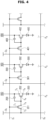
- FIG. 4 is a view illustrating an equivalent circuit of a light emitting diode panel included in a display apparatus according to an embodiment.
- the display apparatus 100 may include a data driver 104a, a scan driver 104b, and the light emitting diode panel 103.
- the light emitting diode panel 103 may include the plurality of pixels P, and each of the plurality of pixels P may include the red subpixel P R , the green subpixel P G , and the blue subpixel P B .
- the plurality of subpixels P R , P G , and P B may be arranged in two-dimensions on the light emitting diode panel 103.
- the plurality of subpixels P R , P G , and P B may be arranged in a matrix on the light emitting diode panel 103.
- the plurality of subpixels P R , P G , and P B may be arranged in rows and columns.
- a plurality of data lines D 1 , D 2 and D 3 and a plurality of scan lines S 1 and S 2 may be provided between the plurality of subpixels P R , P G , and P B .
- the plurality of scan lines S 1 and S 2 may be connected to the scan driver 104b, and the plurality of data lines D 1 , D 2 and D 3 may be connected to the data driver 104a.
- the data driver 104a may receive red/green/blue image data (hereinafter referred to as "RGB image data”) and a data control signal from the control circuit of the control assembly 106, and may output the RGB image data to the light emitting diode panel 103 according to the data control signal. Particularly, the data driver 104a may receive digital RGB image data, convert the digital RGB image data to an analog RGB image signal, and output the analog RGB image signal to the light emitting diode panel 103.
- RGB image data red/green/blue image data
- Each of a plurality of outputs provided in the data driver 104a may be connected to the plurality of data lines D 1 , D 2 , and D 3 of the light emitting diode panel 103.
- the data driver 104a may output the RGB image signal to each of the plurality of subpixels P R , P G , and P B through the plurality of data lines D 1 , D 2 , and D 3 .
- the data driver 104a may simultaneously output the RGB image signal to each of the plurality of subpixels P R , P G , and P B included in one row on the light emitting diode panel 103.
- the scan driver 104b may receive a scan control signal from the control circuit of the control assembly 106, and may activate the plurality of subpixels P R , P G , and P B included in any one of the plurality of rows according to the scan control signal. For example, the scan driver 104b may output an activation signal to any one of the plurality of scan lines S 1 and S 2 according to the scan control signal.
- the scan driver 104b may select any one of the plurality of scan lines S 1 and S 2 so that the RGB image is provided to the subpixels P R , P G , and P B belonging to an appropriate row among the plurality of subpixels P R , P G , and P B arranged in a matrix form according to the scan control signal. Also, the data driver 104a may output the RGB image signal through the plurality of data lines D 1 , D 2 , and D 3 , and the RGB image signal output by the data driver 104a may be provided to the subpixels P R , P G , and P B belonging to the row selected by the scan driver 104b.
- the data driver 104a and the scan driver 104b may sequentially provide the RGB image signals to the plurality of subpixels P R , P G , and P B included in the light emitting diode panel 103.
- Each of the plurality of subpixels P R , P G , and P B may include scan transistors 201, 301, and 401, driving transistors 202, 302, and 402, storage capacitors 203, 303, and 403, and light emitting elements 200, 300, and 400.
- the scan transistors 201, 301, and 401 may be thin film transistors (TFT) including a control terminal (Gate) T1 and first and second input/output terminals (Source, Drain) T2 and T3.
- TFT thin film transistors
- the scan transistors 201, 301, and 401 may allow current flow between the first and second input/output terminals T2 and T3 according to the control signal input to the control terminal T1 (turn-on), or may block the current flow between the first and second input/output terminals T2 and T3 (turn-off).
- the scan transistors 201, 301, and 401 When the activation signal is received from the scan driver 104b to the control terminal T1, the scan transistors 201, 301, and 401 may be turned on.
- the scan transistors 201, 301, and 401 may receive the RGB image signals of the data lines D 1 , D 2 , and D 3 through the first input/output terminal T2 and output the RGB image signals of the data lines D 1 , D 2 , and D 3 through the second input/output terminal T3.
- the scan transistors 201, 301, and 401 may be turned off.
- the light emitting elements 200, 300, and 400 may emit light having different wavelengths (different colors) depending on the constituent material.
- the light emitting diode panel 103 may include the red light emitting element 200 emitting red light, the green light emitting element 300 emitting green light, and the blue light emitting element 400 emitting blue light.
- the red light emitting element 200, the green light emitting element 300 and the blue light emitting element 400 may be provided at positions corresponding to the red subpixel P R , the green subpixel P G , and the blue subpixel P B , respectively.
- the red light emitting element 200 may output red light having different intensities according to a red image signal (hereinafter referred to as 'R image signal') output from the data driver 104a
- the green light emitting element 300 may output green light having different intensities according to a green image signal (hereinafter, referred to as 'G image signal') output from the data driver 104a
- the blue light emitting element 400 may output blue light having different intensities according to a blue image signal (hereinafter, referred to as 'B image signal') output from the data driver 104a.
- the light emitting elements 200, 300, and 400 may include the micro light emitting diodes each having the size of 100 um * 100 um or less.
- the display apparatus 100 may include the light emitting diode panel 103 having the red light emitting element 200, the green light emitting element 300, and the blue light emitting element 400.
- the red light emitting element 200, the green light emitting element 300 and the blue light emitting element 400 may have various structures to emit red light, green light, and blue light, respectively.
- the structures of the red light emitting element 200, the green light emitting element 300 and the blue light emitting element 400 may be described.
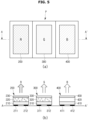
- FIG. 5 is a view illustrating an example of light emitting elements included in a display apparatus according to an embodiment.
- FIG. 6 is a view illustrating a structure of a red light emitting element included in the display apparatus illustrated in FIG. 5 and a spectrum of light output from the red light emitting element.
- FIG. 7 is a view illustrating a structure of a green light emitting element included in the display apparatus illustrated in FIG. 5 and a spectrum of light output from the green light emitting element.
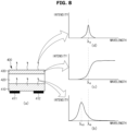
- FIG. 8 is a view illustrating a structure of a blue light emitting element included in the display apparatus illustrated in FIG. 5 and a spectrum of light output from the blue light emitting element.
- FIG. 5A illustrates one pixel included in the display apparatus 100
- FIG. 5B illustrates cross section A-A' illustrated in FIG. 5A .
- the pixels P may include the red subpixel P R , the green subpixel P G , and the blue subpixel P B .
- the red subpixel P R , the green subpixel P G , and the blue subpixel P B may be arranged side by side.
- the red subpixel P R may include the red light emitting element 200
- the green subpixel P G may include the green light emitting element 300
- the blue subpixel P B may include the blue light emitting element 400.
- the red light emitting element 200 may include a first light emitting diode 210, a red light conversion layer 220, and a red filter 230.
- the first light emitting diode 210 may include a cathode terminal 211 and an anode terminal 212, and may be connected to a driving circuit through the cathode terminal 211 and the anode terminal 212.
- the driving circuit may include the scan transistors 201, 301, and 401, the driving transistors 202, 302, and 402, and the storage capacitors 203, 303, and 403 as illustrated in FIG. 4 above.
- the first light emitting diode 210 may receive the driving current from the driving circuit through the cathode terminal 211 and the anode terminal 212 and emit light.
- the first light emitting diode 210 may emit the light having a maximum intensity at a wavelength ⁇ B1 similar to a blue wavelength (hereinafter referred to as 'light having the wavelength similar to the blue wavelength').
- the red light conversion layer 220 may absorb light emitted from the first light emitting diode 210, and may emit light having a maximum intensity at a red wavelength ⁇ R (hereinafter referred to as 'light having the red wavelength'). In other words, the red light conversion layer 220 may convert light having the wavelength ⁇ B1 similar to the blue wavelength to light having the red wavelength ⁇ R.
- the red light conversion layer 220 may include quantum dots for changing the wavelength of incident light.
- the quantum dots may refer to small sphere-shaped semiconductor particles a size of a nanometer (nm, 1,000,000,000ths of a meter), and may have a size of approximately 2 nm to 10 nm.
- the quantum dots may be composed of a core composed of cadmium selenite (CdSe), cadmium telluride (CdTe), cadmium sulfide (CdS), or the like, and a shell composed of zinc sulfide (ZnS).
- the quantum dots may have different optical characteristics than bulk materials of the same material.
- the quantum dots may emit light when a voltage is applied, or emit light of a specific wavelength when light is incident.
- the quantum dots may output light having a wavelength different from that of the incident light.
- the wavelength of the light output by the quantum dots may vary depending on the size of the quantum dots.
- An energy band gap between a valence band and a conduction band may vary depending on the size of the quantum dots, and the wavelength of light emitted from the quantum dots may vary depending on the size of the quantum dots.
- the energy band gap may be increased by a quantum confinement effect.
- the wavelength of light emitted from the quantum dots may be shortened (a frequency of light emitted from the quantum dots may be increased).
- the cadmium selenite (CdSe) bulk may emit the red light, but the cadmium selenite (CdSe) quantum dots may emit yellow light, the green light, and the blue light as its size decreases.
- the quantum dots may emit light of different wavelengths (different colors) depending on the size.
- the quantum dots with a diameter of approximately 2.5 nm may emit approximately blue light
- the quantum dots with a diameter of approximately 4 nm may emit approximately green light
- the quantum dots with a diameter of approximately 7 nm may emit approximately red light.
- the red light conversion layer 220 may include the quantum dots capable of emitting the red light.
- the red light conversion layer 220 may include the quantum dots having the diameter of approximately 7 nm.
- the red light conversion layer 220 may include a red fluorescent material that converts light having the wavelength ⁇ B1 similar to the blue wavelength to light having the red wavelength ⁇ R.
- the light emitted from the red light conversion layer 220 may include light emitted from the first light emitting diode 210 and passing through the red light conversion layer 220 (light having the wavelength similar to the blue red wavelength), and light whose wavelength is converted by the red light conversion layer 220 (light having the blue wavelength).
- the red filter 230 may pass light having the red wavelength ⁇ R among the incident light, and may block light having a wavelength different from the red light. Particularly, the red filter 230 may pass light having the red wavelength ⁇ R and block light having the wavelength ⁇ B1 similar to the blue wavelength.
- the red filter 230 is not limited to an optical filter that passes light having the red wavelength ⁇ R.
- the red filter 230 may include the optical filter that blocks light (e.g., blue light) having the wavelength shorter than the red wavelength ⁇ R and passes light having the wavelength longer than the red wavelength ⁇ R.
- a part of the light (light of the color similar to blue) emitted from the first light emitting diode 210 included in the red light emitting element 200 may be changed to red light while passing through the red light conversion layer 220, and the other part of the light emitted from the first light emitting diode 210 (light of the color similar to blue) may be blocked by the red filter 230.
- the red light emitting element 200 may emit light having the maximum intensity at the red wavelength ⁇ R.
- the wavelength deviation of the red light emitted from the red light emitting element 200 may be very small (may be approximately 2 nm or less).
- the blue light emitted from the first light emitting diode 210 may be converted into red light by the red light conversion layer 220, and the wavelength of light emitted from the red light conversion layer 220 may depend on the size of the quantum dots.
- the size of the red quantum dots may be adjusted very precisely, and the variation in size between the quantum dots is very small. Therefore, the wavelength deviation of the light emitted from the red light conversion layer 220 may also be very small.
- the green light emitting element 300 may include a second light emitting diode 310, a green light conversion layer 320, and a green filter 330.
- the second light emitting diode 310 may receive the driving current from the driving circuit through a cathode terminal 311 and an anode terminal 312. For example, as illustrated in FIG. 7B , the second light emitting diode 310 may emit light having the wavelength ⁇ B1 similar to the blue wavelength.
- the green light conversion layer 320 may absorb light (light having the wavelength similar to the blue wavelength) emitted from the second light emitting diode 310, and may emit light having the maximum intensity at a green wavelength ⁇ G (hereinafter referred to as 'light having the green wavelength').
- the red light conversion layer 220 may convert light having the wavelength ⁇ B1 similar to the blue wavelength into light having the green wavelength ⁇ G.
- the green light conversion layer 320 may include the quantum dots capable of emitting the green light.
- the green light conversion layer 320 may include the quantum dots having the diameter of approximately 4 nm.
- the green light conversion layer 320 may include a green fluorescent material that converts light having the wavelength ⁇ B1 similar to the blue wavelength to light having the green wavelength ⁇ G.
- the light emitted from the green light conversion layer 320 may include light emitted from the second light emitting diode 310 and passing through the green light conversion layer 320 (light having the wavelength similar to the blue wavelength), and light whose wavelength is converted by the green light conversion layer 320 (light having the green wavelength).
- the green filter 330 may pass light having the green wavelength ⁇ G among the incident light, and may block light having a wavelength different from the green light. Particularly, the green filter 330 may pass light having the green wavelength ⁇ G whose wavelength is converted by the green light conversion layer 320, and may block light having the wavelength ⁇ B1 similar to the blue wavelength passed through the green light conversion layer 320.
- the green filter 330 is not limited to the optical filter that passes the wavelength corresponding to green light.
- the green filter 330 may include the optical filter that blocks light (e.g., blue light) having the wavelength shorter than the green wavelength ⁇ G and passes light having the wavelength longer than the green wavelength ⁇ G.
- a part of the light of the color similar to blue emitted from the second light emitting diode 310 included in the green light emitting element 300 may be changed to green light while passing through the green light conversion layer 320, and the other part of the light may be blocked by the green filter 330.
- the green light emitting element 300 may emit light having the maximum intensity at the green wavelength ⁇ G.
- the wavelength deviation of the green light emitted from the green light emitting element 300 may be very small (may be approximately 2 nm or less). This is because the size of the green quantum dots may be adjusted very precisely, and the variation in the size between the quantum dots is very small.
- the blue light emitting element 400 may include a third light emitting diode 410, a transparent resin layer 420, and a blue filter 430.
- the third light emitting diode 410 may receive the driving current from the driving circuit through a cathode terminal 411 and an anode terminal 412. For example, as illustrated in FIG. 8B , the third light emitting diode 410 may emit light having the wavelength ⁇ B1 similar to the blue wavelength.
- the transparent resin layer 420 may pass light emitted from the third light emitting diode 410 (light having the wavelength similar to the blue wavelength).
- the transparent resin layer 420 may be composed of various transparent resins such as PC (Polycarbonate), PES (Polyether Sulfone), PMMA (Polymethyl Methacrylate), PVA (Polyvinyl alcohol), and PI (Polyimide).
- the blue filter 430 may pass light having the blue wavelength ⁇ B among the incident light and block light having a wavelength different from the blue light. Particularly, the blue filter 430 may pass light having the blue wavelength ⁇ B among light emitted from the third light emitting diode 410 and block light having the wavelength ⁇ B1 similar to the blue wavelength.
- the blue filter 430 may reduce the wavelength deviation of the light (light having the wavelength similar to the blue wavelength) emitted from the third light emitting diode 410.
- the wavelength deviation of the light emitted from the third light emitting diode 410 may be relatively large (approximately 10 nm or more).
- a mixed semiconductor such as gallium arsenide (GaAs), indium gallium nitride (InGaN), and gallium nitride (GaN) may be used.
- the light emitting diode may be manufactured by growing a first epitaxial layer containing a first impurity on a substrate and then growing a second epitaxial layer containing a second impurity. The light may be emitted at a boundary (PN junction) between the first epitaxial layer including the first impurity and the second epitaxial layer including the second impurity.
- the wavelength of the light emitted from the light emitting diode may be changed according to a mixing ratio of base materials Ga, As, In, N, etc., a concentration of the first impurity contained in the first epitaxial layer and/or a concentration of the second impurity contained in the second epitaxial layer. It is known that the blue light emitting diode has the wavelength deviation of approximately 10 nm or more due to a variation in the concentration of the first impurity and/or a variation in the concentration of the second impurity.
- the light emitted from the third light emitting diode 410 (light having the wavelength similar to the blue wavelength) has the wavelength deviation of approximately 10 nm or more, and thus, the color gamut of the display apparatus 100 may be reduced after correction of the wavelength deviation to increase display color uniformity.
- the third light emitting diode 410 outputs light having a maximum intensity at a wavelength (approximately 440 nm to 450 nm) shorter than the blue wavelength (approximately 465 nm).
- the blue filter 430 blocks light having a wavelength shorter than the blue wavelength (approximately 465 nm).
- the light passing through the blue filter 430 may have the maximum intensity at approximately the blue wavelength (approximately 465 nm).
- the wavelength deviation of the light passing through the blue filter 430 may be reduced to approximately 2 nm or less. In other words, the wavelength deviation of the blue light emitted from the blue light emitting element 400 may be approximately 2 nm or less.
- FIGS. 9 and 10 are views illustrating a wavelength deviation of light output from a blue light emitting diode included in the display apparatus illustrated in FIG. 5 .
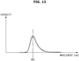
- FIGS. 11 , 12 , and 13 are views illustrating a wavelength deviation of light output from a blue light emitting element included in the display apparatus illustrated in FIG. 5 .
- a plurality of blue light emitting diodes 410-1, 410-2, 410-3, ..., and 410-n may be manufactured on a single wafer W.
- the blue light emitting diodes 410-1, 410-2, 410-3, ..., and 410-n may be composed of gallium nitride (GaN), and may emit light having the maximum intensity at the wavelength similar to the blue wavelength.
- GaN gallium nitride
- a PN junction may be formed by growing the first epitaxial layer containing the first impurity on the wafer W forming the substrate and then growing the second epitaxial layer containing the second impurity.
- a PN junction diode may be manufactured by cutting the wafer W on which the PN junction is formed to a predetermined size, and the PN junction diode may become the blue light emitting diode capable of emitting the light.
- the mixing ratio of the base materials Ga and N, the concentration of the first impurity contained in the substrate and/or the concentration of the second impurity contained in the second epitaxial layer may be different from each other.
- the wavelength of light emitted from the light emitting diode may change according to the mixing ratio of the base materials Ga and N, the concentration of the first impurity contained in the first epitaxial layer and/or the concentration of the second impurity contained in the second epitaxial layer.
- the blue light emitting diodes 410-1, 410-2, 410-3, ..., and 410-n manufactured on the single wafer W may emit light of different wavelengths.
- the wavelength deviation of the light emitted from the blue light emitting diodes 410-1, 410-2, 410-3, ..., and 410-n manufactured on the single wafer W may be generated. It is known that the wavelength deviation between the blue light emitting diodes 410-1, 410-2, 410-3, ..., and 410-n is approximately 10 nm.
- the deviation between the wavelengths ⁇ 1, ⁇ 2, ⁇ 3, ..., and ⁇ n of light emitted from the first to n-th blue light emitting diodes 410-1, 410-2, 410-3, ..., and 410-n may be approximately 10 nm.
- the first to n-th blue light-emitting diodes 410-1, 410-2, 410-3, ..., and 410-n may emit light having the wavelength of 440 nm to 450 nm.
- the plurality of blue light emitting diodes 410-1, 410-2, 410-3, ..., and 410-n manufactured by the single wafer W may emit light having the wavelength similar to blue, and the deviation may exist between the wavelengths of light emitted from the plurality of blue light emitting diodes 410-1, 410-2, 410-3, ..., and 410-n.
- the light emitted from the plurality of blue light emitting diodes 410-1, 410-2, 410-3, ..., and 410-n may have any wavelength of 440 nm to 450 nm.
- the display apparatus 100 may include the plurality of blue light emitting elements 400, and the plurality of blue light emitting elements 400 may include the plurality of blue light emitting diodes 410-1, 410-2, 410-3, ..., and 410-n and a plurality of the blue filters 430, respectively.
- the blue filter 430 may pass light having approximately the blue wavelength or light having the wavelength longer than approximately the blue wavelength ⁇ B, and may block light having the wavelength shorter than approximately the blue wavelength ⁇ B.
- the blue filter 430 may have a characteristic curve as illustrated in FIG. 11 .
- the blue filter 430 has a transmittance of about 20% at approximately 462 nm, a transmittance of about 40% at approximately 466 nm, a transmittance of about 60% at approximately 470 nm, and a transmittance of about 80% at approximately 474 nm.
- the characteristic curve of the blue filter 430 crosses the spectral curve of the blue light emitting diodes 410-1, 410-2, 410-3, ..., and 410-n at the wavelength of approximately 465 nm.
- the light passing through the blue filter 430 may have the maximum intensity at approximately 465 nm, as illustrated in FIG. 12 . Further, the wavelength deviation having the maximum intensity of the light passing through the blue filter 430 may be reduced to approximately 2 nm.
- each of the plurality of blue light emitting diodes 410-1, 410-2, 410-3, ..., and 410-n may emit light having the maximum intensity at the wavelength (approximately 440 nm to 450 nm) shorter than the blue wavelength.
- the blue filter 430 may block light having the wavelength shorter than the blue wavelength (approximately 465 nm) and pass light having the wavelength longer than the blue wavelength (approximately 465 nm), and the transmittance may be rapidly increased at the blue wavelength (approximately 465 nm).
- the wavelength deviation of the light passing through the blue filter 430 may be significantly reduced compared to the wavelength deviation of the light emitted from the plurality of blue light emitting diodes 410-1, 410-2, 410-3, ..., and 410-n.
- the wavelength deviation of the light emitted from the plurality of blue light emitting elements 400 may be significantly reduced compared to the wavelength deviation of the light emitted from the plurality of blue light emitting diodes 410-1, 410-2, 410-3, ..., and 410-n.
- a luminance correction process may be performed to reduce luminance deviation of light emitted from the plurality of blue light emitting elements 400.
- the driving current may be supplied to the blue light emitting element 400, and the luminance of the blue light emitting element 400 may be measured using a separately provided luminance meter (not shown).
- the driving current supplied to the blue light emitting element 400 may be controlled so that the luminance of the blue light emitting element 400 measured by the luminance meter has a predetermined luminance value.
- each of the plurality of pixels P may further include a compensation circuit to compensate the driving current supplied to the blue light emitting element 400 together with the driving circuit that supplies the driving current to the blue light emitting element 400.
- the plurality of blue light emitting elements 400 may emit light having a predetermined luminance value as illustrated in FIG. 13 . As a result, the luminance deviation of the light emitted from the plurality of blue light emitting elements 400 may be reduced.
- the blue light emitting element may include the blue light emitting diode and the blue filter.
- the blue light emitting diode may emit light having the wavelength shorter than the blue wavelength
- the blue filter may block light having the wavelength shorter than the blue wavelength.
- the red light emitting element may include the blue light emitting diode and the red light conversion layer.
- the red light conversion layer may absorb light emitted from the blue light emitting diode and emit light having the red wavelength.
- the wavelength deviation of the red light emitted from the red light conversion layer may be reduced compared to the wavelength deviation of the light emitted from the blue light emitting diode.
- the green light emitting element may include the blue light emitting diode and the green light conversion layer.
- the green light conversion layer may absorb light emitted from the blue light emitting diode and emit light having the green wavelength.
- the wavelength deviation of the green light emitted from the green light conversion layer may be reduced compared to the wavelength deviation of the light emitted from the blue light emitting diode.
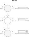
- FIG. 14 is a view illustrating a process of manufacturing a blue light emitting element included in the display apparatus illustrated in FIG. 5 .
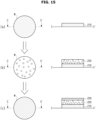
- FIG. 15 is a view illustrating a process of manufacturing a red light emitting element included in the display apparatus illustrated in FIG. 5 .
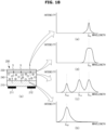
- FIG. 16 is a view illustrating a process of manufacturing a green light emitting element included in the display apparatus illustrated in FIG. 5 .
- the blue light emitting element 400 may include the blue light emitting diode, the transparent resin layer, and the blue filter.
- the wafer W may be provided, and the plurality of light emitting diodes may be formed on the wafer W.
- a plurality of the PN junctions may be formed by growing the first epitaxial layer containing the first impurity on the wafer W forming the substrate and then growing the second epitaxial layer containing the second impurity.
- Each of the plurality of PN junctions may be the light emitting diode.
- the transparent resin layer 420 may be formed on the wafer W on which the plurality of light emitting diodes are formed.
- the transparent resin layer 420 may be formed by applying (or coating) a liquid transparent resin onto the wafer W and curing the liquid transparent resin.
- the transparent resin layer 420 may be formed of various transparent resins such as PC, PES, PMMA, PVA, and PI.
- the blue filter 430 may be formed on the wafer W on which the transparent resin layer 420 is formed.
- the blue filter 430 may be formed by applying (or coating) a liquid blue pigment on the transparent resin layer 420 and curing the liquid blue pigment.
- the blue light emitting element 400 may be manufactured by cutting the wafer W on which the transparent resin layer 420 and the blue filter 430 are formed to an appropriate size.
- the wafer W may be provided, and the plurality of light emitting diodes may be formed on the wafer W.
- the wafer W on which the plurality of light emitting diodes are formed may be the same as the wafer W illustrated in FIG. 14A .
- the red light conversion layer 220 may be formed on the wafer W on which the plurality of blue light emitting diodes are formed.
- the red light conversion layer 220 may be formed by applying (or coat) a material on which the quantum dots having the diameter of approximately 7 nm and the liquid transparent resin are mixed on the wafer W and curing the material on which the quantum dots and the transparent resin are mixed.
- the red filter 230 may be formed on the wafer W on which the red light conversion layer 220 is formed, as illustrated in FIG. 15C .
- the red filter 230 may be formed by applying (or coating) a liquid red pigment on the red light conversion layer 220 and curing the liquid red pigment.
- the green light emitting element 300 may include the blue light emitting diode, the green light conversion layer, and the green filter.
- the wafer W may be provided, and the plurality of light emitting diodes may be formed on the wafer W.
- the wafer W on which the plurality of light emitting diodes are formed may be the same as the wafer W illustrated in FIG. 14A .
- the green light conversion layer 320 may be formed on the wafer W on which the plurality of blue light emitting diodes are formed.
- the green light conversion layer 320 may be formed by applying (or coat) a material on which the quantum dots having the diameter of approximately 4 nm and the liquid transparent resin are mixed on the wafer W and curing the material on which the quantum dots and the transparent resin are mixed.
- the green filter 330 may be formed on the wafer W on which the green light conversion layer 320 is formed, as illustrated in FIG. 16C .
- the green filter 330 may be formed by applying (or coating) a liquid green pigment on the green light conversion layer 320 and curing the liquid green pigment.
- the pixel P may include the red light emitting element 200, the green light emitting element 300, and the blue light emitting element 400.
- the red light emitting element 200 may include the first light emitting diode 210, a first yellow light conversion layer 240, and the red filter 230.
- the first yellow light conversion layer 240 may absorb light having the wavelength ⁇ B1 shorter than the blue wavelength emitted from the second light emitting diode 310, and may emit light having the maximum intensity at the red wavelength ⁇ R (light having the red wavelength) and light having the maximum intensity at the green wavelength ⁇ G (light having the green wavelength). In other words, the first yellow light conversion layer 240 may convert light having the wavelength ⁇ B1 shorter than the blue wavelength to light having the red wavelength ⁇ R and light having the green wavelength ⁇ G.
- the first yellow light conversion layer 240 may include a fluorescent material capable of emitting the red light and a fluorescent material capable of emitting the green light.
- the light emitted from the first yellow light conversion layer 240 may include the light having the wavelength ⁇ B1 shorter than the blue wavelength that has passed through the first yellow light conversion layer 240, and the light having the red wavelength ⁇ R whose wavelength is converted by the first yellow light conversion layer 240 and light having the green wavelength ⁇ G.
- the red filter 230 may pass light having the red wavelength ⁇ R among the incident light and block light having a wavelength different from the red wavelength ⁇ R. Particularly, the red filter 230 may pass light having the red wavelength ⁇ R and block light having the wavelength ⁇ B1 shorter than the blue wavelength and light having the green wavelength ⁇ G.
- the red light emitting element 200 may emit light having the maximum intensity at the red wavelength ⁇ R.
- the wavelength deviation of the light emitted from the first light emitting diode 210 may be reduced by the first yellow light conversion layer 240.
- the second light emitting diode 310 and the second yellow light conversion layer 340 may be the same as the first light emitting diode 210 and the first yellow light conversion layer 240 illustrated in FIG. 18 .
- the second light emitting diode 310 may emit light having the wavelength ⁇ B1 shorter than the blue wavelength, as illustrated in FIG. 19B .
- the second yellow light conversion layer 340 may convert the wavelength ⁇ B1 shorter than the blue wavelength to light having the red wavelength ⁇ R and light having the green wavelength ⁇ G.
- the second yellow light conversion layer 340 may emit light having the wavelength ⁇ B1 shorter than the blue wavelength, light having the red wavelength ⁇ R, and light having the green wavelength ⁇ G.
- the green light emitting element 300 may emit light having the maximum intensity at the green wavelength ⁇ G.
- the wavelength deviation emitted from the second light emitting diode 310 may be reduced by the second yellow light conversion layer 340.
- the third light emitting diode 410 and the third yellow light conversion layer 440 may be the same as the first light emitting diode 210 and the first yellow light conversion layer 240 illustrated in FIG. 18 .
- the third light emitting diode 410 may emit light having the wavelength ⁇ B1 shorter than the blue wavelength, as illustrated in FIG. 20B .
- the third yellow light conversion layer 440 may convert the wavelength ⁇ B1 shorter than the blue wavelength to light having the red wavelength ⁇ R and light having the green wavelength ⁇ G.
- the third yellow light conversion layer 440 may emit light having the wavelength ⁇ B1 shorter than the blue wavelength, light having the red wavelength ⁇ R, and light having the green wavelength ⁇ G.
- the blue filter 430 may pass light having the blue wavelength ⁇ B among the incident light and may block light having the wavelength different from the blue light. Particularly, the blue filter 430 may pass light having the blue wavelength ⁇ B, and may block light having the red wavelength ⁇ R and light having the green wavelength ⁇ G.
- the third light emitting diode 410 may emit light having the wavelength ⁇ B1 shorter than the blue wavelength ⁇ B, and the blue filter 430 may block light having the wavelength shorter than the blue wavelength ⁇ B, and may pass light having the wavelength longer than the blue wavelength ⁇ B.
- the blue light emitting element 400 may emit light having the maximum intensity at the blue wavelength ⁇ B.
- the wavelength deviation emitted from the third light emitting diode 410 may be reduced by the blue filter 430.
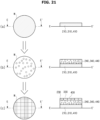
- FIG. 21 is a view illustrating a process of manufacturing a red light emitting element, a green light emitting element and a blue light emitting element illustrated in FIG. 17 .
- the wafer W may be provided, and the plurality of blue light emitting diodes may be formed on the wafer W.
- the plurality of PN junctions may be formed by growing the first epitaxial layer containing the first impurity on the wafer W forming the substrate and then growing the second epitaxial layer containing the second impurity.
- Each of the plurality of PN junctions may be the blue light emitting diode.
- the yellow light conversion layers 240, 340, and 440 may be formed on the wafer W on which the plurality of blue light emitting diodes are formed.
- the red light conversion layer 220 may apply (or coat) the material on which the quantum dots having the diameter of approximately 7 nm, the quantum dots having the diameter of approximately 4 nm and the liquid transparent resin are mixed on the wafer W, and may be formed by curing the material in which the quantum dots and the transparent resin are mixed.
- the color filters 230, 330, and 430 may be formed on the wafer W on which the yellow light conversion layers 240, 340, and 440 are formed.
- the color filters 230, 330, and 430 may include the red filter 230, the green filter 330, and the blue filter 430.
- the red filter 230, the green filter 330, and the blue filter 430 may be arranged side by side on the yellow light conversion layers 240, 340, and 440.
- the color filters 230, 330, and 430 may apply (or coat) the liquid red pigment, the green pigment, and the blue pigment on the yellow light conversion layers 240, 340, and 440, and may be formed by curing the liquid pigments.
- FIG. 22 is a view illustrating another example of light emitting elements included in a display apparatus according to an embodiment.
- FIG. 23 is a view illustrating a structure of a red light emitting element included in the display apparatus illustrated in FIG. 22 and a spectrum of light output from the red light emitting element.
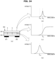
- FIG. 24 is a view illustrating a structure of a green light emitting element included in the display apparatus illustrated in FIG. 22 and a spectrum of light output from the green light emitting element.
- FIG. 25 is a view illustrating a structure of a blue light emitting element included in the display apparatus illustrated in FIG. 22 and a spectrum of light output from the blue light emitting element.
- the display apparatus 100 may include the red light emitting element 200, the green light emitting element 300, and the blue light emitting element 400.
- the red light emitting element 200 may include a red light emitting diode 250 and the red filter 230.
- the red light emitting diode 250 may be supplied with the driving current from the driving circuit through a cathode terminal 251 and an anode terminal 252.
- the red light emitting diode 250 may emit light having the maximum intensity at a wavelength ⁇ R1 similar to the red wavelength ⁇ R and shorter than the red wavelength ⁇ R.
- the red filter 230 may block light having the wavelength shorter than the red wavelength ⁇ R and pass light having the wavelength longer than the red wavelength ⁇ R. Of the light emitted from the red light emitting diode 250, the light having the wavelength longer than the red wavelength ⁇ R may pass through the red filter 230, and thus the light passing through the red filter 230 may have the maximum intensity at the red wavelength ⁇ R.
- the red light emitting element 200 may emit light having the maximum intensity at the red wavelength ⁇ R, as illustrated in FIG. 23C .
- the wavelength deviation of the light emitted from the red light emitting diode 250 may be reduced by the red filter 230.
- the green light emitting element 300 may include a green light emitting diode 350 and the green filter 330.
- the green light emitting diode 350 may be supplied with the driving current from the driving circuit through a cathode terminal 351 and an anode terminal 352.
- the green light emitting diode 350 may emit light having the maximum intensity at the wavelength ⁇ G1 similar to the green wavelength ⁇ G and shorter than the green wavelength ⁇ G.
- the green filter 330 may block light having the wavelength shorter than the green wavelength ⁇ G and pass light having the wavelength longer than the green wavelength ⁇ G. Of the light emitted from the green light emitting diode 350, the light having the wavelength longer than the green wavelength ⁇ G may pass through the green filter 330, and thus the light passing through the green filter 330 may have the maximum intensity at the green wavelength ⁇ G.
- the green light emitting element 300 may emit light having the maximum intensity at the green wavelength ⁇ G, as illustrated in FIG. 24C .
- the wavelength deviation of the light emitted from the green light emitting diode 350 may be reduced by the green filter 330.
- the blue light emitting element 400 may include a blue light emitting diode 450 and the blue filter 430.
- the blue light emitting diode 450 may be supplied with the driving current from the driving circuit through a cathode terminal 451 and an anode terminal 452.
- the blue light emitting diode 450 may emit light having the maximum intensity at the wavelength ⁇ B1 similar to the blue wavelength ⁇ B and shorter than the blue wavelength ⁇ B.
- the blue filter 430 may block light having the wavelength shorter than the blue wavelength ⁇ B and pass light having the wavelength longer than the blue wavelength ⁇ B.
- the light having the wavelength longer than the blue wavelength ⁇ B may pass through the blue filter 430, and thus the light passing through the blue filter 430 may have the maximum intensity at the blue wavelength ⁇ B.
- the blue light emitting element 400 may emit light having the maximum intensity at the blue wavelength ⁇ B, as illustrated in FIG. 25C .
- the wavelength deviation of the light emitted from the blue light emitting diode 450 may be reduced by the blue filter 430.
- the disclosed embodiments may be implemented in the form of a recording medium storing instructions that are executable by a computer.
- the instructions may be stored in the form of a program code, and when executed by a processor, the instructions may generate a program module to perform operations of the disclosed embodiments.
- the recording medium may be implemented as a computer-readable recording medium.
- the computer-readable recording medium may include all kinds of recording media storing commands that can be interpreted by a computer.
- the computer-readable recording medium may be ROM, RAM, a magnetic tape, a magnetic disc, flash memory, an optical data storage device, etc.
Landscapes
- Engineering & Computer Science (AREA)
- Physics & Mathematics (AREA)
- Computer Hardware Design (AREA)
- General Physics & Mathematics (AREA)
- Theoretical Computer Science (AREA)
- Control Of Indicators Other Than Cathode Ray Tubes (AREA)
- Led Device Packages (AREA)
- Devices For Indicating Variable Information By Combining Individual Elements (AREA)
Claims (13)
- Anzeigevorrichtung (100), umfassend:ein blaues Licht emittierendes Element (400), das dazu konfiguriert ist, blaues Licht mit einer Wellenlänge von 450 nm bis 495 nm zu emittieren;ein rotes Licht emittierendes Element (200), das dazu konfiguriert ist, rotes Licht mit einer Wellenlänge von 620 nm bis 750 nm zu emittieren, undein grünes Licht emittierendes Element (300), das dazu konfiguriert ist, grünes Licht mit einer Wellenlänge von 495 nm bis 570 nm zu emittieren,wobei das blaues Licht emittierende Element (400) Folgendes umfasst:eine erste Leuchtdiode (410), die dazu konfiguriert ist, erstes Licht mit einer maximalen Intensität bei einer Wellenlänge zu emittieren, die kürzer als eine blaue Wellenlänge ist;einen Blaufilter (430), der dazu konfiguriert ist, Licht mit der blauen Wellenlänge zu übertragen,dadurch gekennzeichnet, dassdie erste Leuchtdiode (410) dazu konfiguriert ist, Licht mit der maximalen Intensität bei einem von 440 nm bis 450 nm zu emittieren, undwobei eine Blockierkennlinie des Blaufilters (430) dazu konfiguriert ist, eine Spektralkurve der ersten Leuchtdiode (410) bei 465 nm zu kreuzen.
- Anzeigevorrichtung nach Anspruch 1, wobei die erste Leuchtdiode (410) dazu konfiguriert ist, Licht mit der maximalen Intensität bei einer von 15 nm (Nanometer) bis 25 nm kleineren Wellenlänge als die blaue Wellenlänge zu emittieren.
- Anzeigevorrichtung nach Anspruch 1, wobei die erste Leuchtdiode (410) dazu konfiguriert ist, Licht mit der maximalen Intensität bei einem von 440 nm bis 450 nm zu emittieren, und
wobei die Lichtdurchlässigkeit des Blaufilters (430) dazu konfiguriert ist, bei 465 nm schnell abzunehmen. - Anzeigevorrichtung nach Anspruch 1, wobei das blaues Licht emittierende Element ferner eine transparente Harzschicht (420) umfasst, die zwischen der ersten Leuchtdiode (410) und dem Blaufilter (430) angeordnet ist und dazu konfiguriert ist, von der ersten Leuchtdiode (410) emittiertes Licht zu übertragen.
- Anzeigevorrichtung nach Anspruch 1, wobei das blaues Licht emittierende Element ferner eine erste, zwischen der ersten Leuchtdiode (410) und dem Blaufilter (430) angeordnete Gelblichtkonversionsschicht (440) umfasst, dazu konfiguriert ist, von der ersten Leuchtdiode (410) emittiertes Licht zu absorbieren und Licht mit der Wellenlänge, die kürzer als die blaue Wellenlänge ist, Licht mit einer roten Wellenlänge und Licht mit einer grünen Wellenlänge zu emittieren.
- Anzeigevorrichtung nach Anspruch 1, ferner umfassend:eine Ansteuerungsschaltung, die dazu konfiguriert ist, dem blaues Licht emittierenden Element (400) einen Ansteuerungsstrom zuzuführen; undeine Kompensationsschaltung, die dazu konfiguriert ist, eine Leuchtdichte des Lichts zu kompensieren, das von dem blaues Licht emittierenden Element (400) emittiert wird.
- Anzeigevorrichtung nach Anspruch 6,wobei die Kompensationsschaltung dazu konfiguriert ist,den Ansteuerstrom so zu steuern, dass Licht einer vorbestimmten Leuchtdichte von dem blaues Licht emittierenden Element (400) emittiert wird.
- Anzeigevorrichtung nach Anspruch 1, wobei das rotes Licht emittierende Element (200) Folgendes umfasst:eine zweite Leuchtdiode (210), die dazu konfiguriert ist, Licht mit der maximalen Intensität bei der Wellenlänge zu emittieren, die kürzer als die blaue Wellenlänge ist; undeine Materialschicht aus roten Quantenpunkten, die dazu konfiguriert ist, von der zweiten Leuchtdiode (210) emittiertes Licht zu absorbieren und Licht mit einer roten Wellenlänge zu emittieren.
- Anzeigevorrichtung nach Anspruch 1, wobei das rotes Licht emittierende Element (200) Folgendes umfasst:eine zweite Leuchtdiode (210), die dazu konfiguriert ist, Licht mit der maximalen Intensität bei der Wellenlänge zu emittieren, die kürzer als die blaue Wellenlänge ist;eine zweite Gelblichtkonversionsschicht (240), die dazu konfiguriert ist, von der zweiten Leuchtdiode emittiertes Licht zu absorbieren und Licht mit der Wellenlänge, die kürzer als die blaue Wellenlänge ist, Licht mit einer roten Wellenlänge und Licht mit einer grünen Wellenlänge zu emittieren; undeinen Rotfilter (230), der dazu konfiguriert ist, Licht mit der roten Wellenlänge durchzulassen.
- Anzeigevorrichtung nach Anspruch 1, wobei das rotes Licht emittierende Element (200) Folgendes umfasst:eine zweite Leuchtdiode (210), die dazu konfiguriert ist, Licht mit der maximalen Intensität bei der Wellenlänge zu emittieren, die kürzer als eine rote Wellenlänge ist; undeinen Rotfilter (230), der dazu konfiguriert ist, Licht mit der Wellenlänge zu blockieren, die kürzer als die rote Wellenlänge ist.
- Anzeigevorrichtung nach Anspruch 1, wobei das grünes Licht emittierende Element (300) Folgendes umfasst:eine dritte Leuchtdiode (310), die dazu konfiguriert ist, Licht mit der maximalen Intensität bei der Wellenlänge zu emittieren, die kürzer als die blaue Wellenlänge ist; undeine Materialschicht aus grünen Quantenpunkten, die dazu konfiguriert ist, von der dritten Leuchtdiode emittiertes Licht zu absorbieren und Licht mit einer grünen Wellenlänge zu emittieren.
- Anzeigevorrichtung nach Anspruch 1, wobei das grünes Licht emittierende Element (300) Folgendes umfasst:eine dritte Leuchtdiode (310), die dazu konfiguriert ist, Licht mit der maximalen Intensität bei der Wellenlänge zu emittieren, die kürzer als die blaue Wellenlänge ist;eine dritte Gelblichtkonversionsschicht (340), die dazu konfiguriert ist, von der dritten Leuchtdiode emittiertes Licht zu absorbieren und Licht mit der Wellenlänge, die kürzer als die blaue Wellenlänge ist, Licht mit einer roten Wellenlänge und Licht mit einer grünen Wellenlänge zu emittieren; undeinen Grünfilter (330), der dazu konfiguriert ist, Licht mit der grünen Wellenlänge durchzulassen.
- Anzeigevorrichtung nach Anspruch 1, wobei das grünes Licht emittierende Element (300) Folgendes umfasst:eine zweite Leuchtdiode (310), die dazu konfiguriert ist, Licht mit der maximalen Intensität bei einer Wellenlänge zu emittieren, die kürzer als eine grüne Wellenlänge ist; undeinen Grünfilter (330), der dazu konfiguriert ist, Licht mit der Wellenlänge zu blockieren, die kürzer als die grüne Wellenlänge ist.
Applications Claiming Priority (2)
| Application Number | Priority Date | Filing Date | Title |
|---|---|---|---|
| KR1020170174156A KR102519929B1 (ko) | 2017-12-18 | 2017-12-18 | 디스플레이 장치 |
| PCT/KR2018/015915 WO2019124883A1 (ko) | 2017-12-18 | 2018-12-14 | 디스플레이 장치 |
Publications (3)
| Publication Number | Publication Date |
|---|---|
| EP3703133A1 EP3703133A1 (de) | 2020-09-02 |
| EP3703133A4 EP3703133A4 (de) | 2020-10-07 |
| EP3703133B1 true EP3703133B1 (de) | 2025-05-21 |
Family
ID=66994140
Family Applications (1)
| Application Number | Title | Priority Date | Filing Date |
|---|---|---|---|
| EP18893087.9A Active EP3703133B1 (de) | 2017-12-18 | 2018-12-14 | Anzeigevorrichtung |
Country Status (5)
| Country | Link |
|---|---|
| US (1) | US11521955B2 (de) |
| EP (1) | EP3703133B1 (de) |
| KR (1) | KR102519929B1 (de) |
| CN (1) | CN111492486B (de) |
| WO (1) | WO2019124883A1 (de) |
Families Citing this family (13)
| Publication number | Priority date | Publication date | Assignee | Title |
|---|---|---|---|---|
| CN112242411B (zh) * | 2019-07-16 | 2024-09-03 | 群创光电股份有限公司 | 显示装置 |
| KR102735082B1 (ko) * | 2019-07-24 | 2024-11-26 | 엘지디스플레이 주식회사 | Led 표시장치 |
| US11676548B2 (en) * | 2019-08-20 | 2023-06-13 | Shenzhen Tcl New Technology Co., Ltd. | Light source unit, backlight module and display device |
| CN112953633A (zh) * | 2019-12-11 | 2021-06-11 | Oppo广东移动通信有限公司 | 电子设备的通信装置及电子设备 |
| GB2595252B (en) | 2020-05-19 | 2023-10-11 | Plessey Semiconductors Ltd | Monolithic RGB micro LED display |
| US11588078B2 (en) | 2020-07-17 | 2023-02-21 | Lextar Electronics Corporation | Light emitting device and module |
| US11574953B2 (en) * | 2020-08-31 | 2023-02-07 | A.U. Vista, Inc. | Mosaic active matrix driven light emitting diode (LED) display panel |
| KR102541836B1 (ko) | 2020-09-02 | 2023-06-09 | 삼성전자주식회사 | 디스플레이 장치 |
| JP2022060047A (ja) * | 2020-10-02 | 2022-04-14 | 伯仁 ▲呉▼ | ディスプレイパネルおよびディスプレイパネル作製方法 |
| TWI759132B (zh) * | 2021-03-11 | 2022-03-21 | 聚積科技股份有限公司 | 解耦合發光顯示設備及其解耦合驅動裝置 |
| CN114512587A (zh) * | 2022-01-27 | 2022-05-17 | 华显光电技术(惠州)有限公司 | 像素单元和显示面板 |
| WO2025089269A1 (ja) * | 2023-10-23 | 2025-05-01 | Toppanホールディングス株式会社 | 表示デバイス及びその製造方法 |
| US20250316223A1 (en) * | 2024-04-03 | 2025-10-09 | Innolux Corporation | Display device |
Family Cites Families (13)
| Publication number | Priority date | Publication date | Assignee | Title |
|---|---|---|---|---|
| SG119173A1 (en) | 1999-07-08 | 2006-02-28 | Nichia Corp | Image display apparatus and its method of operation |
| KR20100089606A (ko) * | 2009-02-04 | 2010-08-12 | 한국기계연구원 | 컬러 변환층으로 반도체 나노 양자점을 포함하는 디스플레이소자 |
| KR101822537B1 (ko) * | 2011-03-31 | 2018-01-29 | 삼성디스플레이 주식회사 | 발광 다이오드 패키지, 이의 제조 방법, 및 이를 갖는 표시 장치 |
| US9658520B2 (en) * | 2012-10-01 | 2017-05-23 | Koninklijke Philips N.V. | Wavelength converting element comprising ceramic capsule |
| US9035286B2 (en) * | 2013-02-19 | 2015-05-19 | Au Optronics Corporation | Multi-color light emitting diode and method for making same |
| JP6186851B2 (ja) * | 2013-04-26 | 2017-08-30 | 日亜化学工業株式会社 | バックライト光源ユニット及びその製造方法並びに液晶表示装置 |
| US9484504B2 (en) * | 2013-05-14 | 2016-11-01 | Apple Inc. | Micro LED with wavelength conversion layer |
| JP5878579B2 (ja) * | 2014-03-31 | 2016-03-08 | シャープ株式会社 | 表示装置及びテレビ受信装置 |
| WO2016098954A1 (ko) | 2014-12-18 | 2016-06-23 | 엘지전자 주식회사 | 유기전계발광표시장치 |
| WO2017007770A2 (en) * | 2015-07-07 | 2017-01-12 | Sxaymiq Technologies Llc | Quantum dot integration schemes |
| CN105096749B (zh) * | 2015-08-04 | 2017-07-04 | 京东方科技集团股份有限公司 | 一种显示装置及其制备方法 |
| CN109219886B (zh) | 2016-04-01 | 2023-05-05 | 首尔半导体株式会社 | 显示装置及其制造方法 |
| WO2017217703A1 (en) * | 2016-06-13 | 2017-12-21 | Seoul Semiconductor Co., Ltd | Display apparatus and manufacturing method thereof |
-
2017
- 2017-12-18 KR KR1020170174156A patent/KR102519929B1/ko active Active
-
2018
- 2018-12-14 CN CN201880081547.5A patent/CN111492486B/zh active Active
- 2018-12-14 EP EP18893087.9A patent/EP3703133B1/de active Active
- 2018-12-14 US US16/955,505 patent/US11521955B2/en active Active
- 2018-12-14 WO PCT/KR2018/015915 patent/WO2019124883A1/ko not_active Ceased
Also Published As
| Publication number | Publication date |
|---|---|
| EP3703133A1 (de) | 2020-09-02 |
| EP3703133A4 (de) | 2020-10-07 |
| KR102519929B1 (ko) | 2023-04-10 |
| KR20190072965A (ko) | 2019-06-26 |
| CN111492486B (zh) | 2025-04-01 |
| CN111492486A (zh) | 2020-08-04 |
| WO2019124883A1 (ko) | 2019-06-27 |
| US20200321322A1 (en) | 2020-10-08 |
| US11521955B2 (en) | 2022-12-06 |
Similar Documents
| Publication | Publication Date | Title |
|---|---|---|
| US11521955B2 (en) | Display apparatus | |
| US10797115B2 (en) | Display panel and display apparatus using the same | |
| EP3332404B1 (de) | Anzeigevorrichtung und herstellungsverfahren | |
| KR102758863B1 (ko) | 디스플레이 장치 및 그 광원 장치 | |
| US10068884B2 (en) | Display apparatus and manufacturing method thereof | |
| CN103235442B (zh) | 一种彩膜基板、显示面板及显示装置 | |
| CN101299325B (zh) | 驱动光源的方法以及采用该方法的背光装置 | |
| US10553654B2 (en) | Display device | |
| US12078887B2 (en) | Display apparatus and backlight unit | |
| US20170179192A1 (en) | Semiconductor Devices with Integrated Thin-Film Transistor Circuitry | |
| US20150077970A1 (en) | Light source, a method of manufacturing the same, and a backlight unit having the same | |
| US12369434B2 (en) | Backlight unit including a plurality of LEDs and associated distributed bragg reflectors | |
| KR20130043294A (ko) | Led 패키지 및 이의 제조 방법 | |
| US10330265B2 (en) | Front light source and display device comprising the front light source | |
| US20200204255A1 (en) | Mobile Terminal and Method for Receiving and Sending a Lifi Signal Thereof | |
| JP2018205525A (ja) | 表示装置および電子機器 | |
| US20180321525A1 (en) | Optical film components, backlight modules, and display devices | |
| US20210167123A1 (en) | Micro led display device | |
| KR102514878B1 (ko) | 디스플레이 장치 및 그 제조 방법 | |
| US20230387144A1 (en) | Display module, display apparatus and method for manufacturing same | |
| KR102660579B1 (ko) | 디스플레이 장치 및 그 광원 장치 | |
| KR20260011066A (ko) | 디스플레이 장치 | |
| KR20250172235A (ko) | 광원 장치 및 광원 장치의 제조 방법 |
Legal Events
| Date | Code | Title | Description |
|---|---|---|---|
| STAA | Information on the status of an ep patent application or granted ep patent |
Free format text: STATUS: THE INTERNATIONAL PUBLICATION HAS BEEN MADE |
|
| PUAI | Public reference made under article 153(3) epc to a published international application that has entered the european phase |
Free format text: ORIGINAL CODE: 0009012 |
|
| STAA | Information on the status of an ep patent application or granted ep patent |
Free format text: STATUS: REQUEST FOR EXAMINATION WAS MADE |
|
| 17P | Request for examination filed |
Effective date: 20200529 |
|
| AK | Designated contracting states |
Kind code of ref document: A1 Designated state(s): AL AT BE BG CH CY CZ DE DK EE ES FI FR GB GR HR HU IE IS IT LI LT LU LV MC MK MT NL NO PL PT RO RS SE SI SK SM TR |
|
| AX | Request for extension of the european patent |
Extension state: BA ME |
|
| A4 | Supplementary search report drawn up and despatched |
Effective date: 20200909 |
|
| RIC1 | Information provided on ipc code assigned before grant |
Ipc: H01L 27/15 20060101AFI20200903BHEP Ipc: H01L 33/58 20100101ALI20200903BHEP Ipc: H01L 33/50 20100101ALI20200903BHEP |
|
| DAV | Request for validation of the european patent (deleted) | ||
| DAX | Request for extension of the european patent (deleted) | ||
| STAA | Information on the status of an ep patent application or granted ep patent |
Free format text: STATUS: EXAMINATION IS IN PROGRESS |
|
| 17Q | First examination report despatched |
Effective date: 20220124 |
|
| REG | Reference to a national code |
Ref country code: DE Ref legal event code: R079 Free format text: PREVIOUS MAIN CLASS: H01L0027150000 Ipc: H10H0029300000 Ref document number: 602018082203 Country of ref document: DE |
|
| GRAP | Despatch of communication of intention to grant a patent |
Free format text: ORIGINAL CODE: EPIDOSNIGR1 |
|
| RIC1 | Information provided on ipc code assigned before grant |
Ipc: H10H 29/851 20250101ALI20250131BHEP Ipc: H10H 29/30 20250101AFI20250131BHEP |
|
| STAA | Information on the status of an ep patent application or granted ep patent |
Free format text: STATUS: GRANT OF PATENT IS INTENDED |
|
| GRAS | Grant fee paid |
Free format text: ORIGINAL CODE: EPIDOSNIGR3 |
|
| INTG | Intention to grant announced |
Effective date: 20250313 |
|
| GRAA | (expected) grant |
Free format text: ORIGINAL CODE: 0009210 |
|
| STAA | Information on the status of an ep patent application or granted ep patent |
Free format text: STATUS: THE PATENT HAS BEEN GRANTED |
|
| AK | Designated contracting states |
Kind code of ref document: B1 Designated state(s): AL AT BE BG CH CY CZ DE DK EE ES FI FR GB GR HR HU IE IS IT LI LT LU LV MC MK MT NL NO PL PT RO RS SE SI SK SM TR |
|
| REG | Reference to a national code |
Ref country code: GB Ref legal event code: FG4D |
|
| REG | Reference to a national code |
Ref country code: CH Ref legal event code: EP |
|
| REG | Reference to a national code |
Ref country code: DE Ref legal event code: R096 Ref document number: 602018082203 Country of ref document: DE |
|
| REG | Reference to a national code |
Ref country code: IE Ref legal event code: FG4D |
|
| REG | Reference to a national code |
Ref country code: NL Ref legal event code: MP Effective date: 20250521 |
|
| PG25 | Lapsed in a contracting state [announced via postgrant information from national office to epo] |
Ref country code: FI Free format text: LAPSE BECAUSE OF FAILURE TO SUBMIT A TRANSLATION OF THE DESCRIPTION OR TO PAY THE FEE WITHIN THE PRESCRIBED TIME-LIMIT Effective date: 20250521 Ref country code: PT Free format text: LAPSE BECAUSE OF FAILURE TO SUBMIT A TRANSLATION OF THE DESCRIPTION OR TO PAY THE FEE WITHIN THE PRESCRIBED TIME-LIMIT Effective date: 20250922 Ref country code: ES Free format text: LAPSE BECAUSE OF FAILURE TO SUBMIT A TRANSLATION OF THE DESCRIPTION OR TO PAY THE FEE WITHIN THE PRESCRIBED TIME-LIMIT Effective date: 20250521 |
|
| REG | Reference to a national code |
Ref country code: LT Ref legal event code: MG9D |
|
| PG25 | Lapsed in a contracting state [announced via postgrant information from national office to epo] |
Ref country code: NO Free format text: LAPSE BECAUSE OF FAILURE TO SUBMIT A TRANSLATION OF THE DESCRIPTION OR TO PAY THE FEE WITHIN THE PRESCRIBED TIME-LIMIT Effective date: 20250821 Ref country code: GR Free format text: LAPSE BECAUSE OF FAILURE TO SUBMIT A TRANSLATION OF THE DESCRIPTION OR TO PAY THE FEE WITHIN THE PRESCRIBED TIME-LIMIT Effective date: 20250822 |
|
| PG25 | Lapsed in a contracting state [announced via postgrant information from national office to epo] |
Ref country code: NL Free format text: LAPSE BECAUSE OF FAILURE TO SUBMIT A TRANSLATION OF THE DESCRIPTION OR TO PAY THE FEE WITHIN THE PRESCRIBED TIME-LIMIT Effective date: 20250521 Ref country code: PL Free format text: LAPSE BECAUSE OF FAILURE TO SUBMIT A TRANSLATION OF THE DESCRIPTION OR TO PAY THE FEE WITHIN THE PRESCRIBED TIME-LIMIT Effective date: 20250521 |
|
| PG25 | Lapsed in a contracting state [announced via postgrant information from national office to epo] |
Ref country code: BG Free format text: LAPSE BECAUSE OF FAILURE TO SUBMIT A TRANSLATION OF THE DESCRIPTION OR TO PAY THE FEE WITHIN THE PRESCRIBED TIME-LIMIT Effective date: 20250521 |
|
| PG25 | Lapsed in a contracting state [announced via postgrant information from national office to epo] |
Ref country code: HR Free format text: LAPSE BECAUSE OF FAILURE TO SUBMIT A TRANSLATION OF THE DESCRIPTION OR TO PAY THE FEE WITHIN THE PRESCRIBED TIME-LIMIT Effective date: 20250521 |
|
| PG25 | Lapsed in a contracting state [announced via postgrant information from national office to epo] |
Ref country code: RS Free format text: LAPSE BECAUSE OF FAILURE TO SUBMIT A TRANSLATION OF THE DESCRIPTION OR TO PAY THE FEE WITHIN THE PRESCRIBED TIME-LIMIT Effective date: 20250821 |
|
| PG25 | Lapsed in a contracting state [announced via postgrant information from national office to epo] |
Ref country code: IS Free format text: LAPSE BECAUSE OF FAILURE TO SUBMIT A TRANSLATION OF THE DESCRIPTION OR TO PAY THE FEE WITHIN THE PRESCRIBED TIME-LIMIT Effective date: 20250921 |
|
| PG25 | Lapsed in a contracting state [announced via postgrant information from national office to epo] |
Ref country code: LV Free format text: LAPSE BECAUSE OF FAILURE TO SUBMIT A TRANSLATION OF THE DESCRIPTION OR TO PAY THE FEE WITHIN THE PRESCRIBED TIME-LIMIT Effective date: 20250521 |
|
| REG | Reference to a national code |
Ref country code: AT Ref legal event code: MK05 Ref document number: 1798051 Country of ref document: AT Kind code of ref document: T Effective date: 20250521 |
|
| PGFP | Annual fee paid to national office [announced via postgrant information from national office to epo] |
Ref country code: DE Payment date: 20251120 Year of fee payment: 8 |
|
| PG25 | Lapsed in a contracting state [announced via postgrant information from national office to epo] |
Ref country code: DK Free format text: LAPSE BECAUSE OF FAILURE TO SUBMIT A TRANSLATION OF THE DESCRIPTION OR TO PAY THE FEE WITHIN THE PRESCRIBED TIME-LIMIT Effective date: 20250521 Ref country code: AT Free format text: LAPSE BECAUSE OF FAILURE TO SUBMIT A TRANSLATION OF THE DESCRIPTION OR TO PAY THE FEE WITHIN THE PRESCRIBED TIME-LIMIT Effective date: 20250521 Ref country code: SM Free format text: LAPSE BECAUSE OF FAILURE TO SUBMIT A TRANSLATION OF THE DESCRIPTION OR TO PAY THE FEE WITHIN THE PRESCRIBED TIME-LIMIT Effective date: 20250521 |
|
| PG25 | Lapsed in a contracting state [announced via postgrant information from national office to epo] |
Ref country code: CZ Free format text: LAPSE BECAUSE OF FAILURE TO SUBMIT A TRANSLATION OF THE DESCRIPTION OR TO PAY THE FEE WITHIN THE PRESCRIBED TIME-LIMIT Effective date: 20250521 |
|
| PG25 | Lapsed in a contracting state [announced via postgrant information from national office to epo] |
Ref country code: EE Free format text: LAPSE BECAUSE OF FAILURE TO SUBMIT A TRANSLATION OF THE DESCRIPTION OR TO PAY THE FEE WITHIN THE PRESCRIBED TIME-LIMIT Effective date: 20250521 |
|
| PG25 | Lapsed in a contracting state [announced via postgrant information from national office to epo] |
Ref country code: SK Free format text: LAPSE BECAUSE OF FAILURE TO SUBMIT A TRANSLATION OF THE DESCRIPTION OR TO PAY THE FEE WITHIN THE PRESCRIBED TIME-LIMIT Effective date: 20250521 Ref country code: RO Free format text: LAPSE BECAUSE OF FAILURE TO SUBMIT A TRANSLATION OF THE DESCRIPTION OR TO PAY THE FEE WITHIN THE PRESCRIBED TIME-LIMIT Effective date: 20250521 |
|
| PG25 | Lapsed in a contracting state [announced via postgrant information from national office to epo] |
Ref country code: IT Free format text: LAPSE BECAUSE OF FAILURE TO SUBMIT A TRANSLATION OF THE DESCRIPTION OR TO PAY THE FEE WITHIN THE PRESCRIBED TIME-LIMIT Effective date: 20250521 |
|
| REG | Reference to a national code |
Ref country code: DE Ref legal event code: R097 Ref document number: 602018082203 Country of ref document: DE |
|
| PLBE | No opposition filed within time limit |
Free format text: ORIGINAL CODE: 0009261 |
|
| STAA | Information on the status of an ep patent application or granted ep patent |
Free format text: STATUS: NO OPPOSITION FILED WITHIN TIME LIMIT |
|
| REG | Reference to a national code |
Ref country code: CH Ref legal event code: L10 Free format text: ST27 STATUS EVENT CODE: U-0-0-L10-L00 (AS PROVIDED BY THE NATIONAL OFFICE) Effective date: 20260402 |
|
| 26N | No opposition filed |
Effective date: 20260224 |
|
| PG25 | Lapsed in a contracting state [announced via postgrant information from national office to epo] |
Ref country code: LT Free format text: LAPSE BECAUSE OF FAILURE TO SUBMIT A TRANSLATION OF THE DESCRIPTION OR TO PAY THE FEE WITHIN THE PRESCRIBED TIME-LIMIT Effective date: 20250521 |
|
| PG25 | Lapsed in a contracting state [announced via postgrant information from national office to epo] |
Ref country code: MC Free format text: LAPSE BECAUSE OF FAILURE TO SUBMIT A TRANSLATION OF THE DESCRIPTION OR TO PAY THE FEE WITHIN THE PRESCRIBED TIME-LIMIT Effective date: 20250521 |
|
| REG | Reference to a national code |
Ref country code: CH Ref legal event code: H13 Free format text: ST27 STATUS EVENT CODE: U-0-0-H10-H13 (AS PROVIDED BY THE NATIONAL OFFICE) Effective date: 20260723 |
|
| PG25 | Lapsed in a contracting state [announced via postgrant information from national office to epo] |
Ref country code: SE Free format text: LAPSE BECAUSE OF FAILURE TO SUBMIT A TRANSLATION OF THE DESCRIPTION OR TO PAY THE FEE WITHIN THE PRESCRIBED TIME-LIMIT Effective date: 20250521 |