EP3695431B1 - Ruthenium encapsulated photocathode electron emitter - Google Patents
Ruthenium encapsulated photocathode electron emitter Download PDFInfo
- Publication number
- EP3695431B1 EP3695431B1 EP18865695.3A EP18865695A EP3695431B1 EP 3695431 B1 EP3695431 B1 EP 3695431B1 EP 18865695 A EP18865695 A EP 18865695A EP 3695431 B1 EP3695431 B1 EP 3695431B1
- Authority
- EP
- European Patent Office
- Prior art keywords
- protective film
- electron
- photocathode
- electron emitter
- ruthenium
- Prior art date
- Legal status (The legal status is an assumption and is not a legal conclusion. Google has not performed a legal analysis and makes no representation as to the accuracy of the status listed.)
- Active
Links
Images

Classifications
-
- H—ELECTRICITY
- H01—ELECTRIC ELEMENTS
- H01J—ELECTRIC DISCHARGE TUBES OR DISCHARGE LAMPS
- H01J37/00—Discharge tubes with provision for introducing objects or material to be exposed to the discharge, e.g. for the purpose of examination or processing thereof
- H01J37/02—Details
- H01J37/04—Arrangements of electrodes and associated parts for generating or controlling the discharge, e.g. electron-optical arrangement or ion-optical arrangement
- H01J37/06—Electron sources; Electron guns
- H01J37/073—Electron guns using field emission, photo emission, or secondary emission electron sources
-
- G—PHYSICS
- G02—OPTICS
- G02B—OPTICAL ELEMENTS, SYSTEMS OR APPARATUS
- G02B27/00—Optical systems or apparatus not provided for by any of the groups G02B1/00 - G02B26/00, G02B30/00
- G02B27/09—Beam shaping, e.g. changing the cross-sectional area, not otherwise provided for
- G02B27/0927—Systems for changing the beam intensity distribution, e.g. Gaussian to top-hat
-
- H—ELECTRICITY
- H01—ELECTRIC ELEMENTS
- H01J—ELECTRIC DISCHARGE TUBES OR DISCHARGE LAMPS
- H01J1/00—Details of electrodes, of magnetic control means, of screens, or of the mounting or spacing thereof, common to two or more basic types of discharge tubes or lamps
- H01J1/02—Main electrodes
- H01J1/30—Cold cathodes, e.g. field-emissive cathode
- H01J1/304—Field-emissive cathodes
- H01J1/3042—Field-emissive cathodes microengineered, e.g. Spindt-type
- H01J1/3044—Point emitters
-
- H—ELECTRICITY
- H01—ELECTRIC ELEMENTS
- H01J—ELECTRIC DISCHARGE TUBES OR DISCHARGE LAMPS
- H01J19/00—Details of vacuum tubes of the types covered by group H01J21/00
- H01J19/02—Electron-emitting electrodes; Cathodes
- H01J19/24—Cold cathodes, e.g. field-emissive cathode
-
- H—ELECTRICITY
- H01—ELECTRIC ELEMENTS
- H01J—ELECTRIC DISCHARGE TUBES OR DISCHARGE LAMPS
- H01J37/00—Discharge tubes with provision for introducing objects or material to be exposed to the discharge, e.g. for the purpose of examination or processing thereof
- H01J37/02—Details
- H01J37/04—Arrangements of electrodes and associated parts for generating or controlling the discharge, e.g. electron-optical arrangement or ion-optical arrangement
- H01J37/06—Electron sources; Electron guns
-
- H—ELECTRICITY
- H01—ELECTRIC ELEMENTS
- H01J—ELECTRIC DISCHARGE TUBES OR DISCHARGE LAMPS
- H01J37/00—Discharge tubes with provision for introducing objects or material to be exposed to the discharge, e.g. for the purpose of examination or processing thereof
- H01J37/26—Electron or ion microscopes; Electron or ion diffraction tubes
- H01J37/28—Electron or ion microscopes; Electron or ion diffraction tubes with scanning beams
-
- H—ELECTRICITY
- H01—ELECTRIC ELEMENTS
- H01J—ELECTRIC DISCHARGE TUBES OR DISCHARGE LAMPS
- H01J40/00—Photoelectric discharge tubes not involving the ionisation of a gas
- H01J40/02—Details
- H01J40/04—Electrodes
- H01J40/06—Photo-emissive cathodes
-
- H—ELECTRICITY
- H01—ELECTRIC ELEMENTS
- H01J—ELECTRIC DISCHARGE TUBES OR DISCHARGE LAMPS
- H01J40/00—Photoelectric discharge tubes not involving the ionisation of a gas
- H01J40/16—Photoelectric discharge tubes not involving the ionisation of a gas having photo- emissive cathode, e.g. alkaline photoelectric cell
- H01J40/18—Photoelectric discharge tubes not involving the ionisation of a gas having photo- emissive cathode, e.g. alkaline photoelectric cell with luminescent coatings for influencing the sensitivity of the tube, e.g. by converting the input wavelength
-
- H—ELECTRICITY
- H01—ELECTRIC ELEMENTS
- H01J—ELECTRIC DISCHARGE TUBES OR DISCHARGE LAMPS
- H01J1/00—Details of electrodes, of magnetic control means, of screens, or of the mounting or spacing thereof, common to two or more basic types of discharge tubes or lamps
- H01J1/02—Main electrodes
- H01J1/34—Photo-emissive cathodes
-
- H—ELECTRICITY
- H01—ELECTRIC ELEMENTS
- H01J—ELECTRIC DISCHARGE TUBES OR DISCHARGE LAMPS
- H01J2201/00—Electrodes common to discharge tubes
- H01J2201/30—Cold cathodes
- H01J2201/304—Field emission cathodes
- H01J2201/30403—Field emission cathodes characterised by the emitter shape
- H01J2201/30407—Microengineered point emitters
- H01J2201/30411—Microengineered point emitters conical shaped, e.g. Spindt type
-
- H—ELECTRICITY
- H01—ELECTRIC ELEMENTS
- H01J—ELECTRIC DISCHARGE TUBES OR DISCHARGE LAMPS
- H01J2201/00—Electrodes common to discharge tubes
- H01J2201/30—Cold cathodes
- H01J2201/304—Field emission cathodes
- H01J2201/30446—Field emission cathodes characterised by the emitter material
- H01J2201/30449—Metals and metal alloys
-
- H—ELECTRICITY
- H01—ELECTRIC ELEMENTS
- H01J—ELECTRIC DISCHARGE TUBES OR DISCHARGE LAMPS
- H01J2201/00—Electrodes common to discharge tubes
- H01J2201/30—Cold cathodes
- H01J2201/304—Field emission cathodes
- H01J2201/30446—Field emission cathodes characterised by the emitter material
- H01J2201/3048—Semiconductor materials
-
- H—ELECTRICITY
- H01—ELECTRIC ELEMENTS
- H01J—ELECTRIC DISCHARGE TUBES OR DISCHARGE LAMPS
- H01J2201/00—Electrodes common to discharge tubes
- H01J2201/30—Cold cathodes
- H01J2201/308—Semiconductor cathodes, e.g. having PN junction layers
-
- H—ELECTRICITY
- H01—ELECTRIC ELEMENTS
- H01J—ELECTRIC DISCHARGE TUBES OR DISCHARGE LAMPS
- H01J2201/00—Electrodes common to discharge tubes
- H01J2201/34—Photoemissive electrodes
- H01J2201/342—Cathodes
- H01J2201/3421—Composition of the emitting surface
- H01J2201/3423—Semiconductors, e.g. GaAs, NEA emitters
-
- H—ELECTRICITY
- H01—ELECTRIC ELEMENTS
- H01J—ELECTRIC DISCHARGE TUBES OR DISCHARGE LAMPS
- H01J2201/00—Electrodes common to discharge tubes
- H01J2201/34—Photoemissive electrodes
- H01J2201/342—Cathodes
- H01J2201/3421—Composition of the emitting surface
- H01J2201/3425—Metals, metal alloys
-
- H—ELECTRICITY
- H01—ELECTRIC ELEMENTS
- H01J—ELECTRIC DISCHARGE TUBES OR DISCHARGE LAMPS
- H01J2201/00—Electrodes common to discharge tubes
- H01J2201/34—Photoemissive electrodes
- H01J2201/342—Cathodes
- H01J2201/3421—Composition of the emitting surface
- H01J2201/3426—Alkaline metal compounds, e.g. Na-K-Sb
-
- H—ELECTRICITY
- H01—ELECTRIC ELEMENTS
- H01J—ELECTRIC DISCHARGE TUBES OR DISCHARGE LAMPS
- H01J2237/00—Discharge tubes exposing object to beam, e.g. for analysis treatment, etching, imaging
- H01J2237/06—Sources
- H01J2237/063—Electron sources
- H01J2237/06325—Cold-cathode sources
- H01J2237/06333—Photo emission
-
- H—ELECTRICITY
- H01—ELECTRIC ELEMENTS
- H01J—ELECTRIC DISCHARGE TUBES OR DISCHARGE LAMPS
- H01J2237/00—Discharge tubes exposing object to beam, e.g. for analysis treatment, etching, imaging
- H01J2237/245—Detection characterised by the variable being measured
- H01J2237/24507—Intensity, dose or other characteristics of particle beams or electromagnetic radiation
- H01J2237/24514—Beam diagnostics including control of the parameter or property diagnosed
- H01J2237/24521—Beam diameter
-
- H—ELECTRICITY
- H01—ELECTRIC ELEMENTS
- H01J—ELECTRIC DISCHARGE TUBES OR DISCHARGE LAMPS
- H01J2237/00—Discharge tubes exposing object to beam, e.g. for analysis treatment, etching, imaging
- H01J2237/245—Detection characterised by the variable being measured
- H01J2237/24592—Inspection and quality control of devices
-
- H—ELECTRICITY
- H01—ELECTRIC ELEMENTS
- H01J—ELECTRIC DISCHARGE TUBES OR DISCHARGE LAMPS
- H01J2237/00—Discharge tubes exposing object to beam, e.g. for analysis treatment, etching, imaging
- H01J2237/26—Electron or ion microscopes
- H01J2237/28—Scanning microscopes
- H01J2237/2813—Scanning microscopes characterised by the application
- H01J2237/2817—Pattern inspection
-
- H—ELECTRICITY
- H01—ELECTRIC ELEMENTS
- H01L—SEMICONDUCTOR DEVICES NOT COVERED BY CLASS H10
- H01L21/00—Processes or apparatus adapted for the manufacture or treatment of semiconductor or solid state devices or of parts thereof
- H01L21/67—Apparatus specially adapted for handling semiconductor or electric solid state devices during manufacture or treatment thereof; Apparatus specially adapted for handling wafers during manufacture or treatment of semiconductor or electric solid state devices or components ; Apparatus not specifically provided for elsewhere
- H01L21/67005—Apparatus not specifically provided for elsewhere
- H01L21/67242—Apparatus for monitoring, sorting or marking
- H01L21/67288—Monitoring of warpage, curvature, damage, defects or the like
Definitions
- This disclosure relates to protective films for electron emitters.
- Fabricating semiconductor devices typically includes processing a semiconductor wafer using a large number of fabrication processes to form various features and multiple levels of the semiconductor devices.
- lithography is a semiconductor fabrication process that involves transferring a pattern from a reticle to a photoresist arranged on a semiconductor wafer.
- Additional examples of semiconductor fabrication processes include, but are not limited to, chemical-mechanical polishing (CMP), etch, deposition, and ion implantation.
- CMP chemical-mechanical polishing
- etch etch
- deposition deposition
- ion implantation ion implantation
- Electron beams are used in a number of different applications during semiconductor manufacturing. For example, electron beams can be modulated and directed onto an electronsensitive resist on a semiconductor wafer, mask, or other workpiece to generate an electron pattern on the workpiece. Electron beams also can be used to inspect a wafer by, for example, detecting electrons emerging or reflected from the wafer to detect defects, anomalies, or undesirable objects.
- Inspection processes are used at various steps during a semiconductor manufacturing process to promote higher yield in the manufacturing process and, thus, higher profits. Inspection has always been an important part of fabricating semiconductor devices such as integrated circuits (ICs). However, as the dimensions of semiconductor devices decrease, inspection becomes even more important to the successful manufacture of acceptable semiconductor devices because smaller defects can cause the devices to fail. For instance, as the dimensions of semiconductor devices decrease, detection of defects of decreasing size has become necessary because even relatively small defects may cause unwanted aberrations in the semiconductor devices.
- Photocathodes also have been used to generate electron beams.
- a single light beam incident on a photocathode system can generate a single electron beam with high brightness that is capable of delivering high electron current density.
- a problem with single electron beam systems is that even with high brightness systems, single electron beam systems still have relative low throughput for inspection. Low throughput is a drawback to electron beam inspection. With currently-available electron beam sources, thousands of beams would be required.
- Alkali halide photo electron emitters are used as photocathode emitters in the ultraviolet spectral range.
- CsBr and CsI photocathodes are used for high quantum efficiency with light in the deep ultraviolet (DUV) range.
- DUV deep ultraviolet
- Photocathode electron emitters generally do not have a protective coating to protect them from oxidation or carbon build up from the vacuum environment.
- Existing protective cap layers on photocathodes are not robust to cleaning. Therefore, these cap layers cannot protect a photocathode electron emitter during operation.
- Alkali halide photocathodes such as CsI and CsBr have demonstrated photoemission from intraband states when illuminated with wavelengths much longer than their bandgap energy. So far, the illumination schemes to pump these photocathodes involve either short wavelengths with energies larger than the bandgap or longer wavelengths that first activate the color centers located at about 4.7 eV above the valence band. These schemes have been tried both in transmission and in reflection mode. For reflection mode, 257 nm and 266 nm beams have successfully activated the color centers and photogenerated electrons in vacuum. A 410 nm beam was not successful at activating defects and simultaneously transferring the electrons to vacuum.
- US2004/140432 discloses an electron beam apparatus that comprises a beam source to generate a radiation beam that is directed onto a photocathode to generate an electron beam.
- the photocathode comprises a protective layer.
- a electron emitter as recited in claim 1 is provided in a first embodiment.
- An electron beam tool including the electron emitter of the first embodiment as recited in claim 8 is provided.
- a method as recited in claim 9 is provided in a second embodiment.
- Ruthenium or a ruthenium alloy can be used to encapsulate one or more surfaces of a photocathode.
- Photocathodes are affected by vacuum conditions that can deteriorate the field emission performance.
- the photocathode can be wholly or partly encapsulated with a ruthenium protective film.
- the ruthenium protective film renders the photocathode resistant to oxidation and carbon build up.
- the ruthenium protective film also has a relative low sputter yields and can withstand erosion by ions.
- ruthenium is a metal and may have advantages over using the photocathode by itself. For example, use of ruthenium may provide higher current stability and/or operation at higher pressures.
- a protective film that can protect from oxidation and carbon build up would be beneficial.
- a protective film with ruthenium or a ruthenium alloy can provide these benefits.
- the brightness of a photocathode emitter depends primarily on the photocathode material and the excitation wavelength with a general tradeoff between quantum efficiency and emittance. Dual wavelength excitation or dual transmission/reflection excitation schemes can be used for brightness optimization.
- Photocathodes are electron sources that emit electrons when a photocathode structure is exposed to a source of light, either in transmission or reflection mode.
- the photocathode structure can be a bulk material, a film, or series of films deposited on a substrate.
- the wavelength(s) of the light can be selected to optimize the amount of emission currents and energy spread of the emitted electrons.
- the current produced by photocathodes may be more stable than the current produced by cold field emitters.
- Many materials can be used for photoemission, including silicon, silicon with a metal coating, or an alkali halide.
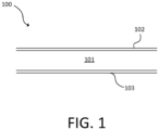
- FIG. 1 is a cross-sectional diagram of an embodiment of an electron emitter 100.
- the electron emitter 100 includes a photocathode structure 101.
- the photocathode structure 101 can include an alkali halide, such as CsBr or CsI.
- the photocathode structure 101 also can include other semiconductor photocathode materials.
- the photocathode structure 101 may include planar features.
- a protective film 102 is disposed on an exterior surface of the photocathode structure 101.
- the protective film 102 includes ruthenium.
- the protective film 102 may be ruthenium or a ruthenium alloy, such as an alloy of ruthenium and platinum.
- the electron emitter 100 can optionally include a layer 103 on a side of the photocathode structure 101 opposite from the protective film 102.
- the layer 103 may include ruthenium or may be another metal.
- Introducing voltage to the protective film 102 and/or layer 103 can provide control of electron migration to desired surface. For example, if the layer 103 on the back side of the electron emitter 100 is positively charged, electrons can be made to migrate to the exit surface to enhance electron emission.
- the protective film 102 can have a thickness from 1 nm to 20 nm or from 1 nm to 10 nm, including all values to the 0.1 nm and ranges in between. This thickness can be measured from an outer surface of the photocathode structure 101 or another layer that the protective film 102 is disposed on.
- the optimal thickness of the protective film 102 can be configured for optimal electron emission. Larger thicknesses, while feasible, may affect efficiency. The thickness may depend on the electron emitter 100 extractor configuration and wavelength used for photo electron emission. If the thickness is too large, then it will absorb all the light and/or will not allow electrons to escape easily by increasing the work function. As the protective film 102 generally provides a protective function, it can be thick enough to protect the photocathode structure 101 without affecting performance. The protective film 102 also can supply electrons, so the thickness can vary with the wavelength of light used for electron generation.
- the protective film 102 may be free of pinholes in at least an emitting area of the photocathode structure 101.
- the protective film 102 can have a porosity less than or equal to 25%. Protection may be compromised if the porosity is greater than 25%.
- the protective film 102 can have a packing density of greater than or equal to 0.92. Protection may be compromised with a packing density less than 0.92.
- the protective film 102 can be deposited by ion or magnetron sputtering, atomic layer deposition (ALD), or by other methods that provide a dense, pinhole-free, uniform protective film 102.
- n f is the refractive index of the protective film 102 and n b is the refractive index of the material.
- PD n f 2 ⁇ 1 ⁇ n b 2 + 2 n f 2 + 2 ⁇ n b 2 ⁇ 1
- the protective film 102 may be free of bubbles and inclusions in at least an emitting area.
- the protective film 102 may include imperfections only with a diameter or length dimension less than 1 nm.
- the protective film 102 may have fewer than 10 4 impurities over an emitting area.
- the impurities can include carbon, oxides, oxygen as a dissolved gas, sodium, or potassium.
- the protective film 102 can be robust for electron field emission, robust in the presence of high electric fields, robust to ion sputtering, and robust to plasma or other cleaning methods. Oxidation and/or carbon can be removed from the protective film 102 without damaging the protective film 102. For example, the protective film 102 can be cleaned to atomic levels by molecular hydrogen, hydrogen plasmas, or other plasmas.
- the protective film 102 also is resistant to oxidation and carbon contamination. Ruthenium may have the ability to break apart gas molecules that land on its surface or prevent adherence of such gas molecules to its surface. These molecules are capable of distorting the extraction field on the surface of the electron emitter 100 and causing enhanced emission which translates as noise in the beam because of the mobility and residence time of the molecule on the surface. Thus, the protective film 102 can be self-cleaning.
- the protective film 102 on the photocathode structure 101 can control electromigration to a desired surface, such as during application of a voltage. Electromigration can be controlled with the protective film 102 on one surface of the photocathode structure 101 and ruthenium or another metal on an opposite surface of the photocathode structure 101.
- the protective film 102 also may provide improved angular spread of the electron beam.
- Photocathodes generally can operate at approximately 10 -11 Torr.
- the electron emitter 100 may be able to operate at approximately 10 -9 Torr.
- the protective film 102 is transparent to UV wavelengths. This can enable operation of the electron emitter 100 in both transmission and reflection modes.
- Embodiments of the electron source 100 can be used as the electron source in reticle and wafer inspection systems.
- embodiments of the electron source 100 can be used as the electron source in electron beam wafer or reticle inspection systems using single or multiple electron sources, electron beam wafer or reticle review systems using single or multiple electron sources, or electron beam wafer or reticle metrology systems using single or multiple electron sources.
- Embodiments of the electron source 100 also can be used in systems that generate x-rays using single or multiple electron sources in wafer or reticle metrology, review, or inspection.
- Multiple wavelengths can be applied to the photocathode structure 101 that includes an alkali halide, such as CsBr or CsI.
- the multiple wavelengths can be applied in both reflection and transmission mode to activate and pump intraband states (e.g., color centers) of the alkali halide.
- the multiple wavelengths can activate the centers and transfer electrons to vacuum.
- Use of multiple wavelengths can increase quantum efficiency and/or achieve the same quantum efficiency as with a single wavelength while producing less heat.
- Less complex lasers systems can be used to generate multiple wavelengths than a single wavelength. For example, a longer wavelength can use a less complex laser system or optics. Less energy spread of the photogenerated electrons and lower emittance can be achieved.
- FIG. 2 illustrates the conduction band (CB) and valence band (VB).
- the third pumping scheme using two wavelengths may be an equivalent to electromagnetically-induced transparency (EIT) where ⁇ 1 blocks the color centers from absorbing ⁇ 3, which can enable electrons to be pumped directly from the valence band to vacuum.
- EIT electromagnetically-induced transparency
- the dual wavelength pumping scheme can minimize required optical power per photogenerated electron, which can provide higher quantum efficiency. Heat dissipation per photogenerated electron also can be minimized.
- a dual wavelength pumping scheme also can provide improve localization of induced current.
- Dual wavelength pumping schemes can be performed concurrently in transmission and reflection mode, which can optimize efficiency.
- Longer photocathode and optics lifetimes can be achieved with longer wavelength illumination, such as those using a dual wavelength pumping scheme.
- Lower emittance and energy spread also can be achieved using longer wavelengths, such as with a dual wavelength pumping scheme.
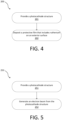
- FIG. 4 is a flowchart of a method 200.
- a photocathode structure is provided at 201.
- the photocathode structure includes an alkali halide.
- a protective film that includes ruthenium is deposited on an exterior surface of the photocathode structure at 202.
- the deposition can include ion sputtering, magnetron sputtering, or ALD. The deposition can provide the desired film density, conformal nature, and amount of pinhole defects.
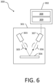
- FIG. 5 is a flowchart of a method 250.
- a photocathode structure is provided at 251.
- the photocathode structure includes an alkali halide and a protective film disposed on an exterior surface of the photocathode structure.
- the protective film includes ruthenium.
- An electron beam is generated from the photocathode structure at 252 when photons are directed at the photocathode structure. Electron generation may occur at approximately 10 -5 Torr or less.
- a plasma clean can optionally be performed on the photocathode structure after the electron beam is generated.
- the electron beam produced using the photocathode structure with the protective film can have a higher quantum efficiency than a photocathode structure without the protective film.
- FIG. 6 is a block diagram of an embodiment of a system 300.
- the system 300 includes a wafer inspection tool (which includes the electron column 301) configured to generate images of a wafer 304.
- the wafer inspection tool includes an output acquisition subsystem that includes at least an energy source and a detector.
- the output acquisition subsystem may be an electron beam-based output acquisition subsystem.
- the energy directed to the wafer 304 includes electrons
- the energy detected from the wafer 304 includes electrons.
- the energy source may be an electron beam source.
- the output acquisition subsystem includes electron column 301, which is coupled to computer subsystem 302.
- a chuck (not illustrated) may hold the wafer 304.
- the electron column 301 includes an electron beam source 303 configured to generate electrons that are focused to wafer 304 by one or more elements 305.
- the electron beam source 303 may include, for example, an embodiment of the electron source 100 of FIG. 1 .
- the one or more elements 305 may include, for example, a gun lens, an anode, a beam limiting aperture, a gate valve, a beam current selection aperture, an objective lens, and a scanning subsystem, all of which may include any such suitable elements known in the art.
- Electrons returned from the wafer 304 may be focused by one or more elements 306 to detector 307.
- One or more elements 306 may include, for example, a scanning subsystem, which may be the same scanning subsystem included in element(s) 305.
- the electron column also may include any other suitable elements known in the art.
- the electron column 301 is shown in FIG. 6 as being configured such that the electrons are directed to the wafer 304 at an oblique angle of incidence and are scattered from the wafer 304 at another oblique angle
- the electron beam may be directed to and scattered from the wafer 304 at any suitable angles.
- the electron beam-based output acquisition subsystem may be configured to use multiple modes to generate images of the wafer 304 (e.g., with different illumination angles, collection angles, etc.). The multiple modes of the electron beam-based output acquisition subsystem may be different in any image generation parameters of the output acquisition subsystem.
- Computer subsystem 302 may be coupled to detector 307 such that the computer subsystem 302 is in electronic communication with the detector 307 or other components of the wafer inspection tool.
- the detector 307 may detect electrons returned from the surface of the wafer 304 thereby forming electron beam images of the wafer 304 with the computer subsystem 302.
- the electron beam images may include any suitable electron beam images.
- the computer subsystem 302 includes a processor 308 and an electronic data storage unit 309.
- the processor 308 may include a microprocessor, a microcontroller, or other devices.
- FIG. 6 is provided herein to generally illustrate a configuration of an electron beam-based output acquisition subsystem that may be used in the embodiments described herein.
- the electron beam-based output acquisition subsystem configuration described herein may be altered to optimize the performance of the output acquisition subsystem as is normally performed when designing a commercial output acquisition system.
- the systems described herein may be implemented using an existing system (e.g., by adding functionality described herein to an existing system).
- the methods described herein may be provided as optional functionality of the system (e.g., in addition to other functionality of the system).
- the system described herein may be designed as a completely new system.
- the computer subsystem 302 may be coupled to the components of the system 300 in any suitable manner (e.g., via one or more transmission media, which may include wired and/or wireless transmission media) such that the processor 308 can receive output.
- the processor 308 may be configured to perform a number of functions using the output.
- the wafer inspection tool can receive instructions or other information from the processor 308.
- the processor 308 and/or the electronic data storage unit 309 optionally may be in electronic communication with another wafer inspection tool, a wafer metrology tool, or a wafer review tool (not illustrated) to receive additional information or send instructions.
- the computer subsystem 302, other system(s), or other subsystem(s) described herein may be part of various systems, including a personal computer system, image computer, mainframe computer system, workstation, network appliance, internet appliance, or other device.
- the subsystem(s) or system(s) may also include any suitable processor known in the art, such as a parallel processor.
- the subsystem(s) or system(s) may include a platform with high speed processing and software, either as a standalone or a networked tool.
- the processor 308 and electronic data storage unit 309 may be disposed in or otherwise part of the system 300 or another device.
- the processor 308 and electronic data storage unit 309 may be part of a standalone control unit or in a centralized quality control unit. Multiple processors 308 or electronic data storage unit 309 may be used.
- the processor 308 may be implemented in practice by any combination of hardware, software, and firmware. Also, its functions as described herein may be performed by one unit, or divided up among different components, each of which may be implemented in turn by any combination of hardware, software, and firmware. Program code or instructions for the processor 308 to implement various methods and functions may be stored in readable storage media, such as a memory in the electronic data storage unit 309 or other memory.
- the system 300 of FIG. 6 is merely one example of a system that can use embodiments of the electron source 100 or embodiments of the method 250.
- Embodiments of the electron source 100 may be part of a defect review system, an inspection system, a metrology system, or some other type of system.
- the embodiments disclosed herein describe some configurations that can be tailored in a number of manners for systems having different capabilities that are more or less suitable for different applications.
- the methods may be performed as described herein.
- the methods also may include any other step(s) that can be performed by the processor and/or computer subsystem(s) or system(s) described herein.
- the steps can be performed by one or more computer systems, which may be configured according to any of the embodiments described herein.
- the methods described above may be performed by any of the system embodiments described herein.
Landscapes
- Chemical & Material Sciences (AREA)
- Analytical Chemistry (AREA)
- Physics & Mathematics (AREA)
- General Physics & Mathematics (AREA)
- Optics & Photonics (AREA)
- Analysing Materials By The Use Of Radiation (AREA)
- Testing Or Measuring Of Semiconductors Or The Like (AREA)
- Electron Sources, Ion Sources (AREA)
Applications Claiming Priority (3)
| Application Number | Priority Date | Filing Date | Title |
|---|---|---|---|
| US201762570438P | 2017-10-10 | 2017-10-10 | |
| US16/150,675 US10395884B2 (en) | 2017-10-10 | 2018-10-03 | Ruthenium encapsulated photocathode electron emitter |
| PCT/US2018/055287 WO2019075116A1 (en) | 2017-10-10 | 2018-10-10 | PHOTOCATHODE ELECTRON EMITTER ENCAPSULATED IN RUTHENIUM |
Publications (3)
| Publication Number | Publication Date |
|---|---|
| EP3695431A1 EP3695431A1 (en) | 2020-08-19 |
| EP3695431A4 EP3695431A4 (en) | 2021-08-11 |
| EP3695431B1 true EP3695431B1 (en) | 2024-08-28 |
Family
ID=75984106
Family Applications (1)
| Application Number | Title | Priority Date | Filing Date |
|---|---|---|---|
| EP18865695.3A Active EP3695431B1 (en) | 2017-10-10 | 2018-10-10 | Ruthenium encapsulated photocathode electron emitter |
Country Status (4)
| Country | Link |
|---|---|
| US (1) | US10395884B2 (enExample) |
| EP (1) | EP3695431B1 (enExample) |
| JP (1) | JP7084989B2 (enExample) |
| WO (1) | WO2019075116A1 (enExample) |
Families Citing this family (4)
| Publication number | Priority date | Publication date | Assignee | Title |
|---|---|---|---|---|
| US10714294B2 (en) | 2018-05-25 | 2020-07-14 | Kla-Tencor Corporation | Metal protective layer for electron emitters with a diffusion barrier |
| US10714295B2 (en) * | 2018-09-18 | 2020-07-14 | Kla-Tencor Corporation | Metal encapsulated photocathode electron emitter |
| US11495428B2 (en) | 2019-02-17 | 2022-11-08 | Kla Corporation | Plasmonic photocathode emitters at ultraviolet and visible wavelengths |
| US11217416B2 (en) * | 2019-09-27 | 2022-01-04 | Kla Corporation | Plasmonic photocathode emitters |
Family Cites Families (18)
| Publication number | Priority date | Publication date | Assignee | Title |
|---|---|---|---|---|
| JPS61121233A (ja) * | 1984-11-16 | 1986-06-09 | Hitachi Ltd | 含浸形陰極の製造方法 |
| US5363021A (en) | 1993-07-12 | 1994-11-08 | Cornell Research Foundation, Inc. | Massively parallel array cathode |
| JPH0936025A (ja) * | 1995-07-14 | 1997-02-07 | Nec Corp | 電子ビーム露光法及び装置 |
| US6956193B2 (en) * | 2002-06-06 | 2005-10-18 | The Regents Of The University Of California | Highly sensitive imaging camera for space applications including detection of ultrahigh energy cosmic rays |
| US7015467B2 (en) | 2002-10-10 | 2006-03-21 | Applied Materials, Inc. | Generating electrons with an activated photocathode |
| CN1518049A (zh) * | 2003-01-28 | 2004-08-04 | ������������ʽ���� | 电子显微镜 |
| US7074719B2 (en) | 2003-11-28 | 2006-07-11 | International Business Machines Corporation | ALD deposition of ruthenium |
| KR101159074B1 (ko) * | 2006-01-14 | 2012-06-25 | 삼성전자주식회사 | 도전성 탄소나노튜브 팁, 이를 구비한 스캐닝 프로브마이크로스코프의 탐침 및 상기 도전성 탄소나노튜브 팁의제조 방법 |
| CN101105488B (zh) | 2006-07-14 | 2011-01-26 | 鸿富锦精密工业(深圳)有限公司 | 逸出功的测量方法 |
| WO2008101714A2 (en) | 2007-02-22 | 2008-08-28 | Applied Materials Israel, Ltd. | High throughput sem tool |
| JP5390846B2 (ja) | 2008-12-09 | 2014-01-15 | 東京エレクトロン株式会社 | プラズマエッチング装置及びプラズマクリーニング方法 |
| US8664853B1 (en) * | 2012-06-13 | 2014-03-04 | Calabazas Creek Research, Inc. | Sintered wire cesium dispenser photocathode |
| US9601299B2 (en) | 2012-08-03 | 2017-03-21 | Kla-Tencor Corporation | Photocathode including silicon substrate with boron layer |
| JP6192097B2 (ja) | 2013-05-31 | 2017-09-06 | 国立研究開発法人物質・材料研究機構 | フォトカソード型電子線源、その作成方法及びフォトカソード型電子線源システム |
| US9984846B2 (en) | 2016-06-30 | 2018-05-29 | Kla-Tencor Corporation | High brightness boron-containing electron beam emitters for use in a vacuum environment |
| US10141155B2 (en) | 2016-12-20 | 2018-11-27 | Kla-Tencor Corporation | Electron beam emitters with ruthenium coating |
| US20180191265A1 (en) * | 2016-12-30 | 2018-07-05 | John Bennett | Photo-electric switch system and method |
| CN106842729B (zh) * | 2017-04-10 | 2019-08-20 | 深圳市华星光电技术有限公司 | 石墨烯电极制备方法及液晶显示面板 |
-
2018
- 2018-10-03 US US16/150,675 patent/US10395884B2/en active Active
- 2018-10-10 WO PCT/US2018/055287 patent/WO2019075116A1/en not_active Ceased
- 2018-10-10 EP EP18865695.3A patent/EP3695431B1/en active Active
- 2018-10-10 JP JP2020520025A patent/JP7084989B2/ja active Active
Also Published As
| Publication number | Publication date |
|---|---|
| JP2020537295A (ja) | 2020-12-17 |
| EP3695431A4 (en) | 2021-08-11 |
| US20190108966A1 (en) | 2019-04-11 |
| WO2019075116A1 (en) | 2019-04-18 |
| US10395884B2 (en) | 2019-08-27 |
| EP3695431A1 (en) | 2020-08-19 |
| JP7084989B2 (ja) | 2022-06-15 |
Similar Documents
| Publication | Publication Date | Title |
|---|---|---|
| EP3695431B1 (en) | Ruthenium encapsulated photocathode electron emitter | |
| US10804069B2 (en) | Photocathode designs and methods of generating an electron beam using a photocathode | |
| JP7599526B2 (ja) | 紫外及び可視波長のプラズモニックフォトカソードエミッタ | |
| US9406488B2 (en) | Enhanced photoelectron sources using electron bombardment | |
| TWI798270B (zh) | 產生及測量電子束之系統及方法 | |
| US10714295B2 (en) | Metal encapsulated photocathode electron emitter | |
| KR102662487B1 (ko) | 플라즈몬 포토캐소드 이미터 |
Legal Events
| Date | Code | Title | Description |
|---|---|---|---|
| STAA | Information on the status of an ep patent application or granted ep patent |
Free format text: STATUS: THE INTERNATIONAL PUBLICATION HAS BEEN MADE |
|
| PUAI | Public reference made under article 153(3) epc to a published international application that has entered the european phase |
Free format text: ORIGINAL CODE: 0009012 |
|
| STAA | Information on the status of an ep patent application or granted ep patent |
Free format text: STATUS: REQUEST FOR EXAMINATION WAS MADE |
|
| 17P | Request for examination filed |
Effective date: 20200330 |
|
| AK | Designated contracting states |
Kind code of ref document: A1 Designated state(s): AL AT BE BG CH CY CZ DE DK EE ES FI FR GB GR HR HU IE IS IT LI LT LU LV MC MK MT NL NO PL PT RO RS SE SI SK SM TR |
|
| AX | Request for extension of the european patent |
Extension state: BA ME |
|
| DAV | Request for validation of the european patent (deleted) | ||
| DAX | Request for extension of the european patent (deleted) | ||
| REG | Reference to a national code |
Ref country code: DE Ref legal event code: R079 Free format text: PREVIOUS MAIN CLASS: H01J0029380000 Ipc: H01J0037073000 Ref country code: DE Ref legal event code: R079 Ref document number: 602018073763 Country of ref document: DE Free format text: PREVIOUS MAIN CLASS: H01J0029380000 Ipc: H01J0037073000 |
|
| A4 | Supplementary search report drawn up and despatched |
Effective date: 20210709 |
|
| RIC1 | Information provided on ipc code assigned before grant |
Ipc: H01J 37/073 20060101AFI20210705BHEP Ipc: H01J 37/28 20060101ALI20210705BHEP Ipc: H01J 1/34 20060101ALI20210705BHEP |
|
| P01 | Opt-out of the competence of the unified patent court (upc) registered |
Effective date: 20230526 |
|
| GRAP | Despatch of communication of intention to grant a patent |
Free format text: ORIGINAL CODE: EPIDOSNIGR1 |
|
| STAA | Information on the status of an ep patent application or granted ep patent |
Free format text: STATUS: GRANT OF PATENT IS INTENDED |
|
| RIC1 | Information provided on ipc code assigned before grant |
Ipc: H01J 40/06 20060101ALI20240301BHEP Ipc: H01J 1/34 20060101ALI20240301BHEP Ipc: H01J 37/28 20060101ALI20240301BHEP Ipc: H01J 37/073 20060101AFI20240301BHEP |
|
| INTG | Intention to grant announced |
Effective date: 20240320 |
|
| RAP3 | Party data changed (applicant data changed or rights of an application transferred) |
Owner name: KLA-TENCOR CORPORATION |
|
| GRAS | Grant fee paid |
Free format text: ORIGINAL CODE: EPIDOSNIGR3 |
|
| GRAA | (expected) grant |
Free format text: ORIGINAL CODE: 0009210 |
|
| STAA | Information on the status of an ep patent application or granted ep patent |
Free format text: STATUS: THE PATENT HAS BEEN GRANTED |
|
| AK | Designated contracting states |
Kind code of ref document: B1 Designated state(s): AL AT BE BG CH CY CZ DE DK EE ES FI FR GB GR HR HU IE IS IT LI LT LU LV MC MK MT NL NO PL PT RO RS SE SI SK SM TR |
|
| REG | Reference to a national code |
Ref country code: GB Ref legal event code: FG4D |
|
| REG | Reference to a national code |
Ref country code: CH Ref legal event code: EP |
|
| REG | Reference to a national code |
Ref country code: NL Ref legal event code: FP |
|
| REG | Reference to a national code |
Ref country code: DE Ref legal event code: R096 Ref document number: 602018073763 Country of ref document: DE |
|
| REG | Reference to a national code |
Ref country code: IE Ref legal event code: FG4D |
|
| REG | Reference to a national code |
Ref country code: LT Ref legal event code: MG9D |
|
| PGFP | Annual fee paid to national office [announced via postgrant information from national office to epo] |
Ref country code: DE Payment date: 20241029 Year of fee payment: 7 |
|
| PG25 | Lapsed in a contracting state [announced via postgrant information from national office to epo] |
Ref country code: NO Free format text: LAPSE BECAUSE OF FAILURE TO SUBMIT A TRANSLATION OF THE DESCRIPTION OR TO PAY THE FEE WITHIN THE PRESCRIBED TIME-LIMIT Effective date: 20241128 |
|
| REG | Reference to a national code |
Ref country code: AT Ref legal event code: MK05 Ref document number: 1718950 Country of ref document: AT Kind code of ref document: T Effective date: 20240828 |
|
| PG25 | Lapsed in a contracting state [announced via postgrant information from national office to epo] |
Ref country code: PL Free format text: LAPSE BECAUSE OF FAILURE TO SUBMIT A TRANSLATION OF THE DESCRIPTION OR TO PAY THE FEE WITHIN THE PRESCRIBED TIME-LIMIT Effective date: 20240828 Ref country code: GR Free format text: LAPSE BECAUSE OF FAILURE TO SUBMIT A TRANSLATION OF THE DESCRIPTION OR TO PAY THE FEE WITHIN THE PRESCRIBED TIME-LIMIT Effective date: 20241129 Ref country code: FI Free format text: LAPSE BECAUSE OF FAILURE TO SUBMIT A TRANSLATION OF THE DESCRIPTION OR TO PAY THE FEE WITHIN THE PRESCRIBED TIME-LIMIT Effective date: 20240828 Ref country code: PT Free format text: LAPSE BECAUSE OF FAILURE TO SUBMIT A TRANSLATION OF THE DESCRIPTION OR TO PAY THE FEE WITHIN THE PRESCRIBED TIME-LIMIT Effective date: 20241230 |
|
| PG25 | Lapsed in a contracting state [announced via postgrant information from national office to epo] |
Ref country code: BG Free format text: LAPSE BECAUSE OF FAILURE TO SUBMIT A TRANSLATION OF THE DESCRIPTION OR TO PAY THE FEE WITHIN THE PRESCRIBED TIME-LIMIT Effective date: 20240828 |
|
| PG25 | Lapsed in a contracting state [announced via postgrant information from national office to epo] |
Ref country code: LV Free format text: LAPSE BECAUSE OF FAILURE TO SUBMIT A TRANSLATION OF THE DESCRIPTION OR TO PAY THE FEE WITHIN THE PRESCRIBED TIME-LIMIT Effective date: 20240828 |
|
| PG25 | Lapsed in a contracting state [announced via postgrant information from national office to epo] |
Ref country code: IS Free format text: LAPSE BECAUSE OF FAILURE TO SUBMIT A TRANSLATION OF THE DESCRIPTION OR TO PAY THE FEE WITHIN THE PRESCRIBED TIME-LIMIT Effective date: 20241228 Ref country code: AT Free format text: LAPSE BECAUSE OF FAILURE TO SUBMIT A TRANSLATION OF THE DESCRIPTION OR TO PAY THE FEE WITHIN THE PRESCRIBED TIME-LIMIT Effective date: 20240828 |
|
| PG25 | Lapsed in a contracting state [announced via postgrant information from national office to epo] |
Ref country code: HR Free format text: LAPSE BECAUSE OF FAILURE TO SUBMIT A TRANSLATION OF THE DESCRIPTION OR TO PAY THE FEE WITHIN THE PRESCRIBED TIME-LIMIT Effective date: 20240828 |
|
| PG25 | Lapsed in a contracting state [announced via postgrant information from national office to epo] |
Ref country code: RS Free format text: LAPSE BECAUSE OF FAILURE TO SUBMIT A TRANSLATION OF THE DESCRIPTION OR TO PAY THE FEE WITHIN THE PRESCRIBED TIME-LIMIT Effective date: 20241128 Ref country code: ES Free format text: LAPSE BECAUSE OF FAILURE TO SUBMIT A TRANSLATION OF THE DESCRIPTION OR TO PAY THE FEE WITHIN THE PRESCRIBED TIME-LIMIT Effective date: 20240828 |
|
| PG25 | Lapsed in a contracting state [announced via postgrant information from national office to epo] |
Ref country code: RS Free format text: LAPSE BECAUSE OF FAILURE TO SUBMIT A TRANSLATION OF THE DESCRIPTION OR TO PAY THE FEE WITHIN THE PRESCRIBED TIME-LIMIT Effective date: 20241128 Ref country code: PT Free format text: LAPSE BECAUSE OF FAILURE TO SUBMIT A TRANSLATION OF THE DESCRIPTION OR TO PAY THE FEE WITHIN THE PRESCRIBED TIME-LIMIT Effective date: 20241230 Ref country code: PL Free format text: LAPSE BECAUSE OF FAILURE TO SUBMIT A TRANSLATION OF THE DESCRIPTION OR TO PAY THE FEE WITHIN THE PRESCRIBED TIME-LIMIT Effective date: 20240828 Ref country code: NO Free format text: LAPSE BECAUSE OF FAILURE TO SUBMIT A TRANSLATION OF THE DESCRIPTION OR TO PAY THE FEE WITHIN THE PRESCRIBED TIME-LIMIT Effective date: 20241128 Ref country code: LV Free format text: LAPSE BECAUSE OF FAILURE TO SUBMIT A TRANSLATION OF THE DESCRIPTION OR TO PAY THE FEE WITHIN THE PRESCRIBED TIME-LIMIT Effective date: 20240828 Ref country code: IS Free format text: LAPSE BECAUSE OF FAILURE TO SUBMIT A TRANSLATION OF THE DESCRIPTION OR TO PAY THE FEE WITHIN THE PRESCRIBED TIME-LIMIT Effective date: 20241228 Ref country code: HR Free format text: LAPSE BECAUSE OF FAILURE TO SUBMIT A TRANSLATION OF THE DESCRIPTION OR TO PAY THE FEE WITHIN THE PRESCRIBED TIME-LIMIT Effective date: 20240828 Ref country code: GR Free format text: LAPSE BECAUSE OF FAILURE TO SUBMIT A TRANSLATION OF THE DESCRIPTION OR TO PAY THE FEE WITHIN THE PRESCRIBED TIME-LIMIT Effective date: 20241129 Ref country code: FI Free format text: LAPSE BECAUSE OF FAILURE TO SUBMIT A TRANSLATION OF THE DESCRIPTION OR TO PAY THE FEE WITHIN THE PRESCRIBED TIME-LIMIT Effective date: 20240828 Ref country code: ES Free format text: LAPSE BECAUSE OF FAILURE TO SUBMIT A TRANSLATION OF THE DESCRIPTION OR TO PAY THE FEE WITHIN THE PRESCRIBED TIME-LIMIT Effective date: 20240828 Ref country code: BG Free format text: LAPSE BECAUSE OF FAILURE TO SUBMIT A TRANSLATION OF THE DESCRIPTION OR TO PAY THE FEE WITHIN THE PRESCRIBED TIME-LIMIT Effective date: 20240828 Ref country code: AT Free format text: LAPSE BECAUSE OF FAILURE TO SUBMIT A TRANSLATION OF THE DESCRIPTION OR TO PAY THE FEE WITHIN THE PRESCRIBED TIME-LIMIT Effective date: 20240828 |
|
| PG25 | Lapsed in a contracting state [announced via postgrant information from national office to epo] |
Ref country code: SM Free format text: LAPSE BECAUSE OF FAILURE TO SUBMIT A TRANSLATION OF THE DESCRIPTION OR TO PAY THE FEE WITHIN THE PRESCRIBED TIME-LIMIT Effective date: 20240828 Ref country code: DK Free format text: LAPSE BECAUSE OF FAILURE TO SUBMIT A TRANSLATION OF THE DESCRIPTION OR TO PAY THE FEE WITHIN THE PRESCRIBED TIME-LIMIT Effective date: 20240828 Ref country code: RO Free format text: LAPSE BECAUSE OF FAILURE TO SUBMIT A TRANSLATION OF THE DESCRIPTION OR TO PAY THE FEE WITHIN THE PRESCRIBED TIME-LIMIT Effective date: 20240828 |
|
| PG25 | Lapsed in a contracting state [announced via postgrant information from national office to epo] |
Ref country code: EE Free format text: LAPSE BECAUSE OF FAILURE TO SUBMIT A TRANSLATION OF THE DESCRIPTION OR TO PAY THE FEE WITHIN THE PRESCRIBED TIME-LIMIT Effective date: 20240828 |
|
| PG25 | Lapsed in a contracting state [announced via postgrant information from national office to epo] |
Ref country code: CZ Free format text: LAPSE BECAUSE OF FAILURE TO SUBMIT A TRANSLATION OF THE DESCRIPTION OR TO PAY THE FEE WITHIN THE PRESCRIBED TIME-LIMIT Effective date: 20240828 |
|
| PG25 | Lapsed in a contracting state [announced via postgrant information from national office to epo] |
Ref country code: IT Free format text: LAPSE BECAUSE OF FAILURE TO SUBMIT A TRANSLATION OF THE DESCRIPTION OR TO PAY THE FEE WITHIN THE PRESCRIBED TIME-LIMIT Effective date: 20240828 Ref country code: SK Free format text: LAPSE BECAUSE OF FAILURE TO SUBMIT A TRANSLATION OF THE DESCRIPTION OR TO PAY THE FEE WITHIN THE PRESCRIBED TIME-LIMIT Effective date: 20240828 |
|
| REG | Reference to a national code |
Ref country code: CH Ref legal event code: PL Ref country code: DE Ref legal event code: R097 Ref document number: 602018073763 Country of ref document: DE |
|
| PLBE | No opposition filed within time limit |
Free format text: ORIGINAL CODE: 0009261 |
|
| STAA | Information on the status of an ep patent application or granted ep patent |
Free format text: STATUS: NO OPPOSITION FILED WITHIN TIME LIMIT |
|
| PG25 | Lapsed in a contracting state [announced via postgrant information from national office to epo] |
Ref country code: MC Free format text: LAPSE BECAUSE OF FAILURE TO SUBMIT A TRANSLATION OF THE DESCRIPTION OR TO PAY THE FEE WITHIN THE PRESCRIBED TIME-LIMIT Effective date: 20240828 |
|
| PG25 | Lapsed in a contracting state [announced via postgrant information from national office to epo] |
Ref country code: BE Free format text: LAPSE BECAUSE OF NON-PAYMENT OF DUE FEES Effective date: 20241031 Ref country code: LU Free format text: LAPSE BECAUSE OF NON-PAYMENT OF DUE FEES Effective date: 20241010 |
|
| PG25 | Lapsed in a contracting state [announced via postgrant information from national office to epo] |
Ref country code: FR Free format text: LAPSE BECAUSE OF NON-PAYMENT OF DUE FEES Effective date: 20241028 |
|
| GBPC | Gb: european patent ceased through non-payment of renewal fee |
Effective date: 20241128 |
|
| PG25 | Lapsed in a contracting state [announced via postgrant information from national office to epo] |
Ref country code: CH Free format text: LAPSE BECAUSE OF NON-PAYMENT OF DUE FEES Effective date: 20241031 |
|
| 26N | No opposition filed |
Effective date: 20250530 |
|
| REG | Reference to a national code |
Ref country code: BE Ref legal event code: MM Effective date: 20241031 |
|
| PG25 | Lapsed in a contracting state [announced via postgrant information from national office to epo] |
Ref country code: SE Free format text: LAPSE BECAUSE OF FAILURE TO SUBMIT A TRANSLATION OF THE DESCRIPTION OR TO PAY THE FEE WITHIN THE PRESCRIBED TIME-LIMIT Effective date: 20240828 |
|
| PG25 | Lapsed in a contracting state [announced via postgrant information from national office to epo] |
Ref country code: GB Free format text: LAPSE BECAUSE OF NON-PAYMENT OF DUE FEES Effective date: 20241128 |
|
| PG25 | Lapsed in a contracting state [announced via postgrant information from national office to epo] |
Ref country code: IE Free format text: LAPSE BECAUSE OF NON-PAYMENT OF DUE FEES Effective date: 20241010 |
|
| PGFP | Annual fee paid to national office [announced via postgrant information from national office to epo] |
Ref country code: NL Payment date: 20251026 Year of fee payment: 8 |