EP3690974A1 - Vapor deposition mask, oled panel, system, and vapor deposition monitoring method - Google Patents
Vapor deposition mask, oled panel, system, and vapor deposition monitoring method Download PDFInfo
- Publication number
- EP3690974A1 EP3690974A1 EP18863666.6A EP18863666A EP3690974A1 EP 3690974 A1 EP3690974 A1 EP 3690974A1 EP 18863666 A EP18863666 A EP 18863666A EP 3690974 A1 EP3690974 A1 EP 3690974A1
- Authority
- EP
- European Patent Office
- Prior art keywords
- evaporation
- openings
- monitoring
- oled panel
- opening
- Prior art date
- Legal status (The legal status is an assumption and is not a legal conclusion. Google has not performed a legal analysis and makes no representation as to the accuracy of the status listed.)
- Granted
Links
Images


Classifications
-
- H—ELECTRICITY
- H10—SEMICONDUCTOR DEVICES; ELECTRIC SOLID-STATE DEVICES NOT OTHERWISE PROVIDED FOR
- H10K—ORGANIC ELECTRIC SOLID-STATE DEVICES
- H10K71/00—Manufacture or treatment specially adapted for the organic devices covered by this subclass
-
- C—CHEMISTRY; METALLURGY
- C23—COATING METALLIC MATERIAL; COATING MATERIAL WITH METALLIC MATERIAL; CHEMICAL SURFACE TREATMENT; DIFFUSION TREATMENT OF METALLIC MATERIAL; COATING BY VACUUM EVAPORATION, BY SPUTTERING, BY ION IMPLANTATION OR BY CHEMICAL VAPOUR DEPOSITION, IN GENERAL; INHIBITING CORROSION OF METALLIC MATERIAL OR INCRUSTATION IN GENERAL
- C23C—COATING METALLIC MATERIAL; COATING MATERIAL WITH METALLIC MATERIAL; SURFACE TREATMENT OF METALLIC MATERIAL BY DIFFUSION INTO THE SURFACE, BY CHEMICAL CONVERSION OR SUBSTITUTION; COATING BY VACUUM EVAPORATION, BY SPUTTERING, BY ION IMPLANTATION OR BY CHEMICAL VAPOUR DEPOSITION, IN GENERAL
- C23C14/00—Coating by vacuum evaporation, by sputtering or by ion implantation of the coating forming material
- C23C14/04—Coating on selected surface areas, e.g. using masks
- C23C14/042—Coating on selected surface areas, e.g. using masks using masks
-
- C—CHEMISTRY; METALLURGY
- C23—COATING METALLIC MATERIAL; COATING MATERIAL WITH METALLIC MATERIAL; CHEMICAL SURFACE TREATMENT; DIFFUSION TREATMENT OF METALLIC MATERIAL; COATING BY VACUUM EVAPORATION, BY SPUTTERING, BY ION IMPLANTATION OR BY CHEMICAL VAPOUR DEPOSITION, IN GENERAL; INHIBITING CORROSION OF METALLIC MATERIAL OR INCRUSTATION IN GENERAL
- C23C—COATING METALLIC MATERIAL; COATING MATERIAL WITH METALLIC MATERIAL; SURFACE TREATMENT OF METALLIC MATERIAL BY DIFFUSION INTO THE SURFACE, BY CHEMICAL CONVERSION OR SUBSTITUTION; COATING BY VACUUM EVAPORATION, BY SPUTTERING, BY ION IMPLANTATION OR BY CHEMICAL VAPOUR DEPOSITION, IN GENERAL
- C23C14/00—Coating by vacuum evaporation, by sputtering or by ion implantation of the coating forming material
- C23C14/04—Coating on selected surface areas, e.g. using masks
-
- C—CHEMISTRY; METALLURGY
- C23—COATING METALLIC MATERIAL; COATING MATERIAL WITH METALLIC MATERIAL; CHEMICAL SURFACE TREATMENT; DIFFUSION TREATMENT OF METALLIC MATERIAL; COATING BY VACUUM EVAPORATION, BY SPUTTERING, BY ION IMPLANTATION OR BY CHEMICAL VAPOUR DEPOSITION, IN GENERAL; INHIBITING CORROSION OF METALLIC MATERIAL OR INCRUSTATION IN GENERAL
- C23C—COATING METALLIC MATERIAL; COATING MATERIAL WITH METALLIC MATERIAL; SURFACE TREATMENT OF METALLIC MATERIAL BY DIFFUSION INTO THE SURFACE, BY CHEMICAL CONVERSION OR SUBSTITUTION; COATING BY VACUUM EVAPORATION, BY SPUTTERING, BY ION IMPLANTATION OR BY CHEMICAL VAPOUR DEPOSITION, IN GENERAL
- C23C14/00—Coating by vacuum evaporation, by sputtering or by ion implantation of the coating forming material
- C23C14/04—Coating on selected surface areas, e.g. using masks
- C23C14/042—Coating on selected surface areas, e.g. using masks using masks
- C23C14/044—Coating on selected surface areas, e.g. using masks using masks using masks to redistribute rather than totally prevent coating, e.g. producing thickness gradient
-
- C—CHEMISTRY; METALLURGY
- C23—COATING METALLIC MATERIAL; COATING MATERIAL WITH METALLIC MATERIAL; CHEMICAL SURFACE TREATMENT; DIFFUSION TREATMENT OF METALLIC MATERIAL; COATING BY VACUUM EVAPORATION, BY SPUTTERING, BY ION IMPLANTATION OR BY CHEMICAL VAPOUR DEPOSITION, IN GENERAL; INHIBITING CORROSION OF METALLIC MATERIAL OR INCRUSTATION IN GENERAL
- C23C—COATING METALLIC MATERIAL; COATING MATERIAL WITH METALLIC MATERIAL; SURFACE TREATMENT OF METALLIC MATERIAL BY DIFFUSION INTO THE SURFACE, BY CHEMICAL CONVERSION OR SUBSTITUTION; COATING BY VACUUM EVAPORATION, BY SPUTTERING, BY ION IMPLANTATION OR BY CHEMICAL VAPOUR DEPOSITION, IN GENERAL
- C23C14/00—Coating by vacuum evaporation, by sputtering or by ion implantation of the coating forming material
- C23C14/22—Coating by vacuum evaporation, by sputtering or by ion implantation of the coating forming material characterised by the process of coating
- C23C14/24—Vacuum evaporation
-
- C—CHEMISTRY; METALLURGY
- C23—COATING METALLIC MATERIAL; COATING MATERIAL WITH METALLIC MATERIAL; CHEMICAL SURFACE TREATMENT; DIFFUSION TREATMENT OF METALLIC MATERIAL; COATING BY VACUUM EVAPORATION, BY SPUTTERING, BY ION IMPLANTATION OR BY CHEMICAL VAPOUR DEPOSITION, IN GENERAL; INHIBITING CORROSION OF METALLIC MATERIAL OR INCRUSTATION IN GENERAL
- C23C—COATING METALLIC MATERIAL; COATING MATERIAL WITH METALLIC MATERIAL; SURFACE TREATMENT OF METALLIC MATERIAL BY DIFFUSION INTO THE SURFACE, BY CHEMICAL CONVERSION OR SUBSTITUTION; COATING BY VACUUM EVAPORATION, BY SPUTTERING, BY ION IMPLANTATION OR BY CHEMICAL VAPOUR DEPOSITION, IN GENERAL
- C23C14/00—Coating by vacuum evaporation, by sputtering or by ion implantation of the coating forming material
- C23C14/22—Coating by vacuum evaporation, by sputtering or by ion implantation of the coating forming material characterised by the process of coating
- C23C14/54—Controlling or regulating the coating process
- C23C14/542—Controlling the film thickness or evaporation rate
- C23C14/545—Controlling the film thickness or evaporation rate using measurement on deposited material
- C23C14/547—Controlling the film thickness or evaporation rate using measurement on deposited material using optical methods
-
- H—ELECTRICITY
- H10—SEMICONDUCTOR DEVICES; ELECTRIC SOLID-STATE DEVICES NOT OTHERWISE PROVIDED FOR
- H10K—ORGANIC ELECTRIC SOLID-STATE DEVICES
- H10K59/00—Integrated devices, or assemblies of multiple devices, comprising at least one organic light-emitting element covered by group H10K50/00
- H10K59/80—Constructional details
- H10K59/88—Dummy elements, i.e. elements having non-functional features
-
- H—ELECTRICITY
- H10—SEMICONDUCTOR DEVICES; ELECTRIC SOLID-STATE DEVICES NOT OTHERWISE PROVIDED FOR
- H10K—ORGANIC ELECTRIC SOLID-STATE DEVICES
- H10K71/00—Manufacture or treatment specially adapted for the organic devices covered by this subclass
- H10K71/10—Deposition of organic active material
- H10K71/16—Deposition of organic active material using physical vapour deposition [PVD], e.g. vacuum deposition or sputtering
- H10K71/166—Deposition of organic active material using physical vapour deposition [PVD], e.g. vacuum deposition or sputtering using selective deposition, e.g. using a mask
-
- H—ELECTRICITY
- H10—SEMICONDUCTOR DEVICES; ELECTRIC SOLID-STATE DEVICES NOT OTHERWISE PROVIDED FOR
- H10P—GENERIC PROCESSES OR APPARATUS FOR THE MANUFACTURE OR TREATMENT OF DEVICES COVERED BY CLASS H10
- H10P72/00—Handling or holding of wafers, substrates or devices during manufacture or treatment thereof
-
- H—ELECTRICITY
- H10—SEMICONDUCTOR DEVICES; ELECTRIC SOLID-STATE DEVICES NOT OTHERWISE PROVIDED FOR
- H10P—GENERIC PROCESSES OR APPARATUS FOR THE MANUFACTURE OR TREATMENT OF DEVICES COVERED BY CLASS H10
- H10P72/00—Handling or holding of wafers, substrates or devices during manufacture or treatment thereof
- H10P72/06—Apparatus for monitoring, sorting, marking, testing or measuring
- H10P72/0604—Process monitoring, e.g. flow or thickness monitoring
-
- H—ELECTRICITY
- H10—SEMICONDUCTOR DEVICES; ELECTRIC SOLID-STATE DEVICES NOT OTHERWISE PROVIDED FOR
- H10P—GENERIC PROCESSES OR APPARATUS FOR THE MANUFACTURE OR TREATMENT OF DEVICES COVERED BY CLASS H10
- H10P74/00—Testing or measuring during manufacture or treatment of wafers, substrates or devices
- H10P74/27—Structural arrangements therefor
-
- H—ELECTRICITY
- H10—SEMICONDUCTOR DEVICES; ELECTRIC SOLID-STATE DEVICES NOT OTHERWISE PROVIDED FOR
- H10W—GENERIC PACKAGES, INTERCONNECTIONS, CONNECTORS OR OTHER CONSTRUCTIONAL DETAILS OF DEVICES COVERED BY CLASS H10
- H10W46/00—Marks applied to devices, e.g. for alignment or identification
Definitions
- the present application relates to the technical field of OLED, and in particular, to an evaporation mask, an OLED panel and system, and an evaporation monitoring method.
- OLED display technology is a novel display and illumination technology.
- investment for OLED devices has gradually increased, and thus the OLED devices have become a hot spot in the industry.
- an organic material layer is formed by vacuum evaporation regularly using an evaporation mask.
- the evaporation mask usually includes a sheet mask having a pattern.
- an organic material heatated and sublimated
- the evaporation effect is very important to the manufacture of OLED devices.
- the evaporation effect (mainly including evaporation offset) cannot be monitored in time, each evaporation result is only spot checked through manual inspection using microscopes, and this method is time-consuming and labor-consuming, and fails to monitor the evaporation process all the time. Therefore, it has been a problem to be solved by those skilled in the art to provide a relatively real-time monitoring method of evaporation.
- the present application provides an evaporation mask, including a first functional region and a first peripheral region disposed outside of the first functional region, the first functional region defining at least one first opening for forming a functional layer on an OLED panel by evaporation, the first peripheral region defining at least one second opening for forming a monitoring structure on the OLED panel by evaporation, an evaporation effect of the at least one first opening being monitored via the monitoring structure.
- the shape of the at least one second opening is substantially same to that of the at least one first opening.
- the first peripheral region has a first edge and a second edge opposite to the first edge, wherein the first edge is closer to the first functional region than the second edge to the first functional region, and each of the second openings is closer to the first edge than to the second edge.
- a plurality of second openings are provided, being distributed in the first peripheral region equably.
- the evaporation mask further includes a sheet mask and a support strip for supporting the sheet mask, wherein the at least one first opening and the plurality of second openings are located on the sheet mask, and the support strip has at least one third opening exposing at least one of the plurality of second openings corresponding to the at least one third opening.
- the present application further provides an OLED panel, including a second functional region and a second peripheral region disposed outside of the second functional region, the second peripheral region having an observation layer formed thereon, the second functional region having a functional layer formed thereon by evaporation through at least one first opening of an evaporation mask, the observation layer of the OLED panel having at least one monitoring structure formed thereon by evaporation through at least one second opening of the evaporation mask, an evaporation effect of the at least one first opening being monitored via the monitoring structure.
- the observation layer is made of a reflective material.
- the thickness of the observation layer is from100 nm to 200 nm.
- a height difference between a surface of the second peripheral region and a surface of the second functional region is less than or equals to 200 nm.
- the present application further provides an OLED panel system, including: an evaporation mask comprising a first functional region and a first peripheral region disposed outside of the first functional region, the first functional region defining at least one first opening, the first peripheral region defining at least one second opening; and an OLED panel, arranged above the evaporation mask.
- the OLED panel includes a second functional region and a second peripheral region disposed outside of the second functional region, the second peripheral region having an observation layer formed thereon, the second functional region of the OLED panel having a functional layer formed thereon by evaporation through the at least one first opening of the evaporation mask, the observation layer of the OLED panel having at least one monitoring structure formed thereon by evaporation through the at least one second opening of the evaporation mask, an evaporation effect of the at least one first opening being monitored via the monitoring structure.
- the present application further provides an evaporation monitoring method, including:
- the evaporation through the at least one first opening has no offset; and when the actual centers of the monitoring structures and the theoretical centers of the monitoring structures are at different positions, the evaporation through the at least one first opening has offset.
- the monitoring structure can be formed on the observation layer of the OLED panel by evaporation through the second opening of the evaporation mask, and then the evaporation effect of the first opening of the evaporation mask can be monitored through the monitoring structure, so that the evaporation effect is able to be monitored in time to achieve real-time on-line monitoring.
- the evaporation mask 100 includes a first functional region 110a and a first peripheral region 110b disposed outside of the first functional region 110a, the first functional region 110a defining first openings 111 for forming a functional layer by evaporation, and the first peripheral region 110b defining second openings 112 for monitoring an evaporation effect of the first openings 111.
- the functional layer may be any material layer having a certain function and formed by an evaporation process.
- the functional layer may be an organic material layer having certain capacity of transporting electrons and holes, or a metal layer having certain electrical conductivity, or a dielectric layer having certain insulating property, etc.
- the first functional region 110a may be used for forming a display area of an OLED panel
- the first peripheral region 110b may be used for forming a non-display area of the OLED panel.
- the shape of the second openings 112 is substantially same to that of the first openings 111.
- the second openings 112 are also square.
- the second openings 112 are also circular.
- the size of the second openings 112 is substantially same to that of the first openings 111. For example, when the first openings 111 and the second openings 112 are both square, side lengths of the both are equal. Thus, when the evaporation effect of the first openings 111 is monitored through the second openings 112, the monitoring result will be more accurate.
- the first peripheral region 110b has a first edge L1 and a second edge L2, opposite to the first edge L1, on each side, wherein the first edge L1 is closer to the first functional region 110a than the second edge L2, and the second openings 112 are closer to the first edge L1 than to the second edge L2.
- the second openings 112 are arranged as close as possible to the first functional region 110a, enabling the evaporation effect of the second openings 112 to be substantially consistent with the evaporation effect of the first openings 111, thus further improving the accuracy of the monitoring result.
- the evaporation mask 100 includes a sheet mask 110 including a first functional region 110a and a first peripheral region 110b disposed outside of the first functional region 110a, and the first openings 111 and the second openings 112 are both located on the sheet mask 110. Further, the evaporation mask 100 further includes a support strip (not shown), and the sheet mask 110 is fixed on the support strip. In the embodiment of the present application, the support strip exposes all the first openings 111 and all the second openings 112.
- the sheet mask 110 is rectangular. Further, the first functional region 110a is also rectangular, and the first peripheral region 110b is a rectangular ring. A plurality of second openings 112 are provided, being distributed in the first peripheral region 110b equably. For example, if eight second openings 112 are provided, two second openings 112 can be uniformly arranged on a strip region of each side of the first peripheral region 110b. The accuracy of the monitoring result is able to be further improved by monitoring the evaporation effect of the first openings 111 through the plurality of second openings 112.
- the first openings 111 are used for evaporating monochrome pixels, and the plurality of second openings 112 are used for monitoring the evaporation effect of pixels having the same color as the monochrome pixels evaporated through the first openings 111.
- the first openings 111 are used for evaporating red pixels, and the plurality of second openings 112 are all used for monitoring the evaporation effect of the red pixels.
- the first openings 111 are used for evaporating blue pixels, and the plurality of second openings 112 are all used for monitoring the evaporation effect of the blue pixels.
- different evaporation masks 100 are often used for evaporating pixels of different colors. That is, when red pixels are evaporated, one evaporation mask 100 is used with the second openings 112 thereon being used for monitoring the evaporation effect of the red pixels; and when blue pixels are evaporated, another evaporation mask 100 is used with the second openings 112 thereon being used for monitoring the evaporation effect of the blue pixels. In this case, higher monitoring accuracy can be ensured, at the same time, the manufacturing cost of the evaporation mask 100 is increased.
- the present embodiment further provides an OLED panel.
- the OLED panel 200 includes a second functional region 200a and a second peripheral region 200b disposed outside of the second functional region 200a, the second peripheral region 200b having an observation layer 210 formed thereon.
- the OLED panel 200 may include a glass substrate including a second functional region and a second peripheral region, and the observation layer 210 may be formed on the glass substrate of the second peripheral region.
- the second functional region 200a may be a display area
- the second peripheral region 200b may be a non-display area.
- the present embodiment further provides an OLED panel system including the evaporation mask 100 and the OLED panel 200, wherein the evaporation mask 100 is located below the OLED panel 200, the first openings 111 of the evaporation mask 100 are used for forming a functional layer 230 on the second functional area 200a of the OLED panel 200 by evaporation, the second openings 112 of the evaporation mask 100 are used for forming monitoring structures 220 on the observation layer 210 of the OLED panel 200 by evaporation, and the monitoring structures 220 are used for monitoring the evaporation effect of the first openings 111.
- the monitoring structures 220 can be easily observed through the observation layer 210.
- the material of the observation layer 210 is a reflective material, thus enabling highlighting of the monitoring structures 220 to make the monitoring structures 220 easily to be observed, in particular, easily to be captured by an optical device.
- the color of the observation layer 210 is greatly different from that of the monitoring structures 220, such that the monitoring structures 220 are easily captured by an optical device.
- the monitoring structures 220 are formed on the observation layer 210 of the OLED panel 200 by evaporation through the second openings 112 of the evaporation mask 100, (the contour of) the monitoring structures 220 are able to be easily captured, such that the evaporation effect of the first openings 111 is easily judged according to the monitoring structures 220.
- the thickness of the observation layer 210 is from 100 nm to 200 nm.
- the thickness of the observation layer 210 may be 100 nm, 110 nm, 130 nm, 150 nm, 170 nm, 185 nm, or 200 nm, etc. At this thickness, the shape of the monitoring structures 220 is able to be captured more easily.
- the observation layer 210 may be made of silver (Ag), indium tin oxide (ITO), etc.
- the observation layer 210 covers the entire second peripheral region 200b. In other embodiments of the present application, the observation layer 210 may cover only a part of the second peripheral region 200b. Specifically, the region covered by the observation layer 210 corresponds to the region evaporated through the second openings 112, so that the monitoring structures 220 are able to be formed on the observation layer 210.
- the height difference between the surface of the second peripheral region 200b and the surface of the second functional region 200a is less than or equals to 200 nm. More preferably, the height difference between the surface of the second peripheral region 200b and the surface of the second functional region 200a is less than or equals to 100 nm.
- monitoring of the evaporation effect of the first openings 111 by the monitoring structures 220 formed on the observation layer 210 of the OLED panel 200 by evaporation through the second openings 112 of the evaporation mask 100 can be further improved.
- a film layer such as a silicon oxide layer, a silicon nitride layer, a titanium aluminum titanium layer, an organic adhesive layer or the like may be formed on the glass substrate of the second functional region 200a, and the thickness of the film may be from 5 ⁇ m to 10 ⁇ m.
- a silicon oxide layer, a silicon nitride layer, a titanium aluminum titanium layer, an organic adhesive layer or the like may also be formed on the glass substrate of the second peripheral region 200b, and then the observation layer 210 is further formed thereon.
- the silicon oxide layer, the silicon nitride layer, the titanium aluminum titanium layer, the organic adhesive layer or the like on the glass substrate of the second peripheral region 200b may be formed at the same time as the silicon oxide layer, the silicon nitride layer, the titanium aluminum titanium layer, the organic adhesive layer or the like on the glass substrate of the second functional region 200a.
- height of the surface of the second peripheral region 200b and height of the surface of the second functional region 200a are ensured to be similar as well as an additional process step is able to be avoided.
- the monitoring structures 220 can be formed on the observation layer 210 of the OLED panel 200 by evaporation through the second openings 112 of the evaporation mask 100, and the evaporation effect of the first openings 111 of the evaporation mask 100 can be monitored through the monitoring structures 220, so that the evaporation effect is able to be monitored in time to achieve real-time on-line monitoring.
- the present embodiment further provides an evaporation monitoring method, including:
- the actual centers of the monitoring structures 220 on the OLED panel 200 can be acquired in the following way: capturing (the contour or boundary of) the monitoring structures 220 by an image capturing device (e.g., a camera or a video, etc.), and then calculating centers of the captured monitoring structures 220 according to the captured monitoring structures 220, i.e., acquiring the actual centers of the monitoring structures 220. It is readily known that after the contour or boundary of the monitoring structures 220 is obtained, the centers thereof are easily obtained by calculation. For example, if the monitoring structure 220 is square, the intersection of two diagonals is the center of the monitoring structure 220. For another example, if the monitoring structure 220 is circular, the center of circle thereof is the center of the monitoring structure 220.
- the evaporation through the second openings 112 has no offset, thus inferring that the evaporation through the first openings 111 also has no offset; and when the actual centers of the monitoring structures 220 and the theoretical centers of the monitoring structures 220 are at different positions, the evaporation through the second openings 112 has offset, thus inferring that the evaporation through the first openings 111 also has offset.
- the comparison of positions of the actual centers and theoretical centers of the monitoring structures 220 can be achieved by comparing coordinates of the two.
- the above evaporation monitoring method can be implemented by a terminal device having an image capturing function and a calculation function, so that the entire evaporation monitoring is very convenient, efficient and accurate.
- the present embodiment also provides an evaporation adjusting method, including:
- the position of the OLED panel 200 can be kept unchanged with the evaporation mask 100 being moved toward second sides, opposite to the first sides, of the theoretical centers, so that the adjustment of the evaporation mask 100 is able to be achieved to improve the subsequent evaporation effect.
- monitoring structures can be formed on the observation layer of the OLED panel by evaporation through the second openings of the evaporation mask, and the evaporation effect of the first openings of the evaporation mask can be monitored through the monitoring structures, so that the evaporation effect is able to be monitored in time to achieve real-time on-line monitoring.
- the evaporation mask 300 includes a first functional region 310a and a first peripheral region 310b disposed outside of the first functional region 310a defining first openings 311 for forming a functional layer by evaporation, and the first peripheral region 310b defining second openings 312 for monitoring an evaporation effect of the first openings 311.
- the functional layer may be any layer made of the material having a certain function and formed by an evaporation process.
- the functional layer may be an organic layer having certain electron or hole transport capability, or a metal layer having certain electrical conductivity, or a dielectric layer having certain insulating property, etc.
- the first functional region 310a may be used for forming a display area of an OLED panel
- the first peripheral region 310b may be used for forming a non-display area of the OLED panel.
- the shape of the second openings 312 is substantially same to that of the first openings 311.
- the second openings 312 are also square.
- the second openings 312 are also circular.
- the size of the second openings 312 is substantially same to that of the first openings 311.
- the monitoring result will be more accurate when the evaporation effect of the first openings 311 is monitored through the second openings 312.
- the first peripheral region 310b has a first edge L3 and a second edge L4, opposite to the first edge L3, on each side.
- the first edge L3 is closer to the first functional region 310a than the second edge L4 to the first functional region 310a
- the second openings 312 are closer to the first edge L3 than to the second edge L4.
- the second openings 312 are arranged as close as possible to the first functional region 310a, so that the evaporation effect of the second openings 312 is substantially consistent with the evaporation effect of the first openings 311, thus further improving the accuracy of the monitoring result.
- the evaporation mask 300 includes a sheet mask 310comprising a first functional region 310a and a first peripheral region 310b disposed outside of the first functional region 310a, and the first openings 311 and the second openings 312 are all located on the sheet mask 310.
- the sheet mask 310 is rectangular. Further, the first functional region 310a is also rectangular, and the first peripheral region 310b is a rectangular ring.
- a plurality of second openings 312 are provided, being distributed in the first peripheral region 310b equably. For example, if twelve second openings 312 are provided, three of the second openings 312 can be uniformly arranged on a strip region of each side of the first peripheral region 310b. The accuracy of the monitoring result is able to be further improved by monitoring the evaporation effect of the first openings 311 through the plurality of second openings 312.
- the first openings 311 are used for evaporating monochrome pixels, and the plurality of second openings 312 are used for monitoring the evaporation effects of pixels having different colors.
- the first openings 311 are used for evaporating red pixels, and some of the second openings 312 are used for monitoring the evaporation effect of the red pixels.
- the first openings 311 are used for evaporating blue pixels, and some of the second openings 312 are used for monitoring the evaporation effect of the blue pixels.
- the same evaporation mask 300 can be used for evaporating pixels having different colors. That is, when red pixels are evaporated, an evaporation mask 300 is used, and some of the second openings 312 thereon are used for monitoring the evaporation effect of the red pixels; and when blue pixels are evaporated, the evaporation mask 300 is still used, and some of the second openings 312 thereon are used for monitoring the evaporation effect of the blue pixels, wherein some of the second openings 312 for monitoring the evaporation effect of the blue pixels is different from some of the second openings 312 for monitoring the evaporation effect of the red pixels (i.e., none of second openings is shared). In this case, not only can the evaporation effect of the first openings 311 be monitored, but also the manufacturing cost of the evaporation mask 300 is not increased.
- the plurality of second openings 312 are used for monitoring evaporation effects of different colors of pixels.
- some of second openings 312 can be used for monitoring the evaporation effect of red pixels
- some of the second openings 312 can be used for monitoring the evaporation effect of blue pixels
- some of the second openings 312 can be used for monitoring the evaporation effect of green pixels.
- the evaporation mask 300 further includes a support strip 320 for supporting the sheet mask 310, wherein the support strip 320 has a third opening 321 exposing only some of the second openings 312, and the exposed second openings 312 are used for monitoring the evaporation effect of pixels having the same color as the monochrome pixels evaporated through the first openings 311. That is, in an implementation of the embodiment of the present application, the second openings 312 that are temporarily not used are sheltered by the support strip 320.
- the third opening 321 of the support strip 320 exposes only some of the second openings 312 for monitoring the evaporation effect of the red pixels, some of the second openings 312 for monitoring the evaporation effect of blue pixels and some of the second openings 312 for monitoring the evaporation effect of green pixels are sheltered by the support strip 320.
- the support strip 320 is often replaced or changed such that the third openings 321 on the support strip 320 expose different ones of the second openings 312. Due to the relatively low cost of the support strip, this method is able to ensure high monitoring accuracy and relatively low cost.
- the present embodiment further provides an OLED panel.
- the OLED panel 400 includes a second functional region 400a and a second peripheral region 400b disposed outside of the second functional region 400a, and an observation layer 410 is formed on the second peripheral region 400b.
- the OLED panel 400 may include a glass substrate including a second functional region and a second peripheral region, and the observation layer 410 may be formed on the glass substrate of the second peripheral region.
- the second functional region 400a may be a display area
- the second peripheral region 400b may be a non-display area.
- the present embodiment further provides an OLED panel system including the evaporation mask 300 and the OLED panel 400, wherein the evaporation mask 300 is located below the OLED panel 400, the first openings 311 of the evaporation mask 300 are used for forming a functional layer 430 on the second functional area 400a of the OLED panel 400 by evaporation, the second openings 312 of the evaporation mask 300 are used for forming monitoring structures 420 on the observation layer 410 of the OLED panel 400 by evaporation, and the monitoring structures 420 are used for monitoring the evaporation effect of the first openings 311.
- the monitoring structures 420 are able to be easily observed through the observation layer 410.
- the material made of the observation layer 410 is reflective to enable highlighting of the monitoring structures 420, thus enabling the monitoring structures 420 to be easily observed, and particularly, to be easily captured by an optical device.
- the color of the observation layer 410 is greatly different from that of the monitoring structures 420, thus enabling the monitoring structures 420 to be easily captured by the optical device.
- the monitoring structures 420 are formed on the observation layer 410 of the OLED panel 400 by evaporation through the second openings 312 of the evaporation mask 300, (the contour of) the monitoring structures 420 are able to be easily captured, such that the evaporation effect of the first openings 311 are able to be easily judged according to the monitoring structures 420.
- the thickness of the observation layer 410 is from 100 nm to 200 nm.
- the thickness of the observation layer 410 may be 100 nm, 110 nm, 130 nm, 150 nm, 170 nm, 185 nm, or 200 nm, etc. At this thickness, the shape of the monitoring structures 420 is able to be captured more easily.
- the observation layer 410 may be made of silver (Ag), indium tin oxide (ITO), etc.
- the observation layer 410 covers only a part of the second peripheral region 200b. Specifically, the region covered by the observation layer 410 corresponds to the region evaporated through the second openings 312, and preferably, the region covered by the observation layer 410 is greater than or equals to the region evaporated through the second openings 312, so that the monitoring structures 420 are able to be formed on the observation layer 410. In other embodiments of the present application, the observation layer 410 may also cover the entire second peripheral region 400b.
- the height difference between the surface of the second peripheral region 400b and the surface of the second functional region 400a is less than or equals to 200 nm. More preferably, the height difference between the surface of the second peripheral region 400b and the surface of the second functional region 400a is less than or equals to 100 nm.
- monitoring of the evaporation effect of the first openings 311 by the monitoring structures 420 formed on the observation layer 410 of the OLED panel 400 by evaporation through the second openings 312 of the evaporation mask 300 can be further improved.
- a film such as a silicon oxide layer, a silicon nitride layer, a titanium aluminum titanium layer, an organic adhesive layer or the like may be formed on the glass substrate of the second functional region 400a, and the thickness of the film may be from 5 ⁇ m to 10 ⁇ m.
- a silicon oxide layer, a silicon nitride layer, a titanium aluminum titanium layer, an organic adhesive layer or the like may also be formed on the glass substrate of the second peripheral region 400b, and then the observation layer 410 is further formed thereon.
- the silicon oxide layer, the silicon nitride layer, the titanium aluminum titanium layer, the organic adhesive layer or the like on the glass substrate of the second peripheral region 400b may be formed at the same time as the silicon oxide layer, the silicon nitride layer, the titanium aluminum titanium layer, the organic adhesive layer or the like on the glass substrate of the second functional region 400a.
- height of the surface of the second peripheral region 400b and that of the surface of the second functional region 400a are ensured to be similar, as well as an additional process steps is able to be avoided.
- the monitoring structures 420 can be formed on the observation layer 410 of the OLED panel 400 by evaporation through the second openings 312 of the evaporation mask 300, and the evaporation effect of the first openings 311 of the evaporation mask 300 can be monitored through the monitoring structures 420, so that the evaporation effect is able to be monitored in time to achieve real-time on-line monitoring.
- the present embodiment further provides an evaporation monitoring method, including:
- the actual centers of the monitoring structures 420 on the OLED panel 400 can be acquired in the following way: capturing (the contour or boundary of) the monitoring structures 420 by an image capturing device (e.g., a camera or a video, etc.), and then calculating centers of the captured monitoring structures 420 according to the captured monitoring structures 420, i.e., acquiring the actual centers of the monitoring structures 420. It is readily known that after the contour or boundary of the monitoring structures 420 is obtained, the centers thereof are easily obtained by calculation. For example, if the monitoring structure 420 is square, the intersection of two diagonals is the center of the monitoring structure 420. For another example, if the monitoring structure 420 is circular, the center of circle thereof is the center of the monitoring structure 420.
- the evaporation through the second openings 312 has no offset, thus inferring that the evaporation through the first openings 311 also has no offset; and when the actual centers of the monitoring structures 420 and the theoretical centers of the monitoring structures 420 are at different positions, the evaporation through the second openings 312 has offset, thus inferring that the evaporation through the first openings 311 also has offset.
- the comparison of positions of the actual centers and theoretical centers of the monitoring structures 420 can be achieved by comparing coordinates of the two.
- the above evaporation monitoring method can be implemented by a terminal device having an image capturing function and a calculation function, so that the entire evaporation monitoring is very convenient, efficient and accurate.
- the present embodiment also provides an evaporation adjusting method, including:
- the position of the OLED panel 400 can be kept unchanged with the evaporation mask 300 being moved toward second sides, opposite to the first sides, of the theoretical centers, so that the adjustment of the evaporation mask 300 is able to be achieved to improve the subsequent evaporation effect.
- monitoring structures can be formed on the observation layer of the OLED panel by evaporation through the second openings of the evaporation mask, and the evaporation effect of the first openings of the evaporation mask can be monitored through the monitoring structures, so that the evaporation effect is able to be monitored in time to achieve real-time on-line monitoring.
Landscapes
- Chemical & Material Sciences (AREA)
- Engineering & Computer Science (AREA)
- Chemical Kinetics & Catalysis (AREA)
- Materials Engineering (AREA)
- Mechanical Engineering (AREA)
- Metallurgy (AREA)
- Organic Chemistry (AREA)
- Manufacturing & Machinery (AREA)
- Electroluminescent Light Sources (AREA)
- Physical Vapour Deposition (AREA)
Abstract
Description
- The present application relates to the technical field of OLED, and in particular, to an evaporation mask, an OLED panel and system, and an evaporation monitoring method.
- Organic light-emitting diode (OLED) display technology is a novel display and illumination technology. In recent years, investment for OLED devices has gradually increased, and thus the OLED devices have become a hot spot in the industry.
- In a manufacturing process of an OLED device, an organic material layer is formed by vacuum evaporation regularly using an evaporation mask. The evaporation mask usually includes a sheet mask having a pattern. During the vacuum evaporation, an organic material (heated and sublimated) passes through the pattern and then reaches a substrate to form an organic material layer on the substrate.
- The evaporation effect is very important to the manufacture of OLED devices. In the prior art, the evaporation effect (mainly including evaporation offset) cannot be monitored in time, each evaporation result is only spot checked through manual inspection using microscopes, and this method is time-consuming and labor-consuming, and fails to monitor the evaporation process all the time. Therefore, it has been a problem to be solved by those skilled in the art to provide a relatively real-time monitoring method of evaporation.
- It is an object of the present application to provide an evaporation mask, an OLED panel and system, and an evaporation monitoring method to solve the problem that the evaporation process cannot be monitored in time in the prior art.
- In order to solve the above technical problem, the present application provides an evaporation mask, including a first functional region and a first peripheral region disposed outside of the first functional region, the first functional region defining at least one first opening for forming a functional layer on an OLED panel by evaporation, the first peripheral region defining at least one second opening for forming a monitoring structure on the OLED panel by evaporation, an evaporation effect of the at least one first opening being monitored via the monitoring structure.
- Alternatively, in the evaporation mask, the shape of the at least one second opening is substantially same to that of the at least one first opening.
- Alternatively, in the evaporation mask, the first peripheral region has a first edge and a second edge opposite to the first edge, wherein the first edge is closer to the first functional region than the second edge to the first functional region, and each of the second openings is closer to the first edge than to the second edge.
- Alternatively, in the evaporation mask, a plurality of second openings are provided, being distributed in the first peripheral region equably.
- Alternatively, in the evaporation mask, the evaporation mask further includes a sheet mask and a support strip for supporting the sheet mask, wherein the at least one first opening and the plurality of second openings are located on the sheet mask, and the support strip has at least one third opening exposing at least one of the plurality of second openings corresponding to the at least one third opening.
- The present application further provides an OLED panel, including a second functional region and a second peripheral region disposed outside of the second functional region, the second peripheral region having an observation layer formed thereon, the second functional region having a functional layer formed thereon by evaporation through at least one first opening of an evaporation mask, the observation layer of the OLED panel having at least one monitoring structure formed thereon by evaporation through at least one second opening of the evaporation mask, an evaporation effect of the at least one first opening being monitored via the monitoring structure.
- Alternatively, in the OLED panel, the observation layer is made of a reflective material.
- Alternatively, in the OLED panel, the thickness of the observation layer is from100 nm to 200 nm.
- Alternatively, in the OLED panel, a height difference between a surface of the second peripheral region and a surface of the second functional region is less than or equals to 200 nm.
- The present application further provides an OLED panel system, including: an evaporation mask comprising a first functional region and a first peripheral region disposed outside of the first functional region, the first functional region defining at least one first opening, the first peripheral region defining at least one second opening; and an OLED panel, arranged above the evaporation mask. The OLED panel includes a second functional region and a second peripheral region disposed outside of the second functional region, the second peripheral region having an observation layer formed thereon, the second functional region of the OLED panel having a functional layer formed thereon by evaporation through the at least one first opening of the evaporation mask, the observation layer of the OLED panel having at least one monitoring structure formed thereon by evaporation through the at least one second opening of the evaporation mask, an evaporation effect of the at least one first opening being monitored via the monitoring structure.
- The present application further provides an evaporation monitoring method, including:
- providing an evaporation mask, the evaporation mask comprising a first functional region and a first peripheral region disposed outside of the first functional region, the first functional region defining at least one first opening, and the first peripheral region defining at least one second opening;
- providing an OLED panel, the OLED panel comprising a second functional region and a second peripheral region disposed outside of the second functional region, the second peripheral region having an observation layer formed thereon;
- forming a functional layer and at least one monitoring structure on the second functional region and the observation layer of the OLED panel respectively using the evaporation mask;
- acquiring an actual center of the at least one monitoring structure on the OLED panel; and
- comparing the actual center of the monitoring structure with a theoretical center of the monitoring structure to obtain an evaporation effect of the at least one first opening of the evaporation mask.
- Alternatively, in the evaporation monitoring method, when the actual centers of the monitoring structures and the theoretical centers of the monitoring structures are at the same positions, the evaporation through the at least one first opening has no offset; and when the actual centers of the monitoring structures and the theoretical centers of the monitoring structures are at different positions, the evaporation through the at least one first opening has offset.
- In the evaporation mask, the OLED panel and system and the evaporation monitoring method provided by the present application, the monitoring structure can be formed on the observation layer of the OLED panel by evaporation through the second opening of the evaporation mask, and then the evaporation effect of the first opening of the evaporation mask can be monitored through the monitoring structure, so that the evaporation effect is able to be monitored in time to achieve real-time on-line monitoring.
-
-
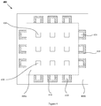
Figure 1 is a schematic top view of an evaporation mask according to Embodiment 1 of the present application; -
Figure 2a is a schematic top view of an OLED panel according to Embodiment 1 of the present application; -
Figure 2b is a schematic front view of the OLED panel according to Embodiment 1 of the present application; -
Figure 3a is a schematic top view of a sheet mask in an evaporation mask according to Embodiment 2 of the present application; -
Figure 3b is a schematic top view of a support strip in an evaporation mask according to Embodiment 2 of the present application; -
Figure 4 is a schematic top view of an OLED panel according to Embodiment 2 of the present application. - 100-evaporation mask; 110-sheet mask; 110a-first functional region; 110b-first peripheral region; 111-first opening; 112-second opening; L1-first edge; L2-second edge;
200-OLED panel; 200a-second functional region; 200b-second peripheral region; 210-observation layer; 220-monitoring structure; 230-functional layer;
300-evaporation mask; 310-sheet mask; 310a-first functional region; 310b-first peripheral region; 311-first opening; 312-second opening; 320-support strip; 321-third opening; L3-first edge; L4-second edge;
400-OLED panel; 400a-second functional region; 400b-second peripheral region; 410-observation layer; 420-monitoring structure; and 430-functional layer. - The evaporation mask, the OLED panel and system, and the evaporation monitoring method proposed in the present application will be described in greater detail below with reference to the drawings and specific embodiments. Advantages and features of the present application will become more apparent from the following description and claims. It should be noted that the drawings are presented in a very simplified form not precisely drawn to scale with the only purpose to facilitate convenience and clarity in explaining the embodiments of the present application.
- Please refer to
Figure 1 , which is a structure diagram of an evaporation mask according to Embodiment 1 of the present application. As shown inFigure 1 , in the embodiment of the present application, theevaporation mask 100 includes a firstfunctional region 110a and a firstperipheral region 110b disposed outside of the firstfunctional region 110a, the firstfunctional region 110a definingfirst openings 111 for forming a functional layer by evaporation, and the firstperipheral region 110b definingsecond openings 112 for monitoring an evaporation effect of thefirst openings 111. In the embodiment of the present application, the functional layer may be any material layer having a certain function and formed by an evaporation process. For example, the functional layer may be an organic material layer having certain capacity of transporting electrons and holes, or a metal layer having certain electrical conductivity, or a dielectric layer having certain insulating property, etc. In the embodiment of the present application, the firstfunctional region 110a may be used for forming a display area of an OLED panel, and the firstperipheral region 110b may be used for forming a non-display area of the OLED panel. - Preferably, the shape of the
second openings 112 is substantially same to that of thefirst openings 111. For example, if thefirst openings 111 are square, thesecond openings 112 are also square. For another example, if thefirst openings 111 are circular, thesecond openings 112 are also circular. Further, the size of thesecond openings 112 is substantially same to that of thefirst openings 111. For example, when thefirst openings 111 and thesecond openings 112 are both square, side lengths of the both are equal. Thus, when the evaporation effect of thefirst openings 111 is monitored through thesecond openings 112, the monitoring result will be more accurate. - Still referring to
Figure 1 , further, the firstperipheral region 110b has a first edge L1 and a second edge L2, opposite to the first edge L1, on each side, wherein the first edge L1 is closer to the firstfunctional region 110a than the second edge L2, and thesecond openings 112 are closer to the first edge L1 than to the second edge L2. Here, thesecond openings 112 are arranged as close as possible to the firstfunctional region 110a, enabling the evaporation effect of thesecond openings 112 to be substantially consistent with the evaporation effect of thefirst openings 111, thus further improving the accuracy of the monitoring result. - In the embodiment of the present application, the
evaporation mask 100 includes asheet mask 110 including a firstfunctional region 110a and a firstperipheral region 110b disposed outside of the firstfunctional region 110a, and thefirst openings 111 and thesecond openings 112 are both located on thesheet mask 110. Further, theevaporation mask 100 further includes a support strip (not shown), and thesheet mask 110 is fixed on the support strip. In the embodiment of the present application, the support strip exposes all thefirst openings 111 and all thesecond openings 112. - In the embodiment of the present application, the
sheet mask 110 is rectangular. Further, the firstfunctional region 110a is also rectangular, and the firstperipheral region 110b is a rectangular ring. A plurality ofsecond openings 112 are provided, being distributed in the firstperipheral region 110b equably. For example, if eightsecond openings 112 are provided, twosecond openings 112 can be uniformly arranged on a strip region of each side of the firstperipheral region 110b. The accuracy of the monitoring result is able to be further improved by monitoring the evaporation effect of thefirst openings 111 through the plurality ofsecond openings 112. - In the embodiment of the present application, the
first openings 111 are used for evaporating monochrome pixels, and the plurality ofsecond openings 112 are used for monitoring the evaporation effect of pixels having the same color as the monochrome pixels evaporated through thefirst openings 111. For example, thefirst openings 111 are used for evaporating red pixels, and the plurality ofsecond openings 112 are all used for monitoring the evaporation effect of the red pixels. For another example, thefirst openings 111 are used for evaporating blue pixels, and the plurality ofsecond openings 112 are all used for monitoring the evaporation effect of the blue pixels. - In the embodiment of the present application,
different evaporation masks 100 are often used for evaporating pixels of different colors. That is, when red pixels are evaporated, oneevaporation mask 100 is used with thesecond openings 112 thereon being used for monitoring the evaporation effect of the red pixels; and when blue pixels are evaporated, anotherevaporation mask 100 is used with thesecond openings 112 thereon being used for monitoring the evaporation effect of the blue pixels. In this case, higher monitoring accuracy can be ensured, at the same time, the manufacturing cost of theevaporation mask 100 is increased. - Correspondingly, the present embodiment further provides an OLED panel. Specifically, please refer to
Figure 2a and Figure 2b , whereinFigure 2a is a schematic top view of an OLED panel according to Embodiment 1 of the present application, andFigure 2b is a schematic front view of the OLED panel according to Embodiment 1 of the present application. As shown inFigure 2a and Figure 2b , theOLED panel 200 includes a secondfunctional region 200a and a secondperipheral region 200b disposed outside of the secondfunctional region 200a, the secondperipheral region 200b having anobservation layer 210 formed thereon. Specifically, theOLED panel 200 may include a glass substrate including a second functional region and a second peripheral region, and theobservation layer 210 may be formed on the glass substrate of the second peripheral region. In the embodiment of the present application, the secondfunctional region 200a may be a display area, and the secondperipheral region 200b may be a non-display area. - Please refer to
Figure 1 ,Figure 2a and Figure 2b , the present embodiment further provides an OLED panel system including theevaporation mask 100 and theOLED panel 200, wherein theevaporation mask 100 is located below theOLED panel 200, thefirst openings 111 of theevaporation mask 100 are used for forming afunctional layer 230 on the secondfunctional area 200a of theOLED panel 200 by evaporation, thesecond openings 112 of theevaporation mask 100 are used for formingmonitoring structures 220 on theobservation layer 210 of theOLED panel 200 by evaporation, and themonitoring structures 220 are used for monitoring the evaporation effect of thefirst openings 111. - In the embodiment of the present application, the monitoring
structures 220 can be easily observed through theobservation layer 210. For example, the material of theobservation layer 210 is a reflective material, thus enabling highlighting of the monitoringstructures 220 to make themonitoring structures 220 easily to be observed, in particular, easily to be captured by an optical device. For another example, the color of theobservation layer 210 is greatly different from that of the monitoringstructures 220, such that the monitoringstructures 220 are easily captured by an optical device. - When the monitoring
structures 220 are formed on theobservation layer 210 of theOLED panel 200 by evaporation through thesecond openings 112 of theevaporation mask 100, (the contour of) themonitoring structures 220 are able to be easily captured, such that the evaporation effect of thefirst openings 111 is easily judged according to themonitoring structures 220. - Preferably, the thickness of the
observation layer 210 is from 100 nm to 200 nm. For example, the thickness of theobservation layer 210 may be 100 nm, 110 nm, 130 nm, 150 nm, 170 nm, 185 nm, or 200 nm, etc. At this thickness, the shape of the monitoringstructures 220 is able to be captured more easily. Further, theobservation layer 210 may be made of silver (Ag), indium tin oxide (ITO), etc. - Still referring to
Figure 2a and Figure 2b , in the embodiment of the present application, theobservation layer 210 covers the entire secondperipheral region 200b. In other embodiments of the present application, theobservation layer 210 may cover only a part of the secondperipheral region 200b. Specifically, the region covered by theobservation layer 210 corresponds to the region evaporated through thesecond openings 112, so that the monitoringstructures 220 are able to be formed on theobservation layer 210. - Preferably, the height difference between the surface of the second
peripheral region 200b and the surface of the secondfunctional region 200a is less than or equals to 200 nm. More preferably, the height difference between the surface of the secondperipheral region 200b and the surface of the secondfunctional region 200a is less than or equals to 100 nm. Thus, monitoring of the evaporation effect of thefirst openings 111 by the monitoringstructures 220 formed on theobservation layer 210 of theOLED panel 200 by evaporation through thesecond openings 112 of theevaporation mask 100 can be further improved. - Specifically, a film layer such as a silicon oxide layer, a silicon nitride layer, a titanium aluminum titanium layer, an organic adhesive layer or the like may be formed on the glass substrate of the second
functional region 200a, and the thickness of the film may be from 5µm to 10µm. Correspondingly, a silicon oxide layer, a silicon nitride layer, a titanium aluminum titanium layer, an organic adhesive layer or the like may also be formed on the glass substrate of the secondperipheral region 200b, and then theobservation layer 210 is further formed thereon. The silicon oxide layer, the silicon nitride layer, the titanium aluminum titanium layer, the organic adhesive layer or the like on the glass substrate of the secondperipheral region 200b may be formed at the same time as the silicon oxide layer, the silicon nitride layer, the titanium aluminum titanium layer, the organic adhesive layer or the like on the glass substrate of the secondfunctional region 200a. Thus, height of the surface of the secondperipheral region 200b and height of the surface of the secondfunctional region 200a are ensured to be similar as well as an additional process step is able to be avoided. - In the embodiment of the present application, the monitoring
structures 220 can be formed on theobservation layer 210 of theOLED panel 200 by evaporation through thesecond openings 112 of theevaporation mask 100, and the evaporation effect of thefirst openings 111 of theevaporation mask 100 can be monitored through the monitoringstructures 220, so that the evaporation effect is able to be monitored in time to achieve real-time on-line monitoring. - Correspondingly, the present embodiment further provides an evaporation monitoring method, including:
- forming a
functional layer 230 andmonitoring structures 220 on theOLED panel 200 using theevaporation mask 100; - acquiring actual centers of the monitoring
structures 220 on theOLED panel 200; and - comparing the actual centers of the monitoring
structures 220 with theoretical centers of the monitoringstructures 220 to obtain an evaporation effect offirst openings 111 of theevaporation mask 100. - The actual centers of the monitoring
structures 220 on theOLED panel 200 can be acquired in the following way: capturing (the contour or boundary of) themonitoring structures 220 by an image capturing device (e.g., a camera or a video, etc.), and then calculating centers of the capturedmonitoring structures 220 according to the capturedmonitoring structures 220, i.e., acquiring the actual centers of the monitoringstructures 220. It is readily known that after the contour or boundary of the monitoringstructures 220 is obtained, the centers thereof are easily obtained by calculation. For example, if themonitoring structure 220 is square, the intersection of two diagonals is the center of themonitoring structure 220. For another example, if themonitoring structure 220 is circular, the center of circle thereof is the center of themonitoring structure 220. - In the embodiment of the present application, when the actual centers of the monitoring
structures 220 and the theoretical centers of the monitoringstructures 220 are at the same positions, the evaporation through thesecond openings 112 has no offset, thus inferring that the evaporation through thefirst openings 111 also has no offset; and when the actual centers of the monitoringstructures 220 and the theoretical centers of the monitoringstructures 220 are at different positions, the evaporation through thesecond openings 112 has offset, thus inferring that the evaporation through thefirst openings 111 also has offset. The comparison of positions of the actual centers and theoretical centers of the monitoringstructures 220 can be achieved by comparing coordinates of the two. - Further, the above evaporation monitoring method can be implemented by a terminal device having an image capturing function and a calculation function, so that the entire evaporation monitoring is very convenient, efficient and accurate.
- Further, the present embodiment also provides an evaporation adjusting method, including:
- obtaining an evaporation effect of
first openings 111 of theevaporation mask 100 on theOLED panel 200 using the above evaporation monitoring method; and - adjusting the position of the
evaporation mask 100 relative to the position of theOLED panel 200 when the evaporation through thefirst openings 111 has offset. - In the embodiment of the present application, for example, when the actual centers of the monitoring
structures 220 and the theoretical centers of the monitoringstructures 220 are compared and the actual centers of the monitoringstructures 220 are found located on first sides of the theoretical centers of the monitoringstructures 220, the position of theOLED panel 200 can be kept unchanged with theevaporation mask 100 being moved toward second sides, opposite to the first sides, of the theoretical centers, so that the adjustment of theevaporation mask 100 is able to be achieved to improve the subsequent evaporation effect. - To sum up, in the evaporation mask, the OLED panel and system, the evaporation monitoring method and adjusting method provided by the embodiment of the present application, monitoring structures can be formed on the observation layer of the OLED panel by evaporation through the second openings of the evaporation mask, and the evaporation effect of the first openings of the evaporation mask can be monitored through the monitoring structures, so that the evaporation effect is able to be monitored in time to achieve real-time on-line monitoring.
- Please refer to
Figure 3a , which is a schematic top view of a sheet mask in an evaporation mask according to Embodiment 2 of the present application. As shown inFigure 3a , in the embodiment of the present application, theevaporation mask 300 includes a firstfunctional region 310a and a firstperipheral region 310b disposed outside of the firstfunctional region 310a definingfirst openings 311 for forming a functional layer by evaporation, and the firstperipheral region 310b definingsecond openings 312 for monitoring an evaporation effect of thefirst openings 311. In the embodiment of the present application, the functional layer may be any layer made of the material having a certain function and formed by an evaporation process. For example, the functional layer may be an organic layer having certain electron or hole transport capability, or a metal layer having certain electrical conductivity, or a dielectric layer having certain insulating property, etc. In the embodiment of the present application, the firstfunctional region 310a may be used for forming a display area of an OLED panel, and the firstperipheral region 310b may be used for forming a non-display area of the OLED panel. - Preferably, the shape of the
second openings 312 is substantially same to that of thefirst openings 311. For example, if thefirst openings 311 are square, thesecond openings 312 are also square. For another example, if thefirst openings 311 are circular, thesecond openings 312 are also circular. Further, the size of thesecond openings 312 is substantially same to that of thefirst openings 311. For example, when thefirst openings 311 and thesecond openings 312 are both square, the side lengths of the two are equal; and when thefirst openings 311 and thesecond openings 312 are both circular, the diameters of the two are also equal. Thus, the monitoring result will be more accurate when the evaporation effect of thefirst openings 311 is monitored through thesecond openings 312. - Still referring to
Figure 3a , further, the firstperipheral region 310b has a first edge L3 and a second edge L4, opposite to the first edge L3, on each side. The first edge L3 is closer to the firstfunctional region 310a than the second edge L4 to the firstfunctional region 310a, and thesecond openings 312 are closer to the first edge L3 than to the second edge L4. Here, thesecond openings 312 are arranged as close as possible to the firstfunctional region 310a, so that the evaporation effect of thesecond openings 312 is substantially consistent with the evaporation effect of thefirst openings 311, thus further improving the accuracy of the monitoring result. - In the embodiment of the present application, the
evaporation mask 300 includes a sheet mask 310comprising a firstfunctional region 310a and a firstperipheral region 310b disposed outside of the firstfunctional region 310a, and thefirst openings 311 and thesecond openings 312 are all located on thesheet mask 310. - In the embodiment of the present application, the
sheet mask 310 is rectangular. Further, the firstfunctional region 310a is also rectangular, and the firstperipheral region 310b is a rectangular ring. A plurality ofsecond openings 312 are provided, being distributed in the firstperipheral region 310b equably. For example, if twelvesecond openings 312 are provided, three of thesecond openings 312 can be uniformly arranged on a strip region of each side of the firstperipheral region 310b. The accuracy of the monitoring result is able to be further improved by monitoring the evaporation effect of thefirst openings 311 through the plurality ofsecond openings 312. - In the embodiment of the present application, the
first openings 311 are used for evaporating monochrome pixels, and the plurality ofsecond openings 312 are used for monitoring the evaporation effects of pixels having different colors. For example, thefirst openings 311 are used for evaporating red pixels, and some of thesecond openings 312 are used for monitoring the evaporation effect of the red pixels. For another example, thefirst openings 311 are used for evaporating blue pixels, and some of thesecond openings 312 are used for monitoring the evaporation effect of the blue pixels. - In the embodiment of the present application, the
same evaporation mask 300 can be used for evaporating pixels having different colors. That is, when red pixels are evaporated, anevaporation mask 300 is used, and some of thesecond openings 312 thereon are used for monitoring the evaporation effect of the red pixels; and when blue pixels are evaporated, theevaporation mask 300 is still used, and some of thesecond openings 312 thereon are used for monitoring the evaporation effect of the blue pixels, wherein some of thesecond openings 312 for monitoring the evaporation effect of the blue pixels is different from some of thesecond openings 312 for monitoring the evaporation effect of the red pixels (i.e., none of second openings is shared). In this case, not only can the evaporation effect of thefirst openings 311 be monitored, but also the manufacturing cost of theevaporation mask 300 is not increased. - In the embodiment of the present application, the plurality of
second openings 312 are used for monitoring evaporation effects of different colors of pixels. For example, some ofsecond openings 312 can be used for monitoring the evaporation effect of red pixels, some of thesecond openings 312 can be used for monitoring the evaporation effect of blue pixels, and some of thesecond openings 312 can be used for monitoring the evaporation effect of green pixels. Thus, when different colors of pixels are evaporated and the evaporation effects of thefirst openings 311 are monitored using thesecond openings 312, only some of thesecond openings 312 corresponding to the first openings 311can be used, and the remainingsecond openings 312 non-corresponding to thefirst openings 311 are ignored. - Next, please refer to
Figure 3b , which is a schematic top view of a support strip in the evaporation mask according to Embodiment 2 of the present application. As shown inFigure 3b , theevaporation mask 300 further includes asupport strip 320 for supporting thesheet mask 310, wherein thesupport strip 320 has athird opening 321 exposing only some of thesecond openings 312, and the exposedsecond openings 312 are used for monitoring the evaporation effect of pixels having the same color as the monochrome pixels evaporated through thefirst openings 311. That is, in an implementation of the embodiment of the present application, thesecond openings 312 that are temporarily not used are sheltered by thesupport strip 320. For example, when thefirst openings 311 are used for evaporating red pixels, thethird opening 321 of thesupport strip 320 exposes only some of thesecond openings 312 for monitoring the evaporation effect of the red pixels, some of thesecond openings 312 for monitoring the evaporation effect of blue pixels and some of thesecond openings 312 for monitoring the evaporation effect of green pixels are sheltered by thesupport strip 320. In this case, when different colors of pixels are evaporated, thesupport strip 320 is often replaced or changed such that thethird openings 321 on thesupport strip 320 expose different ones of thesecond openings 312. Due to the relatively low cost of the support strip, this method is able to ensure high monitoring accuracy and relatively low cost. - Correspondingly, the present embodiment further provides an OLED panel. Specifically, please refer to
Figure 4 , which is a schematic top view of an OLED panel according to Embodiment 2 of the present application. As shown inFigure 4 , theOLED panel 400 includes a secondfunctional region 400a and a secondperipheral region 400b disposed outside of the secondfunctional region 400a, and anobservation layer 410 is formed on the secondperipheral region 400b. Specifically, theOLED panel 400 may include a glass substrate including a second functional region and a second peripheral region, and theobservation layer 410 may be formed on the glass substrate of the second peripheral region. In the embodiment of the present application, the secondfunctional region 400a may be a display area, and the secondperipheral region 400b may be a non-display area. - Please refer to
Figure 3a, Figure 3b andFigure 4 , the present embodiment further provides an OLED panel system including theevaporation mask 300 and theOLED panel 400, wherein theevaporation mask 300 is located below theOLED panel 400, thefirst openings 311 of theevaporation mask 300 are used for forming afunctional layer 430 on the secondfunctional area 400a of theOLED panel 400 by evaporation, thesecond openings 312 of theevaporation mask 300 are used for formingmonitoring structures 420 on theobservation layer 410 of theOLED panel 400 by evaporation, and themonitoring structures 420 are used for monitoring the evaporation effect of thefirst openings 311. - In the embodiment of the present application, the monitoring
structures 420 are able to be easily observed through theobservation layer 410. For example, the material made of theobservation layer 410 is reflective to enable highlighting of the monitoringstructures 420, thus enabling the monitoringstructures 420 to be easily observed, and particularly, to be easily captured by an optical device. For another example, the color of theobservation layer 410 is greatly different from that of the monitoringstructures 420, thus enabling the monitoringstructures 420 to be easily captured by the optical device. - When the monitoring
structures 420 are formed on theobservation layer 410 of theOLED panel 400 by evaporation through thesecond openings 312 of theevaporation mask 300, (the contour of) themonitoring structures 420 are able to be easily captured, such that the evaporation effect of thefirst openings 311 are able to be easily judged according to themonitoring structures 420. - Preferably, the thickness of the
observation layer 410 is from 100 nm to 200 nm. For example, the thickness of theobservation layer 410 may be 100 nm, 110 nm, 130 nm, 150 nm, 170 nm, 185 nm, or 200 nm, etc. At this thickness, the shape of the monitoringstructures 420 is able to be captured more easily. Further, theobservation layer 410 may be made of silver (Ag), indium tin oxide (ITO), etc. - Still referring to
Figure 4 , in the embodiment of the present application, theobservation layer 410 covers only a part of the secondperipheral region 200b. Specifically, the region covered by theobservation layer 410 corresponds to the region evaporated through thesecond openings 312, and preferably, the region covered by theobservation layer 410 is greater than or equals to the region evaporated through thesecond openings 312, so that the monitoringstructures 420 are able to be formed on theobservation layer 410. In other embodiments of the present application, theobservation layer 410 may also cover the entire secondperipheral region 400b. - Preferably, the height difference between the surface of the second
peripheral region 400b and the surface of the secondfunctional region 400a is less than or equals to 200 nm. More preferably, the height difference between the surface of the secondperipheral region 400b and the surface of the secondfunctional region 400a is less than or equals to 100 nm. Thus, monitoring of the evaporation effect of thefirst openings 311 by the monitoringstructures 420 formed on theobservation layer 410 of theOLED panel 400 by evaporation through thesecond openings 312 of theevaporation mask 300 can be further improved. - Specifically, a film such as a silicon oxide layer, a silicon nitride layer, a titanium aluminum titanium layer, an organic adhesive layer or the like may be formed on the glass substrate of the second
functional region 400a, and the thickness of the film may be from 5µm to 10µm. Correspondingly, a silicon oxide layer, a silicon nitride layer, a titanium aluminum titanium layer, an organic adhesive layer or the like may also be formed on the glass substrate of the secondperipheral region 400b, and then theobservation layer 410 is further formed thereon. The silicon oxide layer, the silicon nitride layer, the titanium aluminum titanium layer, the organic adhesive layer or the like on the glass substrate of the secondperipheral region 400b may be formed at the same time as the silicon oxide layer, the silicon nitride layer, the titanium aluminum titanium layer, the organic adhesive layer or the like on the glass substrate of the secondfunctional region 400a. Thus, height of the surface of the secondperipheral region 400b and that of the surface of the secondfunctional region 400a are ensured to be similar, as well as an additional process steps is able to be avoided. - In the embodiment of the present application, the monitoring
structures 420 can be formed on theobservation layer 410 of theOLED panel 400 by evaporation through thesecond openings 312 of theevaporation mask 300, and the evaporation effect of thefirst openings 311 of theevaporation mask 300 can be monitored through the monitoringstructures 420, so that the evaporation effect is able to be monitored in time to achieve real-time on-line monitoring. - Correspondingly, the present embodiment further provides an evaporation monitoring method, including:
- forming a
functional layer 430 andmonitoring structures 420 on theOLED panel 400 using theevaporation mask 300; - acquiring actual centers of the monitoring
structures 420 on theOLED panel 400; and - comparing the actual centers of the monitoring
structures 420 with theoretical centers of the monitoringstructures 420 to obtain an evaporation effect offirst openings 311 of theevaporation mask 300. - The actual centers of the monitoring
structures 420 on theOLED panel 400 can be acquired in the following way: capturing (the contour or boundary of) themonitoring structures 420 by an image capturing device (e.g., a camera or a video, etc.), and then calculating centers of the capturedmonitoring structures 420 according to the capturedmonitoring structures 420, i.e., acquiring the actual centers of the monitoringstructures 420. It is readily known that after the contour or boundary of the monitoringstructures 420 is obtained, the centers thereof are easily obtained by calculation. For example, if themonitoring structure 420 is square, the intersection of two diagonals is the center of themonitoring structure 420. For another example, if themonitoring structure 420 is circular, the center of circle thereof is the center of themonitoring structure 420. - In the embodiment of the present application, when the actual centers of the monitoring
structures 420 and the theoretical centers of the monitoringstructures 420 are at the same positions, the evaporation through thesecond openings 312 has no offset, thus inferring that the evaporation through thefirst openings 311 also has no offset; and when the actual centers of the monitoringstructures 420 and the theoretical centers of the monitoringstructures 420 are at different positions, the evaporation through thesecond openings 312 has offset, thus inferring that the evaporation through thefirst openings 311 also has offset. The comparison of positions of the actual centers and theoretical centers of the monitoringstructures 420 can be achieved by comparing coordinates of the two. - Further, the above evaporation monitoring method can be implemented by a terminal device having an image capturing function and a calculation function, so that the entire evaporation monitoring is very convenient, efficient and accurate.
- Further, the present embodiment also provides an evaporation adjusting method, including:
- obtaining an evaporation effect of
first openings 311 of theevaporation mask 300 on theOLED panel 400 using the above evaporation monitoring method; and - adjusting the position of the
evaporation mask 300 relative to the position of theOLED panel 400 when the evaporation through thefirst openings 311 has offset. - In the embodiment of the present application, for example, when the actual centers of the monitoring
structures 420 and the theoretical centers of the monitoringstructures 420 are compared and the actual centers of the monitoringstructures 420 are found located on first sides of the theoretical centers of the monitoringstructures 420, the position of theOLED panel 400 can be kept unchanged with theevaporation mask 300 being moved toward second sides, opposite to the first sides, of the theoretical centers, so that the adjustment of theevaporation mask 300 is able to be achieved to improve the subsequent evaporation effect. - To sum up, in the evaporation mask, the OLED panel and system, the evaporation monitoring method and adjusting method provided by the embodiment of the present application, monitoring structures can be formed on the observation layer of the OLED panel by evaporation through the second openings of the evaporation mask, and the evaporation effect of the first openings of the evaporation mask can be monitored through the monitoring structures, so that the evaporation effect is able to be monitored in time to achieve real-time on-line monitoring.
- Described above are merely preferred embodiments of the present application, and the scope of the present application is not limited in any way. Any change or modification made by those skilled in the art concerning the foregoing disclosure fall within the scope of the appended claims.
Claims (12)
- An evaporation mask, comprising: a first functional region and a first peripheral region disposed outside of the first functional region, the first functional region defining at least one first opening for forming a functional layer on an OLED panel by evaporation, the first peripheral region defining at least one second opening for forming a monitoring structure on the OLED panel by evaporation, an evaporation effect of the at least one first opening being monitored via the monitoring structure.
- The evaporation mask of claim 1, wherein a shape of the at least one second opening is substantially same to a shape of the at least one first opening.
- The evaporation mask of claim 1 or 2, wherein the first peripheral region has a first edge and a second edge opposite to the first edge, wherein the first edge is closer to the first functional region than the second edge to the first functional region, and each of the second openings is closer to the first edge than to the second edge.
- The evaporation mask of claim 1 or 2, wherein a plurality of second openings are provided, being distributed in the first peripheral region equably.
- The evaporation mask of claim 4, further comprising a sheet mask and a support strip for supporting the sheet mask, wherein the at least one first opening and the plurality of second openings are all located on the sheet mask, and the support strip has at least one third opening exposing at least one of the plurality of second openings corresponding to the at least one third opening.
- An OLED panel, comprising a second functional region and a second peripheral region disposed outside of the second functional region, the second peripheral region having an observation layer formed thereon, the second functional region having a functional layer formed thereon by evaporation through at least one first opening of an evaporation mask, the observation layer of the OLED panel having at least one monitoring structure formed thereon by evaporation through at least one second opening of the evaporation mask, an evaporation effect of the at least one first opening being monitored via the monitoring structure.
- The OLED panel of claim 6, wherein the observation layer is made of a reflective material.
- The OLED panel of claim 6 or 7, wherein a thickness of the observation layer is from 100 nm to 200 nm.
- The OLED panel of claim 6 or 7, wherein a height difference between a surface of the second peripheral region and a surface of the second functional region is less than or equals to 200 nm.
- An OLED panel system, comprising:an evaporation mask, comprising a first functional region and a first peripheral region disposed outside of the first functional region, the first functional region defining at least one first opening, the first peripheral region defining at least one second opening; andan OLED panel, arranged above the evaporation mask, the OLED panel comprising a second functional region and a second peripheral region disposed outside of the second functional region, an observation layer being formed on the second peripheral region,the second functional region of the OLED panel having a functional layer formed thereon by evaporation through the at least one first opening of the evaporation mask, the observation layer of the OLED panel having at least one monitoring structure formed thereon by evaporation through the at least one second opening of the evaporation mask, and an evaporation effect of the at least one first opening being monitored via the monitoring structure.
- A method for evaporation monitoring, comprising:providing an evaporation mask, the evaporation mask comprising a first functional region and a first peripheral region disposed outside of the first functional region, the first functional region defining at least one first opening, the first peripheral region defining at least one second opening;providing an OLED panel, the OLED panel comprising a second functional region and a second peripheral region disposed outside of the second functional region, the second peripheral region having an observation layer formed thereon;forming a functional layer and at least one monitoring structure on the second functional region and the observation layer of the OLED panel respectively using the evaporation mask;acquiring an actual center of the at least one monitoring structure on the OLED panel; andcomparing the actual center of the monitoring structure with a theoretical center of the monitoring structure to obtain an evaporation effect of the at least one first opening of the evaporation mask.
- The method for evaporation monitoring of claim 11, wherein the evaporation through the at least one first opening is considered to have no offset when the actual center of the monitoring structure and the theoretical center of the monitoring structure are at the same position, and the evaporation through the at least one first opening is considered to have offset when the actual center of the monitoring structure and the theoretical center of the monitoring structure are at different positions.
Applications Claiming Priority (2)
| Application Number | Priority Date | Filing Date | Title |
|---|---|---|---|
| CN201710910812.3A CN109585695B (en) | 2017-09-29 | 2017-09-29 | Evaporation mask plate, OLED panel, system and evaporation monitoring method |
| PCT/CN2018/085015 WO2019062116A1 (en) | 2017-09-29 | 2018-04-28 | Vapor deposition mask, oled panel, system, and vapor deposition monitoring method |
Publications (3)
| Publication Number | Publication Date |
|---|---|
| EP3690974A1 true EP3690974A1 (en) | 2020-08-05 |
| EP3690974A4 EP3690974A4 (en) | 2020-11-25 |
| EP3690974B1 EP3690974B1 (en) | 2025-02-26 |
Family
ID=65431126
Family Applications (1)
| Application Number | Title | Priority Date | Filing Date |
|---|---|---|---|
| EP18863666.6A Active EP3690974B1 (en) | 2017-09-29 | 2018-04-28 | Vapor deposition monitoring method |
Country Status (7)
| Country | Link |
|---|---|
| US (1) | US11374173B2 (en) |
| EP (1) | EP3690974B1 (en) |
| JP (1) | JP7051251B2 (en) |
| KR (1) | KR102194553B1 (en) |
| CN (1) | CN109585695B (en) |
| TW (1) | TWI662731B (en) |
| WO (1) | WO2019062116A1 (en) |
Families Citing this family (9)
| Publication number | Priority date | Publication date | Assignee | Title |
|---|---|---|---|---|
| CN109585695B (en) * | 2017-09-29 | 2020-01-24 | 昆山国显光电有限公司 | Evaporation mask plate, OLED panel, system and evaporation monitoring method |
| CN109554665B (en) * | 2019-01-22 | 2021-01-15 | 京东方科技集团股份有限公司 | Evaporation method, evaporation mask module, display panel and display device |
| CN110643938B (en) * | 2019-10-31 | 2022-07-05 | 京东方科技集团股份有限公司 | Mask plate assembly |
| KR102836687B1 (en) | 2020-05-11 | 2025-07-22 | 삼성디스플레이 주식회사 | Mask inspection apparatus and mask inspection method using the same |
| CN111748767A (en) * | 2020-06-24 | 2020-10-09 | 武汉华星光电半导体显示技术有限公司 | Evaporation device and preparation method of display panel |
| CN111816685B (en) * | 2020-07-22 | 2022-12-13 | 京东方科技集团股份有限公司 | Display substrate, test method thereof and display device |
| CN114381688B (en) * | 2021-12-30 | 2024-04-23 | 昆山工研院新型平板显示技术中心有限公司 | Mask assembly, mask, vapor deposition boundary confirmation and vapor deposition deviation correction method |
| CN121986182A (en) * | 2023-09-07 | 2026-05-05 | 应用材料公司 | Deposition system, shielding assembly, substrate coating method and substrate |
| WO2025059838A1 (en) * | 2023-09-19 | 2025-03-27 | 京东方科技集团股份有限公司 | Array substrate and display apparatus |
Family Cites Families (23)
| Publication number | Priority date | Publication date | Assignee | Title |
|---|---|---|---|---|
| KR100469251B1 (en) | 2002-04-12 | 2005-02-02 | 엘지전자 주식회사 | Glass Shadow Mask and Organic Electroluminescence Display Device Using the same |
| TWI223007B (en) | 2003-04-03 | 2004-11-01 | Prodisc Technology Inc | Coating apparatus |
| CN1234906C (en) | 2003-04-11 | 2006-01-04 | 精碟科技股份有限公司 | Coating equipment |
| KR100716704B1 (en) * | 2004-03-03 | 2007-05-14 | 산요덴키가부시키가이샤 | Measurement method of deposition thickness, formation method of material layer, deposition thickness measurement device and material layer formation device |
| JP4614784B2 (en) | 2005-02-07 | 2011-01-19 | 大日本印刷株式会社 | Metal mask and mask unit |
| US20080284690A1 (en) * | 2007-05-18 | 2008-11-20 | Sam Min Ko | Organic light emitting display device |
| JP2009158328A (en) * | 2007-12-27 | 2009-07-16 | Seiko Epson Corp | Manufacturing method of organic EL device, inspection method of organic EL device |
| EP2479311B1 (en) * | 2009-09-15 | 2017-04-05 | Sharp Kabushiki Kaisha | Vapor deposition method |
| JP2013209700A (en) * | 2012-03-30 | 2013-10-10 | Hitachi High-Technologies Corp | Vacuum vapor deposition apparatus and vacuum vapor deposition method |
| JP2013211139A (en) * | 2012-03-30 | 2013-10-10 | Hitachi High-Technologies Corp | Deposition device and deposition method |
| KR20190041043A (en) * | 2013-04-22 | 2019-04-19 | 어플라이드 머티어리얼스, 인코포레이티드 | Actively-aligned fine metal mask |
| CN105280842B (en) * | 2014-07-25 | 2017-07-25 | 上海和辉光电有限公司 | Method for measuring subpixel offset in OLED manufacturing process |
| CN105702880B (en) * | 2014-11-28 | 2018-04-17 | 上海和辉光电有限公司 | Optical registration compensation device, compactness detection device, deposition system and its method |
| KR102411542B1 (en) * | 2015-05-19 | 2022-06-22 | 삼성디스플레이 주식회사 | Pattern forming method for pixel and pixel position accuracy inspection and the mask for the same |
| CN204714884U (en) * | 2015-06-04 | 2015-10-21 | 昆山国显光电有限公司 | The device of adjustment evaporation off normal |
| KR102427670B1 (en) | 2015-10-16 | 2022-08-02 | 삼성디스플레이 주식회사 | Mask frame assembly and manufacturing method of organic light emittion dioed display using the same |
| WO2017138166A1 (en) * | 2016-02-10 | 2017-08-17 | 鴻海精密工業股▲ふん▼有限公司 | Vapor depositin mask manufacturing method, vapor deposition mask, and organic semiconductor element manufacturing method |
| TWI579396B (en) | 2016-03-18 | 2017-04-21 | 萬國半導體股份有限公司 | Method of monitoring epitaxial growth geometry shift |
| CN106129270B (en) | 2016-07-01 | 2018-06-12 | 武汉华星光电技术有限公司 | Monitor method and substrate that mask plate forms pattern position |
| CN106086786B (en) | 2016-08-19 | 2018-06-05 | 京东方科技集团股份有限公司 | offset calibration method and system |
| CN206015074U (en) | 2016-09-23 | 2017-03-15 | 昆山国显光电有限公司 | Precision metallic shade and oled substrate |
| CN106637074B (en) * | 2017-01-09 | 2019-02-22 | 昆山国显光电有限公司 | The method that mask plate, oled substrate and measurement vapor deposition pixel deviation is deposited |
| CN109585695B (en) * | 2017-09-29 | 2020-01-24 | 昆山国显光电有限公司 | Evaporation mask plate, OLED panel, system and evaporation monitoring method |
-
2017
- 2017-09-29 CN CN201710910812.3A patent/CN109585695B/en active Active
-
2018
- 2018-04-28 WO PCT/CN2018/085015 patent/WO2019062116A1/en not_active Ceased
- 2018-04-28 EP EP18863666.6A patent/EP3690974B1/en active Active
- 2018-04-28 KR KR1020197021580A patent/KR102194553B1/en active Active
- 2018-04-28 US US16/323,062 patent/US11374173B2/en active Active
- 2018-04-28 JP JP2019562456A patent/JP7051251B2/en active Active
- 2018-05-09 TW TW107115759A patent/TWI662731B/en active
Also Published As
| Publication number | Publication date |
|---|---|
| KR102194553B1 (en) | 2020-12-23 |
| EP3690974A4 (en) | 2020-11-25 |
| JP2020506299A (en) | 2020-02-27 |
| US20210336146A1 (en) | 2021-10-28 |
| US11374173B2 (en) | 2022-06-28 |
| CN109585695B (en) | 2020-01-24 |
| WO2019062116A1 (en) | 2019-04-04 |
| CN109585695A (en) | 2019-04-05 |
| TWI662731B (en) | 2019-06-11 |
| KR20190095456A (en) | 2019-08-14 |
| JP7051251B2 (en) | 2022-04-11 |
| TW201842696A (en) | 2018-12-01 |
| EP3690974B1 (en) | 2025-02-26 |
Similar Documents
| Publication | Publication Date | Title |
|---|---|---|
| US11374173B2 (en) | Evaporation mask, OLED panel and system, and evaporation monitoring method | |
| KR102784718B1 (en) | Display apparatus and method for manufacturing the same | |
| US11578400B2 (en) | Fine metal mask having protective portions having protective portion with ratio of thickness reduction equal to single pixel aperture ratio and method for manufacturing the same, mask frame assembly | |
| US10829847B2 (en) | Mask plate and method for fabricating the same | |
| EP3726580B1 (en) | Display substrate, manufacturing method therefor and display device | |
| US6626721B1 (en) | Organic electroluminescent device with supplemental cathode bus conductor | |
| US11502135B2 (en) | Display substrate, display panel and display device | |
| WO2020151073A1 (en) | Method for fabricating oled display panel | |
| WO2016004698A1 (en) | Oled display device and manufacturing method thereof, display device and evaporation-deposition mask plate | |
| US12114534B2 (en) | OLED display substrate, manufacturing method thereof, and display device | |
| CN110911584B (en) | Organic light-emitting display panel, manufacturing method thereof and display device | |
| CN100379057C (en) | Separate type shielding mask device for manufacturing organic light emitting diode display | |
| CN109449314A (en) | Display base plate and its manufacturing method, display panel | |
| CN112962055B (en) | Mask plate, display substrate evaporation components and display substrate | |
| CN113016073A (en) | Mask plate, manufacturing method thereof and organic light-emitting device | |
| TWI736193B (en) | A mask assembly and a display device | |
| US8013524B2 (en) | Organic EL display | |
| KR20150031819A (en) | Method for depositing thin film and method for fabricating organic light emitting display device using the same | |
| CN119592907B (en) | Mask assembly, preparation method and evaporation equipment | |
| US20240081136A1 (en) | System and Method for Direct Patterning Using a Compensated Shadow Mask | |
| US20220173320A1 (en) | Mask and method for preparing same, and method for preparing display panel | |
| JP2022013772A (en) | Mask inspection device and mask inspection method | |
| JP2762995B2 (en) | Organic EL device | |
| CN119592907A (en) | Mask assembly, preparation method and evaporation equipment | |
| US20190372059A1 (en) | Display device producing method, vapor deposition mask and active matrix substrate |
Legal Events
| Date | Code | Title | Description |
|---|---|---|---|
| STAA | Information on the status of an ep patent application or granted ep patent |
Free format text: STATUS: THE INTERNATIONAL PUBLICATION HAS BEEN MADE |
|
| PUAI | Public reference made under article 153(3) epc to a published international application that has entered the european phase |
Free format text: ORIGINAL CODE: 0009012 |
|
| STAA | Information on the status of an ep patent application or granted ep patent |
Free format text: STATUS: REQUEST FOR EXAMINATION WAS MADE |
|
| 17P | Request for examination filed |
Effective date: 20190806 |
|
| AK | Designated contracting states |
Kind code of ref document: A1 Designated state(s): AL AT BE BG CH CY CZ DE DK EE ES FI FR GB GR HR HU IE IS IT LI LT LU LV MC MK MT NL NO PL PT RO RS SE SI SK SM TR |
|
| AX | Request for extension of the european patent |
Extension state: BA ME |
|
| A4 | Supplementary search report drawn up and despatched |
Effective date: 20201028 |
|
| RIC1 | Information provided on ipc code assigned before grant |
Ipc: C23C 14/24 20060101ALI20201022BHEP Ipc: H01L 51/56 20060101AFI20201022BHEP Ipc: H01L 51/00 20060101ALI20201022BHEP Ipc: H01L 21/67 20060101ALI20201022BHEP Ipc: C23C 14/04 20060101ALI20201022BHEP Ipc: H01L 23/544 20060101ALI20201022BHEP Ipc: H01L 27/32 20060101ALI20201022BHEP |
|
| DAV | Request for validation of the european patent (deleted) | ||
| DAX | Request for extension of the european patent (deleted) | ||
| STAA | Information on the status of an ep patent application or granted ep patent |
Free format text: STATUS: EXAMINATION IS IN PROGRESS |
|
| 17Q | First examination report despatched |
Effective date: 20220829 |
|
| REG | Reference to a national code |
Ref country code: DE Ref legal event code: R079 Free format text: PREVIOUS MAIN CLASS: H01L0051560000 Ipc: C23C0014040000 Ref country code: DE Ref legal event code: R079 Ref document number: 602018079682 Country of ref document: DE Free format text: PREVIOUS MAIN CLASS: H01L0051560000 Ipc: C23C0014040000 |
|
| GRAP | Despatch of communication of intention to grant a patent |
Free format text: ORIGINAL CODE: EPIDOSNIGR1 |
|
| STAA | Information on the status of an ep patent application or granted ep patent |
Free format text: STATUS: GRANT OF PATENT IS INTENDED |
|
| RIC1 | Information provided on ipc code assigned before grant |
Ipc: H10K 71/16 20230101ALI20240923BHEP Ipc: H10K 59/88 20230101ALI20240923BHEP Ipc: C23C 14/54 20060101ALI20240923BHEP Ipc: C23C 14/04 20060101AFI20240923BHEP |
|
| INTG | Intention to grant announced |
Effective date: 20241029 |
|
| RIN1 | Information on inventor provided before grant (corrected) |
Inventor name: GAO, FENG Inventor name: WANG, XULIANG Inventor name: LI, JUNFENG Inventor name: LIU, MINGXING |
|
| GRAS | Grant fee paid |
Free format text: ORIGINAL CODE: EPIDOSNIGR3 |
|
| GRAA | (expected) grant |
Free format text: ORIGINAL CODE: 0009210 |
|
| STAA | Information on the status of an ep patent application or granted ep patent |
Free format text: STATUS: THE PATENT HAS BEEN GRANTED |
|
| AK | Designated contracting states |
Kind code of ref document: B1 Designated state(s): AL AT BE BG CH CY CZ DE DK EE ES FI FR GB GR HR HU IE IS IT LI LT LU LV MC MK MT NL NO PL PT RO RS SE SI SK SM TR |
|
| REG | Reference to a national code |
Ref country code: GB Ref legal event code: FG4D |
|
| REG | Reference to a national code |
Ref country code: CH Ref legal event code: EP |
|
| REG | Reference to a national code |
Ref country code: DE Ref legal event code: R096 Ref document number: 602018079682 Country of ref document: DE |
|
| REG | Reference to a national code |
Ref country code: IE Ref legal event code: FG4D |
|
| REG | Reference to a national code |
Ref country code: NL Ref legal event code: MP Effective date: 20250226 |
|
| PG25 | Lapsed in a contracting state [announced via postgrant information from national office to epo] |
Ref country code: RS Free format text: LAPSE BECAUSE OF FAILURE TO SUBMIT A TRANSLATION OF THE DESCRIPTION OR TO PAY THE FEE WITHIN THE PRESCRIBED TIME-LIMIT Effective date: 20250526 |
|
| PG25 | Lapsed in a contracting state [announced via postgrant information from national office to epo] |
Ref country code: FI Free format text: LAPSE BECAUSE OF FAILURE TO SUBMIT A TRANSLATION OF THE DESCRIPTION OR TO PAY THE FEE WITHIN THE PRESCRIBED TIME-LIMIT Effective date: 20250226 |
|
| PG25 | Lapsed in a contracting state [announced via postgrant information from national office to epo] |
Ref country code: PL Free format text: LAPSE BECAUSE OF FAILURE TO SUBMIT A TRANSLATION OF THE DESCRIPTION OR TO PAY THE FEE WITHIN THE PRESCRIBED TIME-LIMIT Effective date: 20250226 |
|
| PGFP | Annual fee paid to national office [announced via postgrant information from national office to epo] |
Ref country code: DE Payment date: 20250411 Year of fee payment: 8 |
|
| PG25 | Lapsed in a contracting state [announced via postgrant information from national office to epo] |
Ref country code: ES Free format text: LAPSE BECAUSE OF FAILURE TO SUBMIT A TRANSLATION OF THE DESCRIPTION OR TO PAY THE FEE WITHIN THE PRESCRIBED TIME-LIMIT Effective date: 20250226 |
|
| REG | Reference to a national code |
Ref country code: LT Ref legal event code: MG9D |
|
| PG25 | Lapsed in a contracting state [announced via postgrant information from national office to epo] |
Ref country code: IS Free format text: LAPSE BECAUSE OF FAILURE TO SUBMIT A TRANSLATION OF THE DESCRIPTION OR TO PAY THE FEE WITHIN THE PRESCRIBED TIME-LIMIT Effective date: 20250626 Ref country code: NO Free format text: LAPSE BECAUSE OF FAILURE TO SUBMIT A TRANSLATION OF THE DESCRIPTION OR TO PAY THE FEE WITHIN THE PRESCRIBED TIME-LIMIT Effective date: 20250526 |
|
| PG25 | Lapsed in a contracting state [announced via postgrant information from national office to epo] |
Ref country code: NL Free format text: LAPSE BECAUSE OF FAILURE TO SUBMIT A TRANSLATION OF THE DESCRIPTION OR TO PAY THE FEE WITHIN THE PRESCRIBED TIME-LIMIT Effective date: 20250226 |
|
| PG25 | Lapsed in a contracting state [announced via postgrant information from national office to epo] |
Ref country code: HR Free format text: LAPSE BECAUSE OF FAILURE TO SUBMIT A TRANSLATION OF THE DESCRIPTION OR TO PAY THE FEE WITHIN THE PRESCRIBED TIME-LIMIT Effective date: 20250226 |
|
| PG25 | Lapsed in a contracting state [announced via postgrant information from national office to epo] |
Ref country code: PT Free format text: LAPSE BECAUSE OF FAILURE TO SUBMIT A TRANSLATION OF THE DESCRIPTION OR TO PAY THE FEE WITHIN THE PRESCRIBED TIME-LIMIT Effective date: 20250626 Ref country code: LV Free format text: LAPSE BECAUSE OF FAILURE TO SUBMIT A TRANSLATION OF THE DESCRIPTION OR TO PAY THE FEE WITHIN THE PRESCRIBED TIME-LIMIT Effective date: 20250226 |
|
| PG25 | Lapsed in a contracting state [announced via postgrant information from national office to epo] |
Ref country code: BG Free format text: LAPSE BECAUSE OF FAILURE TO SUBMIT A TRANSLATION OF THE DESCRIPTION OR TO PAY THE FEE WITHIN THE PRESCRIBED TIME-LIMIT Effective date: 20250226 Ref country code: GR Free format text: LAPSE BECAUSE OF FAILURE TO SUBMIT A TRANSLATION OF THE DESCRIPTION OR TO PAY THE FEE WITHIN THE PRESCRIBED TIME-LIMIT Effective date: 20250527 |
|
| REG | Reference to a national code |
Ref country code: AT Ref legal event code: MK05 Ref document number: 1770673 Country of ref document: AT Kind code of ref document: T Effective date: 20250226 |
|
| PG25 | Lapsed in a contracting state [announced via postgrant information from national office to epo] |
Ref country code: SE Free format text: LAPSE BECAUSE OF FAILURE TO SUBMIT A TRANSLATION OF THE DESCRIPTION OR TO PAY THE FEE WITHIN THE PRESCRIBED TIME-LIMIT Effective date: 20250226 |
|
| PG25 | Lapsed in a contracting state [announced via postgrant information from national office to epo] |
Ref country code: SM Free format text: LAPSE BECAUSE OF FAILURE TO SUBMIT A TRANSLATION OF THE DESCRIPTION OR TO PAY THE FEE WITHIN THE PRESCRIBED TIME-LIMIT Effective date: 20250226 |
|
| PG25 | Lapsed in a contracting state [announced via postgrant information from national office to epo] |
Ref country code: DK Free format text: LAPSE BECAUSE OF FAILURE TO SUBMIT A TRANSLATION OF THE DESCRIPTION OR TO PAY THE FEE WITHIN THE PRESCRIBED TIME-LIMIT Effective date: 20250226 |
|
| PG25 | Lapsed in a contracting state [announced via postgrant information from national office to epo] |
Ref country code: IT Free format text: LAPSE BECAUSE OF FAILURE TO SUBMIT A TRANSLATION OF THE DESCRIPTION OR TO PAY THE FEE WITHIN THE PRESCRIBED TIME-LIMIT Effective date: 20250226 |
|
| PG25 | Lapsed in a contracting state [announced via postgrant information from national office to epo] |
Ref country code: AT Free format text: LAPSE BECAUSE OF FAILURE TO SUBMIT A TRANSLATION OF THE DESCRIPTION OR TO PAY THE FEE WITHIN THE PRESCRIBED TIME-LIMIT Effective date: 20250226 |
|
| PG25 | Lapsed in a contracting state [announced via postgrant information from national office to epo] |
Ref country code: EE Free format text: LAPSE BECAUSE OF FAILURE TO SUBMIT A TRANSLATION OF THE DESCRIPTION OR TO PAY THE FEE WITHIN THE PRESCRIBED TIME-LIMIT Effective date: 20250226 Ref country code: CZ Free format text: LAPSE BECAUSE OF FAILURE TO SUBMIT A TRANSLATION OF THE DESCRIPTION OR TO PAY THE FEE WITHIN THE PRESCRIBED TIME-LIMIT Effective date: 20250226 |
|
| PG25 | Lapsed in a contracting state [announced via postgrant information from national office to epo] |
Ref country code: RO Free format text: LAPSE BECAUSE OF FAILURE TO SUBMIT A TRANSLATION OF THE DESCRIPTION OR TO PAY THE FEE WITHIN THE PRESCRIBED TIME-LIMIT Effective date: 20250226 |
|
| PG25 | Lapsed in a contracting state [announced via postgrant information from national office to epo] |
Ref country code: SK Free format text: LAPSE BECAUSE OF FAILURE TO SUBMIT A TRANSLATION OF THE DESCRIPTION OR TO PAY THE FEE WITHIN THE PRESCRIBED TIME-LIMIT Effective date: 20250226 |
|
| REG | Reference to a national code |
Ref country code: CH Ref legal event code: H13 Free format text: ST27 STATUS EVENT CODE: U-0-0-H10-H13 (AS PROVIDED BY THE NATIONAL OFFICE) Effective date: 20251125 |
|
| REG | Reference to a national code |
Ref country code: DE Ref legal event code: R097 Ref document number: 602018079682 Country of ref document: DE |
|
| PG25 | Lapsed in a contracting state [announced via postgrant information from national office to epo] |
Ref country code: LU Free format text: LAPSE BECAUSE OF NON-PAYMENT OF DUE FEES Effective date: 20250428 |
|
| PG25 | Lapsed in a contracting state [announced via postgrant information from national office to epo] |
Ref country code: MC Free format text: LAPSE BECAUSE OF FAILURE TO SUBMIT A TRANSLATION OF THE DESCRIPTION OR TO PAY THE FEE WITHIN THE PRESCRIBED TIME-LIMIT Effective date: 20250226 |
|
| REG | Reference to a national code |
Ref country code: BE Ref legal event code: MM Effective date: 20250430 |
|
| PLBE | No opposition filed within time limit |
Free format text: ORIGINAL CODE: 0009261 |
|
| STAA | Information on the status of an ep patent application or granted ep patent |
Free format text: STATUS: NO OPPOSITION FILED WITHIN TIME LIMIT |
|
| PG25 | Lapsed in a contracting state [announced via postgrant information from national office to epo] |
Ref country code: FR Free format text: LAPSE BECAUSE OF NON-PAYMENT OF DUE FEES Effective date: 20250430 |
|
| PG25 | Lapsed in a contracting state [announced via postgrant information from national office to epo] |
Ref country code: BE Free format text: LAPSE BECAUSE OF NON-PAYMENT OF DUE FEES Effective date: 20250430 |
|
| PG25 | Lapsed in a contracting state [announced via postgrant information from national office to epo] |
Ref country code: CH Free format text: LAPSE BECAUSE OF NON-PAYMENT OF DUE FEES Effective date: 20250430 |
|
| GBPC | Gb: european patent ceased through non-payment of renewal fee |
Effective date: 20250526 |
|
| 26N | No opposition filed |
Effective date: 20251127 |
|
| PG25 | Lapsed in a contracting state [announced via postgrant information from national office to epo] |
Ref country code: GB Free format text: LAPSE BECAUSE OF NON-PAYMENT OF DUE FEES Effective date: 20250526 |
|
| PG25 | Lapsed in a contracting state [announced via postgrant information from national office to epo] |
Ref country code: IE Free format text: LAPSE BECAUSE OF NON-PAYMENT OF DUE FEES Effective date: 20250428 |