EP3690505B1 - Optical element, and imaging device - Google Patents
Optical element, and imaging device Download PDFInfo
- Publication number
- EP3690505B1 EP3690505B1 EP18860255.1A EP18860255A EP3690505B1 EP 3690505 B1 EP3690505 B1 EP 3690505B1 EP 18860255 A EP18860255 A EP 18860255A EP 3690505 B1 EP3690505 B1 EP 3690505B1
- Authority
- EP
- European Patent Office
- Prior art keywords
- film
- optical
- light guide
- liquid crystal
- optical film
- Prior art date
- Legal status (The legal status is an assumption and is not a legal conclusion. Google has not performed a legal analysis and makes no representation as to the accuracy of the status listed.)
- Active
Links
- 230000003287 optical effect Effects 0.000 title claims description 60
- 238000003384 imaging method Methods 0.000 title claims description 18
- 239000010410 layer Substances 0.000 claims description 155
- 239000012788 optical film Substances 0.000 claims description 109
- 239000010408 film Substances 0.000 claims description 78
- 239000004973 liquid crystal related substance Substances 0.000 claims description 65
- 238000010521 absorption reaction Methods 0.000 claims description 41
- 239000004820 Pressure-sensitive adhesive Substances 0.000 claims description 24
- 229920006223 adhesive resin Polymers 0.000 claims description 8
- 239000000975 dye Substances 0.000 description 42
- 238000002834 transmittance Methods 0.000 description 30
- 230000004888 barrier function Effects 0.000 description 23
- 230000010287 polarization Effects 0.000 description 23
- 150000001875 compounds Chemical class 0.000 description 13
- 239000000463 material Substances 0.000 description 13
- 238000000034 method Methods 0.000 description 13
- 239000006185 dispersion Substances 0.000 description 11
- 230000008878 coupling Effects 0.000 description 10
- 238000010168 coupling process Methods 0.000 description 10
- 238000005859 coupling reaction Methods 0.000 description 10
- VYPSYNLAJGMNEJ-UHFFFAOYSA-N Silicium dioxide Chemical compound O=[Si]=O VYPSYNLAJGMNEJ-UHFFFAOYSA-N 0.000 description 8
- 238000011156 evaluation Methods 0.000 description 8
- 238000000576 coating method Methods 0.000 description 7
- -1 moisture Chemical compound 0.000 description 7
- 230000001747 exhibiting effect Effects 0.000 description 6
- 239000000758 substrate Substances 0.000 description 6
- 230000003190 augmentative effect Effects 0.000 description 5
- 230000005540 biological transmission Effects 0.000 description 5
- 229920001577 copolymer Polymers 0.000 description 5
- 239000000203 mixture Substances 0.000 description 5
- 239000011347 resin Substances 0.000 description 5
- 229920005989 resin Polymers 0.000 description 5
- 239000000126 substance Substances 0.000 description 5
- 239000004925 Acrylic resin Substances 0.000 description 4
- 229920000178 Acrylic resin Polymers 0.000 description 4
- 238000002835 absorbance Methods 0.000 description 4
- 239000011248 coating agent Substances 0.000 description 4
- 238000000151 deposition Methods 0.000 description 4
- 239000002245 particle Substances 0.000 description 4
- 239000013047 polymeric layer Substances 0.000 description 4
- 239000000377 silicon dioxide Substances 0.000 description 4
- MWUXSHHQAYIFBG-UHFFFAOYSA-N Nitric oxide Chemical compound O=[N] MWUXSHHQAYIFBG-UHFFFAOYSA-N 0.000 description 3
- QVGXLLKOCUKJST-UHFFFAOYSA-N atomic oxygen Chemical compound [O] QVGXLLKOCUKJST-UHFFFAOYSA-N 0.000 description 3
- 239000011230 binding agent Substances 0.000 description 3
- 230000015556 catabolic process Effects 0.000 description 3
- 230000000052 comparative effect Effects 0.000 description 3
- 238000006731 degradation reaction Methods 0.000 description 3
- 229910010272 inorganic material Inorganic materials 0.000 description 3
- 239000011147 inorganic material Substances 0.000 description 3
- 230000031700 light absorption Effects 0.000 description 3
- ORUIBWPALBXDOA-UHFFFAOYSA-L magnesium fluoride Chemical compound [F-].[F-].[Mg+2] ORUIBWPALBXDOA-UHFFFAOYSA-L 0.000 description 3
- 229910052751 metal Inorganic materials 0.000 description 3
- 239000002184 metal Substances 0.000 description 3
- 229910001512 metal fluoride Inorganic materials 0.000 description 3
- 239000001301 oxygen Substances 0.000 description 3
- 229910052760 oxygen Inorganic materials 0.000 description 3
- KLZUFWVZNOTSEM-UHFFFAOYSA-K Aluminium flouride Chemical compound F[Al](F)F KLZUFWVZNOTSEM-UHFFFAOYSA-K 0.000 description 2
- ODINCKMPIJJUCX-UHFFFAOYSA-N Calcium oxide Chemical compound [Ca]=O ODINCKMPIJJUCX-UHFFFAOYSA-N 0.000 description 2
- 229920002284 Cellulose triacetate Polymers 0.000 description 2
- RTZKZFJDLAIYFH-UHFFFAOYSA-N Diethyl ether Chemical compound CCOCC RTZKZFJDLAIYFH-UHFFFAOYSA-N 0.000 description 2
- YCKRFDGAMUMZLT-UHFFFAOYSA-N Fluorine atom Chemical compound [F] YCKRFDGAMUMZLT-UHFFFAOYSA-N 0.000 description 2
- CPLXHLVBOLITMK-UHFFFAOYSA-N Magnesium oxide Chemical compound [Mg]=O CPLXHLVBOLITMK-UHFFFAOYSA-N 0.000 description 2
- GWEVSGVZZGPLCZ-UHFFFAOYSA-N Titan oxide Chemical compound O=[Ti]=O GWEVSGVZZGPLCZ-UHFFFAOYSA-N 0.000 description 2
- MCMNRKCIXSYSNV-UHFFFAOYSA-N Zirconium dioxide Chemical compound O=[Zr]=O MCMNRKCIXSYSNV-UHFFFAOYSA-N 0.000 description 2
- NNLVGZFZQQXQNW-ADJNRHBOSA-N [(2r,3r,4s,5r,6s)-4,5-diacetyloxy-3-[(2s,3r,4s,5r,6r)-3,4,5-triacetyloxy-6-(acetyloxymethyl)oxan-2-yl]oxy-6-[(2r,3r,4s,5r,6s)-4,5,6-triacetyloxy-2-(acetyloxymethyl)oxan-3-yl]oxyoxan-2-yl]methyl acetate Chemical compound O([C@@H]1O[C@@H]([C@H]([C@H](OC(C)=O)[C@H]1OC(C)=O)O[C@H]1[C@@H]([C@@H](OC(C)=O)[C@H](OC(C)=O)[C@@H](COC(C)=O)O1)OC(C)=O)COC(=O)C)[C@@H]1[C@@H](COC(C)=O)O[C@@H](OC(C)=O)[C@H](OC(C)=O)[C@H]1OC(C)=O NNLVGZFZQQXQNW-ADJNRHBOSA-N 0.000 description 2
- 239000011149 active material Substances 0.000 description 2
- 239000000654 additive Substances 0.000 description 2
- 238000006243 chemical reaction Methods 0.000 description 2
- ZYGHJZDHTFUPRJ-UHFFFAOYSA-N coumarin Chemical compound C1=CC=C2OC(=O)C=CC2=C1 ZYGHJZDHTFUPRJ-UHFFFAOYSA-N 0.000 description 2
- 230000000694 effects Effects 0.000 description 2
- 238000005516 engineering process Methods 0.000 description 2
- 229910052731 fluorine Inorganic materials 0.000 description 2
- 239000011737 fluorine Substances 0.000 description 2
- 230000006872 improvement Effects 0.000 description 2
- PQXKHYXIUOZZFA-UHFFFAOYSA-M lithium fluoride Chemical compound [Li+].[F-] PQXKHYXIUOZZFA-UHFFFAOYSA-M 0.000 description 2
- 229910001635 magnesium fluoride Inorganic materials 0.000 description 2
- 238000004519 manufacturing process Methods 0.000 description 2
- 230000000737 periodic effect Effects 0.000 description 2
- 239000004417 polycarbonate Substances 0.000 description 2
- 229920000139 polyethylene terephthalate Polymers 0.000 description 2
- 230000008569 process Effects 0.000 description 2
- 230000009467 reduction Effects 0.000 description 2
- 239000002356 single layer Substances 0.000 description 2
- 238000000411 transmission spectrum Methods 0.000 description 2
- JYAKNSNAABYQBU-UHFFFAOYSA-N 2h-dibenzofuran-1-one Chemical compound O1C2=CC=CC=C2C2=C1C=CCC2=O JYAKNSNAABYQBU-UHFFFAOYSA-N 0.000 description 1
- BCHZICNRHXRCHY-UHFFFAOYSA-N 2h-oxazine Chemical compound N1OC=CC=C1 BCHZICNRHXRCHY-UHFFFAOYSA-N 0.000 description 1
- ZVYPNSGWLVPWSF-UHFFFAOYSA-N 4,6-dichloro-1-benzofuran Chemical compound ClC1=CC(Cl)=C2C=COC2=C1 ZVYPNSGWLVPWSF-UHFFFAOYSA-N 0.000 description 1
- 229920000106 Liquid crystal polymer Polymers 0.000 description 1
- 239000004977 Liquid-crystal polymers (LCPs) Substances 0.000 description 1
- 229910019714 Nb2O3 Inorganic materials 0.000 description 1
- CBENFWSGALASAD-UHFFFAOYSA-N Ozone Chemical compound [O-][O+]=O CBENFWSGALASAD-UHFFFAOYSA-N 0.000 description 1
- 239000004698 Polyethylene Substances 0.000 description 1
- 239000004642 Polyimide Substances 0.000 description 1
- 239000004743 Polypropylene Substances 0.000 description 1
- 229920002396 Polyurea Polymers 0.000 description 1
- XUIMIQQOPSSXEZ-UHFFFAOYSA-N Silicon Chemical compound [Si] XUIMIQQOPSSXEZ-UHFFFAOYSA-N 0.000 description 1
- 229910009814 Ti3O3 Inorganic materials 0.000 description 1
- 230000002745 absorbent Effects 0.000 description 1
- 239000002250 absorbent Substances 0.000 description 1
- NIXOWILDQLNWCW-UHFFFAOYSA-N acrylic acid group Chemical group C(C=C)(=O)O NIXOWILDQLNWCW-UHFFFAOYSA-N 0.000 description 1
- 230000000996 additive effect Effects 0.000 description 1
- 229910052782 aluminium Inorganic materials 0.000 description 1
- PNEYBMLMFCGWSK-UHFFFAOYSA-N aluminium oxide Inorganic materials [O-2].[O-2].[O-2].[Al+3].[Al+3] PNEYBMLMFCGWSK-UHFFFAOYSA-N 0.000 description 1
- 150000001408 amides Chemical class 0.000 description 1
- 239000001000 anthraquinone dye Substances 0.000 description 1
- 239000000987 azo dye Substances 0.000 description 1
- QVQLCTNNEUAWMS-UHFFFAOYSA-N barium oxide Inorganic materials [Ba]=O QVQLCTNNEUAWMS-UHFFFAOYSA-N 0.000 description 1
- WUKWITHWXAAZEY-UHFFFAOYSA-L calcium difluoride Chemical compound [F-].[F-].[Ca+2] WUKWITHWXAAZEY-UHFFFAOYSA-L 0.000 description 1
- 229910001634 calcium fluoride Inorganic materials 0.000 description 1
- CETPSERCERDGAM-UHFFFAOYSA-N ceric oxide Chemical compound O=[Ce]=O CETPSERCERDGAM-UHFFFAOYSA-N 0.000 description 1
- 229910000422 cerium(IV) oxide Inorganic materials 0.000 description 1
- UUAGAQFQZIEFAH-UHFFFAOYSA-N chlorotrifluoroethylene Chemical group FC(F)=C(F)Cl UUAGAQFQZIEFAH-UHFFFAOYSA-N 0.000 description 1
- 229910052681 coesite Inorganic materials 0.000 description 1
- 229910052802 copper Inorganic materials 0.000 description 1
- 229910052593 corundum Inorganic materials 0.000 description 1
- 229960000956 coumarin Drugs 0.000 description 1
- 235000001671 coumarin Nutrition 0.000 description 1
- 229910052906 cristobalite Inorganic materials 0.000 description 1
- 125000004122 cyclic group Chemical group 0.000 description 1
- 230000002542 deteriorative effect Effects 0.000 description 1
- QDGONURINHVBEW-UHFFFAOYSA-N dichlorodifluoroethylene Chemical group FC(F)=C(Cl)Cl QDGONURINHVBEW-UHFFFAOYSA-N 0.000 description 1
- TXKMVPPZCYKFAC-UHFFFAOYSA-N disulfur monoxide Inorganic materials O=S=S TXKMVPPZCYKFAC-UHFFFAOYSA-N 0.000 description 1
- 229920001971 elastomer Polymers 0.000 description 1
- 230000005684 electric field Effects 0.000 description 1
- 230000005672 electromagnetic field Effects 0.000 description 1
- 150000002148 esters Chemical class 0.000 description 1
- 125000000524 functional group Chemical group 0.000 description 1
- 239000007789 gas Substances 0.000 description 1
- PVADDRMAFCOOPC-UHFFFAOYSA-N germanium monoxide Inorganic materials [Ge]=O PVADDRMAFCOOPC-UHFFFAOYSA-N 0.000 description 1
- 239000011521 glass Substances 0.000 description 1
- 229910052737 gold Inorganic materials 0.000 description 1
- 230000001771 impaired effect Effects 0.000 description 1
- 229910052738 indium Inorganic materials 0.000 description 1
- 239000003999 initiator Substances 0.000 description 1
- JEIPFZHSYJVQDO-UHFFFAOYSA-N iron(III) oxide Inorganic materials O=[Fe]O[Fe]=O JEIPFZHSYJVQDO-UHFFFAOYSA-N 0.000 description 1
- 229910052745 lead Inorganic materials 0.000 description 1
- 239000007788 liquid Substances 0.000 description 1
- 229910044991 metal oxide Inorganic materials 0.000 description 1
- 150000004706 metal oxides Chemical class 0.000 description 1
- 125000001434 methanylylidene group Chemical group [H]C#[*] 0.000 description 1
- 229910052759 nickel Inorganic materials 0.000 description 1
- GNRSAWUEBMWBQH-UHFFFAOYSA-N nickel(II) oxide Inorganic materials [Ni]=O GNRSAWUEBMWBQH-UHFFFAOYSA-N 0.000 description 1
- 150000004767 nitrides Chemical class 0.000 description 1
- 239000004033 plastic Substances 0.000 description 1
- 229920003023 plastic Polymers 0.000 description 1
- 229920002493 poly(chlorotrifluoroethylene) Polymers 0.000 description 1
- 229920000058 polyacrylate Polymers 0.000 description 1
- 229920000515 polycarbonate Polymers 0.000 description 1
- 229920006289 polycarbonate film Polymers 0.000 description 1
- 239000005023 polychlorotrifluoroethylene (PCTFE) polymer Substances 0.000 description 1
- 229920000573 polyethylene Polymers 0.000 description 1
- 229920001721 polyimide Polymers 0.000 description 1
- 229920000642 polymer Polymers 0.000 description 1
- 229920001155 polypropylene Polymers 0.000 description 1
- 229920001343 polytetrafluoroethylene Polymers 0.000 description 1
- 239000004810 polytetrafluoroethylene Substances 0.000 description 1
- 150000004032 porphyrins Chemical class 0.000 description 1
- FYNROBRQIVCIQF-UHFFFAOYSA-N pyrrolo[3,2-b]pyrrole-5,6-dione Chemical compound C1=CN=C2C(=O)C(=O)N=C21 FYNROBRQIVCIQF-UHFFFAOYSA-N 0.000 description 1
- 239000001022 rhodamine dye Substances 0.000 description 1
- 229910052710 silicon Inorganic materials 0.000 description 1
- 239000010703 silicon Substances 0.000 description 1
- LIVNPJMFVYWSIS-UHFFFAOYSA-N silicon monoxide Inorganic materials [Si-]#[O+] LIVNPJMFVYWSIS-UHFFFAOYSA-N 0.000 description 1
- 229910052814 silicon oxide Inorganic materials 0.000 description 1
- 229920002050 silicone resin Polymers 0.000 description 1
- 229910052709 silver Inorganic materials 0.000 description 1
- 239000003381 stabilizer Substances 0.000 description 1
- 229910052682 stishovite Inorganic materials 0.000 description 1
- 125000005504 styryl group Chemical group 0.000 description 1
- XTQHKBHJIVJGKJ-UHFFFAOYSA-N sulfur monoxide Chemical compound S=O XTQHKBHJIVJGKJ-UHFFFAOYSA-N 0.000 description 1
- BFKJFAAPBSQJPD-UHFFFAOYSA-N tetrafluoroethene Chemical group FC(F)=C(F)F BFKJFAAPBSQJPD-UHFFFAOYSA-N 0.000 description 1
- 229920002803 thermoplastic polyurethane Polymers 0.000 description 1
- 239000010409 thin film Substances 0.000 description 1
- 229910052718 tin Inorganic materials 0.000 description 1
- 229910052719 titanium Inorganic materials 0.000 description 1
- OGIDPMRJRNCKJF-UHFFFAOYSA-N titanium oxide Inorganic materials [Ti]=O OGIDPMRJRNCKJF-UHFFFAOYSA-N 0.000 description 1
- OVTCUIZCVUGJHS-VQHVLOKHSA-N trans-dipyrrin Chemical compound C=1C=CNC=1/C=C1\C=CC=N1 OVTCUIZCVUGJHS-VQHVLOKHSA-N 0.000 description 1
- 229910052905 tridymite Inorganic materials 0.000 description 1
- XLYOFNOQVPJJNP-UHFFFAOYSA-N water Chemical compound O XLYOFNOQVPJJNP-UHFFFAOYSA-N 0.000 description 1
- 239000001018 xanthene dye Substances 0.000 description 1
- 229910001845 yogo sapphire Inorganic materials 0.000 description 1
- RUDFQVOCFDJEEF-UHFFFAOYSA-N yttrium(III) oxide Inorganic materials [O-2].[O-2].[O-2].[Y+3].[Y+3] RUDFQVOCFDJEEF-UHFFFAOYSA-N 0.000 description 1
Images


Classifications
-
- G—PHYSICS
- G02—OPTICS
- G02B—OPTICAL ELEMENTS, SYSTEMS OR APPARATUS
- G02B27/00—Optical systems or apparatus not provided for by any of the groups G02B1/00 - G02B26/00, G02B30/00
- G02B27/01—Head-up displays
- G02B27/0101—Head-up displays characterised by optical features
-
- G—PHYSICS
- G02—OPTICS
- G02B—OPTICAL ELEMENTS, SYSTEMS OR APPARATUS
- G02B5/00—Optical elements other than lenses
- G02B5/30—Polarising elements
- G02B5/3083—Birefringent or phase retarding elements
-
- G—PHYSICS
- G02—OPTICS
- G02B—OPTICAL ELEMENTS, SYSTEMS OR APPARATUS
- G02B1/00—Optical elements characterised by the material of which they are made; Optical coatings for optical elements
- G02B1/10—Optical coatings produced by application to, or surface treatment of, optical elements
- G02B1/11—Anti-reflection coatings
-
- G—PHYSICS
- G02—OPTICS
- G02B—OPTICAL ELEMENTS, SYSTEMS OR APPARATUS
- G02B27/00—Optical systems or apparatus not provided for by any of the groups G02B1/00 - G02B26/00, G02B30/00
- G02B27/0081—Optical systems or apparatus not provided for by any of the groups G02B1/00 - G02B26/00, G02B30/00 with means for altering, e.g. enlarging, the entrance or exit pupil
-
- G—PHYSICS
- G02—OPTICS
- G02B—OPTICAL ELEMENTS, SYSTEMS OR APPARATUS
- G02B27/00—Optical systems or apparatus not provided for by any of the groups G02B1/00 - G02B26/00, G02B30/00
- G02B27/01—Head-up displays
- G02B27/017—Head mounted
- G02B27/0172—Head mounted characterised by optical features
-
- G—PHYSICS
- G02—OPTICS
- G02B—OPTICAL ELEMENTS, SYSTEMS OR APPARATUS
- G02B27/00—Optical systems or apparatus not provided for by any of the groups G02B1/00 - G02B26/00, G02B30/00
- G02B27/42—Diffraction optics, i.e. systems including a diffractive element being designed for providing a diffractive effect
- G02B27/4233—Diffraction optics, i.e. systems including a diffractive element being designed for providing a diffractive effect having a diffractive element [DOE] contributing to a non-imaging application
-
- G—PHYSICS
- G02—OPTICS
- G02B—OPTICAL ELEMENTS, SYSTEMS OR APPARATUS
- G02B5/00—Optical elements other than lenses
- G02B5/20—Filters
- G02B5/22—Absorbing filters
- G02B5/223—Absorbing filters containing organic substances, e.g. dyes, inks or pigments
-
- G—PHYSICS
- G02—OPTICS
- G02B—OPTICAL ELEMENTS, SYSTEMS OR APPARATUS
- G02B5/00—Optical elements other than lenses
- G02B5/30—Polarising elements
- G02B5/3016—Polarising elements involving passive liquid crystal elements
-
- G—PHYSICS
- G02—OPTICS
- G02F—OPTICAL DEVICES OR ARRANGEMENTS FOR THE CONTROL OF LIGHT BY MODIFICATION OF THE OPTICAL PROPERTIES OF THE MEDIA OF THE ELEMENTS INVOLVED THEREIN; NON-LINEAR OPTICS; FREQUENCY-CHANGING OF LIGHT; OPTICAL LOGIC ELEMENTS; OPTICAL ANALOGUE/DIGITAL CONVERTERS
- G02F1/00—Devices or arrangements for the control of the intensity, colour, phase, polarisation or direction of light arriving from an independent light source, e.g. switching, gating or modulating; Non-linear optics
- G02F1/01—Devices or arrangements for the control of the intensity, colour, phase, polarisation or direction of light arriving from an independent light source, e.g. switching, gating or modulating; Non-linear optics for the control of the intensity, phase, polarisation or colour
- G02F1/13—Devices or arrangements for the control of the intensity, colour, phase, polarisation or direction of light arriving from an independent light source, e.g. switching, gating or modulating; Non-linear optics for the control of the intensity, phase, polarisation or colour based on liquid crystals, e.g. single liquid crystal display cells
- G02F1/133—Constructional arrangements; Operation of liquid crystal cells; Circuit arrangements
- G02F1/1333—Constructional arrangements; Manufacturing methods
- G02F1/1335—Structural association of cells with optical devices, e.g. polarisers or reflectors
- G02F1/133509—Filters, e.g. light shielding masks
- G02F1/133514—Colour filters
-
- G—PHYSICS
- G02—OPTICS
- G02B—OPTICAL ELEMENTS, SYSTEMS OR APPARATUS
- G02B27/00—Optical systems or apparatus not provided for by any of the groups G02B1/00 - G02B26/00, G02B30/00
- G02B27/01—Head-up displays
- G02B27/0101—Head-up displays characterised by optical features
- G02B2027/0118—Head-up displays characterised by optical features comprising devices for improving the contrast of the display / brillance control visibility
- G02B2027/012—Head-up displays characterised by optical features comprising devices for improving the contrast of the display / brillance control visibility comprising devices for attenuating parasitic image effects
-
- G—PHYSICS
- G02—OPTICS
- G02B—OPTICAL ELEMENTS, SYSTEMS OR APPARATUS
- G02B27/00—Optical systems or apparatus not provided for by any of the groups G02B1/00 - G02B26/00, G02B30/00
- G02B27/42—Diffraction optics, i.e. systems including a diffractive element being designed for providing a diffractive effect
- G02B27/4205—Diffraction optics, i.e. systems including a diffractive element being designed for providing a diffractive effect having a diffractive optical element [DOE] contributing to image formation, e.g. whereby modulation transfer function MTF or optical aberrations are relevant
Definitions
- This application relates to an optical film, an optical element and an imaging device.
- Augmented reality is a process of combining or increasing useful information created by a computer, when images and photographs are displayed by computer programming, by superimposing them on images. In other words, it is a process of superimposing three-dimensional virtual objects into the real world.
- An example of devices using the augmented reality includes a head-up display device (HUD), which is applied to a canopy or helmet of a fighter or tank pilot so that the pilot can view terrain or features and simultaneous view various information. Recently, it can often be seen that can be applied to a vehicle as well, information such as a speed are displayed on the front window of the vehicle (Patent Document 1: Korean Patent Laid-Open Publication No. 2016-0109021 ).
- US 2013/044286 A1 describes an optical film, a circular polarizing plate and a display device.
- the optical film comprises an optically anisotropic polymeric layer and a liquid crystal layer.
- An optical axis thereof is formed on the polymeric layer to be perpendicular to an optical axis of the polymeric layer, or to form an angle of 61.5 degrees with the optical axis of the polymeric layer.
- EP2733517 A1 discloses a head-mounted display comprising diffractive light guide plates and a half-wave plate in between for the rotation of polarization.
- An imaging device such as an augmented reality apparatus may comprise a plurality of diffractive light guide plate laminates in order to allow light from a light source to reach an observer's eye.
- a wavelength component matched to each diffractive light guide plate is not coupled (hereinafter, may be referred to as crosstalk)
- crosstalk when the light of a wavelength component matched to each diffractive light guide plate is not coupled (hereinafter, may be referred to as crosstalk), it may result in reducing brightness of the light reaching the observer's eye, obtaining uneven color and deteriorating quality of the reproduced virtual image. Accordingly, there is a demand for a technique capable of reducing the crosstalk while improving the coupling efficiency of the diffractive light guide plate.
- the present invention relates to an optical element according to claim 1, that comprises an optical film which is a means for solving the above problem.
- the optical film of the present application satisfies Equation 1 below, has a half-wave phase retardation characteristic and has an absorption band in the visible light region. R 650 / R 550 > R 450 / R 550
- R ( ⁇ ) is an in-plane retardation value of the optical film for light having a wavelength of ⁇ nm.
- Rin in-plane retardation
- d is a thickness of an optical film, a retardation film or a liquid crystal layer
- nx and ny are each a refractive index of the optical film, the retardation film or the liquid crystal layer in x-axis and y-axis directions.
- the x-axis means a direction parallel to the in-plane slow axis of the optical film, the retardation film or the liquid crystal layer
- the y-axis means a direction parallel to the in-plane fast axis of the optical film, the retardation film or the liquid crystal layer.
- the x-axis and the y-axis may be orthogonal to each other in the plane of the optical film.
- the in-plane retardation is described, unless otherwise specified, it means an in-plane retardation for light having a wavelength of 550 nm.
- each case of the foregoing may include an error within about ⁇ 15 degrees, an error within about ⁇ 10 degrees or an error within about ⁇ 5 degrees.
- the optical film exhibits a desired phase retardation characteristic in the visible light wavelength region by satisfying Equation 1 above.
- the characteristic satisfying Equation 1 above can be referred to as a reverse wavelength dispersion characteristic.
- the value of R(650)/R(550) in the optical film may be 1.01 to 1.19, 1.02 to 1.18, 1.03 to 1.17, 1.04 to 1.16, 1.05 to 1.15, 1.06 to 1.14, 1.07 to 1.13, 1.08 to 1.12 or 1.09 to 1.11.
- the value of R(450)/R(550) in the optical film may be 0.81 to 0.99, 0.82 to 0.98, 0.83 to 0.97, 0.84 to 0.96, 0.85 to 0.95, 0.86 to 0.94, 0.87 to 0.93, 0.88 to 0.92 or 0.89 to 0.91.
- the optical film has a half-wave phase retardation characteristic.
- the term "n-wavelength phase retardation characteristic” may mean a characteristic that the incident light can be phase-delayed by n times the wavelength of the incident light within at least a part of the wavelength range.
- the half-wave phase retardation characteristic may mean that the in-plane retardation value for light having a wavelength of 550 nm is 200 nm to 290 nm or 240 nm to 280 nm.
- the optical film can rotate the vibration direction of the incident polarized light by 90 degrees.
- the diffractive light guide plate can pass light in a wavelength band of a specific polarization state, where light in a wavelength band of another polarization state can be coupled into the diffractive light guide plate.
- the optical film can control the polarization state of the wavelength component so as to be coupled to the diffractive light guide plate. Therefore, the optical film can improve the coupling efficiency of the diffractive light guide plate and reduce the crosstalk.
- the optical film has an absorption band in the visible light wavelength region.
- the visible light may mean light rays in the wavelength range of about 380 nm to 750nm.
- the "absorption band” may mean a wavelength band including the wavelength of the point exhibiting the highest absorbance or the point exhibiting the lowest transmittance when the absorbance or the transmittance for wavelengths has been measured.
- the absorption band herein may mean a wavelength band of the point exhibiting transmittance of about 20% or less in the transmittance spectrum for wavelengths.
- the width of the wavelength band may be, for example, about 20 nm or more.
- the absorption band of the optical film may comprise one or more wavelength regions of a red wavelength region, a green wavelength region and a blue wavelength region.
- the red wavelength region may mean about 620nm to 750nm
- the green wavelength region may mean about 495nm to 570nm, and specifically, 500nm to 570nm
- the blue wavelength region may mean about 450nm to 495nm, and specifically, 450nm to 490nm.
- the optical film may have an absorption band in any one wavelength region among combinations of the wavelength regions, or may have an absorption band in a combination of two wavelength regions among combinations of the wavelength regions.
- the optical film has an absorption band in the visible light wavelength region, when the optical film is used together with the diffractive light guide plate, as described below, it can absorb the residual light transmitted without being coupled to the diffractive light guide plate, thereby further suppressing the crosstalk.
- the optical film may sequentially comprise a first retardation film (10), a color filter layer (30) and a second retardation film (20), as shown in Figure 1 .
- the first retardation film may satisfy Equation 1 above and have a quarter-wave phase retardation characteristic.
- the color filter layer may comprise a dye having an absorption band in the visible light wavelength region.
- the second retardation film may satisfy Equation 1 above and have a quarter-wave phase retardation characteristic.
- the quarter-wave phase retardation characteristic may mean that the in-plane retardation value for light having a wavelength of 550 nm is 130nm to 200nm or 130 to 180nm or 130 to 150nm.
- the optical film of the present application has a vertically symmetrical structure based on the color filter layer, so that curling occurring in a thin film can be minimized.
- the first retardation film and the second retardation film may have a multilayer structure comprising a first liquid crystal layer having a half-wave phase retardation characteristic and a second liquid crystal layer having a quarter-wave phase retardation characteristic.
- a multilayer structure can be advantageous for realizing the broadband phase retardation characteristic.
- Figure 2 illustratively shows an optical film sequentially comprising a first retardation film including a first liquid crystal layer (101) and a second liquid crystal layer (102), a color filter layer (30) and a second retardation film including a first liquid crystal layer (201) and a second liquid crystal layer (202).
- the optical axis of the first retardation film and the optical axis of the second retardation film may be parallel to each other. Accordingly, the optical film can be advantageous for realizing the half-wave phase retardation characteristic as the sum of the phase retardation characteristics of the first retardation film and the second retardation film.
- first liquid crystal layer and the second liquid crystal layer are described, unless otherwise specified, the description can be commonly applied to the first liquid crystal layer and the second liquid crystal layer included in the first retardation film and the second retardation film, respectively.
- the second liquid crystal layer may be disposed closer to the color filter layer than the first liquid crystal layer.
- the optical axis of the first liquid crystal layer and the optical axis of the second liquid crystal layer may form 55 degrees to 65 degrees, 57 degrees to 63 degrees or 59 degrees to 61 degrees to each other. Accordingly, it may be more advantageous to realize a retardation film satisfying Equation 1 above and having a quarter-wave phase retardation characteristic.
- the optical axis of the first liquid crystal layer may form 12.5 degrees to 17.5 degrees and the optical axis of the second liquid crystal layer may form 72.5 degrees to 77.5 degrees, based on the transverse direction (TD, direction orthogonal to the mechanical flow direction) or the longitudinal direction (MD; mechanical direction, mechanical flow direction). Accordingly, it may be more advantageous to realize a retardation film satisfying Equation 1 above and having a quarter-wave phase retardation characteristic.
- the longitudinal direction may mean the longitudinal direction of the optical film
- the transverse direction may mean the width direction of the optical film.
- each of the first and second liquid crystal layers may have a reverse wavelength dispersion characteristic, a normal wavelength dispersion characteristic, or a flat wavelength dispersion characteristic.
- the reverse wavelength dispersion characteristic may mean a characteristic that satisfies Equation 1 above.
- the normal wavelength dispersion characteristic may mean a characteristic that satisfies Equation 3 below, and the flat wavelength dispersion characteristic may mean a characteristic that satisfies Equation 4 below.
- R ( ⁇ ) is an in-plane retardation value of an optical film, a retardation film or a liquid crystal layer for light having a wavelength of ⁇ nm.
- the first and second liquid crystal layers may each comprise a liquid crystal compound.
- the liquid crystal compound may be a polymerizable liquid crystal compound.
- the first and second liquid crystal layers may comprise the polymerizable liquid crystal compound in a polymerized form.
- the term "polymerizable liquid crystal compound” may mean a compound containing a moiety capable of exhibiting liquid crystallinity, such as a mesogen skeleton, and also containing one or more polymerizable functional groups.
- the phrase "a polymerizable liquid crystal compound is contained in a polymerized form” may mean a state where the liquid crystal compound is polymerized to form a skeleton such as a main chain or a side chain of the liquid crystal polymer in the liquid crystal layer.
- the first liquid crystal layer and the second liquid crystal layer may each comprise the liquid crystal compound in a horizontally oriented state.
- the first and second liquid crystal layers may each comprise a polymerizable liquid crystal compound in a non-polymerized state or may further comprise known additives such as a polymerizable non-liquid crystal compound, a stabilizer, a non-polymerizable non-liquid crystal compound or an initiator.
- the first liquid crystal layer and the second liquid crystal layer may each have a difference between a refractive index in a plane slow axis direction and a refractive index in a plane fast axis direction in a range of 0.05 to 0.2, 0.07 to 0.2, 0.09 to 0.2 or 0.1 to 0.2.
- the refractive index in the plane slow axis direction may mean the refractive index in the direction showing the highest refractive index in the plane of the liquid crystal layer
- the refractive index in the fast axis direction may mean the refractive index in the direction showing the lowest refractive index on the plane of the liquid crystal layer.
- the fast axis and the slow axis are formed in directions perpendicular to each other.
- Each of the refractive indices may be a refractive index measured for light having a wavelength of 550 nm or 589 nm.
- the refractive index difference can be measured according to the manufacturer's manual.
- the first and second liquid crystal layers may each have a thickness of about 0.5 ⁇ m to 2.0 ⁇ m or about 0.5 ⁇ m to 1.5 ⁇ m.
- the liquid crystal layer having the relationship of the refractive indices and the thickness can realize the phase retardation characteristic suitable for the application to be applied.
- Each of the first and second retardation films may be formed by a method of coating a second liquid crystal layer on a first liquid crystal layer.
- the first liquid crystal layer may be formed by a method of coating a first liquid crystal layer on a base layer to be described below.
- the color filter layer may be a pressure-sensitive adhesive layer containing the dye and a pressure-sensitive adhesive resin.
- the content of the dye can be suitably controlled in consideration of the absorption band and tackiness, and the like of the color filter layer required in the present application.
- the content of the dye may be included, for example, in a range of 0.5 to 20 parts by weight relative to 100 parts by weight of the pressure-sensitive adhesive resin.
- the dye may be contained in a ratio of 0.5 parts by weight or more, 1 part by weight or more, or 2 parts by weight or more, and may be contained in a ratio of 20 parts by weight or less, 10 parts by weight or less, 7.5 parts by weight or less, or 5 parts by weight or less, relative to 100 parts by weight of the pressure-sensitive adhesive resin.
- it is used in a diffractive light guide plate laminate within such a content range, it is possible to be suitable for reducing the crosstalk.
- one or more dyes selected from the group consisting of anthraquinone dyes, methine dyes, azomethine dyes, oxazine dyes, azo dyes, styryl dyes, coumarin dyes, porphyrin dyes, dibenzofuranone dyes, diketopyrrolopyrrole dyes, rhodamine dyes, xanthene dyes and pyrromethene dyes can be used.
- the dye may have an absorption band or absorption peak in the visible light wavelength region.
- the absorption peak may mean the wavelength of the point exhibiting the highest absorbance or the point exhibiting the lowest transmittance when the absorbance or the transmittance for wavelengths has been measured.
- the absorption band or the absorption peak of the dye may be included in the absorption band of the optical film or the color filter layer.
- the dye contained in the color filter layer a single dye or a mixed dye may be used.
- a mixture of a plurality of dyes having absorption bands in a narrow wavelength region may also be used.
- the pressure-sensitive adhesive resin may include one or more selected from the group consisting of an acrylic resin, a silicone resin, an ester resin, a urethane resin, an amide resin, an ether resin, a fluorine resin and a rubber resin.
- the pressure-sensitive adhesive layer may have a thickness of 7 ⁇ m to 30 ⁇ m.
- the thickness range of the pressure-sensitive adhesive layer is within the above range, it may be advantageous from the viewpoint of attachment reliability between films.
- the optical film may be produced by attaching the first retardation film and the second retardation film via the pressure-sensitive adhesive layer.
- the optical film may further comprise a base layer.
- the optical film may further comprise a first base layer (40) and a second base layer (50) on the outer sides of the first retardation film (10) and the second retardation film (20), respectively.
- the "outer side” may mean the opposite side of the side where the color filter layer is present.
- a film base material may be used.
- a base material having optical transparency may be used.
- a base layer that the in-plane retardation value is adjusted so as to minimize the influence on polarization may be used.
- an isotropic film may be used as the base layer.
- the isotropy may mean a characteristic in which the in-plane retardation value is 10nm or less.
- a PC polycarbonate
- TAC triacetyl cellulose
- COP cycloolefin copolymer
- a super retardation film may be used as the base layer.
- SRF super retardation film
- Such an SRF may have an in-plane retardation value of about 1000 nm or more.
- a PET (polyethyleneterephtalate) film may be used as the base layer.
- the isotropic film or super retardation film comprises a UV additive, it may be advantageous for reliability.
- the optical film may further comprise an antireflection layer.
- the optical film may further comprise a first antireflection layer and a second antireflection layer on the outer sides of the first retardation film and the second retardation film, respectively.
- the first antireflection layer and the second antireflection layer may exist at the outermost sides of the optical film.
- Figure 4 illustratively shows an optical film comprising a first antireflection layer (60) and a second antireflection layer (70) on the outermost sides of the optical film of Figure 3 .
- the optical film can improve the transmittance of the optical film through the antireflection layer.
- the antireflection layer can be produced by a wet coating method or a deposition method.
- the optical film further comprises a barrier layer, it may be advantageous to use an antireflection layer of a deposition method in terms of improving the transmittance.
- a low refractive layer may be used.
- a material of the antireflection layer suitable for the deposition method for example, a low refractive inorganic material may be used.
- a material having a refractive index of about 1.45 or less, or 1.40 or less for a wavelength of 550nm may be used.
- the low refractive inorganic material can be exemplified by, for example, metal fluoride and the like.
- a specific example of the metal fluoride can be exemplified by magnesium fluoride (MgF 2 ) and the like.
- the material of the antireflection layer suitable for the wet coating method may be, for example, a mixture of an organic binder and low refractive particles.
- the organic binder a (co)polymer of a photopolymerizable compound can be used, where a specific example thereof can be exemplified by an acrylic resin.
- the low refractive particles particles having a refractive index of about 1.45 or less, or 1.40 or less for a wavelength of 550nm can be used.
- the low refractive particles can be exemplified by hollow silica, mesoporous silica, and the like.
- the optical film may further comprise a barrier layer.
- the optical film may comprise a first barrier layer on one side of the first retardation film and may comprise a second barrier layer on one side of the second retardation film.
- the optical film may comprise a first barrier layer (80) between the first retardation film (10) and the color filter layer (30), and may further comprise a second barrier layer (90) between the second retardation film (20) and the color filter layer (30).
- the optical film may comprise a first barrier layer (80) on the outer side of the first retardation film (10), and may further comprise a second barrier layer (90) of the second retardation film.
- the first barrier layer and the second barrier layer may be disposed more adjacent to the first retardation film and the second retardation film than other layers.
- the optical film can improve light resistance through the barrier layer.
- the dye can react with oxygen in the air to cause degradation, where the occurrence of degradation can be reduced through the barrier layer.
- a gas barrier layer can be used as the barrier layer.
- barrier layer a layer having a function of preventing permeation of oxygen, moisture, nitrogen oxide, sulfur oxide or ozone in the atmosphere can be used.
- material of the barrier layer a material having a function of preventing substances, such as moisture and oxygen, which promote degradation of an element from entering the element can be appropriately selected and used.
- the barrier layer may comprise a metal such as In, Sn, Pb, Au, Cu, Ag, Al, Ti and Ni; a metal oxide such as TiO, TiO 2 , Ti 3 O 3 , Al 2 O 3 , MgO, SiO, SiO 2 , GeO, NiO, CaO, BaO, Fe 2 O 3 , Y2O 3 , ZrO 2 , Nb 2 O 3 and CeO 2 ; a metal nitride such as SiN; a metal oxynitride such as SiON; a metal fluoride such as MgF 2 , LiF, AlF 3 and CaF 2 ; a polymer such as polyacrylate, polyethylene, polypropylene, polyimide, polyurea, polytetrafluoroethylene, polychlorotrifluoroethylene or polydichlorodifluoroethylene, or a copolymer of chlorotrifluoroethylene and dichlorodifluoroethylene; a copolymer of chlor
- the barrier layer may be a single-layer structure or a multi-layer structure.
- the single-layer structure may comprise, for example, one barrier layer material, or may also comprise a mixture of two or more barrier layer materials.
- the optical film comprises the barrier layer
- the transmittance is lowered due to the light absorption and the refractive index mismatch, whereby the performance may be deteriorated.
- the antireflection layer by a deposition method having a high coating film density, for example, a sputter method is applied, the light resistance can be improved without lowering the transmittance.
- the film comprising the antireflection layer may have a water vapor transmission rate (WVTR) of, for example, 1 g/m 2 /day or less.
- WVTR water vapor transmission rate
- the present invention relates to an optical element comprising the optical film.
- the optical element comprises at least two diffractive light guide plates sequentially, and comprises the optical film between the at least two diffractive light guide plates.
- the two diffractive light guide plates may be laminated in a superposed state. Therefore, the light that has passed through any one diffractive light guide plate of at least two diffractive light guide plates after being incident thereon can be incident on the remaining diffractive light guide plate.
- the diffractive light guide plate may mean a light guide plate comprising a plurality of diffractive optical elements (DOEs).
- DOEs diffractive optical elements
- the diffractive light guide plate may be formed of a thin flat sheet of plastic or glass.
- the diffractive optical element may mean an element using diffraction by periodic structures.
- the diffractive optical element may be abbreviated as a diffraction grating or DOE.
- Figure 7 illustratively shows the structure of the diffractive light guide plate (100) and the total internal reflection of the wavelength band ⁇ 1 (indicated by the arrow) coupled to the inside or outside of the diffractive light guide plate.
- the diffractive light guide plate (100) may comprise two or more diffraction gratings, such as an input diffraction grating (10A) coupling light rays into the diffractive light guide plate and an outgoing diffraction grating (10B) diffracting the light rays out of the diffractive light guide plate.
- the diffraction gratings (10A, 10B) have been shown as transmissive diffraction gratings attached inside the lower surface of the substrate (10C) of the diffractive light guide plate.
- the light rays of the wavelength band ⁇ 1 from the light source (300) can be collimated through a lens or the like and can be coupled to the substrate (10C) by the input diffraction grating (10A) at an incident angle ⁇ 1.
- the input diffraction grating (10A) can redirect the wavelength band to a diffraction angle ⁇ 2.
- the refractive index n2, the incident angle ⁇ 1 and the diffraction angle ⁇ 2 can be controlled so that the light rays of the wavelength band ⁇ 1 are subjected to internal total reflection within the substrate (10C).
- the light rays of the wavelength band ⁇ 1 can be reflected on the surface of the substrate (10C) until they reach the outgoing diffraction grating (10B) and the light rays of the wavelength band ⁇ 1 can be diffracted from the substrate (10C) toward the eye box (500).
- the DOE of the diffractive light guide plate is sensitive to optical polarization. Therefore, by selectively controlling the polarized light of the wavelength band entering the DOE of the diffractive light guide plate, the wavelength band matched to the diffractive light guide plate can be coupled to the DOE with high efficiency. On the other hand, unmatched wavelength bands can pass through the diffractive light guide plate with a large width or in a wholly unaffected manner.
- the diffractive light guide plate may comprise other types of periodic structures of holograms, surface relief gratings or optical elements as well as the DOE. Such a structure may be referred to as an "optical grating.”
- the diffractive light guide plate may be matched or optimized to a specific wavelength band.
- m means a diffraction order
- ⁇ means a wavelength band matched with a light guide plate or a diffraction grating
- p means a lattice period
- n1 means a refractive index of an incident medium
- n2 means a refractive index of a light guide plate
- ⁇ 1 means an incident angle
- ⁇ 2 means a diffraction angle.
- the specific diffractive light guide plate comprising the input diffraction grating and the outgoing diffraction grating can be matched to a specific wavelength band by varying parameters such as the grating period p and the refractive index n2 of the light guide plate. That is, a specific wavelength band can be coupled to the matched diffractive light guide plate having a higher coupling efficiency than other wavelength bands.
- the polarized light of the light incident on the diffraction grating can be defined by the direction of its electromagnetic field with respect to the incident plane.
- the plane can be defined by a lattice normal vector, and a propagation vector from an irradiation light source.
- the propagation vector is a K-vector scan of the light on the diffractive light guide plate.
- the lattice vector is a vector in the plane of the diffraction grating that defines the direction of the lattice line.
- E state refers to a polarization state in which the electric field component of the wavelength band is zero along the lattice vector.
- the term "M state” refers to a polarization state where the magnetic field component is zero along the lattice vector.
- the polarized light of the wavelength band incident on the diffraction grating of the diffractive light guide plate is controlled and changed between the E state and the M state.
- the wavelength band of the polarized M state incident on the diffraction grating passes through the light guide plate including the diffraction grating, whereas the wavelength band of the polarized E state incident on the diffraction grating is coupled into the light guide plate including the diffraction grating.
- the coupling or diffraction principle of the diffractive light guide plate is known, which may be referenced to the contents disclosed in Korean Patent Laid-Open Publication No. 2015-0071612 .
- the at least two diffractive light guide plates may be different from each other in wavelength bands to be coupled (or matched).
- the wavelength bands different from each other may be present in the visible light region.
- the absorption band of the optical film and the coupled wavelength band of any one diffractive light guide plate among the at least two diffractive light guide plates may have a region overlapping each other.
- the absorption band of the optical film may have a region overlapping each other with the wavelength band coupled to the diffractive light guide plate adjacent to the optical film among the at least two diffractive light guide plates.
- the absorption band of the optical film may have a region overlapping each other with the coupling wavelength band of the nearest diffractive light guide plate through which light is transmitted to the optical film side.
- the optical film can absorb the remaining light that is not coupled in the diffractive light guide plate and is transmitted, so that the crosstalk can be further suppressed.
- the absorption band of the optical film does not have a region overlapping each other with the coupling wavelength band of the nearest diffractive light guide plate through which the light passing through the optical film is incident. This is because the intensity of the light rays reaching the observer's eye may be weakened when absorbing the light rays in the wavelength region to be coupled to the diffractive light guide plate.
- the optical element may comprise at least three diffractive light guide plates, and may comprise at least two optical films disposed between the at least three diffractive light guide plates.
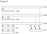
- Figure 8 illustratively shows such an optical element.
- the optical element may comprise a first diffractive light guide plate (200A), a second diffractive light guide plate (200B) and a third diffractive light guide plate (200C) sequentially.
- a first optical film (100A) may be disposed between the first diffractive light guide plate (200A) and the second diffractive light guide plate (200B).
- a second optical film (100B) may be disposed between the second diffractive light guide plate (200B) and the third diffractive light guide plate (200C).
- the first diffractive light guide plate, the second diffractive light guide plate and the third diffractive light guide plate may match blue, green and red wavelength bands, respectively.
- the first optical film may have an absorption band for blue light
- the second optical film may have absorption bands for blue and green light.
- the present invention also relates to an imaging device comprising the optical element.
- the imaging device comprises a light source and the optical element disposed on the light outgoing side of the light source.
- the optical element may allow light from the light source to reach an eye box or an observer's eye.
- the imaging device can be implemented using a transmissive scanning technique in which the light source is modulated by a white light backlight optically active material. This technique is generally implemented using an LCD-type display having a strong backlight and a high optical energy density.
- the imaging device may also be implemented using reflection techniques in which the external light is reflected and optically modulated by the active material. Depending on the technique, the lighting is illuminated from the top by either a white source or an RGB source.
- Digital light processing (hereinafter, DLP), liquid crystal on silicon (hereinafter, LCOS) and Mirasol display technologies from Qualcomm are examples of efficient, reflective technologies in which most energy is reflected from a modulation structure, which can be used in the present system.
- the imaging device may further comprise a lens between the optical element and the light source.
- the lens may direct light from the light source to the optical element.
- the lens may be a collimate lens.
- the light emitted from the light source may be unpolarized light, E-state polarized light or M-state polarized light.
- the imaging apparatus may further comprise a polarization switch between the optical element and the light source.
- the polarization switch can switch the polarization direction of all wavelength bands or some wavelength bands of the incident polarized light by 90 degrees.
- the imaging device may be a head-up display device (HUD).
- the imaging device may have an eyewear type.
- the imaging device can be used as an augmented reality apparatus.
- the imaging device can be used to display a mixture of an actual object and a virtual image in a physical environment. Such an image device can prevent the crosstalk as well as improve the diffraction efficiency by applying the optical film of the present application together with the diffractive light guide plate.
- Figure 9 illustratively shows coupling efficiency improvement and crosstalk reduction principles using the optical element of the present application.
- the first diffractive light guide plate (200A) matching the blue wavelength, the second diffractive light guide plate (200B) matching the green wavelength and the third diffractive light guide plate (200C) matching the red wavelength are sequentially disposed.
- a first optical film (100A) having an absorption band for blue light is disposed between the first diffractive light guide plate and the second diffractive light guide plate
- a second optical film (100B) having absorption bands for green light and blue light is disposed between the second diffractive light guide plate and the third diffractive light guide plate.
- the vibration direction of the M polarization state passing through the diffractive light guide plate without being coupled thereto is assumed to be 0 degree and the vibration direction of the coupled E polarization state is assumed to be 90 degrees.
- the red, green, and blue wavelengths are emitted from the light source (LCos) (300) to the 0-degree polarization state (M polarization state). While the light passes through the polarization switch (400), the red wavelength and the blue wavelength are converted into a 90-degree polarization state (E polarization state). While the red, green, and blue wavelengths pass through the first diffractive light guide plate (200A), the blue wavelength is coupled thereto. The blue wavelength can reach the eye box or the observer's eye (500) by the first diffractive light guide plate.
- the remaining blue wavelength transmitted without being coupled to the first diffractive light guide plate is absorbed by the first optical film (100A).
- the red and green wavelengths passing through the first diffractive light guide plate (200A) their polarization direction is rotated by 90 degrees by the first optical film (100A).
- the green wavelength is coupled by the second diffractive light guide plate (200B), and the red wavelength passes through the second diffractive light guide plate (200B).
- the green wavelength can reach the eye box or the observer's eye (500) by the second diffractive light guide plate.
- the remaining green wavelength and the remaining blue wavelength transmitted without being coupled to the second diffractive light guide plate (200B) are absorbed by the second optical film (100B).
- each diffractive light guide plate can couple the matched wavelength with a high coupling efficiency, thereby reducing the crosstalk.
- the imaging device comprises the optical film or the optical element of the present application
- other parts or structures, and the like are not particularly limited, where all contents known in this field can be appropriately applied.
- the optical film of the present application does not only exhibit broadband polarization conversion characteristics in the visible light region, but also has absorption bands in the visible light region.
- Such an optical film can be applied to an imaging device such as an augmented reality apparatus as an optical element such as a diffractive light guide plate laminate to suppress crosstalk.
- a pressure-sensitive adhesive layer AD701 product from LG Chemical, acrylic pressure-sensitive adhesive
- the first retardation film has a multilayer structure of a first liquid crystal layer having a half-wave phase retardation characteristic (Rin value for a wavelength of 550nm is 275nm) and an optical axis of 15 degrees relative to a reference axis (transverse direction) and a second liquid crystal layer having a quarter-wave phase retardation characteristic (Rin value for a wavelength of 550nm is 137.5nm) and an optical axis of 75 degrees relative to a reference axis (transverse direction).
- the second retardation film is prepared in the same manner as the first retardation film. In the bonding of the first and second retardation films, the second liquid crystal layers having the quarter-wave retardation characteristic were bonded so as to be in contact with the pressure-sensitive adhesive layer.
- a retardation film (polycarbonate stretched film from Teijin Company) having an R (650)/R (550) value smaller than an R (450)/R (550) value (normal dispersion characteristic) and a half-wave phase retardation characteristic was prepared as an optical film of Reference Example 2.
- a sample was prepared by attaching each optical film and a polarizing film via a 20 ⁇ m thick pressure-sensitive adhesive such that the angle between the optical axis of the optical film and the absorption axis of the polarizing film was 45 degrees.
- absorption axis transmittance and transmission axis transmittance were measured for wavelengths of 380 nm to 780 nm by a method of rotating the polarizer of the light source using a transmission spectrum measuring instrument from JASCO Co. to measure the minimum transmittance and the maximum transmittance, and the results were shown in Table 1 and Figure 10 .
- the graph (A) in Figure 10 shows the absorption axis transmittance and the graph (B) shows the transmission axis transmittance. It can be confirmed that Reference Example 1 having the reverse dispersion characteristic has polarization conversion characteristics in the entire visible light wavelength region, and has excellent characteristics as compared to Reference Example 2 having the normal dispersion characteristic.
- [Table 1] Absorption Axis Transmittance (%) Transmission Axis Transmittance (%) Wavelength (nm) Reference Example 1 Reference Example 2 Reference Example 1 Reference Example 1 Reference Example 2 455 0.51 7.39 94.87 86.77 530 0.27 0.06 98.38 94.60 625 1.48 0.09 97.45 95.08
- Figure 11 shows transmittance graphs (x-axis: wavelength [nm], y-axis: transmittance [%]) of four dyes having absorption bands in a narrow wavelength region for wavelengths.
- Dye 1, Dye 2, Dye 3 and Dye 4 are FDB005, FDB006, FDG003 and FDG007 products from Yamada Chemical, respectively.
- an acrylic resin AD701 product from LG Chemical was used as a pressure-sensitive adhesive resin.
- Figure 12 shows transmittance graphs (x-axis: wavelength [nm], y-axis: transmittance [%]) of a pressure-sensitive adhesive layer containing a dye.
- Green cut is possible using Dye 4
- Green-Blue cut is possible by mixing Dye 1, Dye 2, Dye 3 and Dye 4
- Blue cut is possible by mixing Dye 1, Dye 2 and Dye 3.
- An optical film having the structure of Figure 4 was prepared as Example 1.
- the first retardation film and the second retardation film were prepared in the same manner as in Reference Example 1.
- a pressure-sensitive adhesive layer containing the Dye 4 was used as the pressure-sensitive adhesive layer for bonding the first retardation film and the second retardation film.
- As the pressure-sensitive adhesive resin of the pressure-sensitive adhesive layer an acrylic resin (AD701 product from LG Chemical) was used, and the dye was added in an amount of about 3.5 parts by weight relative to 100 parts by weight of the pressure-sensitive adhesive resin.
- a sputter-type antireflection layer (Clear Type AR1.5 Grade from Dexerials) was applied using an inorganic low refractive (MgF 2 ) material.
- An optical film was prepared in the same manner as in Example 1, except that in the production of the optical film of Example 1, as each of the first and second antireflection layers, an antireflection layer (DSG03 Grade from DNP) was applied using a mixed material of a solution type PETA (pentaerythritol triacrylate) organic binder and hollow silica instead of the sputter-type antireflection layer.
- DSG03 Grade from DNP an antireflection layer
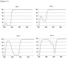
- the transmittance according to wavelengths after the light resistance test (Atlas Ci3000) at 40°C was evaluated using light having a wavelength of 420 nm at an intensity of 1.2 W/m 2 , and the results were shown in Figure 13 .
- the graph (A) in Figure 13 is a transmittance graph of Example 1
- the graph (B) is a transmittance graph of Example 2.
- An imaging device having the structure of Figure 9 is prepared. Specifically, the first diffractive light guide plate (200A) matching the blue wavelength, the second diffractive light guide plate (200B) matching the green wavelength, and the third diffractive light guide plate (200C) matching the red wavelength are sequentially disposed from the light source (LcoS) (300).
- the first optical film (100A) having an absorption band for blue light is disposed between the first diffractive light guide plate and the second diffractive light guide plate, and the second optical film (100B) having absorption bands for green light and blue light is disposed between the second diffractive light guide plate and the third diffractive light guide plate.
- a diffractive light guide plate laminate in which the first diffractive light guide plate (200A) matching the blue wavelength, the second diffractive light guide plate (200B) matching the green wavelength and the third diffractive light guide plate (200C) matching the red wavelength are disposed sequentially from the light source (LcoS) (300), is prepared as Comparative Example 1.
- the first and second optical films of Example 1 have not been disposed between the diffractive light guide plates.
- the crosstalk can be evaluated by operating the light source and measuring the intensity of light on the side where light is emitted from the diffractive light guide plate laminate.
- the RGB region shows the uniform and high light intensity (brightness)
- Comparative Example 1 the color is uneven in the RGB region and the intensity of light is also reduced.
- 10 first retardation film, 20: second retardation film, 30: color filter layer, 101, 201: first liquid crystal layer, 102, 202: second liquid crystal layer, 40: first base layer, 50: second base layer, 60: first antireflection layer, 70: second antireflection layer, 80: first barrier layer, 90: second barrier layer, 100: diffractive light guide plate, 10A: input diffraction grating, 10B: outgoing diffraction grating, 10C: substrate, 100A: first optical film, 100B: second optical film, 200A: first diffractive light guide plate, 200B: second diffractive light guide plate, 200C: third diffractive light guide plate, 300: light source, 400: polarization switch, 500: eye box (observer)
Description
- This application relates to an optical film, an optical element and an imaging device.
- Augmented reality is a process of combining or increasing useful information created by a computer, when images and photographs are displayed by computer programming, by superimposing them on images. In other words, it is a process of superimposing three-dimensional virtual objects into the real world. An example of devices using the augmented reality includes a head-up display device (HUD), which is applied to a canopy or helmet of a fighter or tank pilot so that the pilot can view terrain or features and simultaneous view various information. Recently, it can often be seen that can be applied to a vehicle as well, information such as a speed are displayed on the front window of the vehicle (Patent Document 1:
Korean Patent Laid-Open Publication No. 2016-0109021
US 2013/044286 A1 describes an optical film, a circular polarizing plate and a display device. The optical film comprises an optically anisotropic polymeric layer and a liquid crystal layer. An optical axis thereof is formed on the polymeric layer to be perpendicular to an optical axis of the polymeric layer, or to form an angle of 61.5 degrees with the optical axis of the polymeric layer. -
EP2733517 A1 discloses a head-mounted display comprising diffractive light guide plates and a half-wave plate in between for the rotation of polarization. - An imaging device such as an augmented reality apparatus may comprise a plurality of diffractive light guide plate laminates in order to allow light from a light source to reach an observer's eye. At this time, when the light of a wavelength component matched to each diffractive light guide plate is not coupled (hereinafter, may be referred to as crosstalk), it may result in reducing brightness of the light reaching the observer's eye, obtaining uneven color and deteriorating quality of the reproduced virtual image. Accordingly, there is a demand for a technique capable of reducing the crosstalk while improving the coupling efficiency of the diffractive light guide plate.
- The present invention relates to an optical element according to
claim 1, that comprises an optical film which is a means for solving the above problem. The optical film of the present application satisfiesEquation 1 below, has a half-wave phase retardation characteristic and has an absorption band in the visible light region.
- In
Equation 1 above, R (λ) is an in-plane retardation value of the optical film for light having a wavelength of λ nm. - In this specification, the in-plane retardation (Rin) value can be calculated by
Equation 2 below.
- In
Equation 2, d is a thickness of an optical film, a retardation film or a liquid crystal layer, and nx and ny are each a refractive index of the optical film, the retardation film or the liquid crystal layer in x-axis and y-axis directions. The x-axis means a direction parallel to the in-plane slow axis of the optical film, the retardation film or the liquid crystal layer, and the y-axis means a direction parallel to the in-plane fast axis of the optical film, the retardation film or the liquid crystal layer. The x-axis and the y-axis may be orthogonal to each other in the plane of the optical film. In this specification, while the in-plane retardation is described, unless otherwise specified, it means an in-plane retardation for light having a wavelength of 550 nm. - In this specification, when the term such as vertical, horizontal, orthogonal or parallel is used while defining an angle, it means substantially vertical, horizontal, orthogonal, or parallel to the extent that the desired effect is not impaired, which includes, for example, an error that takes a production error or a deviation (variation), and the like, into account. For example, each case of the foregoing may include an error within about ±15 degrees, an error within about ± 10 degrees or an error within about ±5 degrees.
- The optical film exhibits a desired phase retardation characteristic in the visible light wavelength region by satisfying
Equation 1 above. The characteristicsatisfying Equation 1 above can be referred to as a reverse wavelength dispersion characteristic. - In one example, the value of R(650)/R(550) in the optical film may be 1.01 to 1.19, 1.02 to 1.18, 1.03 to 1.17, 1.04 to 1.16, 1.05 to 1.15, 1.06 to 1.14, 1.07 to 1.13, 1.08 to 1.12 or 1.09 to 1.11. In one example, the value of R(450)/R(550) in the optical film may be 0.81 to 0.99, 0.82 to 0.98, 0.83 to 0.97, 0.84 to 0.96, 0.85 to 0.95, 0.86 to 0.94, 0.87 to 0.93, 0.88 to 0.92 or 0.89 to 0.91.
- The optical film has a half-wave phase retardation characteristic. In this specification, the term "n-wavelength phase retardation characteristic" may mean a characteristic that the incident light can be phase-delayed by n times the wavelength of the incident light within at least a part of the wavelength range. In this specification, the half-wave phase retardation characteristic may mean that the in-plane retardation value for light having a wavelength of 550 nm is 200 nm to 290 nm or 240 nm to 280 nm.
- If the optical film has a half-wave phase retardation characteristic, it can rotate the vibration direction of the incident polarized light by 90 degrees. As described below, the diffractive light guide plate can pass light in a wavelength band of a specific polarization state, where light in a wavelength band of another polarization state can be coupled into the diffractive light guide plate. The optical film can control the polarization state of the wavelength component so as to be coupled to the diffractive light guide plate. Therefore, the optical film can improve the coupling efficiency of the diffractive light guide plate and reduce the crosstalk.
- The optical film has an absorption band in the visible light wavelength region. In this specification, the visible light may mean light rays in the wavelength range of about 380 nm to 750nm. In this specification, the "absorption band" may mean a wavelength band including the wavelength of the point exhibiting the highest absorbance or the point exhibiting the lowest transmittance when the absorbance or the transmittance for wavelengths has been measured. In one example, the absorption band herein may mean a wavelength band of the point exhibiting transmittance of about 20% or less in the transmittance spectrum for wavelengths. The width of the wavelength band may be, for example, about 20 nm or more.
- In one example, the absorption band of the optical film may comprise one or more wavelength regions of a red wavelength region, a green wavelength region and a blue wavelength region. In this specification, the red wavelength region may mean about 620nm to 750nm, the green wavelength region may mean about 495nm to 570nm, and specifically, 500nm to 570nm, and the blue wavelength region may mean about 450nm to 495nm, and specifically, 450nm to 490nm. In one example, the optical film may have an absorption band in any one wavelength region among combinations of the wavelength regions, or may have an absorption band in a combination of two wavelength regions among combinations of the wavelength regions.
- As the optical film has an absorption band in the visible light wavelength region, when the optical film is used together with the diffractive light guide plate, as described below, it can absorb the residual light transmitted without being coupled to the diffractive light guide plate, thereby further suppressing the crosstalk.
- In one example, the optical film may sequentially comprise a first retardation film (10), a color filter layer (30) and a second retardation film (20), as shown in
Figure 1 . The first retardation film may satisfyEquation 1 above and have a quarter-wave phase retardation characteristic. The color filter layer may comprise a dye having an absorption band in the visible light wavelength region. The second retardation film may satisfyEquation 1 above and have a quarter-wave phase retardation characteristic. In this specification, the quarter-wave phase retardation characteristic may mean that the in-plane retardation value for light having a wavelength of 550 nm is 130nm to 200nm or 130 to 180nm or 130 to 150nm. The optical film of the present application has a vertically symmetrical structure based on the color filter layer, so that curling occurring in a thin film can be minimized. - In one example, the first retardation film and the second retardation film may have a multilayer structure comprising a first liquid crystal layer having a half-wave phase retardation characteristic and a second liquid crystal layer having a quarter-wave phase retardation characteristic. Such a multilayer structure can be advantageous for realizing the broadband phase retardation characteristic.
-
Figure 2 illustratively shows an optical film sequentially comprising a first retardation film including a first liquid crystal layer (101) and a second liquid crystal layer (102), a color filter layer (30) and a second retardation film including a first liquid crystal layer (201) and a second liquid crystal layer (202). - In one example, the optical axis of the first retardation film and the optical axis of the second retardation film may be parallel to each other. Accordingly, the optical film can be advantageous for realizing the half-wave phase retardation characteristic as the sum of the phase retardation characteristics of the first retardation film and the second retardation film.
- Hereinafter, while the first liquid crystal layer and the second liquid crystal layer are described, unless otherwise specified, the description can be commonly applied to the first liquid crystal layer and the second liquid crystal layer included in the first retardation film and the second retardation film, respectively.
- In one example, the second liquid crystal layer may be disposed closer to the color filter layer than the first liquid crystal layer. Through this structure, the optical film can be advantageous for realizing the half-wave phase retardation characteristic.
- In one example, the optical axis of the first liquid crystal layer and the optical axis of the second liquid crystal layer may form 55 degrees to 65 degrees, 57 degrees to 63 degrees or 59 degrees to 61 degrees to each other. Accordingly, it may be more advantageous to realize a retardation
film satisfying Equation 1 above and having a quarter-wave phase retardation characteristic. - In one example, the optical axis of the first liquid crystal layer may form 12.5 degrees to 17.5 degrees and the optical axis of the second liquid crystal layer may form 72.5 degrees to 77.5 degrees, based on the transverse direction (TD, direction orthogonal to the mechanical flow direction) or the longitudinal direction (MD; mechanical direction, mechanical flow direction). Accordingly, it may be more advantageous to realize a retardation
film satisfying Equation 1 above and having a quarter-wave phase retardation characteristic. In one example, the longitudinal direction may mean the longitudinal direction of the optical film, and the transverse direction may mean the width direction of the optical film. - In one example, each of the first and second liquid crystal layers may have a reverse wavelength dispersion characteristic, a normal wavelength dispersion characteristic, or a flat wavelength dispersion characteristic. In this specification, the reverse wavelength dispersion characteristic may mean a characteristic that satisfies
Equation 1 above. The normal wavelength dispersion characteristic may mean a characteristic that satisfiesEquation 3 below, and the flat wavelength dispersion characteristic may mean a characteristic that satisfiesEquation 4 below.

- In
Equations - The first and second liquid crystal layers may each comprise a liquid crystal compound. The liquid crystal compound may be a polymerizable liquid crystal compound. In one example, the first and second liquid crystal layers may comprise the polymerizable liquid crystal compound in a polymerized form. In this specification, the term "polymerizable liquid crystal compound" may mean a compound containing a moiety capable of exhibiting liquid crystallinity, such as a mesogen skeleton, and also containing one or more polymerizable functional groups. In addition, the phrase "a polymerizable liquid crystal compound is contained in a polymerized form" may mean a state where the liquid crystal compound is polymerized to form a skeleton such as a main chain or a side chain of the liquid crystal polymer in the liquid crystal layer. In one example, the first liquid crystal layer and the second liquid crystal layer may each comprise the liquid crystal compound in a horizontally oriented state.
- The first and second liquid crystal layers may each comprise a polymerizable liquid crystal compound in a non-polymerized state or may further comprise known additives such as a polymerizable non-liquid crystal compound, a stabilizer, a non-polymerizable non-liquid crystal compound or an initiator.
- In one example, the first liquid crystal layer and the second liquid crystal layer may each have a difference between a refractive index in a plane slow axis direction and a refractive index in a plane fast axis direction in a range of 0.05 to 0.2, 0.07 to 0.2, 0.09 to 0.2 or 0.1 to 0.2. Here, the refractive index in the plane slow axis direction may mean the refractive index in the direction showing the highest refractive index in the plane of the liquid crystal layer, and the refractive index in the fast axis direction may mean the refractive index in the direction showing the lowest refractive index on the plane of the liquid crystal layer. Generally, in an optically anisotropic liquid crystal layer, the fast axis and the slow axis are formed in directions perpendicular to each other. Each of the refractive indices may be a refractive index measured for light having a wavelength of 550 nm or 589 nm. For example, using Axoscan from Axomatrix, the refractive index difference can be measured according to the manufacturer's manual.
- In one example, the first and second liquid crystal layers may each have a thickness of about 0.5µm to 2.0µm or about 0.5µm to 1.5µm.
- The liquid crystal layer having the relationship of the refractive indices and the thickness can realize the phase retardation characteristic suitable for the application to be applied.
- Each of the first and second retardation films may be formed by a method of coating a second liquid crystal layer on a first liquid crystal layer. The first liquid crystal layer may be formed by a method of coating a first liquid crystal layer on a base layer to be described below.
- The color filter layer may be a pressure-sensitive adhesive layer containing the dye and a pressure-sensitive adhesive resin. The content of the dye can be suitably controlled in consideration of the absorption band and tackiness, and the like of the color filter layer required in the present application. The content of the dye may be included, for example, in a range of 0.5 to 20 parts by weight relative to 100 parts by weight of the pressure-sensitive adhesive resin. Specifically, the dye may be contained in a ratio of 0.5 parts by weight or more, 1 part by weight or more, or 2 parts by weight or more, and may be contained in a ratio of 20 parts by weight or less, 10 parts by weight or less, 7.5 parts by weight or less, or 5 parts by weight or less, relative to 100 parts by weight of the pressure-sensitive adhesive resin. As it is used in a diffractive light guide plate laminate within such a content range, it is possible to be suitable for reducing the crosstalk.
- As the dye, one or more dyes selected from the group consisting of anthraquinone dyes, methine dyes, azomethine dyes, oxazine dyes, azo dyes, styryl dyes, coumarin dyes, porphyrin dyes, dibenzofuranone dyes, diketopyrrolopyrrole dyes, rhodamine dyes, xanthene dyes and pyrromethene dyes can be used.
- The dye may have an absorption band or absorption peak in the visible light wavelength region. In this specification, the absorption peak may mean the wavelength of the point exhibiting the highest absorbance or the point exhibiting the lowest transmittance when the absorbance or the transmittance for wavelengths has been measured. The absorption band or the absorption peak of the dye may be included in the absorption band of the optical film or the color filter layer.
- As the dye contained in the color filter layer, a single dye or a mixed dye may be used. In one example, in the optical film or color filter layer, if absorption bands in a somewhat broad wavelength region are required, a mixture of a plurality of dyes having absorption bands in a narrow wavelength region may also be used. The pressure-sensitive adhesive resin may include one or more selected from the group consisting of an acrylic resin, a silicone resin, an ester resin, a urethane resin, an amide resin, an ether resin, a fluorine resin and a rubber resin.
- The pressure-sensitive adhesive layer may have a thickness of 7µm to 30µm. When the thickness range of the pressure-sensitive adhesive layer is within the above range, it may be advantageous from the viewpoint of attachment reliability between films.
- In one example, the optical film may be produced by attaching the first retardation film and the second retardation film via the pressure-sensitive adhesive layer.
- The optical film may further comprise a base layer. In one example, as shown in
Figure 3 , the optical film may further comprise a first base layer (40) and a second base layer (50) on the outer sides of the first retardation film (10) and the second retardation film (20), respectively. In this specification, the "outer side" may mean the opposite side of the side where the color filter layer is present. - As the base layer, a film base material may be used. As the base layer, a base material having optical transparency may be used. As the base layer, a base layer that the in-plane retardation value is adjusted so as to minimize the influence on polarization may be used. In one example, as the base layer, an isotropic film may be used. In this specification, the isotropy may mean a characteristic in which the in-plane retardation value is 10nm or less. As the isotropic film, a PC (polycarbonate) film, a TAC (triacetyl cellulose) film or a COP (cycloolefin copolymer) film, and the like may be used. In another example, as the base layer, a super retardation film (SRF) may be used. Such an SRF may have an in-plane retardation value of about 1000 nm or more. As such an SRF, a PET (polyethyleneterephtalate) film may be used. In one example, if the isotropic film or super retardation film comprises a UV additive, it may be advantageous for reliability.
- The optical film may further comprise an antireflection layer. In one example, the optical film may further comprise a first antireflection layer and a second antireflection layer on the outer sides of the first retardation film and the second retardation film, respectively. When the optical film further comprises other layers such as a base layer on the outer sides of the first retardation film and the second retardation film, the first antireflection layer and the second antireflection layer may exist at the outermost sides of the optical film.
Figure 4 illustratively shows an optical film comprising a first antireflection layer (60) and a second antireflection layer (70) on the outermost sides of the optical film ofFigure 3 . - The optical film can improve the transmittance of the optical film through the antireflection layer. In one example, the antireflection layer can be produced by a wet coating method or a deposition method. As described below, when the optical film further comprises a barrier layer, it may be advantageous to use an antireflection layer of a deposition method in terms of improving the transmittance.
- As the antireflection layer, a low refractive layer may be used. As a material of the antireflection layer suitable for the deposition method, for example, a low refractive inorganic material may be used. As the low refractive inorganic material, a material having a refractive index of about 1.45 or less, or 1.40 or less for a wavelength of 550nm may be used. The low refractive inorganic material can be exemplified by, for example, metal fluoride and the like. A specific example of the metal fluoride can be exemplified by magnesium fluoride (MgF2) and the like. The material of the antireflection layer suitable for the wet coating method (solution method) may be, for example, a mixture of an organic binder and low refractive particles. As the organic binder, a (co)polymer of a photopolymerizable compound can be used, where a specific example thereof can be exemplified by an acrylic resin. As the low refractive particles, particles having a refractive index of about 1.45 or less, or 1.40 or less for a wavelength of 550nm can be used. The low refractive particles can be exemplified by hollow silica, mesoporous silica, and the like.
- The optical film may further comprise a barrier layer. In one example, the optical film may comprise a first barrier layer on one side of the first retardation film and may comprise a second barrier layer on one side of the second retardation film. In one specific example, as shown in
Figure 5 , the optical film may comprise a first barrier layer (80) between the first retardation film (10) and the color filter layer (30), and may further comprise a second barrier layer (90) between the second retardation film (20) and the color filter layer (30). In another specific example, as shown inFigure 6 , the optical film may comprise a first barrier layer (80) on the outer side of the first retardation film (10), and may further comprise a second barrier layer (90) of the second retardation film. At this time, when the optical film further comprises other layers such as a base layer on the outer sides of the first retardation film and the second retardation film, the first barrier layer and the second barrier layer may be disposed more adjacent to the first retardation film and the second retardation film than other layers. - The optical film can improve light resistance through the barrier layer. For example, the dye can react with oxygen in the air to cause degradation, where the occurrence of degradation can be reduced through the barrier layer. As the barrier layer, a gas barrier layer can be used.
- As the barrier layer, a layer having a function of preventing permeation of oxygen, moisture, nitrogen oxide, sulfur oxide or ozone in the atmosphere can be used. As the material of the barrier layer, a material having a function of preventing substances, such as moisture and oxygen, which promote degradation of an element from entering the element can be appropriately selected and used.
- In one example, the barrier layer may comprise a metal such as In, Sn, Pb, Au, Cu, Ag, Al, Ti and Ni; a metal oxide such as TiO, TiO2, Ti3O3, Al2O3, MgO, SiO, SiO2, GeO, NiO, CaO, BaO, Fe2O3, Y2O3, ZrO2, Nb2O3 and CeO2; a metal nitride such as SiN; a metal oxynitride such as SiON; a metal fluoride such as MgF2, LiF, AlF3 and CaF2; a polymer such as polyacrylate, polyethylene, polypropylene, polyimide, polyurea, polytetrafluoroethylene, polychlorotrifluoroethylene or polydichlorodifluoroethylene, or a copolymer of chlorotrifluoroethylene and dichlorodifluoroethylene; a copolymer obtained by copolymerizing tetrafluoroethylene with a comonomer mixture comprising at least one comonomer; a fluorine-containing copolymer having a cyclic structure in a copolymerized main chain; an absorbent material having an absorption rate of 1% or more; and a moistureproof material having an absorption coefficient of 0.1% or less.
- In one example, the barrier layer may be a single-layer structure or a multi-layer structure. The single-layer structure may comprise, for example, one barrier layer material, or may also comprise a mixture of two or more barrier layer materials. When the optical film comprises the barrier layer, the transmittance is lowered due to the light absorption and the refractive index mismatch, whereby the performance may be deteriorated. In this case, when the antireflection layer by a deposition method having a high coating film density, for example, a sputter method is applied, the light resistance can be improved without lowering the transmittance. The film comprising the antireflection layer may have a water vapor transmission rate (WVTR) of, for example, 1 g/m2/day or less.
- The present invention relates to an optical element comprising the optical film. According to the invention, the optical element comprises at least two diffractive light guide plates sequentially, and comprises the optical film between the at least two diffractive light guide plates. The two diffractive light guide plates may be laminated in a superposed state. Therefore, the light that has passed through any one diffractive light guide plate of at least two diffractive light guide plates after being incident thereon can be incident on the remaining diffractive light guide plate.
- In this specification, the diffractive light guide plate may mean a light guide plate comprising a plurality of diffractive optical elements (DOEs). The diffractive light guide plate may be formed of a thin flat sheet of plastic or glass. In this specification, the diffractive optical element may mean an element using diffraction by periodic structures. The diffractive optical element may be abbreviated as a diffraction grating or DOE.
-
Figure 7 illustratively shows the structure of the diffractive light guide plate (100) and the total internal reflection of the wavelength band λ1 (indicated by the arrow) coupled to the inside or outside of the diffractive light guide plate. The diffractive light guide plate (100) may comprise two or more diffraction gratings, such as an input diffraction grating (10A) coupling light rays into the diffractive light guide plate and an outgoing diffraction grating (10B) diffracting the light rays out of the diffractive light guide plate. InFigure 7 , the diffraction gratings (10A, 10B) have been shown as transmissive diffraction gratings attached inside the lower surface of the substrate (10C) of the diffractive light guide plate. - The light rays of the wavelength band λ1 from the light source (300) can be collimated through a lens or the like and can be coupled to the substrate (10C) by the input diffraction grating (10A) at an incident angle θ1. The input diffraction grating (10A) can redirect the wavelength band to a diffraction angle θ2. The refractive index n2, the incident angle θ1 and the diffraction angle θ2 can be controlled so that the light rays of the wavelength band λ1 are subjected to internal total reflection within the substrate (10C). The light rays of the wavelength band λ1 can be reflected on the surface of the substrate (10C) until they reach the outgoing diffraction grating (10B) and the light rays of the wavelength band λ1 can be diffracted from the substrate (10C) toward the eye box (500).
- The DOE of the diffractive light guide plate is sensitive to optical polarization. Therefore, by selectively controlling the polarized light of the wavelength band entering the DOE of the diffractive light guide plate, the wavelength band matched to the diffractive light guide plate can be coupled to the DOE with high efficiency. On the other hand, unmatched wavelength bands can pass through the diffractive light guide plate with a large width or in a wholly unaffected manner. Although an example using the DOE is described here, it is understood that the diffractive light guide plate may comprise other types of periodic structures of holograms, surface relief gratings or optical elements as well as the DOE. Such a structure may be referred to as an "optical grating."
- The diffractive light guide plate may be matched or optimized to a specific wavelength band. The relation is determined according to a lattice equation of the following
Equation 5.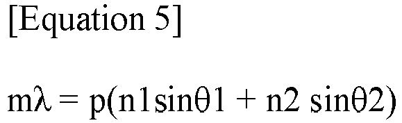
- Here, m means a diffraction order, λ means a wavelength band matched with a light guide plate or a diffraction grating, p means a lattice period, n1 means a refractive index of an incident medium, n2 means a refractive index of a light guide plate, θ1 means an incident angle, and θ2 means a diffraction angle.
- The specific diffractive light guide plate comprising the input diffraction grating and the outgoing diffraction grating can be matched to a specific wavelength band by varying parameters such as the grating period p and the refractive index n2 of the light guide plate. That is, a specific wavelength band can be coupled to the matched diffractive light guide plate having a higher coupling efficiency than other wavelength bands.
- The polarized light of the light incident on the diffraction grating can be defined by the direction of its electromagnetic field with respect to the incident plane. The plane can be defined by a lattice normal vector, and a propagation vector from an irradiation light source. The propagation vector is a K-vector scan of the light on the diffractive light guide plate. The lattice vector is a vector in the plane of the diffraction grating that defines the direction of the lattice line. As used herein, the term "E state" refers to a polarization state in which the electric field component of the wavelength band is zero along the lattice vector. As used herein, the term "M state" refers to a polarization state where the magnetic field component is zero along the lattice vector. The polarized light of the wavelength band incident on the diffraction grating of the diffractive light guide plate is controlled and changed between the E state and the M state. In one example, the wavelength band of the polarized M state incident on the diffraction grating passes through the light guide plate including the diffraction grating, whereas the wavelength band of the polarized E state incident on the diffraction grating is coupled into the light guide plate including the diffraction grating. The coupling or diffraction principle of the diffractive light guide plate is known, which may be referenced to the contents disclosed in
Korean Patent Laid-Open Publication No. 2015-0071612 - In one example, the at least two diffractive light guide plates may be different from each other in wavelength bands to be coupled (or matched). The wavelength bands different from each other may be present in the visible light region.
- In one example, the absorption band of the optical film and the coupled wavelength band of any one diffractive light guide plate among the at least two diffractive light guide plates may have a region overlapping each other. The absorption band of the optical film may have a region overlapping each other with the wavelength band coupled to the diffractive light guide plate adjacent to the optical film among the at least two diffractive light guide plates.
- In one specific example, the absorption band of the optical film may have a region overlapping each other with the coupling wavelength band of the nearest diffractive light guide plate through which light is transmitted to the optical film side. Through this, the optical film can absorb the remaining light that is not coupled in the diffractive light guide plate and is transmitted, so that the crosstalk can be further suppressed.
- In addition, it may be preferable that the absorption band of the optical film does not have a region overlapping each other with the coupling wavelength band of the nearest diffractive light guide plate through which the light passing through the optical film is incident. This is because the intensity of the light rays reaching the observer's eye may be weakened when absorbing the light rays in the wavelength region to be coupled to the diffractive light guide plate.
- In one example, the optical element may comprise at least three diffractive light guide plates, and may comprise at least two optical films disposed between the at least three diffractive light guide plates.
Figure 8 illustratively shows such an optical element. The optical element may comprise a first diffractive light guide plate (200A), a second diffractive light guide plate (200B) and a third diffractive light guide plate (200C) sequentially. A first optical film (100A) may be disposed between the first diffractive light guide plate (200A) and the second diffractive light guide plate (200B). A second optical film (100B) may be disposed between the second diffractive light guide plate (200B) and the third diffractive light guide plate (200C). In one example, the first diffractive light guide plate, the second diffractive light guide plate and the third diffractive light guide plate may match blue, green and red wavelength bands, respectively. At this time, when the light from the light source is first incident on the first diffractive light guide plate, the first optical film may have an absorption band for blue light, and the second optical film may have absorption bands for blue and green light. - The present invention also relates to an imaging device comprising the optical element. The imaging device comprises a light source and the optical element disposed on the light outgoing side of the light source. The optical element may allow light from the light source to reach an eye box or an observer's eye.
- There are a variety of image generation techniques that can be used to implement the imaging device. The imaging device can be implemented using a transmissive scanning technique in which the light source is modulated by a white light backlight optically active material. This technique is generally implemented using an LCD-type display having a strong backlight and a high optical energy density. The imaging device may also be implemented using reflection techniques in which the external light is reflected and optically modulated by the active material. Depending on the technique, the lighting is illuminated from the top by either a white source or an RGB source. Digital light processing (hereinafter, DLP), liquid crystal on silicon (hereinafter, LCOS) and Mirasol display technologies from Qualcomm are examples of efficient, reflective technologies in which most energy is reflected from a modulation structure, which can be used in the present system.
- The imaging device may further comprise a lens between the optical element and the light source. The lens may direct light from the light source to the optical element. The lens may be a collimate lens.
- The light emitted from the light source may be unpolarized light, E-state polarized light or M-state polarized light. The imaging apparatus may further comprise a polarization switch between the optical element and the light source. The polarization switch can switch the polarization direction of all wavelength bands or some wavelength bands of the incident polarized light by 90 degrees.
- In one example, the imaging device may be a head-up display device (HUD). The imaging device may have an eyewear type. In one example, the imaging device can be used as an augmented reality apparatus. The imaging device can be used to display a mixture of an actual object and a virtual image in a physical environment. Such an image device can prevent the crosstalk as well as improve the diffraction efficiency by applying the optical film of the present application together with the diffractive light guide plate.
-
Figure 9 illustratively shows coupling efficiency improvement and crosstalk reduction principles using the optical element of the present application. Sequentially from the light source (LcoS) (300), the first diffractive light guide plate (200A) matching the blue wavelength, the second diffractive light guide plate (200B) matching the green wavelength and the third diffractive light guide plate (200C) matching the red wavelength are sequentially disposed. A first optical film (100A) having an absorption band for blue light is disposed between the first diffractive light guide plate and the second diffractive light guide plate, and a second optical film (100B) having absorption bands for green light and blue light is disposed between the second diffractive light guide plate and the third diffractive light guide plate. - The vibration direction of the M polarization state passing through the diffractive light guide plate without being coupled thereto is assumed to be 0 degree and the vibration direction of the coupled E polarization state is assumed to be 90 degrees. The red, green, and blue wavelengths are emitted from the light source (LCos) (300) to the 0-degree polarization state (M polarization state). While the light passes through the polarization switch (400), the red wavelength and the blue wavelength are converted into a 90-degree polarization state (E polarization state). While the red, green, and blue wavelengths pass through the first diffractive light guide plate (200A), the blue wavelength is coupled thereto. The blue wavelength can reach the eye box or the observer's eye (500) by the first diffractive light guide plate. The remaining blue wavelength transmitted without being coupled to the first diffractive light guide plate is absorbed by the first optical film (100A). In the red and green wavelengths passing through the first diffractive light guide plate (200A), their polarization direction is rotated by 90 degrees by the first optical film (100A). Then, the green wavelength is coupled by the second diffractive light guide plate (200B), and the red wavelength passes through the second diffractive light guide plate (200B). The green wavelength can reach the eye box or the observer's eye (500) by the second diffractive light guide plate. Thereafter, the remaining green wavelength and the remaining blue wavelength transmitted without being coupled to the second diffractive light guide plate (200B) are absorbed by the second optical film (100B). In the red wavelength, its polarization direction is rotated by 90 degrees by the second optical film (100B). Thereafter, the red wavelength is coupled to the third diffractive light guide plate (200C). The red wavelength can reach the eye box or the observer's eye (500) by the third diffractive light guide plate. Thus, through the optical film of the present application, each diffractive light guide plate can couple the matched wavelength with a high coupling efficiency, thereby reducing the crosstalk.
- As long as the imaging device comprises the optical film or the optical element of the present application, other parts or structures, and the like are not particularly limited, where all contents known in this field can be appropriately applied.
- The optical film of the present application does not only exhibit broadband polarization conversion characteristics in the visible light region, but also has absorption bands in the visible light region. Such an optical film can be applied to an imaging device such as an augmented reality apparatus as an optical element such as a diffractive light guide plate laminate to suppress crosstalk.
-
-
Figure 1 illustratively shows an optical film of the present application. -
Figure 2 illustratively shows an optical film of the present application. -
Figure 3 illustratively shows an optical film of the present application. -
Figure 4 illustratively shows an optical film of the present application. -
Figure 5 illustratively shows an optical film of the present application. -
Figure 6 illustratively shows an optical film of the present application. -
Figure 7 illustratively shows the structure of the diffractive light guide plate and the total internal reflection of the light rays coupled to the inside or outside of the diffractive light guide plate. -
Figure 8 illustratively shows an optical element of the present application. -
Figure 9 illustratively shows coupling efficiency improvement and crosstalk reduction principles using an optical element of the present application. -
Figure 10 is absorption axis transmittance (A) and transmission axis transmittance (B) graphs of Reference Example 1 and Reference Example 2 for wavelengths. -
Figure 11 is transmittance graphs of four dyes having different absorption bands for wavelengths. -
Figure 12 is transmittance graphs of a pressure-sensitive adhesive layer containing a dye for wavelengths. -
Figure 13 is transmittance graphs of Example 1(A) and Example 2(B) for wavelengths after light resistance tests. - Hereinafter, the present application will be specifically described by way of examples, but the scope of the present application is not limited by the following examples.
- An optical film having a structure, in which first and second retardation films having an R(650)/R(550) value larger than an R(450)/R(550) value (reverse dispersion characteristic) and a quarter-wave phase retardation characteristic were bonded together by a pressure-sensitive adhesive layer (AD701 product from LG Chemical, acrylic pressure-sensitive adhesive) such that their optical axes were parallel to each other, was prepared. Specifically, the first retardation film has a multilayer structure of a first liquid crystal layer having a half-wave phase retardation characteristic (Rin value for a wavelength of 550nm is 275nm) and an optical axis of 15 degrees relative to a reference axis (transverse direction) and a second liquid crystal layer having a quarter-wave phase retardation characteristic (Rin value for a wavelength of 550nm is 137.5nm) and an optical axis of 75 degrees relative to a reference axis (transverse direction). The second retardation film is prepared in the same manner as the first retardation film. In the bonding of the first and second retardation films, the second liquid crystal layers having the quarter-wave retardation characteristic were bonded so as to be in contact with the pressure-sensitive adhesive layer.
- A retardation film (polycarbonate stretched film from Teijin Company) having an R (650)/R (550) value smaller than an R (450)/R (550) value (normal dispersion characteristic) and a half-wave phase retardation characteristic was prepared as an optical film of Reference Example 2.
- For the optical films each prepared in Referential Example 1 and Reference Example 2, a sample was prepared by attaching each optical film and a polarizing film via a 20µm thick pressure-sensitive adhesive such that the angle between the optical axis of the optical film and the absorption axis of the polarizing film was 45 degrees. For the sample, absorption axis transmittance and transmission axis transmittance were measured for wavelengths of 380 nm to 780 nm by a method of rotating the polarizer of the light source using a transmission spectrum measuring instrument from JASCO Co. to measure the minimum transmittance and the maximum transmittance, and the results were shown in Table 1 and
Figure 10 . The graph (A) inFigure 10 shows the absorption axis transmittance and the graph (B) shows the transmission axis transmittance. It can be confirmed that Reference Example 1 having the reverse dispersion characteristic has polarization conversion characteristics in the entire visible light wavelength region, and has excellent characteristics as compared to Reference Example 2 having the normal dispersion characteristic.[Table 1] Absorption Axis Transmittance (%) Transmission Axis Transmittance (%) Wavelength (nm) Reference Example 1 Reference Example 2 Reference Example 1 Reference Example 2 455 0.51 7.39 94.87 86.77 530 0.27 0.06 98.38 94.60 625 1.48 0.09 97.45 95.08 - Visible light absorption characteristics of the pressure-sensitive adhesive layer containing a dye were evaluated.
-
Figure 11 shows transmittance graphs (x-axis: wavelength [nm], y-axis: transmittance [%]) of four dyes having absorption bands in a narrow wavelength region for wavelengths.Dye 1,Dye 2,Dye 3 andDye 4 are FDB005, FDB006, FDG003 and FDG007 products from Yamada Chemical, respectively. In the pressure-sensitive adhesive layer, an acrylic resin (AD701 product from LG Chemical) was used as a pressure-sensitive adhesive resin. -
Figure 12 shows transmittance graphs (x-axis: wavelength [nm], y-axis: transmittance [%]) of a pressure-sensitive adhesive layer containing a dye. As shown inFigure 12 , Green cut is possible usingDye 4, Green-Blue cut is possible by mixingDye 1,Dye 2,Dye 3 andDye 4, and Blue cut is possible by mixingDye 1,Dye 2 andDye 3. - An optical film having the structure of
Figure 4 was prepared as Example 1. The first retardation film and the second retardation film were prepared in the same manner as in Reference Example 1. However, a pressure-sensitive adhesive layer containing theDye 4 was used as the pressure-sensitive adhesive layer for bonding the first retardation film and the second retardation film. As the pressure-sensitive adhesive resin of the pressure-sensitive adhesive layer, an acrylic resin (AD701 product from LG Chemical) was used, and the dye was added in an amount of about 3.5 parts by weight relative to 100 parts by weight of the pressure-sensitive adhesive resin. As each of the first and second antireflection layers, a sputter-type antireflection layer (Clear Type AR1.5 Grade from Dexerials) was applied using an inorganic low refractive (MgF2) material. - An optical film was prepared in the same manner as in Example 1, except that in the production of the optical film of Example 1, as each of the first and second antireflection layers, an antireflection layer (DSG03 Grade from DNP) was applied using a mixed material of a solution type PETA (pentaerythritol triacrylate) organic binder and hollow silica instead of the sputter-type antireflection layer.
- For Examples 1 and 2, the transmittance according to wavelengths after the light resistance test (Atlas Ci3000) at 40°C was evaluated using light having a wavelength of 420 nm at an intensity of 1.2 W/m2, and the results were shown in
Figure 13 . The graph (A) inFigure 13 is a transmittance graph of Example 1, and the graph (B) is a transmittance graph of Example 2. When the sputter-type antireflection layer having a high coating film density is used as in Example 1, it can be confirmed that the light resistance can be improved without lowering the transmittance after the light resistance test for 100 hours relative to the beginning, as compared to the case of using the antireflection layer by the wet coating method as in Example 2. - An imaging device having the structure of
Figure 9 is prepared. Specifically, the first diffractive light guide plate (200A) matching the blue wavelength, the second diffractive light guide plate (200B) matching the green wavelength, and the third diffractive light guide plate (200C) matching the red wavelength are sequentially disposed from the light source (LcoS) (300). The first optical film (100A) having an absorption band for blue light is disposed between the first diffractive light guide plate and the second diffractive light guide plate, and the second optical film (100B) having absorption bands for green light and blue light is disposed between the second diffractive light guide plate and the third diffractive light guide plate. - A diffractive light guide plate laminate, in which the first diffractive light guide plate (200A) matching the blue wavelength, the second diffractive light guide plate (200B) matching the green wavelength and the third diffractive light guide plate (200C) matching the red wavelength are disposed sequentially from the light source (LcoS) (300), is prepared as Comparative Example 1. However, the first and second optical films of Example 1 have not been disposed between the diffractive light guide plates.
- The crosstalk can be evaluated by operating the light source and measuring the intensity of light on the side where light is emitted from the diffractive light guide plate laminate. In Example 3, the RGB region shows the uniform and high light intensity (brightness), whereas in Comparative Example 1, the color is uneven in the RGB region and the intensity of light is also reduced.
- 10: first retardation film, 20: second retardation film, 30: color filter layer, 101, 201: first liquid crystal layer, 102, 202: second liquid crystal layer, 40: first base layer, 50: second base layer, 60: first antireflection layer, 70: second antireflection layer, 80: first barrier layer, 90: second barrier layer, 100: diffractive light guide plate, 10A: input diffraction grating, 10B: outgoing diffraction grating, 10C: substrate, 100A: first optical film, 100B: second optical film, 200A: first diffractive light guide plate, 200B: second diffractive light guide plate, 200C: third diffractive light guide plate, 300: light source, 400: polarization switch, 500: eye box (observer)
Claims (14)
- An optical element, comprising:at least two diffractive light guide plates (200A, 200B, 200C) sequentially; andan optical film (100A, 100B) disposed between the at least two diffractive light guide plates (200A, 200B, 200C),wherein the optical film (100A, 100B) satisfies Equation 1 below, has a half-wave phase retardation characteristic and has an absorption band in the visible light wavelength region:
 wherein, R (λ) is an in-plane retardation value of the optical film (100A, 100B) for light having a wavelength of λ nm.
 - The optical element according to claim 1, wherein the R(650)/R(550) value of the optical film (100A, 100B) is 1.01 to 1.19, and the R(450)/R(550) value of the optical film is 0.81 to 0.99.
- The optical element according to claim 1, wherein the optical film (100A, 100B) comprises a first retardation film (10) satisfying Equation 1 and having a quarter-wave phase retardation characteristic, a color filter layer (30) including a dye having an absorption band in the visible light wavelength region and a second retardation film (20) satisfying Equation 1 and having a quarter-wave phase retardation characteristic sequentially.
- The optical element according to claim 3, wherein the optical axis of the first retardation film (10) and the optical axis of the second retardation film (20) are parallel to each other.
- The optical element according to claim 3, wherein the first retardation film (10) and the second retardation film (20) each comprise a multilayer structure including a first liquid crystal layer (101, 201) having a half-wave phase retardation characteristic and a second liquid crystal layer (102, 202) having a quarter-wave phase retardation characteristic.
- The optical element according to claim 5, wherein the second liquid crystal layer (102, 202) is disposed closer to the color filter layer (30) than the first liquid crystal layer (101, 201).
- The optical element according to claim 5, wherein the optical axis of the first liquid crystal layer (101, 201) and the optical axis of the second liquid crystal layer (102, 202) form 55 degrees to 65 degrees from each other.
- The optical element according to claim 5, wherein the optical axis of the first liquid crystal layer (101, 201) forms 12.5 degrees to 17.5 degrees and the optical axis of the second liquid crystal layer (102, 202) forms 72.5 degrees to 77.5 degrees, based on a width direction of the optical film (100A, 100B) or the longitudinal direction of the optical film (100A, 100B).
- The optical element according to claim 3, wherein the color filter layer (30) is a pressure-sensitive adhesive layer comprising the dye and a pressure-sensitive adhesive resin.
- The optical element according to claim 3, wherein the optical film (100A, 100B) further comprises a first base layer (40) and a second base layer (50) on the outer sides of the first retardation film (10) and the second retardation film (20), respectively.
- The optical element according to claim 3, wherein the optical film (100A, 100B) further comprises a first antireflection layer (60) and a second antireflection layer (70) on the outer sides of the first retardation film (10) and the second retardation film (20), respectively.
- The optical element according to claim 1, wherein the at least two diffractive light guide plates (200A, 200B, 200C) have different wavelength bands of light to be coupled.
- The optical element according to claim 1, wherein the absorption band of the optical film (100A, 100B) and the wavelength band of the light coupled to the diffractive light guide plate (200A, 200B, 200C) adjacent to the optical film (100A, 100B) have a region overlapping each other.
- An imaging device comprising a light source (300) and the optical element of claim 1 disposed on the light outgoing side of the light source (300).
Applications Claiming Priority (2)
| Application Number | Priority Date | Filing Date | Title |
|---|---|---|---|
| KR20170124103 | 2017-09-26 | ||
| PCT/KR2018/011305 WO2019066429A1 (en) | 2017-09-26 | 2018-09-21 | Optical film, optical element, and imaging device |
Publications (3)
| Publication Number | Publication Date |
|---|---|
| EP3690505A1 EP3690505A1 (en) | 2020-08-05 |
| EP3690505A4 EP3690505A4 (en) | 2020-10-28 |
| EP3690505B1 true EP3690505B1 (en) | 2024-03-06 |
Family
ID=65903043
Family Applications (1)
| Application Number | Title | Priority Date | Filing Date |
|---|---|---|---|
| EP18860255.1A Active EP3690505B1 (en) | 2017-09-26 | 2018-09-21 | Optical element, and imaging device |
Country Status (7)
| Country | Link |
|---|---|
| US (1) | US11366259B2 (en) |
| EP (1) | EP3690505B1 (en) |
| JP (1) | JP6943509B2 (en) |
| KR (1) | KR102062828B1 (en) |
| CN (1) | CN111051936B (en) |
| TW (1) | TWI685682B (en) |
| WO (1) | WO2019066429A1 (en) |
Families Citing this family (2)
| Publication number | Priority date | Publication date | Assignee | Title |
|---|---|---|---|---|
| CN109727317B (en) * | 2019-01-07 | 2021-02-09 | 京东方科技集团股份有限公司 | Augmented reality system and control method |
| FR3124114A1 (en) * | 2021-06-18 | 2022-12-23 | Saint-Gobain Glass France | GLAZING COMPRISING A FUNCTIONAL COATING AND AN ABSORBENT ELEMENT FOR COLORIMETRIC ADJUSTMENT |
Citations (1)
| Publication number | Priority date | Publication date | Assignee | Title |
|---|---|---|---|---|
| US20160116739A1 (en) * | 2014-09-29 | 2016-04-28 | Magic Leap, Inc. | Architectures and methods for outputting different wavelength light out of waveguides |
Family Cites Families (37)
| Publication number | Priority date | Publication date | Assignee | Title |
|---|---|---|---|---|
| JPH0743634A (en) * | 1993-05-14 | 1995-02-14 | Olympus Optical Co Ltd | Face or head mounted display device |
| WO2003014820A1 (en) | 2001-08-03 | 2003-02-20 | Koninklijke Philips Electronics N.V. | Reflective liquid-crystal display |
| JP2003195036A (en) | 2001-12-25 | 2003-07-09 | Fuji Photo Film Co Ltd | Polarizing plate, method for manufacturing the same and liquid crystal display device |
| WO2005012990A1 (en) * | 2003-08-02 | 2005-02-10 | Advue Co., Ltd. | Patterned optical retarder and method for manufacturing the same |
| US20070264499A1 (en) | 2004-02-23 | 2007-11-15 | Lg Chem, Ltd. | Adhesive film functionalizing color compensation and near infrared ray (NIR) blocking and plasma display panel filter using the same |
| TWI251103B (en) * | 2004-02-27 | 2006-03-11 | Chi Mei Optoelectronics Corp | Optical compensator for liquid crystal display |
| JP2005266696A (en) * | 2004-03-22 | 2005-09-29 | Nitto Denko Corp | Circular polarizing plate, optical film and image display device |
| JP4800304B2 (en) | 2004-05-24 | 2011-10-26 | リアルディー インコーポレイテッド | High durability and high performance polarizing optical element using low elastic organic layer |
| JP5252611B2 (en) | 2006-09-15 | 2013-07-31 | 日東電工株式会社 | Retardation film, optical laminate, liquid crystal panel, and liquid crystal display device |
| CN101201494A (en) * | 2006-12-13 | 2008-06-18 | 群康科技(深圳)有限公司 | Liquid crystal display apparatus |
| KR20080059832A (en) | 2006-12-26 | 2008-07-01 | 삼성전자주식회사 | Display apparatus |
| JP2008268913A (en) | 2007-03-29 | 2008-11-06 | Asahi Kasei Chemicals Corp | Laminated optical film |
| US8643822B2 (en) * | 2007-07-03 | 2014-02-04 | Jds Uniphase Corporation | Non-etched flat polarization-selective diffractive optical elements |
| JP5151296B2 (en) * | 2007-07-26 | 2013-02-27 | 住友化学株式会社 | Liquid crystal display device provided with adhesive layer and set of composite polarizing plate used therefor |
| KR20090056210A (en) | 2007-11-30 | 2009-06-03 | 동우 화인켐 주식회사 | In-plane switching liquid crystal display having retardation film |
| JP2010049146A (en) | 2008-08-25 | 2010-03-04 | Toray Ind Inc | Retardation film |
| JP2010134349A (en) | 2008-12-08 | 2010-06-17 | Sony Corp | Liquid crystal display device |
| KR100975120B1 (en) * | 2009-06-18 | 2010-08-11 | 주식회사 엘엠에스 | Polarization diffraction device with phase delay |
| JP5657228B2 (en) | 2009-09-30 | 2015-01-21 | 富士フイルム株式会社 | Retardation film, method for producing the same, polarizing plate having the same, and liquid crystal display device |
| JP2014513325A (en) * | 2011-04-13 | 2014-05-29 | エルジー・ケム・リミテッド | Optical film |
| KR101353435B1 (en) * | 2011-08-05 | 2014-02-13 | 주식회사 엘지화학 | Optical film |
| US9377571B2 (en) | 2011-08-05 | 2016-06-28 | Lg Chem, Ltd. | Optical film |
| CN106918860B (en) * | 2011-12-19 | 2019-05-28 | Lg化学株式会社 | Polarizer |
| EP2700987B1 (en) * | 2012-08-24 | 2017-04-26 | Lumentum Operations LLC | Variable Optical Retarder |
| US9933684B2 (en) | 2012-11-16 | 2018-04-03 | Rockwell Collins, Inc. | Transparent waveguide display providing upper and lower fields of view having a specific light output aperture configuration |
| JP2014219429A (en) * | 2013-03-08 | 2014-11-20 | 富士フイルム株式会社 | Optical film, polarizing plate, and liquid crystal display |
| KR101645776B1 (en) | 2013-07-19 | 2016-08-04 | 주식회사 엘지화학 | Retardation film, polarizing plate and display device comprising the same |
| KR102162994B1 (en) | 2013-12-18 | 2020-10-07 | 마이크로소프트 코포레이션 | Ned polarization system for wavelength pass-through |
| CN106104331B (en) | 2014-03-20 | 2019-04-30 | 富士胶片株式会社 | Composition, optical reflection film, brightness enhancement film, back light unit and liquid crystal display device |
| CN106415335B (en) * | 2014-10-10 | 2018-01-23 | 日本化药株式会社 | Optical reflection film and light control film, optical film, functional glass and the head-up display using the optical reflection film |
| KR101660519B1 (en) | 2015-03-09 | 2016-09-29 | 하정훈 | Apparatus for augmented reality |
| KR20160147636A (en) | 2015-06-15 | 2016-12-23 | 삼성전자주식회사 | Head Mounted Display Apparatus |
| WO2016204433A1 (en) * | 2015-06-15 | 2016-12-22 | Samsung Electronics Co., Ltd. | Head mounted display apparatus |
| US10330947B2 (en) * | 2015-06-22 | 2019-06-25 | Beam Engineering For Advanced Measurements, Co. | Diffractive mirrors and diffractive telescopes with corrected temporal dispersion |
| JP6597197B2 (en) * | 2015-11-05 | 2019-10-30 | セイコーエプソン株式会社 | Beam diameter expanding element and display device |
| CN108700712B (en) * | 2016-02-29 | 2020-10-13 | 奇跃公司 | Virtual and augmented reality systems and methods |
| KR101965379B1 (en) | 2016-04-29 | 2019-04-03 | 이화여자대학교 산학협력단 | Dicer Substrate RNA Nanostructures for Enhanced Gene Silencing Effect and Process for Preparation Thereof |
-
2018
- 2018-09-21 JP JP2020509462A patent/JP6943509B2/en active Active
- 2018-09-21 EP EP18860255.1A patent/EP3690505B1/en active Active
- 2018-09-21 KR KR1020180114029A patent/KR102062828B1/en active IP Right Grant
- 2018-09-21 CN CN201880057066.0A patent/CN111051936B/en active Active
- 2018-09-21 WO PCT/KR2018/011305 patent/WO2019066429A1/en unknown
- 2018-09-21 US US16/650,231 patent/US11366259B2/en active Active
- 2018-09-25 TW TW107133618A patent/TWI685682B/en active
Patent Citations (1)
| Publication number | Priority date | Publication date | Assignee | Title |
|---|---|---|---|---|
| US20160116739A1 (en) * | 2014-09-29 | 2016-04-28 | Magic Leap, Inc. | Architectures and methods for outputting different wavelength light out of waveguides |
Also Published As
| Publication number | Publication date |
|---|---|
| US11366259B2 (en) | 2022-06-21 |
| EP3690505A1 (en) | 2020-08-05 |
| EP3690505A4 (en) | 2020-10-28 |
| JP6943509B2 (en) | 2021-10-06 |
| TW201920998A (en) | 2019-06-01 |
| WO2019066429A1 (en) | 2019-04-04 |
| CN111051936B (en) | 2022-03-08 |
| CN111051936A (en) | 2020-04-21 |
| JP2020531899A (en) | 2020-11-05 |
| KR20190035574A (en) | 2019-04-03 |
| TWI685682B (en) | 2020-02-21 |
| KR102062828B1 (en) | 2020-01-07 |
| US20210199870A1 (en) | 2021-07-01 |
Similar Documents
| Publication | Publication Date | Title |
|---|---|---|
| JP3174367B2 (en) | Laminated wave plate and circularly polarizing plate | |
| WO2021242898A1 (en) | Eyed glow suppression in waveguide based displays | |
| JP4510547B2 (en) | Polarization separating element and projection apparatus having the same | |
| US9411168B2 (en) | Optical module and optically functional film applied for optical device | |
| CN113167951A (en) | Polarization based optical filter with angle sensitive transmission | |
| JP2020501184A (en) | Optical laminate | |
| US20230213767A1 (en) | Eye Glow Suppression in Waveguide Based Displays | |
| EP3690505B1 (en) | Optical element, and imaging device | |
| US6384974B1 (en) | Polarization beam splitter | |
| KR102513842B1 (en) | Polarizing Plate | |
| KR102084299B1 (en) | Optical stack including reflective polarizer and compensation film | |
| KR20030007215A (en) | Circularly polarizing plate and liquid-crystal display device | |
| JP2003307622A (en) | Polarizing element | |
| US20220197026A1 (en) | Eye Glow Suppression in Waveguide Based Displays | |
| EP1407296B1 (en) | Multilayer optical coating having an optically anisotropic layer | |
| Baur | A new type of beam-splitting polarizer cube | |
| KR20060076178A (en) | Optical film and method for manufacturing the same | |
| WO2023112835A1 (en) | Optical device and head-mounted display | |
| US11619823B2 (en) | Optical system for displaying magnified virtual image | |
| KR20220075212A (en) | Color Neutral Light Emitting Display with Notched-Formed Reflective Polarizer | |
| KR20210016700A (en) | Cover Dust Laminate and Head Up Display including the Cover Dust Laminate | |
| KR20220145293A (en) | Vertical alignment liquid crystal display module | |
| TW202242516A (en) | Vertical alignment liquid crystal display module | |
| JP2023173828A (en) | Circularly polarizing plate, optical film using the same, and image display device | |
| CN116762027A (en) | Eye glow suppression in waveguide-based displays |
Legal Events
| Date | Code | Title | Description |
|---|---|---|---|
| STAA | Information on the status of an ep patent application or granted ep patent |
Free format text: STATUS: THE INTERNATIONAL PUBLICATION HAS BEEN MADE |
|
| PUAI | Public reference made under article 153(3) epc to a published international application that has entered the european phase |
Free format text: ORIGINAL CODE: 0009012 |
|
| STAA | Information on the status of an ep patent application or granted ep patent |
Free format text: STATUS: REQUEST FOR EXAMINATION WAS MADE |
|
| 17P | Request for examination filed |
Effective date: 20200225 |
|
| AK | Designated contracting states |
Kind code of ref document: A1 Designated state(s): AL AT BE BG CH CY CZ DE DK EE ES FI FR GB GR HR HU IE IS IT LI LT LU LV MC MK MT NL NO PL PT RO RS SE SI SK SM TR |
|
| AX | Request for extension of the european patent |
Extension state: BA ME |
|
| A4 | Supplementary search report drawn up and despatched |
Effective date: 20200928 |
|
| RIC1 | Information provided on ipc code assigned before grant |
Ipc: G02B 27/42 20060101ALI20200922BHEP Ipc: G02F 1/13 20060101ALI20200922BHEP Ipc: G02B 5/22 20060101ALI20200922BHEP Ipc: G02B 27/00 20060101ALI20200922BHEP Ipc: G02B 5/30 20060101AFI20200922BHEP Ipc: G02B 27/01 20060101ALI20200922BHEP Ipc: G02B 1/11 20150101ALI20200922BHEP |
|
| DAV | Request for validation of the european patent (deleted) | ||
| DAX | Request for extension of the european patent (deleted) | ||
| STAA | Information on the status of an ep patent application or granted ep patent |
Free format text: STATUS: EXAMINATION IS IN PROGRESS |
|
| 17Q | First examination report despatched |
Effective date: 20220630 |
|
| GRAP | Despatch of communication of intention to grant a patent |
Free format text: ORIGINAL CODE: EPIDOSNIGR1 |
|
| STAA | Information on the status of an ep patent application or granted ep patent |
Free format text: STATUS: GRANT OF PATENT IS INTENDED |
|
| INTG | Intention to grant announced |
Effective date: 20231201 |
|
| GRAS | Grant fee paid |
Free format text: ORIGINAL CODE: EPIDOSNIGR3 |
|
| GRAA | (expected) grant |
Free format text: ORIGINAL CODE: 0009210 |
|
| STAA | Information on the status of an ep patent application or granted ep patent |
Free format text: STATUS: THE PATENT HAS BEEN GRANTED |
|
| AK | Designated contracting states |
Kind code of ref document: B1 Designated state(s): AL AT BE BG CH CY CZ DE DK EE ES FI FR GB GR HR HU IE IS IT LI LT LU LV MC MK MT NL NO PL PT RO RS SE SI SK SM TR |
|
| REG | Reference to a national code |
Ref country code: GB Ref legal event code: FG4D |
|
| REG | Reference to a national code |
Ref country code: CH Ref legal event code: EP |
|
| REG | Reference to a national code |
Ref country code: IE Ref legal event code: FG4D |
|
| REG | Reference to a national code |
Ref country code: DE Ref legal event code: R096 Ref document number: 602018066356 Country of ref document: DE |