EP3689417B1 - Dispositif médical implantable avec un agencement de connecteur pour établir un contact électrique bipolaire entre des composants - Google Patents
Dispositif médical implantable avec un agencement de connecteur pour établir un contact électrique bipolaire entre des composants Download PDFInfo
- Publication number
- EP3689417B1 EP3689417B1 EP19192352.3A EP19192352A EP3689417B1 EP 3689417 B1 EP3689417 B1 EP 3689417B1 EP 19192352 A EP19192352 A EP 19192352A EP 3689417 B1 EP3689417 B1 EP 3689417B1
- Authority
- EP
- European Patent Office
- Prior art keywords
- contact
- contact element
- medical device
- implantable medical
- pin
- Prior art date
- Legal status (The legal status is an assumption and is not a legal conclusion. Google has not performed a legal analysis and makes no representation as to the accuracy of the status listed.)
- Active
Links
- 239000003990 capacitor Substances 0.000 claims description 6
- SEWHDNLIHDBVDZ-UHFFFAOYSA-N 1,2,3-trichloro-4-(2-chlorophenyl)benzene Chemical compound ClC1=C(Cl)C(Cl)=CC=C1C1=CC=CC=C1Cl SEWHDNLIHDBVDZ-UHFFFAOYSA-N 0.000 description 47
- 238000009413 insulation Methods 0.000 description 39
- 230000007704 transition Effects 0.000 description 22
- 238000005476 soldering Methods 0.000 description 20
- 238000000034 method Methods 0.000 description 19
- 230000008569 process Effects 0.000 description 18
- 238000003466 welding Methods 0.000 description 18
- 239000004033 plastic Substances 0.000 description 12
- 239000000463 material Substances 0.000 description 11
- 229910000679 solder Inorganic materials 0.000 description 9
- PXHVJJICTQNCMI-UHFFFAOYSA-N Nickel Chemical compound [Ni] PXHVJJICTQNCMI-UHFFFAOYSA-N 0.000 description 6
- 238000003780 insertion Methods 0.000 description 6
- 230000037431 insertion Effects 0.000 description 6
- PCHJSUWPFVWCPO-UHFFFAOYSA-N gold Chemical compound [Au] PCHJSUWPFVWCPO-UHFFFAOYSA-N 0.000 description 5
- 229910052737 gold Inorganic materials 0.000 description 5
- 239000010931 gold Substances 0.000 description 5
- 239000007943 implant Substances 0.000 description 5
- 238000007747 plating Methods 0.000 description 5
- 238000006073 displacement reaction Methods 0.000 description 4
- 229910052751 metal Inorganic materials 0.000 description 3
- 229910052759 nickel Inorganic materials 0.000 description 3
- 230000009467 reduction Effects 0.000 description 3
- 229910000906 Bronze Inorganic materials 0.000 description 2
- 229920000106 Liquid crystal polymer Polymers 0.000 description 2
- 239000004977 Liquid-crystal polymers (LCPs) Substances 0.000 description 2
- KDLHZDBZIXYQEI-UHFFFAOYSA-N Palladium Chemical compound [Pd] KDLHZDBZIXYQEI-UHFFFAOYSA-N 0.000 description 2
- 239000010974 bronze Substances 0.000 description 2
- 150000001875 compounds Chemical class 0.000 description 2
- 238000001816 cooling Methods 0.000 description 2
- 239000011888 foil Substances 0.000 description 2
- 239000007788 liquid Substances 0.000 description 2
- 238000000742 single-metal deposition Methods 0.000 description 2
- JAYCNKDKIKZTAF-UHFFFAOYSA-N 1-chloro-2-(2-chlorophenyl)benzene Chemical group ClC1=CC=CC=C1C1=CC=CC=C1Cl JAYCNKDKIKZTAF-UHFFFAOYSA-N 0.000 description 1
- 101100084627 Neurospora crassa (strain ATCC 24698 / 74-OR23-1A / CBS 708.71 / DSM 1257 / FGSC 987) pcb-4 gene Proteins 0.000 description 1
- 230000015572 biosynthetic process Effects 0.000 description 1
- 238000005219 brazing Methods 0.000 description 1
- KUNSUQLRTQLHQQ-UHFFFAOYSA-N copper tin Chemical compound [Cu].[Sn] KUNSUQLRTQLHQQ-UHFFFAOYSA-N 0.000 description 1
- BHEPBYXIRTUNPN-UHFFFAOYSA-N hydridophosphorus(.) (triplet) Chemical compound [PH] BHEPBYXIRTUNPN-UHFFFAOYSA-N 0.000 description 1
- 238000009434 installation Methods 0.000 description 1
- 238000004519 manufacturing process Methods 0.000 description 1
- 239000002184 metal Substances 0.000 description 1
- 239000002991 molded plastic Substances 0.000 description 1
- 229910052763 palladium Inorganic materials 0.000 description 1
- 230000008092 positive effect Effects 0.000 description 1
- 210000000278 spinal cord Anatomy 0.000 description 1
- 230000000638 stimulation Effects 0.000 description 1
- 229910052721 tungsten Inorganic materials 0.000 description 1
Images


Classifications
-
- A—HUMAN NECESSITIES
- A61—MEDICAL OR VETERINARY SCIENCE; HYGIENE
- A61N—ELECTROTHERAPY; MAGNETOTHERAPY; RADIATION THERAPY; ULTRASOUND THERAPY
- A61N1/00—Electrotherapy; Circuits therefor
- A61N1/18—Applying electric currents by contact electrodes
- A61N1/32—Applying electric currents by contact electrodes alternating or intermittent currents
- A61N1/36—Applying electric currents by contact electrodes alternating or intermittent currents for stimulation
- A61N1/372—Arrangements in connection with the implantation of stimulators
- A61N1/375—Constructional arrangements, e.g. casings
- A61N1/3752—Details of casing-lead connections
- A61N1/3754—Feedthroughs
-
- A—HUMAN NECESSITIES
- A61—MEDICAL OR VETERINARY SCIENCE; HYGIENE
- A61N—ELECTROTHERAPY; MAGNETOTHERAPY; RADIATION THERAPY; ULTRASOUND THERAPY
- A61N1/00—Electrotherapy; Circuits therefor
- A61N1/18—Applying electric currents by contact electrodes
- A61N1/32—Applying electric currents by contact electrodes alternating or intermittent currents
- A61N1/36—Applying electric currents by contact electrodes alternating or intermittent currents for stimulation
- A61N1/372—Arrangements in connection with the implantation of stimulators
- A61N1/378—Electrical supply
-
- H—ELECTRICITY
- H01—ELECTRIC ELEMENTS
- H01M—PROCESSES OR MEANS, e.g. BATTERIES, FOR THE DIRECT CONVERSION OF CHEMICAL ENERGY INTO ELECTRICAL ENERGY
- H01M50/00—Constructional details or processes of manufacture of the non-active parts of electrochemical cells other than fuel cells, e.g. hybrid cells
- H01M50/50—Current conducting connections for cells or batteries
- H01M50/502—Interconnectors for connecting terminals of adjacent batteries; Interconnectors for connecting cells outside a battery casing
- H01M50/503—Interconnectors for connecting terminals of adjacent batteries; Interconnectors for connecting cells outside a battery casing characterised by the shape of the interconnectors
-
- H—ELECTRICITY
- H01—ELECTRIC ELEMENTS
- H01M—PROCESSES OR MEANS, e.g. BATTERIES, FOR THE DIRECT CONVERSION OF CHEMICAL ENERGY INTO ELECTRICAL ENERGY
- H01M50/00—Constructional details or processes of manufacture of the non-active parts of electrochemical cells other than fuel cells, e.g. hybrid cells
- H01M50/50—Current conducting connections for cells or batteries
- H01M50/502—Interconnectors for connecting terminals of adjacent batteries; Interconnectors for connecting cells outside a battery casing
- H01M50/519—Interconnectors for connecting terminals of adjacent batteries; Interconnectors for connecting cells outside a battery casing comprising printed circuit boards [PCB]
-
- H—ELECTRICITY
- H01—ELECTRIC ELEMENTS
- H01R—ELECTRICALLY-CONDUCTIVE CONNECTIONS; STRUCTURAL ASSOCIATIONS OF A PLURALITY OF MUTUALLY-INSULATED ELECTRICAL CONNECTING ELEMENTS; COUPLING DEVICES; CURRENT COLLECTORS
- H01R24/00—Two-part coupling devices, or either of their cooperating parts, characterised by their overall structure
- H01R24/38—Two-part coupling devices, or either of their cooperating parts, characterised by their overall structure having concentrically or coaxially arranged contacts
- H01R24/40—Two-part coupling devices, or either of their cooperating parts, characterised by their overall structure having concentrically or coaxially arranged contacts specially adapted for high frequency
- H01R24/50—Two-part coupling devices, or either of their cooperating parts, characterised by their overall structure having concentrically or coaxially arranged contacts specially adapted for high frequency mounted on a PCB [Printed Circuit Board]
-
- H—ELECTRICITY
- H01—ELECTRIC ELEMENTS
- H01R—ELECTRICALLY-CONDUCTIVE CONNECTIONS; STRUCTURAL ASSOCIATIONS OF A PLURALITY OF MUTUALLY-INSULATED ELECTRICAL CONNECTING ELEMENTS; COUPLING DEVICES; CURRENT COLLECTORS
- H01R12/00—Structural associations of a plurality of mutually-insulated electrical connecting elements, specially adapted for printed circuits, e.g. printed circuit boards [PCB], flat or ribbon cables, or like generally planar structures, e.g. terminal strips, terminal blocks; Coupling devices specially adapted for printed circuits, flat or ribbon cables, or like generally planar structures; Terminals specially adapted for contact with, or insertion into, printed circuits, flat or ribbon cables, or like generally planar structures
- H01R12/50—Fixed connections
- H01R12/51—Fixed connections for rigid printed circuits or like structures
- H01R12/55—Fixed connections for rigid printed circuits or like structures characterised by the terminals
- H01R12/57—Fixed connections for rigid printed circuits or like structures characterised by the terminals surface mounting terminals
-
- H—ELECTRICITY
- H01—ELECTRIC ELEMENTS
- H01R—ELECTRICALLY-CONDUCTIVE CONNECTIONS; STRUCTURAL ASSOCIATIONS OF A PLURALITY OF MUTUALLY-INSULATED ELECTRICAL CONNECTING ELEMENTS; COUPLING DEVICES; CURRENT COLLECTORS
- H01R13/00—Details of coupling devices of the kinds covered by groups H01R12/70 or H01R24/00 - H01R33/00
- H01R13/02—Contact members
- H01R13/10—Sockets for co-operation with pins or blades
- H01R13/11—Resilient sockets
- H01R13/111—Resilient sockets co-operating with pins having a circular transverse section
-
- H—ELECTRICITY
- H01—ELECTRIC ELEMENTS
- H01R—ELECTRICALLY-CONDUCTIVE CONNECTIONS; STRUCTURAL ASSOCIATIONS OF A PLURALITY OF MUTUALLY-INSULATED ELECTRICAL CONNECTING ELEMENTS; COUPLING DEVICES; CURRENT COLLECTORS
- H01R13/00—Details of coupling devices of the kinds covered by groups H01R12/70 or H01R24/00 - H01R33/00
- H01R13/62—Means for facilitating engagement or disengagement of coupling parts or for holding them in engagement
- H01R13/627—Snap or like fastening
- H01R13/6277—Snap or like fastening comprising annular latching means, e.g. ring snapping in an annular groove
-
- H—ELECTRICITY
- H01—ELECTRIC ELEMENTS
- H01R—ELECTRICALLY-CONDUCTIVE CONNECTIONS; STRUCTURAL ASSOCIATIONS OF A PLURALITY OF MUTUALLY-INSULATED ELECTRICAL CONNECTING ELEMENTS; COUPLING DEVICES; CURRENT COLLECTORS
- H01R2103/00—Two poles
-
- H—ELECTRICITY
- H01—ELECTRIC ELEMENTS
- H01R—ELECTRICALLY-CONDUCTIVE CONNECTIONS; STRUCTURAL ASSOCIATIONS OF A PLURALITY OF MUTUALLY-INSULATED ELECTRICAL CONNECTING ELEMENTS; COUPLING DEVICES; CURRENT COLLECTORS
- H01R2201/00—Connectors or connections adapted for particular applications
- H01R2201/12—Connectors or connections adapted for particular applications for medicine and surgery
-
- H—ELECTRICITY
- H01—ELECTRIC ELEMENTS
- H01R—ELECTRICALLY-CONDUCTIVE CONNECTIONS; STRUCTURAL ASSOCIATIONS OF A PLURALITY OF MUTUALLY-INSULATED ELECTRICAL CONNECTING ELEMENTS; COUPLING DEVICES; CURRENT COLLECTORS
- H01R24/00—Two-part coupling devices, or either of their cooperating parts, characterised by their overall structure
- H01R24/38—Two-part coupling devices, or either of their cooperating parts, characterised by their overall structure having concentrically or coaxially arranged contacts
-
- Y—GENERAL TAGGING OF NEW TECHNOLOGICAL DEVELOPMENTS; GENERAL TAGGING OF CROSS-SECTIONAL TECHNOLOGIES SPANNING OVER SEVERAL SECTIONS OF THE IPC; TECHNICAL SUBJECTS COVERED BY FORMER USPC CROSS-REFERENCE ART COLLECTIONS [XRACs] AND DIGESTS
- Y02—TECHNOLOGIES OR APPLICATIONS FOR MITIGATION OR ADAPTATION AGAINST CLIMATE CHANGE
- Y02E—REDUCTION OF GREENHOUSE GAS [GHG] EMISSIONS, RELATED TO ENERGY GENERATION, TRANSMISSION OR DISTRIBUTION
- Y02E60/00—Enabling technologies; Technologies with a potential or indirect contribution to GHG emissions mitigation
- Y02E60/10—Energy storage using batteries
Definitions
- the present disclosure relates to an implantable medical device comprising a connector arrangement for establishing a two-pole electric contact between components of the implantable medical device.
- components of implantable medical devices are usually provided with adapters for enabling an electrical connection, e.g., between a battery or a capacitor and a functional component of an implantable medical device.
- components such as a battery or a capacitor
- a plus pole cathode
- anode anode
- the housing has the minus potential.
- adapters are provided on the plus and/or minus pole, such that a two-pole electric contact with a functional component of the implantable medical device may be achieved by welding, soldering, or brazing on the adapters.
- the document US 2016/0315302 A1 discloses an implantable medical device comprising a battery housing, a feedthrough member extending from the battery housing, and a connector including at least one electrical terminal electrically communicating with the feedthrough member.
- the document US 2007/0150020 A1 describes a battery for use with implantable medical devices, the battery including a battery housing, a connector block connected to the battery housing, a feedthrough assembly having a ferrule, wherein at least a portion of the ferrule extends outside the battery housing, and within the connector block.
- An exemplary known solution in connection with a battery of an implant functions as follows: a foil is welded on a battery pad. This is the adapter, which is welded on the housing of the battery. One end of a wiring strip is then welded to the adapter. The other end of the wiring strip is welded to a metallic pad, which in turn is soldered to circuitry of the implant. As a result, the following transitions are formed: battery housing - metal foil - battery adapter pad - wiring strip - circuitry adapter pad - circuitry. This amounts to 5 metallurgical transitions at the minus pole and 4 metallurgical transitions at the plus pole, i. e, 9 transitions in the closed electric circuit.
- an implantable medical device comprising a connector arrangement for establishing a two-pole electric contact between components of the implantable medical device comprises: a first connector portion comprising a first contact element and a pin receptacle; and a second connector portion comprising a second contact element and a contact pin; wherein the connector arrangement is configured to assume a connected state, in which the first contact element is in contact with the second contact element and the contact pin is received in the pin receptacle. At least a part of the first connector portion and/or of the second connector portion is mounted on a printed circuit board (PCB).
- PCB printed circuit board
- the first contact element and the pin receptacle are mounted on the PCB.
- the number of contact transitions may be reduced, e. g, to two contact transitions for each pole.
- the first contact element may be in contact with the second contact element for connecting a first pole (e.g. the minus pole), and the contact pin may be received in the pin receptacle for connecting a second pole (e.g. the plus pole).
- two interconnection transitions at each pole may be sufficient: a transition from, e.g., a battery housing to the first contact element and a transition from the first contact element to the circuitry (minus pole); and a transition from the contact pin to the first connector portion and a transition from the first connector portion to the circuitry (plus pole), yielding in total 4 transitions for the closed electric circuit.
- the contact resistance and the corresponding power losses may be reduced.
- a contact reliability may be enhanced, since fewer process steps are involved in the formation of the interconnection.
- a space reduction of the interconnection may be achieved.
- the reduction of the required volume of the interconnections may be larger than 50% as compared to a prior art solution due to the fewer required welding contacts.
- processing costs may be saved due to a reduction of the processing time required for establishing the interconnections (fewer welding steps). More generally, due to the saving of a dedicated battery adapter, the product costs may be reduced.
- the first connector portion is mounted on the PCB of the implantable medical device, and the second connector portion is arranged on a battery, a capacitor, or a feedthrough assembly of the implantable medical device.
- the first connector portion and/or the second connector portion may form at least a part of a surface-mount device (SMD) that is mounted on the PCB.
- a surface-mount technology SMT
- an automated assembly may be facilitated, e. g. by allowing for an automated placement of the first connector portion and/or the second connector portion on the PCB.
- the first connector portion and/or the second connector portion which is formed as SMD, may thus be automatically soldered to the PCB, e. g. in an automated reflow soldering process.
- the pin receptacle is mounted on a first side of the PCB, whereas the first contact element is mounted on a second side of the PCB that is opposite to the first side of the PCB.
- each of the pin receptacle and the first contact element may be soldered to the PCB sequentially by means of a respective reflow soldering process. This is to say that a top side and a bottom side of the PCB may be sequentially fitted with the pin receptacle and the first contact element, respectively.
- the first connector portion may comprise a contact pad.
- the pin receptacle may be formed in the contact pad, e.g., as a hole extending into or through the contact pad.
- the first connector portion comprises at least one guidance element that is configured to align the first contact element and the contact pad.
- the guidance element may be configured to axially align the first contact element and the contact that during assembly, e.g., during a reflow soldering process. For example, during the soldering process, when each of the pin receptacle and the first contact element "swim" in the solder for a short while and the solder solidifies during cooling off, there is a risk that an axial offset between these two contact components arises.
- This offset may be partially compensated for by means of inclined insertion surfaces that may be provided at the contact pin and/or at the pad which includes the pin receptacle, such that the contact pin is guided towards the hole (i.e., the pin receptacle) formed in the contact pad.
- one or more guidance elements may be arranged at the first contact element and/or at the contact pad so as to ensure an axial alignment by avoiding an unwanted displacement during the reflow process (i.e. while the solder is liquid).
- the connector arrangement is in the connected state and the contact pin is materially bonded with the pin receptacle.
- the material bond may be a metallurgical bond, such as a welded joint, a soldered joint, or a brazed joint.
- a spring connection or a latching connection (also referred to as snap-in connection) between the first contact element and the second contact element, wherein the fixing of the connection pin and the pin receptacle by means of soldering or welding may secure said spring connection or latching connection of the first contact element and the second contact element.
- the welding j oint or soldering joint may secure the connection at both electric poles (plus and minus) at the same time.
- the pin contact and/or the mechanical contact e.g., spring contact and/or latching contact
- the mechanical contact e.g., spring contact and/or latching contact
- the welding and/or soldering process may also facilitate the welding and/or soldering process by positioning the welding or soldering partners relative to each other without requiring a dedicated external tool (in accordance with the so-called "hands-off" principle during the assembly).
- an automated placement as well as an automated contacting of the components of the implantable medical device may be enabled with this connector assembly due to the uniaxial assembly.
- the contact pin may be form-fittingly and/or force-fittingly connected to the pin receptacle in the connected state of the connector arrangement.
- the first connector portion comprises a first spring element that is configured to establish a form-fitting and/or force-fitting connection between the pin receptacle and the contact pin in the connected state of the connector arrangement.
- first contact element and the second contact element are configured to be connected with each other by means of a spring connection and/or by means of a snap-in connection (i.e., a latching connection) in the connected state of the connector arrangement.
- a spring connection i.e., a spring connection
- a snap-in connection i.e., a latching connection
- one of the first contact element and the second contact element may comprise at least one second spring element and the other one of the first contact element and the second contact element may comprise at least one groove, wherein the at least one second spring element engages with the at least one groove in the connected state of the connector arrangement.
- the first contact element and/or the second contact element have an annular basic shape.
- the first contact element may be formed in one piece having an annular basic shape.
- the first contact element may consist of several pieces, such as two basically semicircular elements.
- the first contact element, the second contact element, the contact pin, and the pin receptacle may be arranged coaxially.
- each of the first contact element, the second contact element, the contact pin, and the pin receptacle may be arranged coaxially with respect to a common symmetry axis.
- said common symmetry axis may be defined by each of a main extension axis of the contact pin and a (virtual) axis of a respective annular basic shape of the first contact element and the second contact element.
- the connector arrangement may be very volume efficient (i.e. space saving) due to such a coaxial arrangement. In particular, it may thus not be necessary to provide contacts that are arranged next to each other. This may again have a positive effect on the production costs, since less contacts need to be welded.
- a simple, uniaxial assembly may be achieved in combination with a self-clamping function that may be realized, e. g., by a spring connection between the first contact element and the second contact element and/or by a spring connection between the contact pin and the pin receptacle.
- the form-fitting and/or force-fitting connections between the first contact element and the second contact element and/or between the connection pin and the pin receptacle may also provide an integrated hold-down and alignment function for a wedding or soldering process which safely connects the pin receptacle and the contact pin.
- this self-clamping function it is not necessary to hold down the components manually or to provide dedicated external tools to this end. A hands-off process may thus be enabled.
- the first connector portion and/or the second connector portion comprises an insulation element, which may, e.g., comprise or consist of a plastic material, such as an insulating mold compound.
- the first connection element may be mounted on an insulation element.
- the invention can be also used to connect the circuit board to one or more feedthrough(s) of the device header, e.g., to transmit and receive electrical signals from the heart leads that are connected to the header or to transmit and receive RF signals from an antenna that is positioned within the header.
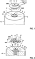
- FIG. 1 shows a perspective view of a connector arrangement 3 in accordance with the invention.
- the connector arrangement 3 is provided for establishing a two-pole electric contact between a battery 42 of an implantable medical device and another component, such as an electronics module of the implantable medical device.
- the implantable medical device may be a pacemaker, an ICD (ICD - implantable cardioverter-defibrillator), a neuro stimulator, e.g. for spinal cord stimulation, a loop recorder, a sensor, such as a pressure sensor, or a leadless pacemaker.
- the connector arrangement 3 comprises a first connector portion 1 and a second connector portion 2.
- the first connector portion 1 includes a first contact element 11 and a pin receptacle 12.
- the first contact element 11 is a metallic element having an annular basic shape (such as a circular ring shape). The shape of the first contact element 11 will be explained in further detail below, e.g. with reference to figures 7 and 8 .
- the pin receptacle 12 is formed as a hole extending through a metallic contact pad 15 of the first connector portion 1.
- the first connector portion 1 is mounted on a printed circuit board (PCB) 41.
- the contact pad 15 comprising the pin receptacle 12 may be mounted in a first side (upper side) 41-1 of the PCB 41, and the first contact element 11 may be mounted on a second side (lower side) 41-2 of the PCB 41, wherein the second side 41-2 of the PCB 41 is opposite to the first site 41-1 of the PCB 41.
- the PCB 41 may form a part of an electronics module of the implantable medical device.
- Figure 1 shows only a portion of a larger PCB 41 of an electronics module of the implantable medical device.
- said portion of the PCB 41 of the electronics module is an extension of the PCB 41 having a circular portion, on which each of the first contact element 11 and the contact pad 15, which forms the pin receptacle 12, are mounted.
- the contact pad 15, which includes the pin receptacle 12, is provided in the form of a surface-mount device (SMD) that is mounted on the first side 41-1 of the PCB 41.
- the first contact element 11 is also a part of an SMD, which is mounted on the second side 41-2 of the PCB 41. This will be explained in further detail below, e.g., with reference to Figures 2-4 .
- the second connector portion 2 comprises a second contact element 21 and a contact pin 22, which are arranged on the battery 42.
- the contact pin 22 axially protrudes from a housing of the battery 42 and has a positive potential (+).
- the contact pin 22 forms a first pole (+) of the battery 42.
- the contact pin 22 may also extend in the interior of the battery 42, as will become apparent, e.g., from the cross-section view in Figure 2 .
- the second contact element 21 is provided in the form of a circular metallic element which extends around the contact pin 22 inside a recess formed in the battery housing.
- the second contact element 21 has a negative potential, thus forming a second pole (-) of the battery 24.
- While the connector arrangement 3 is depicted in a disconnected state in Fig. 1 , it is configured to assume a connected state, in which the first contact element 11 is in contact with the second contact element 21 for connecting the first pole (+), and the contact pin 22 is received in (and in contact with) the pin receptacle 12 for connecting the second pole (-).
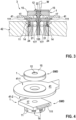
- Figure 2 shows a cross-section view of the connector arrangement 3 of Figure 1 .
- the connector arrangement 3 is still in its disconnected state.
- the first connection element 11 may be mounted on an insulation element 17.
- the insulation element 17 may consist of a plastic material, such as an insulating mold compound.
- the insulation element 17 and the first connection element 11 may together form an SMD, which is mounted on the second side 41-2 of the PCB 41.
- the SMD further comprises bond feet 111, which are electrically connected with the first contact element 11.
- the bond feet 111 may be formed in one (metallic) piece with the first contact elements.
- the cross-section view in Figure 2 further reveals that the PCB 41 has a bore, which is axially aligned with the pin receptacle 12 of the contact pad 15, so as to allow for the contact pin 22 to extend through the bore and into the pin receptacle 12 in the connected state of the connector arrangement 3.
- Figure 2 illustrates several second spring elements 14, which laterally protrude from the ring-shaped first contact element 11.
- the second contact element 21 exhibits a circumferential groove 24.
- the second spring elements 14 form-fittingly and force-fittingly engage with the groove 24 so as to secure a mechanical connection between the first contact element 11 and the second contact element 21.
- the first contact element 11 and the second contact and 21 are configured to be connected with each other by means of a spring connection or snap-in connection in the connected state.
- Figure 3 shows a cross-section view of the connector arrangement 3 of Figures 1 and 2 in its connected state (also referred to as mated condition).
- the contact pin 12 extends through the respective bores provided in the insulation element 17 and the PCB 41 into the pin receptacle 12.
- a contact between the contact pad 15 forming the pin receptacle 12 and the contact pin 22 is established.
- the insulation element 17 and the contact pad 15 comprise inclined insertion surfaces 177, 155, which are configured to guide the contact pin 22 into the bore of the insulation element 17 and the pin receptacle 12. In this way, a potential axial displacement between the insulation element 17, the PCB 41, and/or the contact pad 15 may be compensated to some extent.
- the first contact element 11 engages with the second contact element 21 so as to establish an electrical contact.
- the second spring elements 14 engage with the groove 24 to secure the mechanical connection between the first contact element 11 and the second contact element 12, but also the connection between the first connector portion 1 and the second connector portion 2 as a whole.
- the contact pin 22 may be materially bonded with the pin receptacle 12 in the connected state.
- a metallurgical junction may be provided, e.g., by means of a welded joint, a soldered joint or a brazed joint.
- the material junction may be created by means of a laser welding process W, as schematically indicated in Figure 3 .
- a welding spot or a soldering spot by means of a welding spot or a soldering spot, an extraordinary contact reliability, may be ensured, which is generally required for medical implants.
- the first contact element 11 may be held in contact with the second contact element 21.
- the material bond between the contact pin 22 and the pin receptacle 12 may secure the connection between the first contact element 11 and the second contact element 21.
- the first connector portion 1 is directly connected with the PCB 41 instead of using an additional adapter.
- the number of contact transitions may be reduced to two contact transitions for each pole.
- the first contact element 11 is in contact with the second contact element 21 for connecting the first pole (-)
- the contact pin 22 is be received in the pin receptacle 12 for connecting the second pole (+).
- first contact element 11, the second contact element 21, the contact pin 22, and the pin receptacle 12 may be arranged coaxially.
- each of the first contact element 11, the second contact element 21, the contact pin 22, and the pin receptacle 12 may be arranged coaxially with respect to a common symmetry axis.
- said common symmetry axis may be defined by a main extension axis of the contact pin 22 (pointing in the vertical direction in Fig. 3 ) as well as by a (virtual) axis of the annular basic shape of the first contact element 11 and/or the second contact element 21.
- the connector arrangement 3 may be very volume efficient (i.e. space saving) due to such a coaxial arrangement of its components.
- Figure 4 shows an exploded view of the first connector portion 1 of the connector arrangement 3 in combination with the PCB 41. This view clearly shows the bore that is provided in the PCB 41 for letting pass through the contact pin 12 in the connected state. Further, Figure 4 illustrates an upper side of the insulation element 17 including the bond feet 111.
- Figure 5 shows a cross-section view of the first connector portion 1 of Figure 4 in an assembled state, i. e., in a state, wherein both surface-mount devices (the contact pad 15 as well as the insulation element 17 together with the first contact element 11) are coaxially mounted on a respective side of the PCB 41.
- the assembly of the SMDs may comprise a corresponding reflow soldering steps, in which the SMDs are attached to the PCB 4.
- the cross-section view of Figure 5 also illustrates the inclined insertion surfaces 155, 177 mentioned above.
- Figure 6 shows a perspective view of the first contact element 11 arranged on the insulation element 17.
- the metallic first contact element 11 including the second spring elements 14 may have a plating that comprises, for example, at least one of the following materials: phosphorus-bronze, nickel, and gold.
- the first contact element 11 is provided with an electroless nickel inversion gold (ENIG) plating.
- ENIG electroless nickel inversion gold
- the insulation element 17 may comprise a molded plastic body, which may comprise or consist of one or more liquid-crystal polymers (LCP), for example.
- LCP liquid-crystal polymers
- the first contact element 11 may be partially molded in the insulation element 17.
- Figure 7 shows a perspective view of the first contact element 11 of Figure 6 .
- the first contact element 11 consist of two separate, basically semicircular elements, wherein each of these elements is formed in one piece with a respective bond foot 111.
- Figure 8 shows a perspective view of another exemplary variant of the first (female) contact element 11.
- the first contact element 11, including the second spring elements 14, is formed in one piece, which also includes two solderable bond feet 111.
- the bond feed 111 are provided for soldering the first contact element 11 to the PCB 41.
- a second connector portion 2 is provided on a feedthrough assembly 43 (instead of the battery 42 of Figures 1-3 ).
- feedthrough refers to a component that hermetically seals a conductive pin coming out of the inner assembly of the battery from the exterior (in that case the device electronics).
- the electrically conductive pin transmits electrical energy to the device electronics.
- the second contact element 21 may be plated with gold or another plating material.
- the second contact element 21 is provided inside a recess formed in a housing of the feedthrough assembly 43, similar to what has that been described above with respect to Figures 1 and 2 . As a result, the second contact element 21 does not extend beyond an outer contour of the housing of the feedthrough assembly 42. This is a very volume efficient (i.e., space saving) design.
- Figure 10 shows a cross-section view of the second (male) connector portion 2 of Figure 9 , which is coaxially connected with a part of a first connector portion 1.
- the first connector portion 1 also applies to the first connector portion 1 of the present embodiment.
- the first contact element 11 is force-fittingly and form-fittingly connected with the second contact element 21 by means of a spring connection or snap-in connection, as described above.
- the contact pin 22 extends through bores provided in the insulation element 17 and the PCB 41, respectively.
- the contact pad 15, which forms the pin receptacle 12, is not shown in Figure 10 .
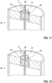
- Figure 11 shows a cross-sectional view of another variant of a second connector portion 2.
- the second contact element 21 is integrated in the housing of the feedthrough assembly 43. Further, the second contact element 21 axially protrudes from a frontend server surface of the housing of the feedthrough assembly 43. In other words, the second conductive 21 defines a portion of an outer contour of the housing of the feedthrough assembly 43.
- Figure 12 shows a cross-section view of yet another variant of second connector portion 2.
- the second connector portion 2 is arranged on a battery 42. Apart from that, the arrangement is very similar to the one described above with reference to Figure 11 .
- the second contact element 21 is integrated in a housing of the battery 42 and axially protrudes from a front surface of said housing.
- Figure 13 shows a perspective view of a PCB 41 and a contact pad 15 forming a pin receptacle 12, wherein the contact pad 15 is not (yet) mounted on the front side 41-1 of the PCB 41.
- the PCB 41 comprises four alignment bores that are arranged around a central bore that is provided so as to let pass through the connection pin 22 of the second connector portion 2 in the connected state of the connector arrangement 3.
- Figure 14 shows the backside 41-2 of the PCB 41 of Figure 13 , as well as an SMD formed by a first contact element 11 that is arranged on an insulation element 17.
- the insulation element 17 comprises four guidance elements 16, which protrude from the four corners of the insulation element 17.
- Figure 15 shows a close-up perspective view of the first contact element 11 and the insulation element 17 including the guidance elements 16.
- Figure 16 shows a cross-section view of the PCB 41, the contact pad 15, and the insulation element 17 of Figures 13-15 in an assembled state.
- each of the insulation element 17 and the contact pad 15 are soldered to a respective side of the PCB 41.
- the guidance elements 16 extend through the alignment bores provided in the PCB 41.
- the guidance elements 16 (in connection with the alignment bores provided in the PCB 41) are configured to axially align the contact element 11, the PCB 41, and the contact pad 15 that forms the pin receptacle 12, e.g., during the reflow soldering processes, which attach the insulation element 17 and the contact pad 15 to the PCB 41.
- the guidance elements 16 are arranged at the insulation element 17 so as to ensure an axial alignment and avoid an unwanted displacement during the reflow process (i.e., while the solder is liquid).
- the guidance elements 16 may laterally engage with a circumferential edge of the contact pad 15 so as to establish said axial alignment, as illustrated in Figure 16 .
- the guidance elements 16 extend through alignment bores provided in the PCB 41.
- a portion of the PCB 41 may be smaller than the insulation element 17 such that the guidance elements 16 may laterally engage with a circumferential edge of said portion of the PCB 41 instead of extending through dedicated alignment bores provided in the PCB 41.
- the contact pad 15 may comprise dedicated alignment bores through which the guidance elements 16 may extend upon assembly of the first connector portion 1.
- Figure 17 shows a cross-section view of the first connector portion 1 of Figure 16 , which is connected to a second connector portion 2 of a battery 42.
- the contact pin 22 may be materially bonded with the pin receptacle 12, e.g., by means of a laser welding process W.
- Figure 18 shows another variant of a PCB 41 and a contact pad 15 forming a pin receptacle 12.
- the contact pad 15 is surrounded by a ring-shaped plastic border 18, wherein the plastic border 18 comprises four alignment bores matching the alignment bores of the PCB 41.
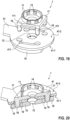
- Figure 19 shows the components already shown in Figure 18 and, in addition, a first contact element 11 that is arranged on an insulation element 17.
- the insulation element 17 has four guidance elements 16, as described above with reference to, e.g., Figures 14-17 .
- bond pads 11 are illustrated, which are configured to establish an electrical connection with the bond feet 111 when the SMD comprising the insulation element 17 and the first contact element 11 is fitted to the second side 41-2 of the PCB 41.
- Figure 20 shows the components of Figure 19 is in an assembled state, wherein the guidance bores and that elements 16 extend into the alignment bores of the plastic border 18.
- the plastic border 18 of the contact pad 15 may be provided with protruding guidance elements, whereas the insulation 17 (instead of the plastic border 18) may have corresponding alignment bores.
- Figure 21 shows a perspective view of the first connector portion 1 of Figure 20 and a battery 42 having a second contact portion 2 as described above in connection with, e.g., Figure 12 .
- the connector assembly 3 is in a disconnected state.
- Figure 22 shows a cross-section view of the connector arrangement 3 of Figure 21 in the connected state, wherein the connector pin is metallurgically bonded with the contact pad 15 that forms the pin receptacle 12.
- the metallurgical bond is created, e.g., by means of a laser welding process W.
- Figure 23 shows a perspective view of a PCB 41 and an array of two contact pads 15, each forming a respective pin receptacle 12.
- the two contact pads 15 are surrounded (and connected to each other) by a common plastic border 18.
- the PCB 41 comprises a total of eight alignment bores.
- eight alignment bores are also provided in the plastic border 18.
- Figure 24 shows the PCB 41 and the contact pad array 15 of Figure 23 as well as two first contact elements 11 that are arranged on respective insulation elements 17.
- Figure 25 shows a cross-section view of the first connector portion 1 of Figure 24 that is connected to a second connector portion 2 of a battery 42.
- each contact pin 22 may be welded to the respective contact pad 15 in the mated condition of the connector arrangement 3.
- corresponding welding spots may be created by means of a laser welding process W.
- Figure 26 shows a perspective view of yet a further variant of a connector arrangement 3 in the connected state.
- the contact pad 15 is arranged directly on the PCB 41 and has a ring-shaped solderable surface that surrounds the pin receptacle 12.
- a distal end of the contact pin 22 extends through the pin receptacle 12 and axially protrudes above the PCB 41 and the solderable surface of the contact pad 15.
- the contact pin 22 may be plated, e.g., with gold, palladium or ENIG, so as to enable soldering.
- Figure 27 shows the connector arrangement of Figure 26 , wherein the contact pin 22 is soldered to the pin receptacle 12 (see the soft solder 31).
- the material bond between the connector pin 22 and the pin receptacle 12 is created by means of a soft solder process.
- Figure 28 shows a cross-section view of the connector arrangement 3 of Figure 27 .
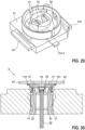
- Figure 29 shows another variant of a first connector portion 1, wherein the pin receptacle 12 is formed by a first spring element 13.
- the first spring element 13 is configured to clamp the distal end of the contact pin 22 in the connected state, thereby establishing a form-fitting and force fitting connection between the pin receptacle 12 and the contact pin 22.
- the first spring element 13 is connected with one or more solderable bond feet 111-1.
- the first spring element 13 and the bond feet 111-1 that are illustrated in Figure 29 may also be formed in one piece.
- the material and/or plating of the first spring element 13 and/or of the bond feet 111-1 may be the same as the material and/or of the first contact element 11 (which may have, e.g., a plating comprising phosphorous, bronze, nickel, gold or ENIG, as explained above).
- Figure 30 shows a cross-section view of the first connector portion 1 of Figure 29 that is connected with a second connector portion 2.
- the contact pin 22 is clamped inside the first spring element 13. It should be noted that here, the contact pin 22 does not extend through the PCB 41 in the connected state.
- the first contact element 11 and the second contact element 21 are connected by means of a spring connection or snap-in connection, as described above.
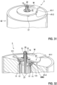
- Figure 31 shows yet another variant of a connector assembly 3 having a first spring connection 13 for securing the contact pin 22 in the connected position.
- the first spring connection 13 is arranged on the contact pad 15, i.e., on the first side 41-1 of the PCB 41.
- the distal end of the contact pin 22 extends through the PCB and is clamped by the first spring element 13.
- a metallurgical bond may be created between the first spring element 13 and the contact pin 22, e. g., by means of a laser welding process W.
- Figure 32 shows a cross-section view of the connector assembly 3 of Figure 31 .
Claims (15)
- Dispositif médical implantable possédant un agencement de connecteurs (3) permettant d'établir un contact électrique bipolaire entre des composants du dispositif médical implantable (4), l'agencement de connecteurs (3) comprenantun premier segment de connecteur (1) comprenant un premier élément de contact (11) et un réceptacle à broche (12) ; etun deuxième segment de connecteur (2) comprenant un deuxième élément de contact (21) et une broche de contact (22) ; etune carte de circuit imprimé (41)dans lequel l'agencement de connecteurs (3) est conçu pour assurer un état connecté, par lequel
le premier élément de contact (11) est en contact avec le deuxième élément de contact (21) ; et
la broche de contact (22) est réceptionnée dans le réceptacle à broche (12) ;
dans lequel au moins une partie du premier segment de connecteur (1), ou au moins une partie du deuxième segment de connecteur (2), est montée sur la carte de circuit imprimé (41). - Dispositif médical implantable selon la revendication 1, dans lequel le premier segment de connecteur (1), ou le deuxième segment de connecteur (2), forme au moins une partie d'un dispositif de montage en surface (SMD) qui est monté sur la carte de circuit imprimé (41).
- Dispositif médical implantable selon l'une des revendications précédentes, dans lequel le réceptacle à broche (12) est monté sur un premier côté (41-1) de la carte de circuit imprimé (41) et le premier élément de contact (11) est monté sur un deuxième côté (41-2) de la carte de circuit imprimé (41) qui est opposé au premier côté (41-1).
- Dispositif médical implantable selon l'une des revendications précédentes, dans lequel l'agencement de connecteurs (3) est dans l'état connecté et la broche de contact (22) est liée matériellement avec le réceptacle à broche (12).
- Dispositif médical implantable selon la revendication 4, dans lequel la broche de contact (22) est reliée avec le réceptacle à broche (12) au moyen d'au moins un élément parmi : un j oint amalgamé, un j oint soudé et un joint brasé.
- Dispositif médical implantable selon l'une des revendications précédentes, dans lequel l'agencement de connecteurs (3) est dans l'état connecté et la broche de contact (22) est connectée par complémentarité des formes et/ou par complémentarité des forces au réceptacle à broche (12).
- Dispositif médical implantable selon l'une des revendications précédentes, dans lequel le premier segment de connecteur (1) comprend un premier élément de ressort (13) qui est conçu pour établir une connexion par complémentarité des formes et/ou par complémentarité des forces entre le réceptacle à broche (12) et la broche de contact (22) dans l'état connecté de l'agencement de connecteurs (3).
- Dispositif médical implantable selon l'une des revendications précédentes, dans lequel le premier élément de contact (11) et le deuxième élément de contact (21) sont conçus pour être connectés l'un avec l'autre au moyen d'une connexion par ressort, et/ou au moyen d'une connexion encliquetable, dans l'état connecté de l'agencement de connecteurs (3).
- Dispositif médical implantable selon la revendication 8, dans lequel l'un parmi le premier élément de contact (11) et le deuxième élément de contact (21) comprend au moins un deuxième élément de ressort (14) et l'autre parmi le premier élément de contact (11) et le deuxième élément de contact (21) comprend au moins une rainure (24), dans lequel l'au moins un deuxième élément de ressort (14) se met en prise avec l'au moins une rainure (24) dans l'état connecté de l'agencement de connecteurs (3).
- Dispositif médical implantable selon l'une des revendications précédentes, dans lequel le premier élément de contact (11) et/ou le deuxième élément de contact (21) ont une forme basique annulaire.
- Dispositif médical implantable selon l'une des revendications précédentes, dans lequel chacun parmi le premier élément de contact (11), le deuxième élément de contact (21), la broche de contact (22) et le réceptacle à broche (12) sont agencés co-axialement par rapport à un axe de symétrie commun dans l'état connecté de l'agencement de connecteurs (3).
- Dispositif médical implantable selon l'une des revendications précédentes, dans lequel le premier segment de connecteur (1) comprend un plot de contact (15).
- Dispositif médical implantable selon la revendication 12, dans lequel le premier segment de connecteur (1) comprend au moins un élément de guidage (16) conçu pour aligner le premier élément de contact (11) et le plot de contact (15).
- Dispositif médical implantable selon l'une des revendications 2 à 13, dans lequel le dispositif de montage en surface (SMD) est monté sur une carte de circuit imprimé (41) qui est une partie d'un module électronique du dispositif médical implantable (4).
- Dispositif médical implantable selon la revendication 14, dans lequel le premier segment de connecteur (1) est monté sur la carte de circuit imprimé (41) et le deuxième segment de connecteur (2) est agencé sur une pile (42) ou sur un condensateur du dispositif médical implantable (4).
Priority Applications (3)
| Application Number | Priority Date | Filing Date | Title |
|---|---|---|---|
| JP2019233614A JP2020121110A (ja) | 2019-01-30 | 2019-12-25 | 植込型医療デバイスの構成要素間に2極の電気接触を確立するコネクタ装置、及びかかるコネクタ装置を有する植込型医療デバイス |
| US16/775,498 US11229797B2 (en) | 2019-01-30 | 2020-01-29 | Two-pole electric contact connector for implantable medical device components |
| US17/577,075 US20220134115A1 (en) | 2019-01-30 | 2022-01-17 | Two-pole electric contact connector for implantable medical device components |
Applications Claiming Priority (1)
| Application Number | Priority Date | Filing Date | Title |
|---|---|---|---|
| EP19154499 | 2019-01-30 |
Publications (2)
| Publication Number | Publication Date |
|---|---|
| EP3689417A1 EP3689417A1 (fr) | 2020-08-05 |
| EP3689417B1 true EP3689417B1 (fr) | 2023-06-07 |
Family
ID=67437058
Family Applications (1)
| Application Number | Title | Priority Date | Filing Date |
|---|---|---|---|
| EP19192352.3A Active EP3689417B1 (fr) | 2019-01-30 | 2019-08-19 | Dispositif médical implantable avec un agencement de connecteur pour établir un contact électrique bipolaire entre des composants |
Country Status (3)
| Country | Link |
|---|---|
| US (2) | US11229797B2 (fr) |
| EP (1) | EP3689417B1 (fr) |
| JP (1) | JP2020121110A (fr) |
Families Citing this family (1)
| Publication number | Priority date | Publication date | Assignee | Title |
|---|---|---|---|---|
| JP7413198B2 (ja) * | 2020-08-07 | 2024-01-15 | 株式会社三共 | 遊技機 |
Family Cites Families (12)
| Publication number | Priority date | Publication date | Assignee | Title |
|---|---|---|---|---|
| JPS62285378A (ja) * | 1986-06-04 | 1987-12-11 | ヒロセ電機株式会社 | 雌形同軸コネクタとその製造方法 |
| US4827378A (en) * | 1988-06-15 | 1989-05-02 | Rockwell International Corporation | Jack coaxial connector EMI shielding apparatus |
| US5103818A (en) * | 1990-11-13 | 1992-04-14 | Siemens-Pacesetter, Inc. | System and method for completing electrical connections in an implantable medical device |
| US5791911A (en) * | 1996-10-25 | 1998-08-11 | International Business Machines Corporation | Coaxial interconnect devices and methods of making the same |
| US6079986A (en) * | 1998-02-07 | 2000-06-27 | Berg Technology, Inc. | Stacking coaxial connector for three printed circuit boards |
| JP2002298940A (ja) * | 2001-03-30 | 2002-10-11 | Jst Mfg Co Ltd | 樹脂ハンダを用いた電気接触子、電気コネクタ及びこれらのプリント配線板への接続方法 |
| JP4076157B2 (ja) * | 2003-07-30 | 2008-04-16 | ヒロセ電機株式会社 | 同軸電気コネクタ |
| JP2006066384A (ja) * | 2004-07-27 | 2006-03-09 | Hosiden Corp | 基板対基板接続用同軸コネクタ |
| US20070150020A1 (en) | 2005-12-28 | 2007-06-28 | Hokanson Karl E | Externally oriented battery feedthrough with integral connector |
| CN201498718U (zh) * | 2009-07-24 | 2010-06-02 | 富士康(昆山)电脑接插件有限公司 | 电连接器 |
| US9136639B2 (en) * | 2012-06-01 | 2015-09-15 | Hamilton Sundstrand Corporation | Electrical connector receptacle for mounting within an explosion proof enclosure and method of mounting |
| US10003063B2 (en) | 2015-04-22 | 2018-06-19 | Medtronic, Inc. | Battery assembly for implantable medical device |
-
2019
- 2019-08-19 EP EP19192352.3A patent/EP3689417B1/fr active Active
- 2019-12-25 JP JP2019233614A patent/JP2020121110A/ja active Pending
-
2020
- 2020-01-29 US US16/775,498 patent/US11229797B2/en active Active
-
2022
- 2022-01-17 US US17/577,075 patent/US20220134115A1/en active Pending
Also Published As
| Publication number | Publication date |
|---|---|
| US11229797B2 (en) | 2022-01-25 |
| US20200238092A1 (en) | 2020-07-30 |
| US20220134115A1 (en) | 2022-05-05 |
| JP2020121110A (ja) | 2020-08-13 |
| EP3689417A1 (fr) | 2020-08-05 |
Similar Documents
| Publication | Publication Date | Title |
|---|---|---|
| US6963780B2 (en) | Implantable medical device including a surface-mount terminal array | |
| US5103818A (en) | System and method for completing electrical connections in an implantable medical device | |
| US8700159B2 (en) | Methods of manufacturing an implantable pulse generator | |
| EP1928547B1 (fr) | Dispositif médical implantable avec boîtier et connecteur soudables | |
| US8593816B2 (en) | Compact connector assembly for implantable medical device | |
| US20130127567A1 (en) | Capacitive filtered feedthrough array for implantable medical device | |
| US5877472A (en) | System for laser-welding components of an implantable device | |
| US11588213B2 (en) | Battery connectors for implantable medical devices | |
| JP3956920B2 (ja) | コネクタ | |
| CN110034430B (zh) | 电连接器及其组装方法 | |
| EP2954929A1 (fr) | Ensemble connecteur de conducteur, dispositif médical et son procédé de fabrication | |
| EP2968953B1 (fr) | Dispositif médical implantable et son ensemble | |
| US20220134115A1 (en) | Two-pole electric contact connector for implantable medical device components | |
| US6626680B2 (en) | Wire bonding surface | |
| EP3069753A1 (fr) | Dispositif médical implantable et son procédé de fabrication | |
| KR101238416B1 (ko) | Led모듈 | |
| KR20030041796A (ko) | 핀-그리드-어레이 전기 커넥터 | |
| EP1501599A1 (fr) | Dispositif connecte a des stimulateurs cardiaques | |
| US20230096287A1 (en) | Feedthrough with integrated electrode and medical device | |
| EP3332452B1 (fr) | Contact monté en surface, ensemble dispositif électronique | |
| CN217848536U (zh) | 一种用于插座或插头的高可靠性滤波电连接器 | |
| CN217387599U (zh) | 一种Type-C母端电连接器 | |
| CN114628931A (zh) | 一种Type-C母端电连接器 | |
| JP2000223828A (ja) | 電気部品の通電部構造 |
Legal Events
| Date | Code | Title | Description |
|---|---|---|---|
| PUAI | Public reference made under article 153(3) epc to a published international application that has entered the european phase |
Free format text: ORIGINAL CODE: 0009012 |
|
| STAA | Information on the status of an ep patent application or granted ep patent |
Free format text: STATUS: THE APPLICATION HAS BEEN PUBLISHED |
|
| AK | Designated contracting states |
Kind code of ref document: A1 Designated state(s): AL AT BE BG CH CY CZ DE DK EE ES FI FR GB GR HR HU IE IS IT LI LT LU LV MC MK MT NL NO PL PT RO RS SE SI SK SM TR |
|
| AX | Request for extension of the european patent |
Extension state: BA ME |
|
| STAA | Information on the status of an ep patent application or granted ep patent |
Free format text: STATUS: REQUEST FOR EXAMINATION WAS MADE |
|
| 17P | Request for examination filed |
Effective date: 20210203 |
|
| RBV | Designated contracting states (corrected) |
Designated state(s): AL AT BE BG CH CY CZ DE DK EE ES FI FR GB GR HR HU IE IS IT LI LT LU LV MC MK MT NL NO PL PT RO RS SE SI SK SM TR |
|
| GRAP | Despatch of communication of intention to grant a patent |
Free format text: ORIGINAL CODE: EPIDOSNIGR1 |
|
| STAA | Information on the status of an ep patent application or granted ep patent |
Free format text: STATUS: GRANT OF PATENT IS INTENDED |
|
| RIC1 | Information provided on ipc code assigned before grant |
Ipc: H01R 103/00 20060101ALN20221116BHEP Ipc: H01R 13/11 20060101ALN20221116BHEP Ipc: H01R 24/38 20110101ALN20221116BHEP Ipc: H01R 13/627 20060101ALN20221116BHEP Ipc: H01R 12/57 20110101ALN20221116BHEP Ipc: H01M 50/519 20210101ALI20221116BHEP Ipc: H01M 50/503 20210101ALI20221116BHEP Ipc: A61N 1/375 20060101ALI20221116BHEP Ipc: H01R 24/50 20110101AFI20221116BHEP |
|
| INTG | Intention to grant announced |
Effective date: 20221206 |
|
| REG | Reference to a national code |
Ref country code: DE Ref legal event code: R079 Ref document number: 602019029845 Country of ref document: DE Free format text: PREVIOUS MAIN CLASS: A61N0001375000 Ipc: H01R0024500000 Ref country code: DE Ref legal event code: R079 Free format text: PREVIOUS MAIN CLASS: A61N0001375000 Ipc: H01R0024500000 |
|
| GRAJ | Information related to disapproval of communication of intention to grant by the applicant or resumption of examination proceedings by the epo deleted |
Free format text: ORIGINAL CODE: EPIDOSDIGR1 |
|
| STAA | Information on the status of an ep patent application or granted ep patent |
Free format text: STATUS: REQUEST FOR EXAMINATION WAS MADE |
|
| GRAP | Despatch of communication of intention to grant a patent |
Free format text: ORIGINAL CODE: EPIDOSNIGR1 |
|
| STAA | Information on the status of an ep patent application or granted ep patent |
Free format text: STATUS: GRANT OF PATENT IS INTENDED |
|
| GRAS | Grant fee paid |
Free format text: ORIGINAL CODE: EPIDOSNIGR3 |
|
| GRAA | (expected) grant |
Free format text: ORIGINAL CODE: 0009210 |
|
| STAA | Information on the status of an ep patent application or granted ep patent |
Free format text: STATUS: THE PATENT HAS BEEN GRANTED |
|
| INTC | Intention to grant announced (deleted) | ||
| RIC1 | Information provided on ipc code assigned before grant |
Ipc: H01R 103/00 20060101ALN20230331BHEP Ipc: H01R 13/11 20060101ALN20230331BHEP Ipc: H01R 24/38 20110101ALN20230331BHEP Ipc: H01R 13/627 20060101ALN20230331BHEP Ipc: H01R 12/57 20110101ALN20230331BHEP Ipc: H01M 50/519 20210101ALI20230331BHEP Ipc: H01M 50/503 20210101ALI20230331BHEP Ipc: A61N 1/375 20060101ALI20230331BHEP Ipc: H01R 24/50 20110101AFI20230331BHEP |
|
| INTG | Intention to grant announced |
Effective date: 20230428 |
|
| AK | Designated contracting states |
Kind code of ref document: B1 Designated state(s): AL AT BE BG CH CY CZ DE DK EE ES FI FR GB GR HR HU IE IS IT LI LT LU LV MC MK MT NL NO PL PT RO RS SE SI SK SM TR |
|
| REG | Reference to a national code |
Ref country code: GB Ref legal event code: FG4D |
|
| REG | Reference to a national code |
Ref country code: CH Ref legal event code: EP Ref country code: AT Ref legal event code: REF Ref document number: 1577733 Country of ref document: AT Kind code of ref document: T Effective date: 20230615 Ref country code: DE Ref legal event code: R096 Ref document number: 602019029845 Country of ref document: DE |
|
| P01 | Opt-out of the competence of the unified patent court (upc) registered |
Effective date: 20230612 |
|
| REG | Reference to a national code |
Ref country code: LT Ref legal event code: MG9D |
|
| REG | Reference to a national code |
Ref country code: NL Ref legal event code: MP Effective date: 20230607 |
|
| PG25 | Lapsed in a contracting state [announced via postgrant information from national office to epo] |
Ref country code: SE Free format text: LAPSE BECAUSE OF FAILURE TO SUBMIT A TRANSLATION OF THE DESCRIPTION OR TO PAY THE FEE WITHIN THE PRESCRIBED TIME-LIMIT Effective date: 20230607 Ref country code: NO Free format text: LAPSE BECAUSE OF FAILURE TO SUBMIT A TRANSLATION OF THE DESCRIPTION OR TO PAY THE FEE WITHIN THE PRESCRIBED TIME-LIMIT Effective date: 20230907 Ref country code: ES Free format text: LAPSE BECAUSE OF FAILURE TO SUBMIT A TRANSLATION OF THE DESCRIPTION OR TO PAY THE FEE WITHIN THE PRESCRIBED TIME-LIMIT Effective date: 20230607 |
|
| PGFP | Annual fee paid to national office [announced via postgrant information from national office to epo] |
Ref country code: IE Payment date: 20230821 Year of fee payment: 5 Ref country code: CH Payment date: 20230902 Year of fee payment: 5 |
|
| REG | Reference to a national code |
Ref country code: AT Ref legal event code: MK05 Ref document number: 1577733 Country of ref document: AT Kind code of ref document: T Effective date: 20230607 |
|
| PG25 | Lapsed in a contracting state [announced via postgrant information from national office to epo] |
Ref country code: RS Free format text: LAPSE BECAUSE OF FAILURE TO SUBMIT A TRANSLATION OF THE DESCRIPTION OR TO PAY THE FEE WITHIN THE PRESCRIBED TIME-LIMIT Effective date: 20230607 Ref country code: NL Free format text: LAPSE BECAUSE OF FAILURE TO SUBMIT A TRANSLATION OF THE DESCRIPTION OR TO PAY THE FEE WITHIN THE PRESCRIBED TIME-LIMIT Effective date: 20230607 Ref country code: LV Free format text: LAPSE BECAUSE OF FAILURE TO SUBMIT A TRANSLATION OF THE DESCRIPTION OR TO PAY THE FEE WITHIN THE PRESCRIBED TIME-LIMIT Effective date: 20230607 Ref country code: LT Free format text: LAPSE BECAUSE OF FAILURE TO SUBMIT A TRANSLATION OF THE DESCRIPTION OR TO PAY THE FEE WITHIN THE PRESCRIBED TIME-LIMIT Effective date: 20230607 Ref country code: HR Free format text: LAPSE BECAUSE OF FAILURE TO SUBMIT A TRANSLATION OF THE DESCRIPTION OR TO PAY THE FEE WITHIN THE PRESCRIBED TIME-LIMIT Effective date: 20230607 Ref country code: GR Free format text: LAPSE BECAUSE OF FAILURE TO SUBMIT A TRANSLATION OF THE DESCRIPTION OR TO PAY THE FEE WITHIN THE PRESCRIBED TIME-LIMIT Effective date: 20230908 |
|
| PGFP | Annual fee paid to national office [announced via postgrant information from national office to epo] |
Ref country code: DE Payment date: 20230822 Year of fee payment: 5 |
|
| PG25 | Lapsed in a contracting state [announced via postgrant information from national office to epo] |
Ref country code: FI Free format text: LAPSE BECAUSE OF FAILURE TO SUBMIT A TRANSLATION OF THE DESCRIPTION OR TO PAY THE FEE WITHIN THE PRESCRIBED TIME-LIMIT Effective date: 20230607 |
|
| PG25 | Lapsed in a contracting state [announced via postgrant information from national office to epo] |
Ref country code: SK Free format text: LAPSE BECAUSE OF FAILURE TO SUBMIT A TRANSLATION OF THE DESCRIPTION OR TO PAY THE FEE WITHIN THE PRESCRIBED TIME-LIMIT Effective date: 20230607 |
|
| PG25 | Lapsed in a contracting state [announced via postgrant information from national office to epo] |
Ref country code: IS Free format text: LAPSE BECAUSE OF FAILURE TO SUBMIT A TRANSLATION OF THE DESCRIPTION OR TO PAY THE FEE WITHIN THE PRESCRIBED TIME-LIMIT Effective date: 20231007 |
|
| PG25 | Lapsed in a contracting state [announced via postgrant information from national office to epo] |
Ref country code: SM Free format text: LAPSE BECAUSE OF FAILURE TO SUBMIT A TRANSLATION OF THE DESCRIPTION OR TO PAY THE FEE WITHIN THE PRESCRIBED TIME-LIMIT Effective date: 20230607 Ref country code: SK Free format text: LAPSE BECAUSE OF FAILURE TO SUBMIT A TRANSLATION OF THE DESCRIPTION OR TO PAY THE FEE WITHIN THE PRESCRIBED TIME-LIMIT Effective date: 20230607 Ref country code: RO Free format text: LAPSE BECAUSE OF FAILURE TO SUBMIT A TRANSLATION OF THE DESCRIPTION OR TO PAY THE FEE WITHIN THE PRESCRIBED TIME-LIMIT Effective date: 20230607 Ref country code: PT Free format text: LAPSE BECAUSE OF FAILURE TO SUBMIT A TRANSLATION OF THE DESCRIPTION OR TO PAY THE FEE WITHIN THE PRESCRIBED TIME-LIMIT Effective date: 20231009 Ref country code: IS Free format text: LAPSE BECAUSE OF FAILURE TO SUBMIT A TRANSLATION OF THE DESCRIPTION OR TO PAY THE FEE WITHIN THE PRESCRIBED TIME-LIMIT Effective date: 20231007 Ref country code: EE Free format text: LAPSE BECAUSE OF FAILURE TO SUBMIT A TRANSLATION OF THE DESCRIPTION OR TO PAY THE FEE WITHIN THE PRESCRIBED TIME-LIMIT Effective date: 20230607 Ref country code: CZ Free format text: LAPSE BECAUSE OF FAILURE TO SUBMIT A TRANSLATION OF THE DESCRIPTION OR TO PAY THE FEE WITHIN THE PRESCRIBED TIME-LIMIT Effective date: 20230607 Ref country code: AT Free format text: LAPSE BECAUSE OF FAILURE TO SUBMIT A TRANSLATION OF THE DESCRIPTION OR TO PAY THE FEE WITHIN THE PRESCRIBED TIME-LIMIT Effective date: 20230607 |
|
| PG25 | Lapsed in a contracting state [announced via postgrant information from national office to epo] |
Ref country code: PL Free format text: LAPSE BECAUSE OF FAILURE TO SUBMIT A TRANSLATION OF THE DESCRIPTION OR TO PAY THE FEE WITHIN THE PRESCRIBED TIME-LIMIT Effective date: 20230607 |
|
| REG | Reference to a national code |
Ref country code: DE Ref legal event code: R097 Ref document number: 602019029845 Country of ref document: DE |
|
| PG25 | Lapsed in a contracting state [announced via postgrant information from national office to epo] |
Ref country code: MC Free format text: LAPSE BECAUSE OF FAILURE TO SUBMIT A TRANSLATION OF THE DESCRIPTION OR TO PAY THE FEE WITHIN THE PRESCRIBED TIME-LIMIT Effective date: 20230607 |
|
| PG25 | Lapsed in a contracting state [announced via postgrant information from national office to epo] |
Ref country code: MC Free format text: LAPSE BECAUSE OF FAILURE TO SUBMIT A TRANSLATION OF THE DESCRIPTION OR TO PAY THE FEE WITHIN THE PRESCRIBED TIME-LIMIT Effective date: 20230607 |
|
| PLBE | No opposition filed within time limit |
Free format text: ORIGINAL CODE: 0009261 |
|
| STAA | Information on the status of an ep patent application or granted ep patent |
Free format text: STATUS: NO OPPOSITION FILED WITHIN TIME LIMIT |
|
| PG25 | Lapsed in a contracting state [announced via postgrant information from national office to epo] |
Ref country code: LU Free format text: LAPSE BECAUSE OF NON-PAYMENT OF DUE FEES Effective date: 20230819 |