EP3687153B1 - Camera module and assembly process therefor - Google Patents
Camera module and assembly process therefor Download PDFInfo
- Publication number
- EP3687153B1 EP3687153B1 EP18932972.5A EP18932972A EP3687153B1 EP 3687153 B1 EP3687153 B1 EP 3687153B1 EP 18932972 A EP18932972 A EP 18932972A EP 3687153 B1 EP3687153 B1 EP 3687153B1
- Authority
- EP
- European Patent Office
- Prior art keywords
- connector
- lens
- circuit board
- camera module
- present disclosure
- Prior art date
- Legal status (The legal status is an assumption and is not a legal conclusion. Google has not performed a legal analysis and makes no representation as to the accuracy of the status listed.)
- Active
Links
Images

Classifications
-
- H—ELECTRICITY
- H04—ELECTRIC COMMUNICATION TECHNIQUE
- H04N—PICTORIAL COMMUNICATION, e.g. TELEVISION
- H04N23/00—Cameras or camera modules comprising electronic image sensors; Control thereof
- H04N23/50—Constructional details
-
- H—ELECTRICITY
- H04—ELECTRIC COMMUNICATION TECHNIQUE
- H04N—PICTORIAL COMMUNICATION, e.g. TELEVISION
- H04N23/00—Cameras or camera modules comprising electronic image sensors; Control thereof
-
- H—ELECTRICITY
- H04—ELECTRIC COMMUNICATION TECHNIQUE
- H04N—PICTORIAL COMMUNICATION, e.g. TELEVISION
- H04N23/00—Cameras or camera modules comprising electronic image sensors; Control thereof
- H04N23/50—Constructional details
- H04N23/54—Mounting of pick-up tubes, electronic image sensors, deviation or focusing coils
-
- H—ELECTRICITY
- H04—ELECTRIC COMMUNICATION TECHNIQUE
- H04N—PICTORIAL COMMUNICATION, e.g. TELEVISION
- H04N23/00—Cameras or camera modules comprising electronic image sensors; Control thereof
- H04N23/50—Constructional details
- H04N23/55—Optical parts specially adapted for electronic image sensors; Mounting thereof
Definitions
- the present disclosure relates to a camera module having a connection between an optical lens and a circuit board, and an assembly process of the camera module.
- a lens and a circuit board are assembled mainly in the following kinds of ways: 1: the lens and a lens holder are fixed to the circuit board (circuit board assembly) by glue; 2: for a non-threaded split type lens, a lens flange and the lens holder are generally fixed by glue, and the lens holder is then fixed to the circuit board by thread or glue; and 3: for a threaded lens, the lens and the lens holder are generally fixed after the thread is filled with glue, and the lens holder and the circuit board are locked by thread or fixed by glue.
- glue to fix the circuit board to the lens has the following defects:
- Document US 2018/084161 A1 discloses a camera including a lens part in which a lens is installed, a housing coupled to the lens part, and a substrate electrically coupled to the lens part., wherein the housing includes a metal compound.
- a heating-element groove is formed over one or more surfaces of the housing.
- a heating element is disposed in the heating-element groove.
- the substrate includes a coupling part coupled with the heating element.
- An object of the present disclosure is to provide a camera module and an assembly process that are capable of improving imaging quality.
- the present disclosure provides a camera module according to claim 1, and an assembly process of the camera module according to claim 8.
- a connector mounting hole is disposed in the lens, and the connector is mounted in the connector mounting hole.
- the body portion and the connection pins are of an integrally formed configuration.
- connection pins are detachably connected to the body portion.
- a material of the connector is carbon steel.
- the circuit board is provided with an image sensor and electronic components.
- the lens is an integrated lens.
- the present disclosure also provides an assembly process of the camera module as described above, which includes: a. mounting connection pins to the body portion to form a connector and then connecting the connector with the lens, or directly connecting a connector with the lens; b. focus-adjusting the lens and the image sensor on the circuit board; and c. fixing the connector to the circuit board by welding using a solder.
- connection pins and the circuit board need to be plated.
- the connector is provided between the lens and the circuit board, so that the camera module of the present disclosure can be more conveniently assembled.
- the connection between the lens and the circuit board is achieved by welding the connector to the circuit board, which effectively avoids the defects caused by the connection between the lens and the circuit board implemented by glue in the related art, and is advantageous for ensuring an imaging quality of the camera module.
- the circuit board includes a thin plate and a steel sheet reinforced plate.
- a structural strength of the circuit board can be enhanced; and on the other hand, the steel sheet reinforced plate has the advantage of rapid heat dissipation, which can quickly take away the heat generated when a photosensitive chip works and ensure the uniform heat of the overall circuit board so that a deformation amount of the circuit board can be effectively controlled, thereby greatly improving the imaging quality of the camera module in a working state.
- a thermal coefficient of the steel sheet reinforced plate is greater than a thermal coefficient of the connector.
- the connector is made of carbon steel.
- orientations or positional relationships described by the terms “longitudinal”, “transverse”, “upper”, “lower”, “front”, “rear”, “left”, “right”, “vertical”, “horizontal”, “top”, “bottom”, “inner” and “outer” are based on the orientations or positional relationships shown in the related drawings. These terms are merely used for the sake of facilitating describing the present disclosure and simplifying the description, and do not indicate or imply that the device or element as referred to must have a particular orientation, or must be constructed or operated in a particular orientation. Therefore, the above terms should not be construed as limiting the scope of the present disclosure.
- the camera module of the present disclosure includes a lens 1, a circuit board 2, and a connector 3.
- the lens 1 includes a lens barrel portion and a flange portion, and the flange portion is located on a lower side of the lens barrel portion and is connected to the lens barrel portion.
- the lens barrel portion of the lens 1 is made of a metal material; for example, a material such as copper or aluminum may be used. This design solves the problem of poor consistency of the heat compensation amount caused by different thermal expansion coefficients when the split lens holder and lens are connected by thread and glue or by thread alone.
- the flange portion of the lens 1 is connected to the connector 3.
- the connector 3 is disposed between the lens 1 and the circuit board 2.
- a connector mounting hole is disposed in the lens 1, the connector 3 is mounted in the connector mounting hole, and the other end of the connector 3 is welded to the circuit board 2.
- the connector 3 includes a body portion 31 and connection pins 32.
- the connection pins 32 are disposed on a side of the body portion 31 near the circuit board 2.
- the body portion 31 is detachably connected to the lens 1, and the connection pins 32 and the circuit board 2 are fixed by welding.
- the connector 3 is disposed between the lens 1 and the circuit board 2 so that the camera module of the present disclosure can be assembled more conveniently.
- the connection between the lens 1 and the circuit board 2 is achieved by welding the connector 3 and the circuit board 2, which effectively avoids the defects caused by the connection between the lens and the circuit board implemented by glue in the related art, which is advantageous for ensuring the imaging quality of the camera module.
- the circuit board 2 of the present disclosure includes a thin plate 21 and a steel sheet reinforced plate 22.
- the thin plate 21 is located on an upper side
- the steel sheet reinforced plate 22 is located on a lower side of the thin plate 21 and fitted and fixed to the thin plate 21.
- the thin plate 21 of the circuit board 2 is provided with an image sensor, a photosensitive chip 23, electronic components 24, and a flexible connection strip 25.
- the circuit board 2 of the present disclosure is further provided with pads 2a for carrying welding spots.
- the connector 3 and the circuit board 2 of the present disclosure are fixedly connected by welding. Specifically, the connection pins 32 are welded and fixed to the pads 2a on the circuit board 2 through a solder 4.
- the pads 2a may be directly disposed on the thin plate 21.
- through holes may be provided in the thin plate 21 of the circuit board 2, and the pads 2a are disposed in the through holes and fixed with the steel sheet reinforced plate 22. That is, the pads 2a may be disposed on the steel sheet reinforced plate 22.
- the circuit board 2 of the present disclosure includes a thin plate 21 and a steel sheet reinforced plate 22.
- a structural strength of the circuit board 2 can be enhanced; and on the other hand, the steel sheet reinforced plate 22 has the advantage of rapid heat dissipation, which can quickly take away the heat generated when the photosensitive chip 23 works and ensure the uniform heat of the overall circuit board 2 so that a deformation amount of the circuit board 2 can be effectively controlled, thereby greatly improving the imaging quality of the camera module in a working state.
- a thermal coefficient of the steel sheet reinforced plate 22 is greater than a thermal coefficient of the connection pins 32.
- the connector 3 is made of carbon steel.
- the connector 3 is of an integrally formed configuration, that is, the body portion 31 and the connection pins 32 of the connector 3 are integrally formed.
- the connector 3 of the present disclosure may be manufactured by die-casting.
- the body portion 31 and the connection pins 32 of the connector 3 are detachably connected, that is, the connection pins 32, as a separate assembly, need to be assembled to the body portion 31 first.
- threaded holes are provided in the body portion 31, and the connection pins 32 are mounted in the threaded holes of the body portion 31.
- the present disclosure also provides an assembly process of the camera module, which includes: a. mounting connection pins to the body portion to form a connector and then connecting the connector with the lens, or directly connecting a connector with the lens; b. focus-adjusting the lens 1 and the image sensor on the circuit board 2; and c. fixing the connector 3 to the circuit board 2 by welding using the solder 4.
- the lens 1, the connector 3 and the circuit board 2 that have passed the inspection are selected. If the selected connector 3 is a separate assembly, the connector 3 is connected to the flange portion of the lens 1. If the selected connector 3 is not a separate assembly, the connection pins 32 are mounted to the body portion 31 of the connector 3 (if an integrally formed connector 3 is used, it is not necessary to separately mount the connection pins 32). After that, an automatic spot-soldering machine applies the solder 4 (which may be solder paste, solder ball, solder wire, etc.) at the pads 2a of the circuit board 2.
- solder 4 which may be solder paste, solder ball, solder wire, etc.
- a relative position of the lens 1 to the circuit board 2 is adjusted, the lens 1 and the image sensor on the circuit board 2 are focus-adjusted, and the optical center, optical axis, and resolution are adjusted.
- the welding machine equipment is automatically turned on, and the solder 4 at the pads 2a is heated and melted to achieve fixing.
- the optical performance of the camera is tested.
- a test completion status is shown on an LED display, and the assembling of the lens 1 and the circuit board 2 is completed. Then, other components may be assembled.
- the lens 1, the connector 3 and the circuit board 2 that have passed the inspection are selected. If the selected connector 3 is a separate assembly, the connector 3 is connected to the flange portion of the lens 1. If the selected connector 3 is not a separate assembly, the connection pins 32 are mounted to the body portion 31 of the connector 3 (if an integrally formed connector 3 is used, it is not necessary to separately mount the connection pins 32). Subsequently, a relative position of the lens 1 to the circuit board 2 is adjusted, the lens 1 and the image sensor on the circuit board 2 are focus-adjusted, and the optical center, optical axis, and resolution are adjusted.
- a solder feeding equipment applies solder wire or solder ball near gaps between the pads 2a and the connector 3, and the solder 4 is melted by the welding equipment and then drops into the gaps between the pads 2a and the connector 3.
- the optical performance of the camera is tested. A test completion status is shown on an LED display, and the assembling of the lens 1 and the circuit board 2 is completed. Then, other components may be assembled.
- the connector 3 and the circuit board 22 (pads 2a) need to be plated before welding, which is advantageous for ensuring the firmness of the welding.
- Welding the connector 3 and the pads 2a according to the above-mentioned two ways is advantageous for ensuring the focusing accuracy of the camera module of the present disclosure, thereby improving the imaging quality.
Landscapes
- Engineering & Computer Science (AREA)
- Multimedia (AREA)
- Signal Processing (AREA)
- Lens Barrels (AREA)
- Studio Devices (AREA)
- Camera Bodies And Camera Details Or Accessories (AREA)
Description
- The present application claims priority to
Chinese patent application No. 201811209465.2, titled "Camera Module and Assembly Process", filed on October 17, 2018 - The present disclosure relates to a camera module having a connection between an optical lens and a circuit board, and an assembly process of the camera module.
- In the related art, a lens and a circuit board are assembled mainly in the following kinds of ways: 1: the lens and a lens holder are fixed to the circuit board (circuit board assembly) by glue; 2: for a non-threaded split type lens, a lens flange and the lens holder are generally fixed by glue, and the lens holder is then fixed to the circuit board by thread or glue; and 3: for a threaded lens, the lens and the lens holder are generally fixed after the thread is filled with glue, and the lens holder and the circuit board are locked by thread or fixed by glue. However, in practical use, using glue to fix the circuit board to the lens has the following defects:
- 1. The shrinkage and expansion of glue will change under the influence of factors such as glue amount, glue thickness, material, temperature and humidity; especially for a camera module with high pixel requirements, the thickness of glue is more sensitive to the influence of the resolution of the camera module. Since the mechanical back focuses of individual lens are not completely the same, even if the back focus of each lens is known during production, it is also necessary for the glue to perform proper defocus compensation under the conditions of shrinkage at different thicknesses and glue amounts, which is more difficult to achieve.
- 2. During the actual production, using glue to fixedly connect the circuit board to the lens is easy to cause the occurrence of degumming phenomenon, and it is difficult to rework, which will affect the product yield and production efficiency.
- 3. Using glue to fixedly connect the circuit board to the lens requires that the glue be baked and completely cured. However, the baking and cooling time is relatively long, which results in low production efficiency; moreover, it is difficult to control the baking effect, and the problem of glue failure is prone to occurrence.
- Document
US 2018/084161 A1 discloses a camera including a lens part in which a lens is installed, a housing coupled to the lens part, and a substrate electrically coupled to the lens part., wherein the housing includes a metal compound. A heating-element groove is formed over one or more surfaces of the housing. A heating element is disposed in the heating-element groove. The substrate includes a coupling part coupled with the heating element. - An object of the present disclosure is to provide a camera module and an assembly process that are capable of improving imaging quality.
- In order to achieve the above object, the present disclosure provides a camera module according to claim 1, and an assembly process of the camera module according to claim 8.
- According to an aspect of the present disclosure, a connector mounting hole is disposed in the lens, and the connector is mounted in the connector mounting hole.
- According to an aspect of the present disclosure, the body portion and the connection pins are of an integrally formed configuration.
- According to an aspect of the present disclosure, the connection pins are detachably connected to the body portion.
- According to an aspect of the present disclosure, a material of the connector is carbon steel.
- According to an aspect of the present disclosure, the circuit board is provided with an image sensor and electronic components.
- According to an aspect of the present disclosure, the lens is an integrated lens.
- The present disclosure also provides an assembly process of the camera module as described above, which includes: a. mounting connection pins to the body portion to form a connector and then connecting the connector with the lens, or directly connecting a connector with the lens; b. focus-adjusting the lens and the image sensor on the circuit board; and c. fixing the connector to the circuit board by welding using a solder.
- According to an aspect of the present disclosure, prior to the step c, the connection pins and the circuit board need to be plated.
- According to the solution of the present disclosure, the connector is provided between the lens and the circuit board, so that the camera module of the present disclosure can be more conveniently assembled. The connection between the lens and the circuit board is achieved by welding the connector to the circuit board, which effectively avoids the defects caused by the connection between the lens and the circuit board implemented by glue in the related art, and is advantageous for ensuring an imaging quality of the camera module.
- According to the solution of the present disclosure, the circuit board includes a thin plate and a steel sheet reinforced plate. By providing the steel sheet reinforced plate, on one hand, a structural strength of the circuit board can be enhanced; and on the other hand, the steel sheet reinforced plate has the advantage of rapid heat dissipation, which can quickly take away the heat generated when a photosensitive chip works and ensure the uniform heat of the overall circuit board so that a deformation amount of the circuit board can be effectively controlled, thereby greatly improving the imaging quality of the camera module in a working state.
- According to the solution of the present disclosure, a thermal coefficient of the steel sheet reinforced plate is greater than a thermal coefficient of the connector. In addition, in this embodiment, the connector is made of carbon steel. With such an arrangement, during the welding process, heat conduction toward the lens along the connector is slower, and heat conduction toward the steel sheet reinforced plate is faster, so that the heat generated in the working state of the circuit board is dissipated from the steel sheet reinforced plate, and the rise in the temperature of the circuit board will not affect a temperature drift variation of the lens, so that the stability of the resolution is improved under a working condition of -40°C to 85°C, which is advantageous for ensuing the stability of the imaging quality so that the camera module of the present disclosure can be used under harsher environmental conditions for a wider range of applications.
-
-
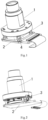
FIG. 1 is a structural view schematically showing a camera module according to an embodiment of the present disclosure; -
FIG. 2 is a structural view schematically showing a camera module according to a second embodiment of the present disclosure; -
FIG. 3 is a structural view schematically showing a circuit board according to the present disclosure; -
FIG. 4 is a structural view schematically showing a connector according to an embodiment inFIG. 2 ; -
FIG. 5 is a structural view schematically showing a connector according to a second embodiment inFIG. 2 ; and -
FIG. 6 is an exploded view schematically showing a camera module according to the present disclosure. - 1. lens; 2. circuit board; 3. connector; 4. solder; 21. thin plate; 22. steel sheet reinforced plate; 23. photosensitive chip; 24. electronic components; 25. flexible connection strip; 31. body portion; 32. connection pin.
- In order to more clearly illustrate the embodiments of the present disclosure or the technical solutions in the related art, drawings required to be used in the embodiments will be briefly described below. Obviously, the drawings in the following description show only some of the embodiments of the present disclosure, and those skilled in the art can obtain other drawings based on these drawings without creative efforts.
- When describing the embodiments of the present disclosure, the orientations or positional relationships described by the terms "longitudinal", "transverse", "upper", "lower", "front", "rear", "left", "right", "vertical", "horizontal", "top", "bottom", "inner" and "outer" are based on the orientations or positional relationships shown in the related drawings. These terms are merely used for the sake of facilitating describing the present disclosure and simplifying the description, and do not indicate or imply that the device or element as referred to must have a particular orientation, or must be constructed or operated in a particular orientation. Therefore, the above terms should not be construed as limiting the scope of the present disclosure.
- The present disclosure will be described in detail below with reference to the drawings and specific embodiments. It is impossible to describe all the embodiments exhaustively herein, but the embodiments of the present disclosure are not limited to those described below.
- The camera module of the present disclosure includes a lens 1, a
circuit board 2, and aconnector 3. As shown inFIGS. 1 and 2 , in an embodiment of the present disclosure, the lens 1 includes a lens barrel portion and a flange portion, and the flange portion is located on a lower side of the lens barrel portion and is connected to the lens barrel portion. In this embodiment, the lens barrel portion of the lens 1 is made of a metal material; for example, a material such as copper or aluminum may be used. This design solves the problem of poor consistency of the heat compensation amount caused by different thermal expansion coefficients when the split lens holder and lens are connected by thread and glue or by thread alone. - In the present disclosure, the flange portion of the lens 1 is connected to the
connector 3. As shown inFIG. 1 , according to an embodiment of the present disclosure, theconnector 3 is disposed between the lens 1 and thecircuit board 2. A connector mounting hole is disposed in the lens 1, theconnector 3 is mounted in the connector mounting hole, and the other end of theconnector 3 is welded to thecircuit board 2. - As shown in
FIGS. 2 ,5 and 6 , according to a second embodiment of the present disclosure, theconnector 3 includes abody portion 31 and connection pins 32. The connection pins 32 are disposed on a side of thebody portion 31 near thecircuit board 2. Thebody portion 31 is detachably connected to the lens 1, and the connection pins 32 and thecircuit board 2 are fixed by welding. - In the camera module of the present disclosure, the
connector 3 is disposed between the lens 1 and thecircuit board 2 so that the camera module of the present disclosure can be assembled more conveniently. The connection between the lens 1 and thecircuit board 2 is achieved by welding theconnector 3 and thecircuit board 2, which effectively avoids the defects caused by the connection between the lens and the circuit board implemented by glue in the related art, which is advantageous for ensuring the imaging quality of the camera module. - As shown in
FIG. 3 , thecircuit board 2 of the present disclosure includes athin plate 21 and a steel sheet reinforcedplate 22. In this embodiment, thethin plate 21 is located on an upper side, and the steel sheet reinforcedplate 22 is located on a lower side of thethin plate 21 and fitted and fixed to thethin plate 21. In the present disclosure, thethin plate 21 of thecircuit board 2 is provided with an image sensor, aphotosensitive chip 23,electronic components 24, and aflexible connection strip 25. Thecircuit board 2 of the present disclosure is further provided withpads 2a for carrying welding spots. Theconnector 3 and thecircuit board 2 of the present disclosure are fixedly connected by welding. Specifically, the connection pins 32 are welded and fixed to thepads 2a on thecircuit board 2 through asolder 4. - According to an embodiment of the present disclosure, the
pads 2a may be directly disposed on thethin plate 21. According to a second embodiment of the present disclosure, through holes may be provided in thethin plate 21 of thecircuit board 2, and thepads 2a are disposed in the through holes and fixed with the steel sheet reinforcedplate 22. That is, thepads 2a may be disposed on the steel sheet reinforcedplate 22. Both of the above ways can realize the welding of theconnector 3 or the connection pins 32 to thepads 2a. - The
circuit board 2 of the present disclosure includes athin plate 21 and a steel sheet reinforcedplate 22. By providing the steel sheet reinforcedplate 22, on one hand, a structural strength of thecircuit board 2 can be enhanced; and on the other hand, the steel sheet reinforcedplate 22 has the advantage of rapid heat dissipation, which can quickly take away the heat generated when thephotosensitive chip 23 works and ensure the uniform heat of theoverall circuit board 2 so that a deformation amount of thecircuit board 2 can be effectively controlled, thereby greatly improving the imaging quality of the camera module in a working state. - In the present disclosure, a thermal coefficient of the steel sheet reinforced
plate 22 is greater than a thermal coefficient of the connection pins 32. In addition, in this embodiment, theconnector 3 is made of carbon steel. With such an arrangement, during the welding process, heat conduction toward thelens 2 along theconnector 3 is slower, and heat conduction toward the steel sheet reinforcedplate 22 is faster, so that the heat generated in the working state of thecircuit board 2 is dissipated from the steel sheet reinforcedplate 22, and the rise in the temperature of thecircuit board 2 will not affect a temperature drift variation of the lens, so that the stability of the resolution is improved under a working condition of -40°C to 85°C, which is advantageous for ensuing the stability of the imaging quality so that the camera module of the present disclosure can be used under harsher environmental conditions for a wider range of applications. - As shown in
FIG. 4 , according to the first embodiment of the present disclosure, theconnector 3 is of an integrally formed configuration, that is, thebody portion 31 and the connection pins 32 of theconnector 3 are integrally formed. For example, theconnector 3 of the present disclosure may be manufactured by die-casting. - As shown in
FIG. 5 , in the second embodiment of the present disclosure, thebody portion 31 and the connection pins 32 of theconnector 3 are detachably connected, that is, the connection pins 32, as a separate assembly, need to be assembled to thebody portion 31 first. In this embodiment, threaded holes are provided in thebody portion 31, and the connection pins 32 are mounted in the threaded holes of thebody portion 31. - As shown in
FIG. 6 , the present disclosure also provides an assembly process of the camera module, which includes: a. mounting connection pins to the body portion to form a connector and then connecting the connector with the lens, or directly connecting a connector with the lens; b. focus-adjusting the lens 1 and the image sensor on thecircuit board 2; and c. fixing theconnector 3 to thecircuit board 2 by welding using thesolder 4. - Specifically, first, the lens 1, the
connector 3 and thecircuit board 2 that have passed the inspection are selected. If the selectedconnector 3 is a separate assembly, theconnector 3 is connected to the flange portion of the lens 1. If the selectedconnector 3 is not a separate assembly, the connection pins 32 are mounted to thebody portion 31 of the connector 3 (if an integrally formedconnector 3 is used, it is not necessary to separately mount the connection pins 32). After that, an automatic spot-soldering machine applies the solder 4 (which may be solder paste, solder ball, solder wire, etc.) at thepads 2a of thecircuit board 2. Subsequently, a relative position of the lens 1 to thecircuit board 2 is adjusted, the lens 1 and the image sensor on thecircuit board 2 are focus-adjusted, and the optical center, optical axis, and resolution are adjusted. After completion, the welding machine equipment is automatically turned on, and thesolder 4 at thepads 2a is heated and melted to achieve fixing. After cooling, the optical performance of the camera is tested. A test completion status is shown on an LED display, and the assembling of the lens 1 and thecircuit board 2 is completed. Then, other components may be assembled. - According to the second embodiment of the present disclosure, first, the lens 1, the
connector 3 and thecircuit board 2 that have passed the inspection are selected. If the selectedconnector 3 is a separate assembly, theconnector 3 is connected to the flange portion of the lens 1. If the selectedconnector 3 is not a separate assembly, the connection pins 32 are mounted to thebody portion 31 of the connector 3 (if an integrally formedconnector 3 is used, it is not necessary to separately mount the connection pins 32). Subsequently, a relative position of the lens 1 to thecircuit board 2 is adjusted, the lens 1 and the image sensor on thecircuit board 2 are focus-adjusted, and the optical center, optical axis, and resolution are adjusted. After the adjustment is completed, a solder feeding equipment applies solder wire or solder ball near gaps between thepads 2a and theconnector 3, and thesolder 4 is melted by the welding equipment and then drops into the gaps between thepads 2a and theconnector 3. After cooling, the optical performance of the camera is tested. A test completion status is shown on an LED display, and the assembling of the lens 1 and thecircuit board 2 is completed. Then, other components may be assembled. - In both the above two ways, the
connector 3 and the circuit board 22 (pads 2a) need to be plated before welding, which is advantageous for ensuring the firmness of the welding. Welding theconnector 3 and thepads 2a according to the above-mentioned two ways is advantageous for ensuring the focusing accuracy of the camera module of the present disclosure, thereby improving the imaging quality. - The above content is only an example of the specific solution of the present disclosure. For the devices and structures that are not described in detail, it should be understood that the general devices and general methods existing in the art are used to implement the present disclosure.
- The above described is only one embodiment of the present disclosure, and is not intended to limit the present disclosure. For those skilled in the art, various modifications and changes can be made to the present disclosure.
Claims (9)
- A camera module, comprising a lens (1) and a circuit board (2), wherein the camera module further comprises a connector (3), the connector (3) being located between the lens (1) and the circuit board (2) provided with pads (2a), the connector (3) comprises a body portion (31) and connection pins (32) connected to the body portion (31), the body portion (31) being detachably connected to the lens (1),
characterized in thatthe connection pins (32) are welded to the pads (2a) on circuit board (2),wherein the circuit board (2) comprises a thin plate (21), and a steel sheet reinforced plate (22) located on a lower side of the thin plate (21) and fitted and fixed to the thin plate (21), a thermal coefficient of the steel sheet reinforced plate (22) is greater than a thermal coefficient of the connection pins (32). - The camera module according to claim 1, wherein a connector mounting hole is disposed in the lens (1), and the connector (3) is mounted in the connector mounting hole.
- The camera module according to claim 1, wherein the body portion (31) and the connection pins (32) are of an integrally formed configuration.
- The camera module according to claim 1, wherein the connection pins (32) are detachably connected to the body portion (31).
- The camera module according to claim 1, wherein a material of the connector (3) is carbon steel.
- The camera module according to claim 1, wherein, the circuit board (2) is provided with an image sensor and electronic components
- The camera module according to claim 1, wherein the lens (1) is an integrated lens.
- An assembly process of the camera module according to claims 1 to 7, comprising:a. mounting connection pins to the body portion to form a connector and then connecting the connector with the lens, or directly connecting a connector with the lens;b. focus-adjusting the lens and the image sensor on the circuit board; andc. fixing the connector to the circuit board by welding using a solder.
- The assembly process according to claim 8, wherein prior to the step c, the connection pins and the circuit board need to be plated.
Applications Claiming Priority (2)
| Application Number | Priority Date | Filing Date | Title |
|---|---|---|---|
| CN201811209465.2A CN109068046B (en) | 2018-10-17 | 2018-10-17 | Camera module and assembly process |
| PCT/CN2018/118110 WO2020077750A1 (en) | 2018-10-17 | 2018-11-29 | Camera module and assembly process therefor |
Publications (3)
| Publication Number | Publication Date |
|---|---|
| EP3687153A1 EP3687153A1 (en) | 2020-07-29 |
| EP3687153A4 EP3687153A4 (en) | 2021-06-09 |
| EP3687153B1 true EP3687153B1 (en) | 2024-07-03 |
Family
ID=64764498
Family Applications (1)
| Application Number | Title | Priority Date | Filing Date |
|---|---|---|---|
| EP18932972.5A Active EP3687153B1 (en) | 2018-10-17 | 2018-11-29 | Camera module and assembly process therefor |
Country Status (3)
| Country | Link |
|---|---|
| EP (1) | EP3687153B1 (en) |
| CN (1) | CN109068046B (en) |
| WO (1) | WO2020077750A1 (en) |
Families Citing this family (7)
| Publication number | Priority date | Publication date | Assignee | Title |
|---|---|---|---|---|
| CN112291449B (en) * | 2019-07-25 | 2022-07-26 | 宁波舜宇光电信息有限公司 | Camera module, photosensitive assembly and manufacturing method thereof |
| CN110753170B (en) * | 2019-09-09 | 2024-08-30 | 浙江舜宇智领技术有限公司 | Camera module and assembling method |
| CN110830699A (en) * | 2019-11-28 | 2020-02-21 | 宁波为森智能传感技术有限公司 | Camera head |
| CN113347325B (en) * | 2020-03-02 | 2023-04-18 | 浙江宇视科技有限公司 | Imaging module and preparation method thereof |
| CN111854696A (en) * | 2020-07-02 | 2020-10-30 | 中国科学院光电技术研究所 | High reliability stepping frame type staring stereo imaging space camera and its realization method |
| CN112019729A (en) * | 2020-09-15 | 2020-12-01 | 湖南金康光电有限公司 | Camera module and electronic equipment |
| CN116506704B (en) * | 2023-04-12 | 2025-10-31 | 浙江大华技术股份有限公司 | Camera module and imaging system |
Family Cites Families (21)
| Publication number | Priority date | Publication date | Assignee | Title |
|---|---|---|---|---|
| JP4781252B2 (en) * | 2006-12-21 | 2011-09-28 | セイコープレシジョン株式会社 | Imaging device |
| CN101431609A (en) * | 2007-11-09 | 2009-05-13 | 鸿富锦精密工业(深圳)有限公司 | Imaging module group |
| CN201340473Y (en) * | 2008-12-24 | 2009-11-04 | 广州大凌实业有限公司 | Automatic focusing camera module |
| CN102419471A (en) * | 2010-09-27 | 2012-04-18 | 南京芒冠光电科技股份有限公司 | Short-focal-length lens |
| CN201947361U (en) * | 2010-12-06 | 2011-08-24 | 中兴通讯股份有限公司 | User terminal equipment with protective shield camera and camera thereof |
| CN102749790A (en) * | 2011-04-22 | 2012-10-24 | 易模塑科技(深圳)有限公司 | Automatic zoom lens module |
| JP5440559B2 (en) * | 2011-06-30 | 2014-03-12 | 株式会社ニコン | Lens barrel and imaging device |
| CN203480187U (en) * | 2013-09-02 | 2014-03-12 | 比亚迪股份有限公司 | Anti-shake camera module and mobile terminal using same |
| US9451138B2 (en) * | 2013-11-07 | 2016-09-20 | Magna Electronics Inc. | Camera for vehicle vision system |
| US9438782B2 (en) * | 2014-06-09 | 2016-09-06 | Arecont Vision, Llc. | Omnidirectional user configurable multi-camera housing |
| CN104967767A (en) * | 2015-07-03 | 2015-10-07 | 南昌欧菲光电技术有限公司 | Camera module and camera device |
| CN105116672A (en) * | 2015-10-12 | 2015-12-02 | 中山联合光电科技股份有限公司 | Novel lens connecting mechanism |
| CN106817515B (en) * | 2015-11-30 | 2020-07-24 | 宁波舜宇光电信息有限公司 | Camera module and structure and assembling method thereof |
| CN105721749B (en) * | 2016-02-24 | 2020-07-24 | 宁波舜宇光电信息有限公司 | Camera module, electric support and circuit board assembly thereof and manufacturing method |
| CN105704354B (en) * | 2016-03-12 | 2019-07-05 | 宁波舜宇光电信息有限公司 | Camera module, photosensitive assembly and manufacturing method thereof |
| US9647366B1 (en) * | 2016-04-12 | 2017-05-09 | Microsoft Technology Licensing, Llc | Connector shielding in an electronic device |
| KR101851146B1 (en) * | 2016-09-21 | 2018-04-24 | 현대자동차주식회사 | Camera for vehicle |
| CN106331455A (en) * | 2016-09-27 | 2017-01-11 | 华为技术有限公司 | Camera assembly and terminal |
| CN207283678U (en) * | 2017-11-01 | 2018-04-27 | 信利光电股份有限公司 | A kind of camera module and electronic equipment |
| CN207780450U (en) * | 2018-02-07 | 2018-08-28 | 杭州海康威视数字技术股份有限公司 | Lens mounting structure and camera |
| CN108668066A (en) * | 2018-08-01 | 2018-10-16 | 歌尔股份有限公司 | Camera module and its installation method |
-
2018
- 2018-10-17 CN CN201811209465.2A patent/CN109068046B/en active Active
- 2018-11-29 EP EP18932972.5A patent/EP3687153B1/en active Active
- 2018-11-29 WO PCT/CN2018/118110 patent/WO2020077750A1/en not_active Ceased
Also Published As
| Publication number | Publication date |
|---|---|
| EP3687153A1 (en) | 2020-07-29 |
| EP3687153A4 (en) | 2021-06-09 |
| WO2020077750A1 (en) | 2020-04-23 |
| CN109068046B (en) | 2020-05-15 |
| CN109068046A (en) | 2018-12-21 |
Similar Documents
| Publication | Publication Date | Title |
|---|---|---|
| EP3687153A1 (en) | Camera module and assembly process therefor | |
| US7633543B2 (en) | Solid state imaging apparatus | |
| US7710734B2 (en) | CFP mechanical platform | |
| CN110753170B (en) | Camera module and assembling method | |
| JP4889660B2 (en) | Imaging module | |
| US7311240B2 (en) | Electrical circuits with button plated contacts and assembly methods | |
| JP2015012211A (en) | Imaging unit and imaging device | |
| CN100538422C (en) | Double-sided adhesive tape assembly process for flexible circuit board mobile phone camera module lens | |
| US7530853B2 (en) | Socket and method for compensating for differing coefficients of thermal expansion | |
| JP2015146380A (en) | Imaging unit and imaging apparatus | |
| CN109348100B (en) | Camera module and assembling process thereof | |
| CN212460118U (en) | Optical module | |
| CN109040567B (en) | Camera module and assembly process | |
| CN219761142U (en) | Vehicle-mounted camera | |
| CN101652022B (en) | Positioning structure of photosensitive element | |
| US8072759B2 (en) | Electronic device | |
| CN210780975U (en) | Camera module and electronic equipment | |
| JPH05147264A (en) | Optical device | |
| KR20090060667A (en) | Digital camera | |
| JP2013078026A (en) | Imaging module | |
| CN220830558U (en) | Photosensitive plate assembly and camera module | |
| CN223309909U (en) | Vehicle-mounted camera module and vehicle | |
| CN120583306B (en) | A camera module | |
| CN121218015A (en) | A camera module, an electronic device, and a method for assembling the camera module. | |
| JP2013232732A (en) | Imaging device |
Legal Events
| Date | Code | Title | Description |
|---|---|---|---|
| STAA | Information on the status of an ep patent application or granted ep patent |
Free format text: STATUS: UNKNOWN |
|
| STAA | Information on the status of an ep patent application or granted ep patent |
Free format text: STATUS: THE INTERNATIONAL PUBLICATION HAS BEEN MADE |
|
| PUAI | Public reference made under article 153(3) epc to a published international application that has entered the european phase |
Free format text: ORIGINAL CODE: 0009012 |
|
| STAA | Information on the status of an ep patent application or granted ep patent |
Free format text: STATUS: REQUEST FOR EXAMINATION WAS MADE |
|
| 17P | Request for examination filed |
Effective date: 20200330 |
|
| AK | Designated contracting states |
Kind code of ref document: A1 Designated state(s): AL AT BE BG CH CY CZ DE DK EE ES FI FR GB GR HR HU IE IS IT LI LT LU LV MC MK MT NL NO PL PT RO RS SE SI SK SM TR |
|
| AX | Request for extension of the european patent |
Extension state: BA ME |
|
| RIN1 | Information on inventor provided before grant (corrected) |
Inventor name: NONG, KAIXUN Inventor name: ZHANG, BAOZHONG Inventor name: LIU, GAOFENG Inventor name: GU, YIWU Inventor name: HU, YUE |
|
| A4 | Supplementary search report drawn up and despatched |
Effective date: 20210507 |
|
| RIC1 | Information provided on ipc code assigned before grant |
Ipc: H04N 5/225 20060101AFI20210503BHEP |
|
| DAV | Request for validation of the european patent (deleted) | ||
| DAX | Request for extension of the european patent (deleted) | ||
| STAA | Information on the status of an ep patent application or granted ep patent |
Free format text: STATUS: EXAMINATION IS IN PROGRESS |
|
| 17Q | First examination report despatched |
Effective date: 20230213 |
|
| REG | Reference to a national code |
Ref country code: DE Ref legal event code: R079 Free format text: PREVIOUS MAIN CLASS: H04N0005225000 Ipc: H04N0023000000 Ref country code: DE Ref legal event code: R079 Ref document number: 602018071462 Country of ref document: DE Free format text: PREVIOUS MAIN CLASS: H04N0005225000 Ipc: H04N0023000000 |
|
| GRAP | Despatch of communication of intention to grant a patent |
Free format text: ORIGINAL CODE: EPIDOSNIGR1 |
|
| STAA | Information on the status of an ep patent application or granted ep patent |
Free format text: STATUS: GRANT OF PATENT IS INTENDED |
|
| RIC1 | Information provided on ipc code assigned before grant |
Ipc: H04N 23/00 20230101AFI20240213BHEP |
|
| INTG | Intention to grant announced |
Effective date: 20240314 |
|
| RIN1 | Information on inventor provided before grant (corrected) |
Inventor name: LIU, GAOFENG Inventor name: NONG, KAIXUN Inventor name: HU, YUE Inventor name: GU, YIWU Inventor name: ZHANG, BAOZHONG |
|
| GRAS | Grant fee paid |
Free format text: ORIGINAL CODE: EPIDOSNIGR3 |
|
| GRAA | (expected) grant |
Free format text: ORIGINAL CODE: 0009210 |
|
| STAA | Information on the status of an ep patent application or granted ep patent |
Free format text: STATUS: THE PATENT HAS BEEN GRANTED |
|
| RAP3 | Party data changed (applicant data changed or rights of an application transferred) |
Owner name: ZHEJIANG SUNNY SMARTLEAD TECHNOLOGIES CO., LTD. |
|
| AK | Designated contracting states |
Kind code of ref document: B1 Designated state(s): AL AT BE BG CH CY CZ DE DK EE ES FI FR GB GR HR HU IE IS IT LI LT LU LV MC MK MT NL NO PL PT RO RS SE SI SK SM TR |
|
| REG | Reference to a national code |
Ref country code: CH Ref legal event code: EP |
|
| REG | Reference to a national code |
Ref country code: DE Ref legal event code: R096 Ref document number: 602018071462 Country of ref document: DE |
|
| REG | Reference to a national code |
Ref country code: LT Ref legal event code: MG9D |
|
| REG | Reference to a national code |
Ref country code: NL Ref legal event code: MP Effective date: 20240703 |
|
| PG25 | Lapsed in a contracting state [announced via postgrant information from national office to epo] |
Ref country code: PT Free format text: LAPSE BECAUSE OF FAILURE TO SUBMIT A TRANSLATION OF THE DESCRIPTION OR TO PAY THE FEE WITHIN THE PRESCRIBED TIME-LIMIT Effective date: 20241104 |
|
| REG | Reference to a national code |
Ref country code: AT Ref legal event code: MK05 Ref document number: 1701008 Country of ref document: AT Kind code of ref document: T Effective date: 20240703 |
|
| PG25 | Lapsed in a contracting state [announced via postgrant information from national office to epo] |
Ref country code: NL Free format text: LAPSE BECAUSE OF FAILURE TO SUBMIT A TRANSLATION OF THE DESCRIPTION OR TO PAY THE FEE WITHIN THE PRESCRIBED TIME-LIMIT Effective date: 20240703 |
|
| PG25 | Lapsed in a contracting state [announced via postgrant information from national office to epo] |
Ref country code: PT Free format text: LAPSE BECAUSE OF FAILURE TO SUBMIT A TRANSLATION OF THE DESCRIPTION OR TO PAY THE FEE WITHIN THE PRESCRIBED TIME-LIMIT Effective date: 20241104 Ref country code: NL Free format text: LAPSE BECAUSE OF FAILURE TO SUBMIT A TRANSLATION OF THE DESCRIPTION OR TO PAY THE FEE WITHIN THE PRESCRIBED TIME-LIMIT Effective date: 20240703 |
|
| PG25 | Lapsed in a contracting state [announced via postgrant information from national office to epo] |
Ref country code: NO Free format text: LAPSE BECAUSE OF FAILURE TO SUBMIT A TRANSLATION OF THE DESCRIPTION OR TO PAY THE FEE WITHIN THE PRESCRIBED TIME-LIMIT Effective date: 20241003 |
|
| PG25 | Lapsed in a contracting state [announced via postgrant information from national office to epo] |
Ref country code: PL Free format text: LAPSE BECAUSE OF FAILURE TO SUBMIT A TRANSLATION OF THE DESCRIPTION OR TO PAY THE FEE WITHIN THE PRESCRIBED TIME-LIMIT Effective date: 20240703 Ref country code: GR Free format text: LAPSE BECAUSE OF FAILURE TO SUBMIT A TRANSLATION OF THE DESCRIPTION OR TO PAY THE FEE WITHIN THE PRESCRIBED TIME-LIMIT Effective date: 20241004 Ref country code: FI Free format text: LAPSE BECAUSE OF FAILURE TO SUBMIT A TRANSLATION OF THE DESCRIPTION OR TO PAY THE FEE WITHIN THE PRESCRIBED TIME-LIMIT Effective date: 20240703 |
|
| PG25 | Lapsed in a contracting state [announced via postgrant information from national office to epo] |
Ref country code: BG Free format text: LAPSE BECAUSE OF FAILURE TO SUBMIT A TRANSLATION OF THE DESCRIPTION OR TO PAY THE FEE WITHIN THE PRESCRIBED TIME-LIMIT Effective date: 20240703 |
|
| PG25 | Lapsed in a contracting state [announced via postgrant information from national office to epo] |
Ref country code: LV Free format text: LAPSE BECAUSE OF FAILURE TO SUBMIT A TRANSLATION OF THE DESCRIPTION OR TO PAY THE FEE WITHIN THE PRESCRIBED TIME-LIMIT Effective date: 20240703 |
|
| PG25 | Lapsed in a contracting state [announced via postgrant information from national office to epo] |
Ref country code: IS Free format text: LAPSE BECAUSE OF FAILURE TO SUBMIT A TRANSLATION OF THE DESCRIPTION OR TO PAY THE FEE WITHIN THE PRESCRIBED TIME-LIMIT Effective date: 20241103 Ref country code: AT Free format text: LAPSE BECAUSE OF FAILURE TO SUBMIT A TRANSLATION OF THE DESCRIPTION OR TO PAY THE FEE WITHIN THE PRESCRIBED TIME-LIMIT Effective date: 20240703 |
|
| PG25 | Lapsed in a contracting state [announced via postgrant information from national office to epo] |
Ref country code: HR Free format text: LAPSE BECAUSE OF FAILURE TO SUBMIT A TRANSLATION OF THE DESCRIPTION OR TO PAY THE FEE WITHIN THE PRESCRIBED TIME-LIMIT Effective date: 20240703 Ref country code: CZ Free format text: LAPSE BECAUSE OF FAILURE TO SUBMIT A TRANSLATION OF THE DESCRIPTION OR TO PAY THE FEE WITHIN THE PRESCRIBED TIME-LIMIT Effective date: 20240703 |
|
| PG25 | Lapsed in a contracting state [announced via postgrant information from national office to epo] |
Ref country code: ES Free format text: LAPSE BECAUSE OF FAILURE TO SUBMIT A TRANSLATION OF THE DESCRIPTION OR TO PAY THE FEE WITHIN THE PRESCRIBED TIME-LIMIT Effective date: 20240703 Ref country code: RS Free format text: LAPSE BECAUSE OF FAILURE TO SUBMIT A TRANSLATION OF THE DESCRIPTION OR TO PAY THE FEE WITHIN THE PRESCRIBED TIME-LIMIT Effective date: 20241003 |
|
| PG25 | Lapsed in a contracting state [announced via postgrant information from national office to epo] |
Ref country code: RS Free format text: LAPSE BECAUSE OF FAILURE TO SUBMIT A TRANSLATION OF THE DESCRIPTION OR TO PAY THE FEE WITHIN THE PRESCRIBED TIME-LIMIT Effective date: 20241003 Ref country code: PL Free format text: LAPSE BECAUSE OF FAILURE TO SUBMIT A TRANSLATION OF THE DESCRIPTION OR TO PAY THE FEE WITHIN THE PRESCRIBED TIME-LIMIT Effective date: 20240703 Ref country code: NO Free format text: LAPSE BECAUSE OF FAILURE TO SUBMIT A TRANSLATION OF THE DESCRIPTION OR TO PAY THE FEE WITHIN THE PRESCRIBED TIME-LIMIT Effective date: 20241003 Ref country code: LV Free format text: LAPSE BECAUSE OF FAILURE TO SUBMIT A TRANSLATION OF THE DESCRIPTION OR TO PAY THE FEE WITHIN THE PRESCRIBED TIME-LIMIT Effective date: 20240703 Ref country code: IS Free format text: LAPSE BECAUSE OF FAILURE TO SUBMIT A TRANSLATION OF THE DESCRIPTION OR TO PAY THE FEE WITHIN THE PRESCRIBED TIME-LIMIT Effective date: 20241103 Ref country code: HR Free format text: LAPSE BECAUSE OF FAILURE TO SUBMIT A TRANSLATION OF THE DESCRIPTION OR TO PAY THE FEE WITHIN THE PRESCRIBED TIME-LIMIT Effective date: 20240703 Ref country code: GR Free format text: LAPSE BECAUSE OF FAILURE TO SUBMIT A TRANSLATION OF THE DESCRIPTION OR TO PAY THE FEE WITHIN THE PRESCRIBED TIME-LIMIT Effective date: 20241004 Ref country code: FI Free format text: LAPSE BECAUSE OF FAILURE TO SUBMIT A TRANSLATION OF THE DESCRIPTION OR TO PAY THE FEE WITHIN THE PRESCRIBED TIME-LIMIT Effective date: 20240703 Ref country code: ES Free format text: LAPSE BECAUSE OF FAILURE TO SUBMIT A TRANSLATION OF THE DESCRIPTION OR TO PAY THE FEE WITHIN THE PRESCRIBED TIME-LIMIT Effective date: 20240703 Ref country code: CZ Free format text: LAPSE BECAUSE OF FAILURE TO SUBMIT A TRANSLATION OF THE DESCRIPTION OR TO PAY THE FEE WITHIN THE PRESCRIBED TIME-LIMIT Effective date: 20240703 Ref country code: BG Free format text: LAPSE BECAUSE OF FAILURE TO SUBMIT A TRANSLATION OF THE DESCRIPTION OR TO PAY THE FEE WITHIN THE PRESCRIBED TIME-LIMIT Effective date: 20240703 Ref country code: AT Free format text: LAPSE BECAUSE OF FAILURE TO SUBMIT A TRANSLATION OF THE DESCRIPTION OR TO PAY THE FEE WITHIN THE PRESCRIBED TIME-LIMIT Effective date: 20240703 |
|
| REG | Reference to a national code |
Ref country code: DE Ref legal event code: R097 Ref document number: 602018071462 Country of ref document: DE |
|
| PG25 | Lapsed in a contracting state [announced via postgrant information from national office to epo] |
Ref country code: SM Free format text: LAPSE BECAUSE OF FAILURE TO SUBMIT A TRANSLATION OF THE DESCRIPTION OR TO PAY THE FEE WITHIN THE PRESCRIBED TIME-LIMIT Effective date: 20240703 Ref country code: DK Free format text: LAPSE BECAUSE OF FAILURE TO SUBMIT A TRANSLATION OF THE DESCRIPTION OR TO PAY THE FEE WITHIN THE PRESCRIBED TIME-LIMIT Effective date: 20240703 Ref country code: RO Free format text: LAPSE BECAUSE OF FAILURE TO SUBMIT A TRANSLATION OF THE DESCRIPTION OR TO PAY THE FEE WITHIN THE PRESCRIBED TIME-LIMIT Effective date: 20240703 |
|
| PG25 | Lapsed in a contracting state [announced via postgrant information from national office to epo] |
Ref country code: EE Free format text: LAPSE BECAUSE OF FAILURE TO SUBMIT A TRANSLATION OF THE DESCRIPTION OR TO PAY THE FEE WITHIN THE PRESCRIBED TIME-LIMIT Effective date: 20240703 |
|
| PG25 | Lapsed in a contracting state [announced via postgrant information from national office to epo] |
Ref country code: IT Free format text: LAPSE BECAUSE OF FAILURE TO SUBMIT A TRANSLATION OF THE DESCRIPTION OR TO PAY THE FEE WITHIN THE PRESCRIBED TIME-LIMIT Effective date: 20240703 Ref country code: SK Free format text: LAPSE BECAUSE OF FAILURE TO SUBMIT A TRANSLATION OF THE DESCRIPTION OR TO PAY THE FEE WITHIN THE PRESCRIBED TIME-LIMIT Effective date: 20240703 |
|
| PLBE | No opposition filed within time limit |
Free format text: ORIGINAL CODE: 0009261 |
|
| STAA | Information on the status of an ep patent application or granted ep patent |
Free format text: STATUS: NO OPPOSITION FILED WITHIN TIME LIMIT |
|
| 26N | No opposition filed |
Effective date: 20250404 |
|
| REG | Reference to a national code |
Ref country code: CH Ref legal event code: PL |
|
| PG25 | Lapsed in a contracting state [announced via postgrant information from national office to epo] |
Ref country code: MC Free format text: LAPSE BECAUSE OF FAILURE TO SUBMIT A TRANSLATION OF THE DESCRIPTION OR TO PAY THE FEE WITHIN THE PRESCRIBED TIME-LIMIT Effective date: 20240703 |
|
| PG25 | Lapsed in a contracting state [announced via postgrant information from national office to epo] |
Ref country code: LU Free format text: LAPSE BECAUSE OF NON-PAYMENT OF DUE FEES Effective date: 20241129 |
|
| REG | Reference to a national code |
Ref country code: CH Ref legal event code: PL |
|
| PG25 | Lapsed in a contracting state [announced via postgrant information from national office to epo] |
Ref country code: CH Free format text: LAPSE BECAUSE OF NON-PAYMENT OF DUE FEES Effective date: 20241130 |
|
| REG | Reference to a national code |
Ref country code: BE Ref legal event code: MM Effective date: 20241130 |
|
| PG25 | Lapsed in a contracting state [announced via postgrant information from national office to epo] |
Ref country code: SE Free format text: LAPSE BECAUSE OF FAILURE TO SUBMIT A TRANSLATION OF THE DESCRIPTION OR TO PAY THE FEE WITHIN THE PRESCRIBED TIME-LIMIT Effective date: 20240703 |
|
| PG25 | Lapsed in a contracting state [announced via postgrant information from national office to epo] |
Ref country code: BE Free format text: LAPSE BECAUSE OF NON-PAYMENT OF DUE FEES Effective date: 20241130 |
|
| PG25 | Lapsed in a contracting state [announced via postgrant information from national office to epo] |
Ref country code: IE Free format text: LAPSE BECAUSE OF NON-PAYMENT OF DUE FEES Effective date: 20241129 |
|
| PGFP | Annual fee paid to national office [announced via postgrant information from national office to epo] |
Ref country code: DE Payment date: 20251106 Year of fee payment: 8 |
|
| PGFP | Annual fee paid to national office [announced via postgrant information from national office to epo] |
Ref country code: GB Payment date: 20251120 Year of fee payment: 8 |
|
| PGFP | Annual fee paid to national office [announced via postgrant information from national office to epo] |
Ref country code: FR Payment date: 20251120 Year of fee payment: 8 |
|
| PG25 | Lapsed in a contracting state [announced via postgrant information from national office to epo] |
Ref country code: HU Free format text: LAPSE BECAUSE OF FAILURE TO SUBMIT A TRANSLATION OF THE DESCRIPTION OR TO PAY THE FEE WITHIN THE PRESCRIBED TIME-LIMIT; INVALID AB INITIO Effective date: 20181129 |
|
| PG25 | Lapsed in a contracting state [announced via postgrant information from national office to epo] |
Ref country code: CY Free format text: LAPSE BECAUSE OF FAILURE TO SUBMIT A TRANSLATION OF THE DESCRIPTION OR TO PAY THE FEE WITHIN THE PRESCRIBED TIME-LIMIT; INVALID AB INITIO Effective date: 20181129 |