EP3686928A1 - A semiconductor device and corresponding method of manufacture - Google Patents
A semiconductor device and corresponding method of manufacture Download PDFInfo
- Publication number
- EP3686928A1 EP3686928A1 EP20151379.3A EP20151379A EP3686928A1 EP 3686928 A1 EP3686928 A1 EP 3686928A1 EP 20151379 A EP20151379 A EP 20151379A EP 3686928 A1 EP3686928 A1 EP 3686928A1
- Authority
- EP
- European Patent Office
- Prior art keywords
- mounting portion
- chip mounting
- lead
- plane
- electrically
- Prior art date
- Legal status (The legal status is an assumption and is not a legal conclusion. Google has not performed a legal analysis and makes no representation as to the accuracy of the status listed.)
- Granted
Links
Images



Classifications
-
- H—ELECTRICITY
- H10—SEMICONDUCTOR DEVICES; ELECTRIC SOLID-STATE DEVICES NOT OTHERWISE PROVIDED FOR
- H10W—GENERIC PACKAGES, INTERCONNECTIONS, CONNECTORS OR OTHER CONSTRUCTIONAL DETAILS OF DEVICES COVERED BY CLASS H10
- H10W70/00—Package substrates; Interposers; Redistribution layers [RDL]
- H10W70/01—Manufacture or treatment
- H10W70/04—Manufacture or treatment of leadframes
-
- H—ELECTRICITY
- H10—SEMICONDUCTOR DEVICES; ELECTRIC SOLID-STATE DEVICES NOT OTHERWISE PROVIDED FOR
- H10W—GENERIC PACKAGES, INTERCONNECTIONS, CONNECTORS OR OTHER CONSTRUCTIONAL DETAILS OF DEVICES COVERED BY CLASS H10
- H10W70/00—Package substrates; Interposers; Redistribution layers [RDL]
- H10W70/01—Manufacture or treatment
- H10W70/04—Manufacture or treatment of leadframes
- H10W70/041—Connecting or disconnecting interconnections to or from leadframes, e.g. connecting bond wires or bumps
-
- H—ELECTRICITY
- H10—SEMICONDUCTOR DEVICES; ELECTRIC SOLID-STATE DEVICES NOT OTHERWISE PROVIDED FOR
- H10W—GENERIC PACKAGES, INTERCONNECTIONS, CONNECTORS OR OTHER CONSTRUCTIONAL DETAILS OF DEVICES COVERED BY CLASS H10
- H10W70/00—Package substrates; Interposers; Redistribution layers [RDL]
- H10W70/40—Leadframes
- H10W70/411—Chip-supporting parts, e.g. die pads
-
- H—ELECTRICITY
- H10—SEMICONDUCTOR DEVICES; ELECTRIC SOLID-STATE DEVICES NOT OTHERWISE PROVIDED FOR
- H10W—GENERIC PACKAGES, INTERCONNECTIONS, CONNECTORS OR OTHER CONSTRUCTIONAL DETAILS OF DEVICES COVERED BY CLASS H10
- H10W70/00—Package substrates; Interposers; Redistribution layers [RDL]
- H10W70/40—Leadframes
- H10W70/421—Shapes or dispositions
- H10W70/424—Cross-sectional shapes
-
- H—ELECTRICITY
- H10—SEMICONDUCTOR DEVICES; ELECTRIC SOLID-STATE DEVICES NOT OTHERWISE PROVIDED FOR
- H10W—GENERIC PACKAGES, INTERCONNECTIONS, CONNECTORS OR OTHER CONSTRUCTIONAL DETAILS OF DEVICES COVERED BY CLASS H10
- H10W70/00—Package substrates; Interposers; Redistribution layers [RDL]
- H10W70/40—Leadframes
- H10W70/464—Additional interconnections in combination with leadframes
-
- H—ELECTRICITY
- H10—SEMICONDUCTOR DEVICES; ELECTRIC SOLID-STATE DEVICES NOT OTHERWISE PROVIDED FOR
- H10W—GENERIC PACKAGES, INTERCONNECTIONS, CONNECTORS OR OTHER CONSTRUCTIONAL DETAILS OF DEVICES COVERED BY CLASS H10
- H10W70/00—Package substrates; Interposers; Redistribution layers [RDL]
- H10W70/40—Leadframes
- H10W70/464—Additional interconnections in combination with leadframes
- H10W70/465—Bumps or wires
-
- H—ELECTRICITY
- H10—SEMICONDUCTOR DEVICES; ELECTRIC SOLID-STATE DEVICES NOT OTHERWISE PROVIDED FOR
- H10W—GENERIC PACKAGES, INTERCONNECTIONS, CONNECTORS OR OTHER CONSTRUCTIONAL DETAILS OF DEVICES COVERED BY CLASS H10
- H10W70/00—Package substrates; Interposers; Redistribution layers [RDL]
- H10W70/40—Leadframes
- H10W70/475—Capacitors in combination with leadframes
-
- H—ELECTRICITY
- H10—SEMICONDUCTOR DEVICES; ELECTRIC SOLID-STATE DEVICES NOT OTHERWISE PROVIDED FOR
- H10W—GENERIC PACKAGES, INTERCONNECTIONS, CONNECTORS OR OTHER CONSTRUCTIONAL DETAILS OF DEVICES COVERED BY CLASS H10
- H10W90/00—Package configurations
- H10W90/811—Multiple chips on leadframes
-
- H—ELECTRICITY
- H10—SEMICONDUCTOR DEVICES; ELECTRIC SOLID-STATE DEVICES NOT OTHERWISE PROVIDED FOR
- H10W—GENERIC PACKAGES, INTERCONNECTIONS, CONNECTORS OR OTHER CONSTRUCTIONAL DETAILS OF DEVICES COVERED BY CLASS H10
- H10W72/00—Interconnections or connectors in packages
- H10W72/071—Connecting or disconnecting
- H10W72/073—Connecting or disconnecting of die-attach connectors
-
- H—ELECTRICITY
- H10—SEMICONDUCTOR DEVICES; ELECTRIC SOLID-STATE DEVICES NOT OTHERWISE PROVIDED FOR
- H10W—GENERIC PACKAGES, INTERCONNECTIONS, CONNECTORS OR OTHER CONSTRUCTIONAL DETAILS OF DEVICES COVERED BY CLASS H10
- H10W72/00—Interconnections or connectors in packages
- H10W72/071—Connecting or disconnecting
- H10W72/075—Connecting or disconnecting of bond wires
-
- H—ELECTRICITY
- H10—SEMICONDUCTOR DEVICES; ELECTRIC SOLID-STATE DEVICES NOT OTHERWISE PROVIDED FOR
- H10W—GENERIC PACKAGES, INTERCONNECTIONS, CONNECTORS OR OTHER CONSTRUCTIONAL DETAILS OF DEVICES COVERED BY CLASS H10
- H10W72/00—Interconnections or connectors in packages
- H10W72/50—Bond wires
- H10W72/531—Shapes of wire connectors
- H10W72/536—Shapes of wire connectors the connected ends being ball-shaped
-
- H—ELECTRICITY
- H10—SEMICONDUCTOR DEVICES; ELECTRIC SOLID-STATE DEVICES NOT OTHERWISE PROVIDED FOR
- H10W—GENERIC PACKAGES, INTERCONNECTIONS, CONNECTORS OR OTHER CONSTRUCTIONAL DETAILS OF DEVICES COVERED BY CLASS H10
- H10W72/00—Interconnections or connectors in packages
- H10W72/50—Bond wires
- H10W72/531—Shapes of wire connectors
- H10W72/5363—Shapes of wire connectors the connected ends being wedge-shaped
-
- H—ELECTRICITY
- H10—SEMICONDUCTOR DEVICES; ELECTRIC SOLID-STATE DEVICES NOT OTHERWISE PROVIDED FOR
- H10W—GENERIC PACKAGES, INTERCONNECTIONS, CONNECTORS OR OTHER CONSTRUCTIONAL DETAILS OF DEVICES COVERED BY CLASS H10
- H10W72/00—Interconnections or connectors in packages
- H10W72/851—Dispositions of multiple connectors or interconnections
- H10W72/874—On different surfaces
- H10W72/884—Die-attach connectors and bond wires
Definitions
- the description relates to semiconductor devices.
- One or more embodiments may apply, for instance, to integrated circuits (ICs).
- ICs integrated circuits
- PCBs printed circuit boards
- IC devices which may be arranged in plastic/ceramic packages
- passive components passive components
- connectors and so on.
- SiP system in package
- SMD surface mount device
- LF leadframe
- An object of one or more embodiments is to contribute in providing such improved solutions.
- That object may be achieved by means of a semiconductor device having the features set forth in the claims that follow.
- One or more embodiments may relate to a corresponding method of manufacturing semiconductor devices.
- One or more embodiments may comprise component integrated in a package (a SMD for instance) mounted "vertically" on a die-pad abutted against and coupled to a dedicated lead of the leadframe.
- a SMD for instance
- One or more embodiments were found to provide up to 40% impedance reduction in a capacitive component above 30 MHz.
- One or more embodiments may provide a leadframe package including a two-terminal SMD mounted/coupled vertically on a die-pad and having its other terminal electrically coupled through a lead or a wire, for instance.
- references to "an embodiment” or “one embodiment” in the framework of the present description is intended to indicate that a particular configuration, structure, or characteristic described in relation to the embodiment is comprised in at least one embodiment.
- phrases such as “in an embodiment” or “in one embodiment” that may be present in one or more points of the present description do not necessarily refer to one and the same embodiment.
- particular conformations, structures, or characteristics may be combined in any adequate way in one or more embodiments.
- Such solutions may suffer from various drawbacks related to poor electrical performance related to long connection formations as provided for coupling a (passive, for instance) electrical component to an integrated circuit (an application-specific integrated circuit or ASIC, for instance), with intermediate elements or substrate parts possibly intervening.
- Figure 1 is exemplary of a portion of a semiconductor product package including one or more leads 10 in a leadframe (not visible in its entirety) having their inner ends facing and at least partially overlapping a portion 12 of the package (a so-called die-pad or slug) onto which one or more semiconductor chips or dice 14 are intended to be mounted (in a manner known to those of skill in the art).
- Reference 16 denotes an electrical component (a passive component such as a decoupling capacitor, for instance) arranged bridge-like between one (electrically-conductive) lead 10 and the (electrically-conductive) pad or slug 12 to provide electrical coupling therebetween.
- an electrical component a passive component such as a decoupling capacitor, for instance
- the lead 10 and the pad or slug 12 may be regarded as extending in respective - at least approximately parallel - (e.g. median) planes X10 and X12 which are mutually offset with the component 16 extending between these two planes.
- such electrical coupling can be provided - as discussed in the following - via electrically-conductive masses 18 and 20.
- a SMD capacitor such as a EIA SIZE 0201 (length x width 0.6 x 0.3 mm) capacitor or a EIA SIZE 0402 (length x width 1.0 x 0.5 mm) capacitor may be exemplary of a component such as the component 16.
- the component 16 may be of elongate form or shape, namely a form long in comparison to its width, for instance a length twice the width as in the case of the EIA SIZE 0201 or EIA SIZE 0402 capacitors mentioned previously by way of example.
- the component 16 may thus be mounted bridge-like between the lead 10 and the pad or slug 12 with a longitudinal axis X16 (that is the axis along the direction of longer or longest extension of the component 16) arranged transverse the pad or slug 12.
- the component 16 may be mounted with the longitudinal axis X16 orthogonal a plane of extension X12 of the pad or slug 12. For instance, by assuming that the pad or slug 12 may be regarded as lying in a horizontal plane X12, the elongate component 16 may be arranged with its axis X16 arranged vertically.
- Figure 3A shows a leadframe provided (in a manner known to those of skill in the art) with one or more leads 10 having a (inner) end facing a corresponding (peripheral, for instance) portion of the pad or slug 12 with a separation gap 22 therebetween.
- the inner end of the lead 10 may overlap (that is, protrudes above) the portion of the pad or slug 12. I will be otherwise appreciated (see Figures 7 and 8 discussed in the following, for instance) that such an overlap is not mandatory feature.
- FIG. 3A a semiconductor chip or die 14 is shown already attached (in any manner known to those of skill in the art) onto the pad or slug 12.
- Figure 3B is exemplary of an act of providing onto the die-pad or slug 12 a (first) electrically-conductive mass (vertically) aligned with the end of the lead 10 protruding over the pad or slug 12.
- the mass 18 may comprise preform or solder material applied onto the pad or slug 12 possibly after an agent (or flux) has been dispensed to facilitate firm adhesion of the mass 18 to the pad or slug 12.
- Figure 3C is exemplary of a component 16 being placed onto the mass 18 which, as discussed previously, may involve placing an elongate component 16 "vertically", that is with its main dimension X16 extending transverse to the pad or slug 12.
- Figure 3D is exemplary of a (second) mass of electrically-conductive material 20 being provided between the (upper) termination of the component 16 and the inner tip of the lead 10.
- the mass 20 may include preform or solder material.
- the act exemplified in Figure 3D may also include solder reflow and agent (or flux) cleaning.
- Figure 3E is exemplary of the possible provision of (otherwise conventional) wire or ribbon bonding 24 to provide electrical coupling of the lead 10 with corresponding die pads (see reference 24a) at the front or upper surface of the semiconductor chip or die 14.
- the sequence of acts exemplified in Figures 3A to 3E is not mandatory.
- the semiconductor die or chip 14 may be attached to the pad or slug 12 - after - the component 16 has been arranged bridge-like across the gap 22 between the lead 10 and the pad or slug 12.
- Figures 1 and 2 are exemplary of the possibility for the component 16 to extend bridge-like between the chip mounting portion 12 and a lateral surface of the lead 10 in abutment with that lateral surface, thus extending sidewise of the lead 10 rather than being sandwiched between the lead 10 and the pad or slug 12.
- the lead 10 may exhibit a lateral surface, such as a "vertical" end surface transverse the plane X10 and/or X12, so that the component 16 can be abutted at its end (here an upper end) facing the lead 10 against the lateral surface of the lead 10.
- this may also facilitate placement from the top of the leadframe and/or using a component 16 having a length longer than the distance between the lead 10 and the pad or slug 12 as measured transverse (orthogonal) to the planes X10 and X12.
- the lead 10 may be a power lead.
- a rigid joint to the pad or slug 12 as created via the electrical component 16 may thus be exposed to the risk of breaking as a result of the lead being clamped (at a clamping area A as exemplified in Figure 4 ) at wire bonding.
- such an issue may be addressed by providing a physical connection (for instance a bridge contact as exemplified as 100 in Figure 5 ) between the (power) lead 10 to which the component 16 is coupled and at least one adjacent lead 10 having to such rigid joint to the pad or slug 12.
- a physical connection for instance a bridge contact as exemplified as 100 in Figure 5
- One or more embodiments may contemplate modifying the clamping foot design intended to act at the clamping area A by providing a gap therein as exemplified at 102 in Figure 5 .
- a local relief can thus be provided at the lead 10 to which the component 16 is coupled by avoiding applying clamping force thereto, while - as exemplified in Figure 5 - a (power) wire coupling to the chip of die 12 may be provided for the power lead 10 to which the component 16 is coupled via an adjacent lead 10 (on the right, in Figure 5 ) physically connected thereto (via the bridge contact 100, for instance).
- Figures 6A and 6B is exemplary of a stamping process applied to a raw base material (e.g. copper in reel form) 1000 for the leadframe.
- a raw base material e.g. copper in reel form
- Stamping tool flexibility in such a process may facilitate (possibly during leadframe manufacturing by a supplier) adding/removing punches and changing their positions in order to provided a pin-to-pin (lead-to-lead) electrical connection (100, for instance) where desired.
- Figure 6B is exemplary of a stamping process via a stamping tool ST resulting in a plurality of leads 10 being physically (and also electrically) coupled to one another via bridges 100 as exemplified in Figure 6C .
- a stamping process as exemplified herein may include a further act of punching away (as exemplified at P in Figure 6D ) those pin-to-pin connection which may not be desired for a certain application.
- the possibility of using a same lead 10 as a power lead for a plurality of semiconductor products (ICs, for instance) may facilitate adopting a standardized location of physical connection thus facilitating leadframe design standardization.
- Figures 7 and 8 exemplify one or more embodiments applied to arrangements (such as QFP packages - QFP being an acronym for Quad Flat Package) including leads 10 facing a pad or slug 12 and defining a gap 22 therewith without protruding above the pad or slug 12.
- arrangements such as QFP packages - QFP being an acronym for Quad Flat Package
- the lead 10 and the pad or slug 12 may be regarded as extending in respective (at least approximately parallel) planes X10 and X12 (e.g. median planes of the lead 10 and the pad or slug 12, respectively) which are mutually offset with the component 16 extending between these two planes.
- planes X10 and X12 e.g. median planes of the lead 10 and the pad or slug 12, respectively
- the electrically-conductive mass 20 discussed in the foregoing may be replaced by wire (or possibly ribbon) bonding 200 which electrically couples to the lead 10 the termination of the component 16 opposite to the pad or slug 12.
- Such wire or ribbon bonding of the component 16 to the lead 10 may be:
- One or more embodiments as exemplified in Figures 7 and 8 may retain the advantage of arranging an elongate component 16 such as an EIA SIZE 0201 or EIA SIZE 0402 capacitor transverse to the pad or slug 12 (vertical, for instance) thus reducing the footprint of the component 16 on the pad or slug 12.
- an elongate component 16 such as an EIA SIZE 0201 or EIA SIZE 0402 capacitor transverse to the pad or slug 12 (vertical, for instance) thus reducing the footprint of the component 16 on the pad or slug 12.
- One or more embodiments as exemplified in Figures 7 and 8 are again exemplary of the possibility for the component 16 to have a length longer than the distance between the lead 10 and the pad or slug 12, as measured transverse (orthogonal) to the planes X10 and X12, as a result of extending sidewise of the lead 10.
- the diagram of Figure 9 is exemplary of the impedance (Ohm) measured over a frequency range between 0.001 and 1.000 GHz for a 0201 SMD capacitor having a nominal capacitance value of 10 nF.
- the impedance behavior for a capacitor assembly according to embodiments of the present description as (illustrated by the chained line in Figure 9 ) shows an improvement in excess of 40% in comparison with the impedance behavior for a conventional capacitor assembly (shown in continuous line) over the whole of the frequency range above the frequency where the lowest impedance is measured.
- One or more embodiments may thus provide an optimized electrical connection from a ground electrode (as provided by the pad or slug 12) to the back side of the die 14 achieved through a slug and not through a wire, while also exhibiting a shorter wire connection from the leads 10 (for instance a power lead) to the die 14.
- One or more embodiments may facilitate reducing (notionally halving) the number of dedicated power supply pins in a semiconductor device such as an integrated circuit in comparison with conventional planar SMD assembly, while also facilitating leadframe design standardization as discussed previously.
- a device as exemplified herein may comprise:
- a device as exemplified herein may comprise an elongate electrical component extending along a longitudinal axis (for instance, X16), the electrical component arranged on the chip mounting portion with said longitudinal axis transverse (for instance, orthogonal to) the second plane.
- a longitudinal axis for instance, X16
- the electrical component arranged on the chip mounting portion with said longitudinal axis transverse (for instance, orthogonal to) the second plane.
- a device as exemplified herein may comprise:
- the first electrically-conductive formation may comprise electrically-conductive material electrically and mechanically coupling the electrical component and the chip mounting portion.
- said at least one lead may be arranged facing and at least partially overlapping the chip mounting portion (see, for instance, Figure 2 ), the electrical component extending bridge-like between the chip mounting portion and the at least one lead arranged facing the chip mounting portion.
- the second electrically-conductive formation may comprise electrically-conductive material electrically and mechanically (see, for instance 20 in Figure 2 ) coupling the electrical component to the at least one lead arranged facing and at least partially overlapping the chip mounting portion.
- the at least one second electrically-conductive formation may comprise wire-like (wire or ribbon) material (for instance, 200 or 200, 24) electrically coupling the electrical component to the at least one lead arranged facing the chip mounting portion either directly (see, for instance 200 in Figure 7 ) or (see, for instance 200, 24 in Figure 8 ) via the at least one semiconductor chip on the chip mounting portion.
- wire-like (wire or ribbon) material for instance, 200 or 200, 24
- the electrical component (for instance, 16) may extend sidewise of the at least one lead between the chip mounting portion and a lateral surface of the at least one lead in abutment with said lateral surface.
- the electrical component may have a length longer than the distance between said chip mounting portion and said at least one lead transverse (orthogonal to, for instance) said first plane and said second plane.
- a device as exemplified herein may comprise:
- a method of manufacturing a device as exemplified herein may comprise:
- a method as exemplified herein may comprise providing wire-like material (for instance, 24 in Figures 4 and 5 ) electrically coupling the leadframe to the at least one semiconductor chip on the chip mounting portion, wherein providing said wire-like material may comprise applying clamping (for instance, at A) to the leadframe wherein the method may comprise refraining (for instance, at 102 in Figure 5 ) from applying clamping to said at the least one lead in the leadframe arranged facing the chip mounting portion.
Landscapes
- Wire Bonding (AREA)
- Engineering & Computer Science (AREA)
- Power Engineering (AREA)
- Lead Frames For Integrated Circuits (AREA)
- Design And Manufacture Of Integrated Circuits (AREA)
Abstract
- one or more semiconductor chips (14),
- a leadframe (10, 12) comprising a chip mounting portion (12) having the semiconductor chip(s) thereon and one or more leads (10) in the leadframe arranged facing the chip mounting portion, with the lead (10) lying in a first plane (X10) and the chip mounting portion (12) lying in a second plane (X12), the first plane (X10) and the second plane (X12) mutually offset with a gap (22) therebetween, and
- an electrical component (such as a capacitor 16) arranged on the chip mounting portion (12) extending, for istance vertically, between the first plane (X10) and the second plane (X12).
Description
- The description relates to semiconductor devices.
- One or more embodiments may apply, for instance, to integrated circuits (ICs).
- Present-day printed circuit boards (PCBs) for integrated circuits are "populated" by (many) components such as IC devices (which may be arranged in plastic/ceramic packages), passive components, connectors and so on.
- An increasing tendency exists towards integrating components (passive components such as capacitors, inductors, for instance) into the device packages, thereby removing them from the PCB surface.
- Resorting to such an approach, oftentimes referred to as "system in package" or SiP, may be advantageous in terms of PCB space saved and may facilitate PCB miniaturization.
- Such an approach may be considered for application to arrangements where SMD (surface mount device) technology is adopted with a SMD electrically connected via electrically-conductive formations such as wire bonding and/or leads from a leadframe (LF).
- Despite the extensive activity in that area, further improved solutions are desirable. For instance, improvements in terms of the impedance behavior exhibited by the components integrated in a package may be desirable.
- An object of one or more embodiments is to contribute in providing such improved solutions.
- According to one or more embodiments, that object may be achieved by means of a semiconductor device having the features set forth in the claims that follow.
- One or more embodiments may relate to a corresponding method of manufacturing semiconductor devices.
- The claims are an integral part of the technical teaching provided herein in respect of the embodiments.
- One or more embodiments may comprise component integrated in a package (a SMD for instance) mounted "vertically" on a die-pad abutted against and coupled to a dedicated lead of the leadframe.
- One or more embodiments were found to provide up to 40% impedance reduction in a capacitive component above 30 MHz.
- One or more embodiments may provide a leadframe package including a two-terminal SMD mounted/coupled vertically on a die-pad and having its other terminal electrically coupled through a lead or a wire, for instance.
- One or more embodiments will now be described, by way of example only, with reference to the annexed figures, wherein:
-
Figure 1 is illustrative of a portion of a semiconductor device according to embodiments of the present description, -
Figure 2 is a side-view representation of a portion of a semiconductor device according to embodiments of the present description, -
Figures 3A to 3E are exemplary of possible steps in producing an arrangement as exemplified inFigure 2 , -
Figures 4, 5 and6A to 6D are exemplary of possible further steps in producing embodiments of the present description, -
Figure 7 and Figure 8 are side-view representations of a portion of a semiconductor device according to embodiments of the present description, and -
Figure 9 is a diagram exemplary of a possible impedance v. frequency behavior in embodiments of the present description. - In the ensuing description, one or more specific details are illustrated, aimed at providing an in-depth understanding of examples of embodiments of this description. The embodiments may be obtained without one or more of the specific details, or with other methods, components, materials, etc. In other cases, known structures, materials, or operations are not illustrated or described in detail so that certain aspects of embodiments will not be obscured.
- Reference to "an embodiment" or "one embodiment" in the framework of the present description is intended to indicate that a particular configuration, structure, or characteristic described in relation to the embodiment is comprised in at least one embodiment. Hence, phrases such as "in an embodiment" or "in one embodiment" that may be present in one or more points of the present description do not necessarily refer to one and the same embodiment. Moreover, particular conformations, structures, or characteristics may be combined in any adequate way in one or more embodiments.
- The references used herein are provided merely for convenience and hence do not define the extent of protection or the scope of the embodiments.
- Various solutions have been proposed for addressing issues related to electrical component integration in a semiconductor product package.
- Documents such as
US 6 611 434 B1 ,US 7 960 816 B2 orUS 2002/195693 A1 are exemplary of such solutions. - Such solutions may suffer from various drawbacks related to poor electrical performance related to long connection formations as provided for coupling a (passive, for instance) electrical component to an integrated circuit (an application-specific integrated circuit or ASIC, for instance), with intermediate elements or substrate parts possibly intervening.
-
Figure 1 is exemplary of a portion of a semiconductor product package including one or more leads 10 in a leadframe (not visible in its entirety) having their inner ends facing and at least partially overlapping aportion 12 of the package (a so-called die-pad or slug) onto which one or more semiconductor chips ordice 14 are intended to be mounted (in a manner known to those of skill in the art). - Throughout the rest of this description, only one such semiconductor chip or die 14 will be considered for the sake of simplicity.
-
Reference 16 denotes an electrical component (a passive component such as a decoupling capacitor, for instance) arranged bridge-like between one (electrically-conductive)lead 10 and the (electrically-conductive) pad orslug 12 to provide electrical coupling therebetween. - In one or more embodiments as exemplified in
Figure 2 (and inFigures 7 and 8 as well), thelead 10 and the pad orslug 12 may be regarded as extending in respective - at least approximately parallel - (e.g. median) planes X10 and X12 which are mutually offset with thecomponent 16 extending between these two planes. - In one or more embodiments, such electrical coupling can be provided - as discussed in the following - via electrically-
conductive masses - A SMD capacitor such as a EIA SIZE 0201 (length x width 0.6 x 0.3 mm) capacitor or a EIA SIZE 0402 (length x width 1.0 x 0.5 mm) capacitor may be exemplary of a component such as the
component 16. - As exemplified herein, the
component 16 may be of elongate form or shape, namely a form long in comparison to its width, for instance a length twice the width as in the case of the EIA SIZE 0201 or EIA SIZE 0402 capacitors mentioned previously by way of example. - In one or more embodiments, the
component 16 may thus be mounted bridge-like between thelead 10 and the pad orslug 12 with a longitudinal axis X16 (that is the axis along the direction of longer or longest extension of the component 16) arranged transverse the pad orslug 12. - For instance, the
component 16 may be mounted with the longitudinal axis X16 orthogonal a plane of extension X12 of the pad orslug 12. For instance, by assuming that the pad orslug 12 may be regarded as lying in a horizontal plane X12, theelongate component 16 may be arranged with its axis X16 arranged vertically. - In the exemplary sequence of steps of
Figures 3A to 3E, Figure 3A shows a leadframe provided (in a manner known to those of skill in the art) with one or more leads 10 having a (inner) end facing a corresponding (peripheral, for instance) portion of the pad orslug 12 with aseparation gap 22 therebetween. - As exemplified in
Figure 3A , the inner end of thelead 10 may overlap (that is, protrudes above) the portion of the pad orslug 12. I will be otherwise appreciated (seeFigures 7 and 8 discussed in the following, for instance) that such an overlap is not mandatory feature. - In
Figure 3A a semiconductor chip or die 14 is shown already attached (in any manner known to those of skill in the art) onto the pad orslug 12. -
Figure 3B is exemplary of an act of providing onto the die-pad or slug 12 a (first) electrically-conductive mass (vertically) aligned with the end of thelead 10 protruding over the pad orslug 12. - In one or more embodiments, the
mass 18 may comprise preform or solder material applied onto the pad orslug 12 possibly after an agent (or flux) has been dispensed to facilitate firm adhesion of themass 18 to the pad orslug 12. -
Figure 3C is exemplary of acomponent 16 being placed onto themass 18 which, as discussed previously, may involve placing anelongate component 16 "vertically", that is with its main dimension X16 extending transverse to the pad orslug 12. -
Figure 3D is exemplary of a (second) mass of electrically-conductive material 20 being provided between the (upper) termination of thecomponent 16 and the inner tip of thelead 10. - In one more embodiments, the
mass 20 may include preform or solder material. In one or more embodiments the act exemplified inFigure 3D may also include solder reflow and agent (or flux) cleaning. -
Figure 3E is exemplary of the possible provision of (otherwise conventional) wire orribbon bonding 24 to provide electrical coupling of thelead 10 with corresponding die pads (seereference 24a) at the front or upper surface of the semiconductor chip or die 14. - While advantageous for various aspects, the sequence of acts exemplified in
Figures 3A to 3E is not mandatory. For instance, just to mention one possible alternative, the semiconductor die orchip 14 may be attached to the pad or slug 12 - after - thecomponent 16 has been arranged bridge-like across thegap 22 between thelead 10 and the pad orslug 12. -
Figures 1 and 2 (and Figures 3C to 3E as well) are exemplary of the possibility for thecomponent 16 to extend bridge-like between thechip mounting portion 12 and a lateral surface of thelead 10 in abutment with that lateral surface, thus extending sidewise of thelead 10 rather than being sandwiched between thelead 10 and the pad orslug 12. - As appreciable in
Figures 1 and 2 (and Figures 3C to 3E as well), thelead 10 may exhibit a lateral surface, such as a "vertical" end surface transverse the plane X10 and/or X12, so that thecomponent 16 can be abutted at its end (here an upper end) facing thelead 10 against the lateral surface of thelead 10. - As appreciable in
Figures 1 and 2 (and Figures 3C to 3E as well), this may also facilitate placement from the top of the leadframe and/or using acomponent 16 having a length longer than the distance between thelead 10 and the pad orslug 12 as measured transverse (orthogonal) to the planes X10 and X12. - One or more embodiments may thus take into account the fact that in certain embodiments the
lead 10 may be a power lead. A rigid joint to the pad orslug 12 as created via theelectrical component 16 may thus be exposed to the risk of breaking as a result of the lead being clamped (at a clamping area A as exemplified inFigure 4 ) at wire bonding. - In one or more embodiments, such an issue may be addressed by providing a physical connection (for instance a bridge contact as exemplified as 100 in
Figure 5 ) between the (power) lead 10 to which thecomponent 16 is coupled and at least oneadjacent lead 10 having to such rigid joint to the pad orslug 12. - One or more embodiments may contemplate modifying the clamping foot design intended to act at the clamping area A by providing a gap therein as exemplified at 102 in
Figure 5 . - A local relief can thus be provided at the
lead 10 to which thecomponent 16 is coupled by avoiding applying clamping force thereto, while - as exemplified inFigure 5 - a (power) wire coupling to the chip ofdie 12 may be provided for thepower lead 10 to which thecomponent 16 is coupled via an adjacent lead 10 (on the right, inFigure 5 ) physically connected thereto (via thebridge contact 100, for instance). - The sequence of
Figures 6A to 6D is exemplary of the possible provision of such a physical (mechanical) connection betweenadjacent leads 10, which may be provided via one ormore bridges 100 as exemplified inFigure 5 . - Specifically, the sequence of
Figures 6A and 6B is exemplary of a stamping process applied to a raw base material (e.g. copper in reel form) 1000 for the leadframe. - Stamping tool flexibility in such a process may facilitate (possibly during leadframe manufacturing by a supplier) adding/removing punches and changing their positions in order to provided a pin-to-pin (lead-to-lead) electrical connection (100, for instance) where desired.
- For instance,
Figure 6B is exemplary of a stamping process via a stamping tool ST resulting in a plurality ofleads 10 being physically (and also electrically) coupled to one another viabridges 100 as exemplified inFigure 6C . - A stamping process as exemplified herein may include a further act of punching away (as exemplified at P in
Figure 6D ) those pin-to-pin connection which may not be desired for a certain application. - The possibility of using a
same lead 10 as a power lead for a plurality of semiconductor products (ICs, for instance) may facilitate adopting a standardized location of physical connection thus facilitating leadframe design standardization. -
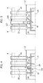
Figures 7 and 8 exemplify one or more embodiments applied to arrangements (such as QFP packages - QFP being an acronym for Quad Flat Package) including leads 10 facing a pad or slug 12 and defining agap 22 therewith without protruding above the pad orslug 12. - Here again, the
lead 10 and the pad or slug 12 may be regarded as extending in respective (at least approximately parallel) planes X10 and X12 (e.g. median planes of thelead 10 and the pad or slug 12, respectively) which are mutually offset with thecomponent 16 extending between these two planes. - In one or more embodiments as exemplified in
Figures 7 and 8 the electrically-conductive mass 20 discussed in the foregoing may be replaced by wire (or possibly ribbon) bonding 200 which electrically couples to thelead 10 the termination of thecomponent 16 opposite to the pad orslug 12. - Such wire or ribbon bonding of the
component 16 to thelead 10 may be: - direct, as exemplified in
Figure 7 , which may involve electrode finishing compatible with wire bonding technology, - indirect, as exemplified in
Figure 8 , that is via the die-pads 24a provided for the lead-to-diebonding 24 which may facilitate and optimized wire length. - One or more embodiments as exemplified in
Figures 7 and 8 may retain the advantage of arranging anelongate component 16 such as an EIA SIZE 0201 or EIA SIZE 0402 capacitor transverse to the pad or slug 12 (vertical, for instance) thus reducing the footprint of thecomponent 16 on the pad orslug 12. - One or more embodiments as exemplified in
Figures 7 and 8 are again exemplary of the possibility for thecomponent 16 to have a length longer than the distance between the lead 10 and the pad or slug 12, as measured transverse (orthogonal) to the planes X10 and X12, as a result of extending sidewise of thelead 10. - The diagram of
Figure 9 is exemplary of the impedance (Ohm) measured over a frequency range between 0.001 and 1.000 GHz for a 0201 SMD capacitor having a nominal capacitance value of 10 nF. - The impedance behavior for a capacitor assembly according to embodiments of the present description as (illustrated by the chained line in
Figure 9 ) shows an improvement in excess of 40% in comparison with the impedance behavior for a conventional capacitor assembly (shown in continuous line) over the whole of the frequency range above the frequency where the lowest impedance is measured. - One or more embodiments may thus provide an optimized electrical connection from a ground electrode (as provided by the pad or slug 12) to the back side of the die 14 achieved through a slug and not through a wire, while also exhibiting a shorter wire connection from the leads 10 (for instance a power lead) to the
die 14. - One or more embodiments may facilitate reducing (notionally halving) the number of dedicated power supply pins in a semiconductor device such as an integrated circuit in comparison with conventional planar SMD assembly, while also facilitating leadframe design standardization as discussed previously.
- A device as exemplified herein may comprise:
- at least one semiconductor chip (for instance, 14),
- a leadframe (for instance, 10, 12) comprising a chip mounting portion (for instance, 12) having the at least one semiconductor chip thereon and at least one lead (for instance, 10) arranged facing the chip mounting portion, the at least one lead lying in a first plane (for instance, X10) and the chip mounting portion lying in a second plane (for instance, X12), the first plane and the second plane mutually offset with a gap (for instance, 22) therebetween, and
- an electrical component (for instance, 16) arranged on the chip mounting portion and extending between the first plane and the second plane.
- A device as exemplified herein may comprise an elongate electrical component extending along a longitudinal axis (for instance, X16), the electrical component arranged on the chip mounting portion with said longitudinal axis transverse (for instance, orthogonal to) the second plane.
- A device as exemplified herein may comprise:
- a first electrically-conductive formation (for instance, 18) electrically coupling the chip mounting portion and the electrical component arranged on the chip mounting portion, and
- at least one second electrically-conductive formation (for instance, 20; 200; 200, 24) electrically coupling the electrical component to the at least one lead arranged facing the chip mounting portion.
- In a device as exemplified herein, the first electrically-conductive formation may comprise electrically-conductive material electrically and mechanically coupling the electrical component and the chip mounting portion.
- In a device as exemplified herein said at least one lead may be arranged facing and at least partially overlapping the chip mounting portion (see, for instance,
Figure 2 ), the electrical component extending bridge-like between the chip mounting portion and the at least one lead arranged facing the chip mounting portion. - In a device as exemplified herein the second electrically-conductive formation may comprise electrically-conductive material electrically and mechanically (see, for
instance 20 inFigure 2 ) coupling the electrical component to the at least one lead arranged facing and at least partially overlapping the chip mounting portion. - In a device as exemplified herein, the at least one second electrically-conductive formation may comprise wire-like (wire or ribbon) material (for instance, 200 or 200, 24) electrically coupling the electrical component to the at least one lead arranged facing the chip mounting portion either directly (see, for
instance 200 inFigure 7 ) or (see, forinstance Figure 8 ) via the at least one semiconductor chip on the chip mounting portion. - In a device as exemplified herein (see, for instance,
Figures 1 and 2 and Figures 3C to 3E ), the electrical component (for instance, 16) may extend sidewise of the at least one lead between the chip mounting portion and a lateral surface of the at least one lead in abutment with said lateral surface. - In a device as exemplified herein (see, for instance,
Figures 1 and 2 and Figures 3C to 3E plusFigures 7 and 8 ,) the electrical component may have a length longer than the distance between said chip mounting portion and said at least one lead transverse (orthogonal to, for instance) said first plane and said second plane. - A device as exemplified herein may comprise:
- at least one second lead (see, for instance, the
third lead 10 from left inFigure 5 ) in the leadframe arranged sidewise said at least one lead arranged facing the chip mounting portion, the at least one second lead mechanically and electrically coupled (100) to said at least one lead in the leadframe arranged facing the chip mounting portion, and - wire-like (for instance, wire of ribbon) bonding (see
Figure 5 ) between the at least one semiconductor chip on the chip mounting portion and the at least one second lead in the leadframe, wherein the electrical component is electrically coupled to the at least one semiconductor chip on the chip mounting portion via said wire-like bonding between the at least one semiconductor chip on the chip mounting portion and said at least one second lead in the leadframe. - A method of manufacturing a device as exemplified herein may comprise:
- arranging the at least one semiconductor chip on the chip mounting portion of the leadframe, the leadframe having said at least one lead arranged facing the chip mounting portion, the at least one lead lying in a first plane and the chip mounting portion lying in a second plane, the first plane and the second plane mutually offset with a gap therebetween,
- arranging the electrical component on the chip mounting portion (the electrical component) extending between the first plane and the second plane.
- A method as exemplified herein may comprise providing wire-like material (for instance, 24 in
Figures 4 and 5 ) electrically coupling the leadframe to the at least one semiconductor chip on the chip mounting portion, wherein providing said wire-like material may comprise applying clamping (for instance, at A) to the leadframe wherein the method may comprise refraining (for instance, at 102 inFigure 5 ) from applying clamping to said at the least one lead in the leadframe arranged facing the chip mounting portion. - Without prejudice to the underlying principles, the details and embodiments may vary, even significantly, with respect to what has been described by way of example only, without departing from the extent of protection. The extent of protection is determined by the annexed claims.
Claims (12)
- A device, comprising:- at least one semiconductor chip (14),- a leadframe (10, 12) comprising a chip mounting portion (12) having the at least one semiconductor chip (14) thereon and at least one lead (10) arranged facing the chip mounting portion (12), the at least one lead (10) lying in a first plane (X10) and the chip mounting portion (12) lying in a second plane (X12), the first plane (X10) and the second plane (X12) mutually offset with a gap (22) therebetween, and- an electrical component (16) arranged on the chip mounting portion (12) and extending between the first plane (X10) and the second plane (X12).
- The device of claim 1, comprising an elongate electrical component (16) extending along a longitudinal axis (X16), the electrical component (16) arranged on the chip mounting portion (12) with said longitudinal axis transverse the second plane (X12).
- The device of claim 1 or claim 2, comprising:- a first electrically-conductive formation (18) electrically coupling the chip mounting portion (12) and the electrical component (16) arranged on the chip mounting portion (12), and- at least one second electrically-conductive formation (20; 200; 200, 24) electrically coupling the electrical component (16) to the at least one lead (10) in the leadframe (10, 12) arranged facing the chip mounting portion (12).
- The device of claim 3, wherein the first electrically-conductive formation (18) comprises electrically-conductive material electrically and mechanically coupling the electrical component (16) and the chip mounting portion (12).
- The device of any of the previous claims, wherein said at least one lead (10) is arranged facing and at least partially overlapping the chip mounting portion (12), the electrical component (16) extending bridge-like between the chip mounting portion (12) and the at least one lead (10) arranged facing the chip mounting portion (12).
- The device of claim 4 and claim 5, wherein the second electrically-conductive formation (20) comprises electrically-conductive material electrically and mechanically coupling the electrical component (16) to the at least one lead (10) arranged facing and at least partially overlapping the chip mounting portion (12).
- The device of claim 3 or claim 4, wherein the at least one second electrically-conductive formation comprises wire-like material (200; 200, 24) electrically coupling the electrical component (16) to the at least one lead (10) arranged facing the chip mounting portion (12) either directly (200) or via (200, 24) the at least one semiconductor chip (14) on the chip mounting portion (12).
- The device of any of the previous claims, wherein the electrical component (16) extends sidewise of the at least one lead (10) between the chip mounting portion (12) and a lateral surface of the at least one lead (10) in abutment with said lateral surface.
- The device of any of the previous claims, wherein the electrical component (16) has a length longer than the distance between said chip mounting portion (12) and said at least one lead (10) transverse said first plane (X10) and said second plane (X12).
- The device of any of the previous claims, comprising:- at least one second lead (10) in the leadframe (10, 12) arranged sidewise said at least one lead (10) arranged facing the chip mounting portion (12), the at least one second lead (10) mechanically and electrically coupled (100) to said at least one lead (10) arranged facing the chip mounting portion (12), and- wire-like bonding (24) between the at least one semiconductor chip (14) on the chip mounting portion (12) and the at least one second lead (10) in the leadframe (10, 12), wherein the electrical component (16) is electrically coupled to the at least one semiconductor chip (14) on the chip mounting portion (12) via said wire-like bonding (24) between the at least one semiconductor chip (14) on the chip mounting portion (12) and said at least one second lead (10) in the leadframe (10, 12).
- A method of manufacturing a device according to any of claims 1 to 10, wherein the method comprises:- arranging the at least one semiconductor chip (14) on the chip mounting portion (12) of the leadframe (10, 12), the leadframe having said at least one lead (10) arranged facing the chip mounting portion (12), the at least one lead (10) lying in a first plane (X10) and the chip mounting portion (12) lying in a second plane (X12), the first plane (X10) and the second plane (X12) mutually offset with a gap (22) therebetween,- arranging the electrical component (16) on the chip mounting portion (12) extending between the first plane (X10) and the second plane (X12).
- The method of claim 11, comprising providing wire-like material (24) electrically coupling the leadframe (10, 12) to the at least one semiconductor chip (14) on the chip mounting portion (12), wherein providing said wire-like material (24) comprises applying clamping (A) to the leadframe (10, 12) wherein the method comprises refraining (102) from applying clamping to said at least one lead (10) in the leadframe (10, 12) arranged facing the chip mounting portion (12).
Applications Claiming Priority (1)
| Application Number | Priority Date | Filing Date | Title |
|---|---|---|---|
| IT102019000000929A IT201900000929A1 (en) | 2019-01-22 | 2019-01-22 | Semiconductor device and corresponding manufacturing process |
Publications (2)
| Publication Number | Publication Date |
|---|---|
| EP3686928A1 true EP3686928A1 (en) | 2020-07-29 |
| EP3686928B1 EP3686928B1 (en) | 2021-10-13 |
Family
ID=66049612
Family Applications (1)
| Application Number | Title | Priority Date | Filing Date |
|---|---|---|---|
| EP20151379.3A Active EP3686928B1 (en) | 2019-01-22 | 2020-01-13 | A semiconductor device and corresponding method of manufacture |
Country Status (4)
| Country | Link |
|---|---|
| US (2) | US11764134B2 (en) |
| EP (1) | EP3686928B1 (en) |
| CN (2) | CN111463183B (en) |
| IT (1) | IT201900000929A1 (en) |
Families Citing this family (2)
| Publication number | Priority date | Publication date | Assignee | Title |
|---|---|---|---|---|
| IT201900000929A1 (en) | 2019-01-22 | 2020-07-22 | St Microelectronics Srl | Semiconductor device and corresponding manufacturing process |
| CN113161319B (en) * | 2021-04-23 | 2022-03-22 | 长鑫存储技术有限公司 | Semiconductor structure and method of making the same |
Citations (8)
| Publication number | Priority date | Publication date | Assignee | Title |
|---|---|---|---|---|
| JPS61134060A (en) * | 1984-12-04 | 1986-06-21 | Nec Corp | Semiconductor device with built-in capacitor and manufacture thereof |
| JPS63132459A (en) * | 1986-11-25 | 1988-06-04 | Hitachi Ltd | Semiconductor package with built-in capacitor |
| JPH09199666A (en) * | 1996-01-23 | 1997-07-31 | Nec Eng Ltd | Semiconductor integrated circuit device |
| JPH1070234A (en) * | 1996-08-28 | 1998-03-10 | Nec Corp | IC package |
| US20020195693A1 (en) | 2001-06-22 | 2002-12-26 | Sheng-Tsung Liu | Packaging structure integrating passive devices |
| US6611434B1 (en) | 2000-10-30 | 2003-08-26 | Siliconware Precision Industries Co., Ltd. | Stacked multi-chip package structure with on-chip integration of passive component |
| US20080023843A1 (en) * | 2006-07-25 | 2008-01-31 | Noriaki Hiraga | Semiconductor device |
| US7960816B2 (en) | 2004-02-05 | 2011-06-14 | St Assembly Test Services Ltd. | Semiconductor package with passive device integration |
Family Cites Families (12)
| Publication number | Priority date | Publication date | Assignee | Title |
|---|---|---|---|---|
| JP2005302951A (en) * | 2004-04-09 | 2005-10-27 | Toshiba Corp | Power semiconductor device package |
| US20090020859A1 (en) * | 2007-07-18 | 2009-01-22 | Mediatek Inc. | Quad flat package with exposed common electrode bars |
| TWI364102B (en) * | 2007-12-20 | 2012-05-11 | Powertech Technology Inc | Semiconductor package with leads on a chip having muli-row bonding pads |
| DE102008054735A1 (en) * | 2008-12-16 | 2010-06-17 | Robert Bosch Gmbh | Leadless package housing |
| JP2010267728A (en) * | 2009-05-13 | 2010-11-25 | Renesas Electronics Corp | Semiconductor package, lead frame, and semiconductor package manufacturing method |
| CN204885153U (en) * | 2015-09-01 | 2015-12-16 | 苏州日月新半导体有限公司 | Integrated circuit packaging body |
| DE102017202770B4 (en) * | 2016-08-31 | 2023-06-07 | Infineon Technologies Austria Ag | Semiconductor die package having a repeating footprint pattern |
| US10468384B2 (en) | 2017-09-15 | 2019-11-05 | STATS ChipPAC Pte. Ltd. | Semiconductor device and method of forming embedded die substrate, and system-in-package modules with the same |
| US10818578B2 (en) | 2017-10-12 | 2020-10-27 | Stmicroelectronics S.R.L. | Method of manufacturing semiconductor devices, corresponding device and circuit |
| DE102018104972B4 (en) | 2018-03-05 | 2022-06-23 | Schweizer Electronic Ag | Printed circuit board element with an integrated electronic switching element, power converter and method for producing a printed circuit board element |
| IT201900000929A1 (en) | 2019-01-22 | 2020-07-22 | St Microelectronics Srl | Semiconductor device and corresponding manufacturing process |
| US12068276B2 (en) | 2019-01-22 | 2024-08-20 | Stmicroelectronics S.R.L. | Semiconductor device and corresponding method of manufacture |
-
2019
- 2019-01-22 IT IT102019000000929A patent/IT201900000929A1/en unknown
-
2020
- 2020-01-13 EP EP20151379.3A patent/EP3686928B1/en active Active
- 2020-01-16 US US16/745,043 patent/US11764134B2/en active Active
- 2020-01-22 CN CN202010075035.7A patent/CN111463183B/en active Active
- 2020-01-22 CN CN202020144512.6U patent/CN211376632U/en active Active
-
2023
- 2023-09-18 US US18/369,652 patent/US12300585B2/en active Active
Patent Citations (8)
| Publication number | Priority date | Publication date | Assignee | Title |
|---|---|---|---|---|
| JPS61134060A (en) * | 1984-12-04 | 1986-06-21 | Nec Corp | Semiconductor device with built-in capacitor and manufacture thereof |
| JPS63132459A (en) * | 1986-11-25 | 1988-06-04 | Hitachi Ltd | Semiconductor package with built-in capacitor |
| JPH09199666A (en) * | 1996-01-23 | 1997-07-31 | Nec Eng Ltd | Semiconductor integrated circuit device |
| JPH1070234A (en) * | 1996-08-28 | 1998-03-10 | Nec Corp | IC package |
| US6611434B1 (en) | 2000-10-30 | 2003-08-26 | Siliconware Precision Industries Co., Ltd. | Stacked multi-chip package structure with on-chip integration of passive component |
| US20020195693A1 (en) | 2001-06-22 | 2002-12-26 | Sheng-Tsung Liu | Packaging structure integrating passive devices |
| US7960816B2 (en) | 2004-02-05 | 2011-06-14 | St Assembly Test Services Ltd. | Semiconductor package with passive device integration |
| US20080023843A1 (en) * | 2006-07-25 | 2008-01-31 | Noriaki Hiraga | Semiconductor device |
Also Published As
| Publication number | Publication date |
|---|---|
| US20240006277A1 (en) | 2024-01-04 |
| IT201900000929A1 (en) | 2020-07-22 |
| CN111463183A (en) | 2020-07-28 |
| US11764134B2 (en) | 2023-09-19 |
| EP3686928B1 (en) | 2021-10-13 |
| US12300585B2 (en) | 2025-05-13 |
| US20200235045A1 (en) | 2020-07-23 |
| CN111463183B (en) | 2025-11-07 |
| CN211376632U (en) | 2020-08-28 |
Similar Documents
| Publication | Publication Date | Title |
|---|---|---|
| US12068276B2 (en) | Semiconductor device and corresponding method of manufacture | |
| DE102010038246B4 (en) | Surface mount, open cavity, wireless package for high power RF applications, method of manufacturing an RF semiconductor package and an RF semiconductor package assembly | |
| US6486535B2 (en) | Electronic package with surface-mountable device built therein | |
| US12300585B2 (en) | Semiconductor device with electrical component for bridging leadframe and chip mounting portion and corresponding method of manufacture | |
| US9779966B2 (en) | Lead frame and semiconductor device | |
| US9095067B2 (en) | Apparatus and method for vertically-structured passive components | |
| US11910519B2 (en) | Integrated circuit / printed circuit board assembly and method of manufacture | |
| US7443279B2 (en) | Coil package and bias tee package | |
| KR19990029974A (en) | Single leadframe package having a combined induction coil and an integrated circuit semiconductor chip, and a method of manufacturing the same | |
| DE112018007457B4 (en) | Semiconductor device | |
| CN101350318B (en) | Electronic package and electronic device | |
| US20210268598A1 (en) | Ribbon wire bond | |
| DE69421750T2 (en) | Potted plastic encapsulation for electronic arrangements | |
| US11854947B2 (en) | Integrated circuit chip with a vertical connector | |
| CN118263218A (en) | Dual down-set contact terminals for externally mounted passive components | |
| US7166905B1 (en) | Stacked paddle micro leadframe package | |
| CN205356806U (en) | LCC encapsulates pad | |
| KR930004255B1 (en) | Resin sealed semiconductor device | |
| US20240413120A1 (en) | Semiconductor device and corresponding method of manufacture | |
| JP4701779B2 (en) | Integrated circuit package assembly structure | |
| JP2001024139A (en) | Semiconductor device and method of manufacturing the same | |
| JPH06112395A (en) | Hybrid integrated circuit device | |
| US20100073893A1 (en) | Minimizing plating stub reflections in a chip package using capacitance | |
| CN116845035A (en) | Packaging structures and electronic devices | |
| JP2002057266A (en) | Electrical or opto-electrical components having plastic packaging and methods for changing the impedance of terminal leads of such components |
Legal Events
| Date | Code | Title | Description |
|---|---|---|---|
| PUAI | Public reference made under article 153(3) epc to a published international application that has entered the european phase |
Free format text: ORIGINAL CODE: 0009012 |
|
| STAA | Information on the status of an ep patent application or granted ep patent |
Free format text: STATUS: THE APPLICATION HAS BEEN PUBLISHED |
|
| AK | Designated contracting states |
Kind code of ref document: A1 Designated state(s): AL AT BE BG CH CY CZ DE DK EE ES FI FR GB GR HR HU IE IS IT LI LT LU LV MC MK MT NL NO PL PT RO RS SE SI SK SM TR |
|
| AX | Request for extension of the european patent |
Extension state: BA ME |
|
| STAA | Information on the status of an ep patent application or granted ep patent |
Free format text: STATUS: REQUEST FOR EXAMINATION WAS MADE |
|
| 17P | Request for examination filed |
Effective date: 20210128 |
|
| RBV | Designated contracting states (corrected) |
Designated state(s): AL AT BE BG CH CY CZ DE DK EE ES FI FR GB GR HR HU IE IS IT LI LT LU LV MC MK MT NL NO PL PT RO RS SE SI SK SM TR |
|
| GRAP | Despatch of communication of intention to grant a patent |
Free format text: ORIGINAL CODE: EPIDOSNIGR1 |
|
| STAA | Information on the status of an ep patent application or granted ep patent |
Free format text: STATUS: GRANT OF PATENT IS INTENDED |
|
| INTG | Intention to grant announced |
Effective date: 20210517 |
|
| GRAS | Grant fee paid |
Free format text: ORIGINAL CODE: EPIDOSNIGR3 |
|
| GRAA | (expected) grant |
Free format text: ORIGINAL CODE: 0009210 |
|
| STAA | Information on the status of an ep patent application or granted ep patent |
Free format text: STATUS: THE PATENT HAS BEEN GRANTED |
|
| AK | Designated contracting states |
Kind code of ref document: B1 Designated state(s): AL AT BE BG CH CY CZ DE DK EE ES FI FR GB GR HR HU IE IS IT LI LT LU LV MC MK MT NL NO PL PT RO RS SE SI SK SM TR |
|
| REG | Reference to a national code |
Ref country code: GB Ref legal event code: FG4D |
|
| REG | Reference to a national code |
Ref country code: CH Ref legal event code: EP |
|
| REG | Reference to a national code |
Ref country code: DE Ref legal event code: R096 Ref document number: 602020000693 Country of ref document: DE |
|
| REG | Reference to a national code |
Ref country code: IE Ref legal event code: FG4D |
|
| REG | Reference to a national code |
Ref country code: AT Ref legal event code: REF Ref document number: 1438805 Country of ref document: AT Kind code of ref document: T Effective date: 20211115 |
|
| REG | Reference to a national code |
Ref country code: LT Ref legal event code: MG9D |
|
| REG | Reference to a national code |
Ref country code: NL Ref legal event code: MP Effective date: 20211013 |
|
| REG | Reference to a national code |
Ref country code: AT Ref legal event code: MK05 Ref document number: 1438805 Country of ref document: AT Kind code of ref document: T Effective date: 20211013 |
|
| PG25 | Lapsed in a contracting state [announced via postgrant information from national office to epo] |
Ref country code: RS Free format text: LAPSE BECAUSE OF FAILURE TO SUBMIT A TRANSLATION OF THE DESCRIPTION OR TO PAY THE FEE WITHIN THE PRESCRIBED TIME-LIMIT Effective date: 20211013 Ref country code: LT Free format text: LAPSE BECAUSE OF FAILURE TO SUBMIT A TRANSLATION OF THE DESCRIPTION OR TO PAY THE FEE WITHIN THE PRESCRIBED TIME-LIMIT Effective date: 20211013 Ref country code: FI Free format text: LAPSE BECAUSE OF FAILURE TO SUBMIT A TRANSLATION OF THE DESCRIPTION OR TO PAY THE FEE WITHIN THE PRESCRIBED TIME-LIMIT Effective date: 20211013 Ref country code: BG Free format text: LAPSE BECAUSE OF FAILURE TO SUBMIT A TRANSLATION OF THE DESCRIPTION OR TO PAY THE FEE WITHIN THE PRESCRIBED TIME-LIMIT Effective date: 20220113 Ref country code: AT Free format text: LAPSE BECAUSE OF FAILURE TO SUBMIT A TRANSLATION OF THE DESCRIPTION OR TO PAY THE FEE WITHIN THE PRESCRIBED TIME-LIMIT Effective date: 20211013 |
|
| PG25 | Lapsed in a contracting state [announced via postgrant information from national office to epo] |
Ref country code: IS Free format text: LAPSE BECAUSE OF FAILURE TO SUBMIT A TRANSLATION OF THE DESCRIPTION OR TO PAY THE FEE WITHIN THE PRESCRIBED TIME-LIMIT Effective date: 20220213 Ref country code: SE Free format text: LAPSE BECAUSE OF FAILURE TO SUBMIT A TRANSLATION OF THE DESCRIPTION OR TO PAY THE FEE WITHIN THE PRESCRIBED TIME-LIMIT Effective date: 20211013 Ref country code: PT Free format text: LAPSE BECAUSE OF FAILURE TO SUBMIT A TRANSLATION OF THE DESCRIPTION OR TO PAY THE FEE WITHIN THE PRESCRIBED TIME-LIMIT Effective date: 20220214 Ref country code: PL Free format text: LAPSE BECAUSE OF FAILURE TO SUBMIT A TRANSLATION OF THE DESCRIPTION OR TO PAY THE FEE WITHIN THE PRESCRIBED TIME-LIMIT Effective date: 20211013 Ref country code: NO Free format text: LAPSE BECAUSE OF FAILURE TO SUBMIT A TRANSLATION OF THE DESCRIPTION OR TO PAY THE FEE WITHIN THE PRESCRIBED TIME-LIMIT Effective date: 20220113 Ref country code: NL Free format text: LAPSE BECAUSE OF FAILURE TO SUBMIT A TRANSLATION OF THE DESCRIPTION OR TO PAY THE FEE WITHIN THE PRESCRIBED TIME-LIMIT Effective date: 20211013 Ref country code: LV Free format text: LAPSE BECAUSE OF FAILURE TO SUBMIT A TRANSLATION OF THE DESCRIPTION OR TO PAY THE FEE WITHIN THE PRESCRIBED TIME-LIMIT Effective date: 20211013 Ref country code: HR Free format text: LAPSE BECAUSE OF FAILURE TO SUBMIT A TRANSLATION OF THE DESCRIPTION OR TO PAY THE FEE WITHIN THE PRESCRIBED TIME-LIMIT Effective date: 20211013 Ref country code: GR Free format text: LAPSE BECAUSE OF FAILURE TO SUBMIT A TRANSLATION OF THE DESCRIPTION OR TO PAY THE FEE WITHIN THE PRESCRIBED TIME-LIMIT Effective date: 20220114 Ref country code: ES Free format text: LAPSE BECAUSE OF FAILURE TO SUBMIT A TRANSLATION OF THE DESCRIPTION OR TO PAY THE FEE WITHIN THE PRESCRIBED TIME-LIMIT Effective date: 20211013 |
|
| REG | Reference to a national code |
Ref country code: DE Ref legal event code: R097 Ref document number: 602020000693 Country of ref document: DE |
|
| PG25 | Lapsed in a contracting state [announced via postgrant information from national office to epo] |
Ref country code: SM Free format text: LAPSE BECAUSE OF FAILURE TO SUBMIT A TRANSLATION OF THE DESCRIPTION OR TO PAY THE FEE WITHIN THE PRESCRIBED TIME-LIMIT Effective date: 20211013 Ref country code: SK Free format text: LAPSE BECAUSE OF FAILURE TO SUBMIT A TRANSLATION OF THE DESCRIPTION OR TO PAY THE FEE WITHIN THE PRESCRIBED TIME-LIMIT Effective date: 20211013 Ref country code: RO Free format text: LAPSE BECAUSE OF FAILURE TO SUBMIT A TRANSLATION OF THE DESCRIPTION OR TO PAY THE FEE WITHIN THE PRESCRIBED TIME-LIMIT Effective date: 20211013 Ref country code: EE Free format text: LAPSE BECAUSE OF FAILURE TO SUBMIT A TRANSLATION OF THE DESCRIPTION OR TO PAY THE FEE WITHIN THE PRESCRIBED TIME-LIMIT Effective date: 20211013 Ref country code: DK Free format text: LAPSE BECAUSE OF FAILURE TO SUBMIT A TRANSLATION OF THE DESCRIPTION OR TO PAY THE FEE WITHIN THE PRESCRIBED TIME-LIMIT Effective date: 20211013 Ref country code: CZ Free format text: LAPSE BECAUSE OF FAILURE TO SUBMIT A TRANSLATION OF THE DESCRIPTION OR TO PAY THE FEE WITHIN THE PRESCRIBED TIME-LIMIT Effective date: 20211013 |
|
| PLBE | No opposition filed within time limit |
Free format text: ORIGINAL CODE: 0009261 |
|
| STAA | Information on the status of an ep patent application or granted ep patent |
Free format text: STATUS: NO OPPOSITION FILED WITHIN TIME LIMIT |
|
| PG25 | Lapsed in a contracting state [announced via postgrant information from national office to epo] |
Ref country code: MC Free format text: LAPSE BECAUSE OF FAILURE TO SUBMIT A TRANSLATION OF THE DESCRIPTION OR TO PAY THE FEE WITHIN THE PRESCRIBED TIME-LIMIT Effective date: 20211013 |
|
| 26N | No opposition filed |
Effective date: 20220714 |
|
| REG | Reference to a national code |
Ref country code: BE Ref legal event code: MM Effective date: 20220131 |
|
| PG25 | Lapsed in a contracting state [announced via postgrant information from national office to epo] |
Ref country code: LU Free format text: LAPSE BECAUSE OF NON-PAYMENT OF DUE FEES Effective date: 20220113 Ref country code: AL Free format text: LAPSE BECAUSE OF FAILURE TO SUBMIT A TRANSLATION OF THE DESCRIPTION OR TO PAY THE FEE WITHIN THE PRESCRIBED TIME-LIMIT Effective date: 20211013 |
|
| PG25 | Lapsed in a contracting state [announced via postgrant information from national office to epo] |
Ref country code: SI Free format text: LAPSE BECAUSE OF FAILURE TO SUBMIT A TRANSLATION OF THE DESCRIPTION OR TO PAY THE FEE WITHIN THE PRESCRIBED TIME-LIMIT Effective date: 20211013 Ref country code: FR Free format text: LAPSE BECAUSE OF NON-PAYMENT OF DUE FEES Effective date: 20220131 Ref country code: BE Free format text: LAPSE BECAUSE OF NON-PAYMENT OF DUE FEES Effective date: 20220131 |
|
| PG25 | Lapsed in a contracting state [announced via postgrant information from national office to epo] |
Ref country code: IE Free format text: LAPSE BECAUSE OF NON-PAYMENT OF DUE FEES Effective date: 20220113 |
|
| PG25 | Lapsed in a contracting state [announced via postgrant information from national office to epo] |
Ref country code: IT Free format text: LAPSE BECAUSE OF FAILURE TO SUBMIT A TRANSLATION OF THE DESCRIPTION OR TO PAY THE FEE WITHIN THE PRESCRIBED TIME-LIMIT Effective date: 20211013 |
|
| REG | Reference to a national code |
Ref country code: CH Ref legal event code: PL |
|
| PG25 | Lapsed in a contracting state [announced via postgrant information from national office to epo] |
Ref country code: LI Free format text: LAPSE BECAUSE OF NON-PAYMENT OF DUE FEES Effective date: 20230131 Ref country code: CH Free format text: LAPSE BECAUSE OF NON-PAYMENT OF DUE FEES Effective date: 20230131 |
|
| PG25 | Lapsed in a contracting state [announced via postgrant information from national office to epo] |
Ref country code: MK Free format text: LAPSE BECAUSE OF FAILURE TO SUBMIT A TRANSLATION OF THE DESCRIPTION OR TO PAY THE FEE WITHIN THE PRESCRIBED TIME-LIMIT Effective date: 20211013 Ref country code: CY Free format text: LAPSE BECAUSE OF FAILURE TO SUBMIT A TRANSLATION OF THE DESCRIPTION OR TO PAY THE FEE WITHIN THE PRESCRIBED TIME-LIMIT Effective date: 20211013 |
|
| PG25 | Lapsed in a contracting state [announced via postgrant information from national office to epo] |
Ref country code: HU Free format text: LAPSE BECAUSE OF FAILURE TO SUBMIT A TRANSLATION OF THE DESCRIPTION OR TO PAY THE FEE WITHIN THE PRESCRIBED TIME-LIMIT; INVALID AB INITIO Effective date: 20200113 |
|
| GBPC | Gb: european patent ceased through non-payment of renewal fee |
Effective date: 20240113 |
|
| PG25 | Lapsed in a contracting state [announced via postgrant information from national office to epo] |
Ref country code: MT Free format text: LAPSE BECAUSE OF FAILURE TO SUBMIT A TRANSLATION OF THE DESCRIPTION OR TO PAY THE FEE WITHIN THE PRESCRIBED TIME-LIMIT Effective date: 20211013 |
|
| PG25 | Lapsed in a contracting state [announced via postgrant information from national office to epo] |
Ref country code: GB Free format text: LAPSE BECAUSE OF NON-PAYMENT OF DUE FEES Effective date: 20240113 |
|
| PG25 | Lapsed in a contracting state [announced via postgrant information from national office to epo] |
Ref country code: GB Free format text: LAPSE BECAUSE OF NON-PAYMENT OF DUE FEES Effective date: 20240113 |
|
| PGFP | Annual fee paid to national office [announced via postgrant information from national office to epo] |
Ref country code: DE Payment date: 20241218 Year of fee payment: 6 |
|
| REG | Reference to a national code |
Ref country code: DE Ref legal event code: R079 Ref document number: 602020000693 Country of ref document: DE Free format text: PREVIOUS MAIN CLASS: H01L0023495000 Ipc: H10W0070400000 |
|
| PG25 | Lapsed in a contracting state [announced via postgrant information from national office to epo] |
Ref country code: TR Free format text: LAPSE BECAUSE OF FAILURE TO SUBMIT A TRANSLATION OF THE DESCRIPTION OR TO PAY THE FEE WITHIN THE PRESCRIBED TIME-LIMIT Effective date: 20211013 |