EP3686715B1 - Anzeigevorrichtung mit adhäsionsverringerungsschicht mit mikrovorsprungmuster - Google Patents
Anzeigevorrichtung mit adhäsionsverringerungsschicht mit mikrovorsprungmuster Download PDFInfo
- Publication number
- EP3686715B1 EP3686715B1 EP18858672.1A EP18858672A EP3686715B1 EP 3686715 B1 EP3686715 B1 EP 3686715B1 EP 18858672 A EP18858672 A EP 18858672A EP 3686715 B1 EP3686715 B1 EP 3686715B1
- Authority
- EP
- European Patent Office
- Prior art keywords
- layer
- adhesion reduction
- window
- display device
- reduction layer
- Prior art date
- Legal status (The legal status is an assumption and is not a legal conclusion. Google has not performed a legal analysis and makes no representation as to the accuracy of the status listed.)
- Active
Links
Images




Classifications
-
- G—PHYSICS
- G02—OPTICS
- G02F—OPTICAL DEVICES OR ARRANGEMENTS FOR THE CONTROL OF LIGHT BY MODIFICATION OF THE OPTICAL PROPERTIES OF THE MEDIA OF THE ELEMENTS INVOLVED THEREIN; NON-LINEAR OPTICS; FREQUENCY-CHANGING OF LIGHT; OPTICAL LOGIC ELEMENTS; OPTICAL ANALOGUE/DIGITAL CONVERTERS
- G02F1/00—Devices or arrangements for the control of the intensity, colour, phase, polarisation or direction of light arriving from an independent light source, e.g. switching, gating or modulating; Non-linear optics
- G02F1/01—Devices or arrangements for the control of the intensity, colour, phase, polarisation or direction of light arriving from an independent light source, e.g. switching, gating or modulating; Non-linear optics for the control of the intensity, phase, polarisation or colour
- G02F1/13—Devices or arrangements for the control of the intensity, colour, phase, polarisation or direction of light arriving from an independent light source, e.g. switching, gating or modulating; Non-linear optics for the control of the intensity, phase, polarisation or colour based on liquid crystals, e.g. single liquid crystal display cells
- G02F1/133—Constructional arrangements; Operation of liquid crystal cells; Circuit arrangements
- G02F1/1333—Constructional arrangements; Manufacturing methods
- G02F1/133308—Support structures for LCD panels, e.g. frames or bezels
-
- G—PHYSICS
- G06—COMPUTING OR CALCULATING; COUNTING
- G06F—ELECTRIC DIGITAL DATA PROCESSING
- G06F3/00—Input arrangements for transferring data to be processed into a form capable of being handled by the computer; Output arrangements for transferring data from processing unit to output unit, e.g. interface arrangements
- G06F3/01—Input arrangements or combined input and output arrangements for interaction between user and computer
- G06F3/03—Arrangements for converting the position or the displacement of a member into a coded form
- G06F3/041—Digitisers, e.g. for touch screens or touch pads, characterised by the transducing means
- G06F3/0412—Digitisers structurally integrated in a display
-
- B—PERFORMING OPERATIONS; TRANSPORTING
- B32—LAYERED PRODUCTS
- B32B—LAYERED PRODUCTS, i.e. PRODUCTS BUILT-UP OF STRATA OF FLAT OR NON-FLAT, e.g. CELLULAR OR HONEYCOMB, FORM
- B32B27/00—Layered products comprising a layer of synthetic resin
- B32B27/06—Layered products comprising a layer of synthetic resin as the main or only constituent of a layer, which is next to another layer of the same or of a different material
- B32B27/08—Layered products comprising a layer of synthetic resin as the main or only constituent of a layer, which is next to another layer of the same or of a different material of synthetic resin
-
- B—PERFORMING OPERATIONS; TRANSPORTING
- B32—LAYERED PRODUCTS
- B32B—LAYERED PRODUCTS, i.e. PRODUCTS BUILT-UP OF STRATA OF FLAT OR NON-FLAT, e.g. CELLULAR OR HONEYCOMB, FORM
- B32B27/00—Layered products comprising a layer of synthetic resin
- B32B27/28—Layered products comprising a layer of synthetic resin comprising synthetic resins not wholly covered by any one of the sub-groups B32B27/30 - B32B27/42
- B32B27/281—Layered products comprising a layer of synthetic resin comprising synthetic resins not wholly covered by any one of the sub-groups B32B27/30 - B32B27/42 comprising polyimides
-
- B—PERFORMING OPERATIONS; TRANSPORTING
- B32—LAYERED PRODUCTS
- B32B—LAYERED PRODUCTS, i.e. PRODUCTS BUILT-UP OF STRATA OF FLAT OR NON-FLAT, e.g. CELLULAR OR HONEYCOMB, FORM
- B32B27/00—Layered products comprising a layer of synthetic resin
- B32B27/28—Layered products comprising a layer of synthetic resin comprising synthetic resins not wholly covered by any one of the sub-groups B32B27/30 - B32B27/42
- B32B27/283—Layered products comprising a layer of synthetic resin comprising synthetic resins not wholly covered by any one of the sub-groups B32B27/30 - B32B27/42 comprising polysiloxanes
-
- B—PERFORMING OPERATIONS; TRANSPORTING
- B32—LAYERED PRODUCTS
- B32B—LAYERED PRODUCTS, i.e. PRODUCTS BUILT-UP OF STRATA OF FLAT OR NON-FLAT, e.g. CELLULAR OR HONEYCOMB, FORM
- B32B27/00—Layered products comprising a layer of synthetic resin
- B32B27/28—Layered products comprising a layer of synthetic resin comprising synthetic resins not wholly covered by any one of the sub-groups B32B27/30 - B32B27/42
- B32B27/286—Layered products comprising a layer of synthetic resin comprising synthetic resins not wholly covered by any one of the sub-groups B32B27/30 - B32B27/42 comprising polysulphones; polysulfides
-
- B—PERFORMING OPERATIONS; TRANSPORTING
- B32—LAYERED PRODUCTS
- B32B—LAYERED PRODUCTS, i.e. PRODUCTS BUILT-UP OF STRATA OF FLAT OR NON-FLAT, e.g. CELLULAR OR HONEYCOMB, FORM
- B32B27/00—Layered products comprising a layer of synthetic resin
- B32B27/30—Layered products comprising a layer of synthetic resin comprising vinyl (co)polymers; comprising acrylic (co)polymers
- B32B27/308—Layered products comprising a layer of synthetic resin comprising vinyl (co)polymers; comprising acrylic (co)polymers comprising acrylic (co)polymers
-
- B—PERFORMING OPERATIONS; TRANSPORTING
- B32—LAYERED PRODUCTS
- B32B—LAYERED PRODUCTS, i.e. PRODUCTS BUILT-UP OF STRATA OF FLAT OR NON-FLAT, e.g. CELLULAR OR HONEYCOMB, FORM
- B32B27/00—Layered products comprising a layer of synthetic resin
- B32B27/32—Layered products comprising a layer of synthetic resin comprising polyolefins
- B32B27/325—Layered products comprising a layer of synthetic resin comprising polyolefins comprising polycycloolefins
-
- B—PERFORMING OPERATIONS; TRANSPORTING
- B32—LAYERED PRODUCTS
- B32B—LAYERED PRODUCTS, i.e. PRODUCTS BUILT-UP OF STRATA OF FLAT OR NON-FLAT, e.g. CELLULAR OR HONEYCOMB, FORM
- B32B27/00—Layered products comprising a layer of synthetic resin
- B32B27/36—Layered products comprising a layer of synthetic resin comprising polyesters
-
- B—PERFORMING OPERATIONS; TRANSPORTING
- B32—LAYERED PRODUCTS
- B32B—LAYERED PRODUCTS, i.e. PRODUCTS BUILT-UP OF STRATA OF FLAT OR NON-FLAT, e.g. CELLULAR OR HONEYCOMB, FORM
- B32B27/00—Layered products comprising a layer of synthetic resin
- B32B27/36—Layered products comprising a layer of synthetic resin comprising polyesters
- B32B27/365—Layered products comprising a layer of synthetic resin comprising polyesters comprising polycarbonates
-
- B—PERFORMING OPERATIONS; TRANSPORTING
- B32—LAYERED PRODUCTS
- B32B—LAYERED PRODUCTS, i.e. PRODUCTS BUILT-UP OF STRATA OF FLAT OR NON-FLAT, e.g. CELLULAR OR HONEYCOMB, FORM
- B32B3/00—Layered products comprising a layer with external or internal discontinuities or unevennesses, or a layer of non-planar shape; Layered products comprising a layer having particular features of form
- B32B3/02—Layered products comprising a layer with external or internal discontinuities or unevennesses, or a layer of non-planar shape; Layered products comprising a layer having particular features of form characterised by features of form at particular places, e.g. in edge regions
- B32B3/06—Layered products comprising a layer with external or internal discontinuities or unevennesses, or a layer of non-planar shape; Layered products comprising a layer having particular features of form characterised by features of form at particular places, e.g. in edge regions for securing layers together; for attaching the product to another member, e.g. to a support, or to another product, e.g. groove/tongue, interlocking
-
- B—PERFORMING OPERATIONS; TRANSPORTING
- B32—LAYERED PRODUCTS
- B32B—LAYERED PRODUCTS, i.e. PRODUCTS BUILT-UP OF STRATA OF FLAT OR NON-FLAT, e.g. CELLULAR OR HONEYCOMB, FORM
- B32B3/00—Layered products comprising a layer with external or internal discontinuities or unevennesses, or a layer of non-planar shape; Layered products comprising a layer having particular features of form
- B32B3/26—Layered products comprising a layer with external or internal discontinuities or unevennesses, or a layer of non-planar shape; Layered products comprising a layer having particular features of form characterised by a particular shape of the outline of the cross-section of a continuous layer; characterised by a layer with cavities or internal voids ; characterised by an apertured layer
- B32B3/30—Layered products comprising a layer with external or internal discontinuities or unevennesses, or a layer of non-planar shape; Layered products comprising a layer having particular features of form characterised by a particular shape of the outline of the cross-section of a continuous layer; characterised by a layer with cavities or internal voids ; characterised by an apertured layer characterised by a layer formed with recesses or projections, e.g. hollows, grooves, protuberances, ribs
-
- B—PERFORMING OPERATIONS; TRANSPORTING
- B32—LAYERED PRODUCTS
- B32B—LAYERED PRODUCTS, i.e. PRODUCTS BUILT-UP OF STRATA OF FLAT OR NON-FLAT, e.g. CELLULAR OR HONEYCOMB, FORM
- B32B7/00—Layered products characterised by the relation between layers; Layered products characterised by the relative orientation of features between layers, or by the relative values of a measurable parameter between layers, i.e. products comprising layers having different physical, chemical or physicochemical properties; Layered products characterised by the interconnection of layers
- B32B7/04—Interconnection of layers
- B32B7/06—Interconnection of layers permitting easy separation
-
- B—PERFORMING OPERATIONS; TRANSPORTING
- B32—LAYERED PRODUCTS
- B32B—LAYERED PRODUCTS, i.e. PRODUCTS BUILT-UP OF STRATA OF FLAT OR NON-FLAT, e.g. CELLULAR OR HONEYCOMB, FORM
- B32B7/00—Layered products characterised by the relation between layers; Layered products characterised by the relative orientation of features between layers, or by the relative values of a measurable parameter between layers, i.e. products comprising layers having different physical, chemical or physicochemical properties; Layered products characterised by the interconnection of layers
- B32B7/04—Interconnection of layers
- B32B7/12—Interconnection of layers using interposed adhesives or interposed materials with bonding properties
-
- C—CHEMISTRY; METALLURGY
- C08—ORGANIC MACROMOLECULAR COMPOUNDS; THEIR PREPARATION OR CHEMICAL WORKING-UP; COMPOSITIONS BASED THEREON
- C08G—MACROMOLECULAR COMPOUNDS OBTAINED OTHERWISE THAN BY REACTIONS ONLY INVOLVING UNSATURATED CARBON-TO-CARBON BONDS
- C08G18/00—Polymeric products of isocyanates or isothiocyanates
- C08G18/06—Polymeric products of isocyanates or isothiocyanates with compounds having active hydrogen
- C08G18/28—Polymeric products of isocyanates or isothiocyanates with compounds having active hydrogen characterised by the compounds used containing active hydrogen
- C08G18/30—Low-molecular-weight compounds
- C08G18/38—Low-molecular-weight compounds having heteroatoms other than oxygen
- C08G18/3802—Low-molecular-weight compounds having heteroatoms other than oxygen having halogens
- C08G18/3804—Polyhydroxy compounds
- C08G18/3812—Polyhydroxy compounds having fluorine atoms
-
- C—CHEMISTRY; METALLURGY
- C08—ORGANIC MACROMOLECULAR COMPOUNDS; THEIR PREPARATION OR CHEMICAL WORKING-UP; COMPOSITIONS BASED THEREON
- C08G—MACROMOLECULAR COMPOUNDS OBTAINED OTHERWISE THAN BY REACTIONS ONLY INVOLVING UNSATURATED CARBON-TO-CARBON BONDS
- C08G18/00—Polymeric products of isocyanates or isothiocyanates
- C08G18/06—Polymeric products of isocyanates or isothiocyanates with compounds having active hydrogen
- C08G18/28—Polymeric products of isocyanates or isothiocyanates with compounds having active hydrogen characterised by the compounds used containing active hydrogen
- C08G18/40—High-molecular-weight compounds
- C08G18/58—Epoxy resins
- C08G18/588—Epoxy resins having silicon
-
- G—PHYSICS
- G06—COMPUTING OR CALCULATING; COUNTING
- G06F—ELECTRIC DIGITAL DATA PROCESSING
- G06F3/00—Input arrangements for transferring data to be processed into a form capable of being handled by the computer; Output arrangements for transferring data from processing unit to output unit, e.g. interface arrangements
- G06F3/01—Input arrangements or combined input and output arrangements for interaction between user and computer
- G06F3/03—Arrangements for converting the position or the displacement of a member into a coded form
- G06F3/041—Digitisers, e.g. for touch screens or touch pads, characterised by the transducing means
-
- B—PERFORMING OPERATIONS; TRANSPORTING
- B32—LAYERED PRODUCTS
- B32B—LAYERED PRODUCTS, i.e. PRODUCTS BUILT-UP OF STRATA OF FLAT OR NON-FLAT, e.g. CELLULAR OR HONEYCOMB, FORM
- B32B2255/00—Coating on the layer surface
- B32B2255/10—Coating on the layer surface on synthetic resin layer or on natural or synthetic rubber layer
-
- B—PERFORMING OPERATIONS; TRANSPORTING
- B32—LAYERED PRODUCTS
- B32B—LAYERED PRODUCTS, i.e. PRODUCTS BUILT-UP OF STRATA OF FLAT OR NON-FLAT, e.g. CELLULAR OR HONEYCOMB, FORM
- B32B2255/00—Coating on the layer surface
- B32B2255/20—Inorganic coating
-
- B—PERFORMING OPERATIONS; TRANSPORTING
- B32—LAYERED PRODUCTS
- B32B—LAYERED PRODUCTS, i.e. PRODUCTS BUILT-UP OF STRATA OF FLAT OR NON-FLAT, e.g. CELLULAR OR HONEYCOMB, FORM
- B32B2255/00—Coating on the layer surface
- B32B2255/28—Multiple coating on one surface
-
- B—PERFORMING OPERATIONS; TRANSPORTING
- B32—LAYERED PRODUCTS
- B32B—LAYERED PRODUCTS, i.e. PRODUCTS BUILT-UP OF STRATA OF FLAT OR NON-FLAT, e.g. CELLULAR OR HONEYCOMB, FORM
- B32B2307/00—Properties of the layers or laminate
- B32B2307/40—Properties of the layers or laminate having particular optical properties
- B32B2307/412—Transparent
-
- B—PERFORMING OPERATIONS; TRANSPORTING
- B32—LAYERED PRODUCTS
- B32B—LAYERED PRODUCTS, i.e. PRODUCTS BUILT-UP OF STRATA OF FLAT OR NON-FLAT, e.g. CELLULAR OR HONEYCOMB, FORM
- B32B2307/00—Properties of the layers or laminate
- B32B2307/50—Properties of the layers or laminate having particular mechanical properties
- B32B2307/538—Roughness
-
- B—PERFORMING OPERATIONS; TRANSPORTING
- B32—LAYERED PRODUCTS
- B32B—LAYERED PRODUCTS, i.e. PRODUCTS BUILT-UP OF STRATA OF FLAT OR NON-FLAT, e.g. CELLULAR OR HONEYCOMB, FORM
- B32B2307/00—Properties of the layers or laminate
- B32B2307/70—Other properties
- B32B2307/748—Releasability
-
- B—PERFORMING OPERATIONS; TRANSPORTING
- B32—LAYERED PRODUCTS
- B32B—LAYERED PRODUCTS, i.e. PRODUCTS BUILT-UP OF STRATA OF FLAT OR NON-FLAT, e.g. CELLULAR OR HONEYCOMB, FORM
- B32B2307/00—Properties of the layers or laminate
- B32B2307/70—Other properties
- B32B2307/75—Printability
-
- B—PERFORMING OPERATIONS; TRANSPORTING
- B32—LAYERED PRODUCTS
- B32B—LAYERED PRODUCTS, i.e. PRODUCTS BUILT-UP OF STRATA OF FLAT OR NON-FLAT, e.g. CELLULAR OR HONEYCOMB, FORM
- B32B2405/00—Adhesive articles, e.g. adhesive tapes
-
- B—PERFORMING OPERATIONS; TRANSPORTING
- B32—LAYERED PRODUCTS
- B32B—LAYERED PRODUCTS, i.e. PRODUCTS BUILT-UP OF STRATA OF FLAT OR NON-FLAT, e.g. CELLULAR OR HONEYCOMB, FORM
- B32B2457/00—Electrical equipment
- B32B2457/20—Displays, e.g. liquid crystal displays, plasma displays
-
- B—PERFORMING OPERATIONS; TRANSPORTING
- B32—LAYERED PRODUCTS
- B32B—LAYERED PRODUCTS, i.e. PRODUCTS BUILT-UP OF STRATA OF FLAT OR NON-FLAT, e.g. CELLULAR OR HONEYCOMB, FORM
- B32B2457/00—Electrical equipment
- B32B2457/20—Displays, e.g. liquid crystal displays, plasma displays
- B32B2457/202—LCD, i.e. liquid crystal displays
-
- B—PERFORMING OPERATIONS; TRANSPORTING
- B32—LAYERED PRODUCTS
- B32B—LAYERED PRODUCTS, i.e. PRODUCTS BUILT-UP OF STRATA OF FLAT OR NON-FLAT, e.g. CELLULAR OR HONEYCOMB, FORM
- B32B2457/00—Electrical equipment
- B32B2457/20—Displays, e.g. liquid crystal displays, plasma displays
- B32B2457/206—Organic displays, e.g. OLED
-
- B—PERFORMING OPERATIONS; TRANSPORTING
- B32—LAYERED PRODUCTS
- B32B—LAYERED PRODUCTS, i.e. PRODUCTS BUILT-UP OF STRATA OF FLAT OR NON-FLAT, e.g. CELLULAR OR HONEYCOMB, FORM
- B32B2457/00—Electrical equipment
- B32B2457/20—Displays, e.g. liquid crystal displays, plasma displays
- B32B2457/208—Touch screens
-
- G—PHYSICS
- G02—OPTICS
- G02F—OPTICAL DEVICES OR ARRANGEMENTS FOR THE CONTROL OF LIGHT BY MODIFICATION OF THE OPTICAL PROPERTIES OF THE MEDIA OF THE ELEMENTS INVOLVED THEREIN; NON-LINEAR OPTICS; FREQUENCY-CHANGING OF LIGHT; OPTICAL LOGIC ELEMENTS; OPTICAL ANALOGUE/DIGITAL CONVERTERS
- G02F1/00—Devices or arrangements for the control of the intensity, colour, phase, polarisation or direction of light arriving from an independent light source, e.g. switching, gating or modulating; Non-linear optics
- G02F1/01—Devices or arrangements for the control of the intensity, colour, phase, polarisation or direction of light arriving from an independent light source, e.g. switching, gating or modulating; Non-linear optics for the control of the intensity, phase, polarisation or colour
- G02F1/13—Devices or arrangements for the control of the intensity, colour, phase, polarisation or direction of light arriving from an independent light source, e.g. switching, gating or modulating; Non-linear optics for the control of the intensity, phase, polarisation or colour based on liquid crystals, e.g. single liquid crystal display cells
- G02F1/133—Constructional arrangements; Operation of liquid crystal cells; Circuit arrangements
- G02F1/1333—Constructional arrangements; Manufacturing methods
- G02F1/133308—Support structures for LCD panels, e.g. frames or bezels
- G02F1/133331—Cover glasses
-
- G—PHYSICS
- G02—OPTICS
- G02F—OPTICAL DEVICES OR ARRANGEMENTS FOR THE CONTROL OF LIGHT BY MODIFICATION OF THE OPTICAL PROPERTIES OF THE MEDIA OF THE ELEMENTS INVOLVED THEREIN; NON-LINEAR OPTICS; FREQUENCY-CHANGING OF LIGHT; OPTICAL LOGIC ELEMENTS; OPTICAL ANALOGUE/DIGITAL CONVERTERS
- G02F2202/00—Materials and properties
- G02F2202/28—Adhesive materials or arrangements
-
- G—PHYSICS
- G06—COMPUTING OR CALCULATING; COUNTING
- G06F—ELECTRIC DIGITAL DATA PROCESSING
- G06F2203/00—Indexing scheme relating to G06F3/00 - G06F3/048
- G06F2203/041—Indexing scheme relating to G06F3/041 - G06F3/045
- G06F2203/04103—Manufacturing, i.e. details related to manufacturing processes specially suited for touch sensitive devices
Definitions
- the present invention relates to a display device, and more specifically, to a display device applying a window or a touch screen that can be attached and detached using an adhesion reduction layer having a pattern configured of micro protrusions.
- a display such as a liquid crystal display (LCD), an organic light emitting diode (OLED), or an electrophoretic display (EPD) forms a screen.
- LCD liquid crystal display
- OLED organic light emitting diode
- EPD electrophoretic display
- a touch screen to provide convenience of handling.
- a window made of tempered glass or transparent polymer resin is disposed on the front surface of the touch screen.
- the window is divided into a screen unit at the center and a bezel unit on the rim, and protects the display device from damage caused by external impact or contact.
- the window is bonded and fixed to the touch screen using an optically clear adhesive (OCA), ultraviolet curable adhesive or the like.
- OCA optically clear adhesive
- Korean Patent Registration No. 10-1574923 proposes a display device including a detachable window and an attaching and detaching method thereof.
- the patent may easily replace a damaged window, easily separate the window from the display device, simplify the process of manufacturing the display device, reduce manufacturing cost, and design display device in various ways.
- a display device capable of attaching and detaching a touch screen is also possible.
- the display device may be manufactured by obtaining and assembling a window, a touch screen and a display through different channels, such as different manufacturers or products.
- product A of company A, product B of company B, and product C of company C may be obtained as the window, the touch screen and the display through different purchase channels respectively and assembled as a display device including A, B and C.
- authenticity of the display device according to the patent may not be confirmed since it is difficult to confirm the different channels.
- products of different channels may have their own patterns for identification of the products or for enhancement of aesthetics, the patterns may not be known before assembling the products.
- WO 2016/117820 A1 discloses a display device comprising a window structure in which an attachment/detachment layer having adhesive strength of 0.1 gf/25mm to 500 gf/25mm is formed on the entire surface of one side of a window.
- WO 2016/120710 A1 (FUJIMORI KOGYO CO ) provides an adhesive resin layer, which can prevent generation of air bubbles even when adhered to a substrate having a high level.
- US 2015/060870 A1 (RO JAE-SANG ) a supporting substrate for manufacturing a flexible information display device capable of easily separating the flexible information display device from the supporting substrate without deforming or damaging the flexible information display device.
- JP 2014 224919 A (NEC CORP ) a display device that has high repairability and visibility.
- the present invention has been made in view of the above problems, and it is an object of the present invention to provide a display device including an adhesion reduction layer having a micro protrusion pattern, which can confirm the authenticity and engraved pattern of at least one product among a window, a touch screen and a display that are freely attached and detached, and obtained through different channels.
- a display device including an adhesion reduction layer having a micro protrusion pattern of the present invention, as a pattern configured of micro protrusions is formed on the adhesion reduction layer, the authenticity and engraved pattern of at least one product among a window, a touch screen and a display that are freely attached and detached, and obtained through different channels can be confirmed.
- Display 14 Touch screen 16: Adhesion reduction layer 16a: Pattern 18: Detachable layer 20: Window
- the present invention proposes a display device, which can confirm the authenticity and engraved pattern of at least one product among a window, a touch screen and a display that are freely attached and detached, and obtained through different channels, by forming a pattern configured of micro protrusions on the adhesion reduction layer.
- the window structure or the touch screen of the display device has a detachable layer formed to be attached to and detached from the touch screen or the display.
- a being-adhered device to be attached and detached may be regarded as being associated with the touch screen or the display.
- attachment and detachment means freely attaching and detaching the detachable layer to and from the being-adhered device.
- the detachable layer of the present invention is attached and detached only to and from the touch screen and the display, and is clearly distinguished from a conventional window protection film attached to and detached from the window. That is, a device configured of a display without a window or a touch screen of the present invention is not a display device of a completed form. The display device is completed only when the window or the touch screen of the present invention is attached.
- a window protection film is attached on the window of the present invention, and the window protection film is attached to an already completed display. Accordingly, the window or the touch screen of the present invention is an essential component constituting the display device, whereas a conventional window protection film corresponds to an auxiliary component that can be selectively applied to a display device. Accordingly, the window protection film is excluded from the scope of the present invention.
- the conventional window protection film is not part of the present invention.
- the display device applied to the present invention refers to image processing devices such as a mobile device, an information processing terminal, a television, and the like.
- the mobile device may be a cellular phone, a smartphone, a tablet or the like, and the information processing terminal may be an ATM, a kiosk or the like.
- the display of the display device may be a flat or curved one, or may be a flexible one.
- the image processing device includes a window, a touch screen and a display. Accordingly, the window generally refers to a window of a mobile devices, a windows of an information processing terminal, and windows of all image processing devices such as a television and the like. Similarly, the touch screen and the display also refer to touch screens and displays applied to all image processing devices.
- the window structure is divided into first to fifth window structures attached to and detached from the touch screen and the display for convenience of explanation. That is, the first to fifth window structures are attached to and detached from the touch screen, the cover layer of the touch screen, and the display (hereinafter, referred to as an being-adhered device).
- the first to fifth window structures will be separately described.
- a detachable layer is on a window or a touch screen
- an adhesion reduction layer is on a corresponding touch screen or display.
- an adhesion reduction layer is on a window or a touch screen
- a detachable layer may be on a corresponding touch screen or display.
- the prior case will be described as an example. Display devices without an adhesion reduction layer are not within the scope of the claims.
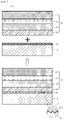
- FIG. 1 is a cross-sectional view for describing a first display device 100 including a detachable first window structure according to an embodiment of the present invention.
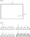
- FIG. 2 is a plan view showing a pattern 16a of micro protrusions existing on the adhesion reduction layer 16 of FIG. 1 .
- FIG. 3 is a cross-sectional view showing examples of the micro protrusions of the pattern of FIG. 1 .
- it does not show a cross-sectional view of a strict meaning, and there may be components that may not appear in the drawings for convenience of explanation.
- the first display device 100 is configured by sequentially stacking a display 10, a bonding layer 12, a touch screen 14, an adhesion reduction layer 16, a detachable layer 18, and a window 20.
- the detachable layer 18 and the window 20 are referred to as a first window structure 22 together.
- the display 10 includes a liquid crystal display (LCD), an organic light emitting diode (OLED), an electrophoretic display (EPD) and the like, and quantum dots are also utilized.
- the bonding layer 12 firmly bonds the touch screen 14 to the display 10.
- a thermosetting adhesive or an ultraviolet curable adhesive may be used.
- the bonding layer 12 is not limited thereto, and an OCA tape or the like may also be used.
- the touch screen 14 has a conductive pattern formed on one side or both sides of an insulating layer made of metal oxide or plastic.
- the metal oxide is mainly applied to the conductive pattern, and the metal oxide includes ITO, ATO, ZnO, Cu, conductive polymer, silver nanowire or the like.
- the window 20 may use a transparent material without limit.
- the window 20 may include a glass substrate or a plastic substrate.
- the glass substrate may be tempered glass
- the plastic substrate may include any one or any one or more among polyethylene terephthalate (PET), polyethylene naphthalate (PEN), polyether sulfone (PES), polyimide (PI), polyarylate (PAR), polycarbonate (PC), polymethyl methacrylate (PJl!lMA), and cycloolefin copolymer (COC).
- PET polyethylene terephthalate
- PEN polyethylene naphthalate
- PES polyether sulfone
- PI polyimide
- PAR polyarylate
- PC polycarbonate
- PJl!lMA polymethyl methacrylate
- COC cycloolefin copolymer
- the window 20 may also be a stacked structure in which the tempered glass and the plastic substrate are formed as multiple layers.
- the window 20 may have a print layer transparent or implementing various functions.
- the print layer may apply any one or any one or more coatings among transparent, translucent and color coatings.
- the print layer may be formed by silk printing, inkjet printing using UV, inkjet printing using thermosetting, or transfer printing.
- a functional coating layer such as anti-fingerprint coating, antimicrobial coating, or antiscratch coating may be formed on the window 20.
- the functional coating layer may be formed by wet coating of applying a coating liquid or dry coating such as deposition.
- the characteristics such as shielding, anti-reflection, blue light blocking, electromagnetic wave blocking, privacy and the like may be provided on the bottom of the glass substrate or the plastic substrate of the window 20.
- an opening for exposing a button, a camera, a speaker or the like may be formed in the window 20.
- an adhesion reduction layer 16 is located on the touch screen 14 to facilitate attachment and detachment of the first window structure 22.
- the adhesion reduction layer 16 increases the slip property by lowering frictional force.
- the first window structure 22 may be easily attached to and detached from the touch screen 14 by the adhesion reduction layer 16.
- the adhesion reduction layer 16 uses a coating material of fluorine-based resin or silicon-based resin.
- the adhesion is reduction layer 16 formed by depositing titania (Ti02) or silica (Si02) on the touch screen 14 and then coating a fluorine-based resin or a silicon-based resin on the deposited touch screen 14. At this point, the fluorine-based resin or the silicon-based resin may be formed in an easy cleaning coating (ECC) method.
- ECC easy cleaning coating
- the adhesion reduction layer 16 If the adhesion reduction layer 16 is applied, generation of bubbles can be suppressed more effectively when the window 20 is attached. In addition, the adhesion reduction layer 16 allows a consumer to easily attach and detach the first window structure 22 by himself or herself without a tool.
- the detachable layer 18 has an adhesive force of about 0.lgf/25mm to 500gf/25mm.
- the detachable layer 18 is made of various materials within the scope of the present invention, more concretely, any one selected among an adhesive made by mixing a crosslinking agent with a thermosetting resin, i.e., an acrylic polymer, a silicon polymer or a urethane polymers, or an ultraviolet curable resin, a mixture of these, and a copolymer of these.
- the adhesive force of the detachable layer 18 is about 0.lgf/25mm to 500gf/25mm
- the detachable layer 18 has a self-adhesive force.
- the self-adhesive force is a property of the detachable layer 18 adhering itself without bubbles by simply putting the detachable layer 18 on the touch screen 14.
- the adhesion reduction layer 16 when the adhesion reduction layer 16 is applied to the touch screen 14, the self-adhesive force is improved more than when there is no adhesion reduction layer 16.
- the adhesive force according to an embodiment of the present invention may vary depending on the presence of the adhesion reduction layer 16.
- the adhesive force is 0.5gf/25mm to 500gf/25mm when the adhesion reduction layer 16 exists, whereas the adhesive force is 0.lgf/25mm to 200gf/25mm when the adhesion reduction layer 16 does not exist. If there exists an adhesion reduction layer 16 when a detachment layer 18 of the same material and thickness is provided, it is easier to attach the first window structure 22 without bubbles. In addition, owing to the effect of the adhesion reduction layer 16, separation of the first window structure 22 occurs relatively easily.
- the detachable layer 18 may be a detachable fluid layer in the form of a pocket containing a fluid, or a detachable pattern that is partially cured to form a pattern.
- the detachable fluid layer includes a bonding surface bonded to a transparent sheet in the form of a pocket, an adhesive surface attached to a display component, and a side surface located between the bonding surface and the adhesive surface to form a side wall, and the pocket provides a space in which a fluid is filled.
- the detachable pattern is a pattern including an adhesive layer having an adhesive force of about O.lgf/25mm to 500gf/25mm and a cured layer formed by curing the adhesive layer.
- a pattern 16a formed of micro protrusions exists in the adhesion reduction layer 16.
- the pattern 16a expresses a logo, a name, a product specification or the like as a character or a figure, and particularly refers to information requested by a customer.
- the authenticity and engraved pattern of at least one among a window, a touch screen and a display obtained through different channels may be confirmed.
- Other part of the adhesion reduction layer 16 than the pattern 16a is in a state without having micro protrusions.
- the pattern 16a is in a translucent state when it is separated from the detachable layer 18, and when the detachable layer 18 is attached to the adhesion reduction layer 16, the pattern 16a disappears and the adhesion reduction layer 16 becomes transparent.
- the pattern 16a of the adhesion reduction layer 16 is formed of various micro protrusions.
- micro protrusions having a cross section formed in any one shape selected among a rectangle (a), a triangle (b) and a circle (c), or made of beads or beads and a binder (d) are presented as examples. That is, the cross section of the micro protrusions a, b, c and d may have an angle, a curvature or a combination of these.
- the pattern 16a is translucent, and transmittance of light is lowered. As the transmittance of the pattern 16a formed of micro protrusions having reduced transmittance is lowered, the adhesion reduction layer 16 is visually distinguished from the transparent adhesive reduction layer 16 without having micro protrusions.
- the adhesive of the detachable layer 18 penetrates into the space between the micro protrusions, and the translucent screen becomes transparent. Accordingly, although the adhesion reduction layer 16 having micro protrusions formed thereon is used, the clarity of screen in the transparent state may be continuously maintained.
- the micro protrusions are formed in various ways.
- the micro protrusions may be formed by mixing translucent beads such as silica or the like with UV or thermosetting resin or the like, and coating and curing the pattern 16a.
- the micro protrusions may be formed by pressing a sheet or roll mold engraved with micro protrusions on the pattern 16a coated with UV or thermosetting resin, and curing the pattern 16a.
- the pattern 16a having micro protrusions may be manufactured by transferring a film or a sheet coated with UV or thermosetting resin.
- the pattern 16a may be formed by shaping using a mold having a shape corresponding to the micro protrusions.
- the pattern 16a may be formed by coating resin or the like after masking or forming micro protrusions through exposure or etching, and removing the mask.
- the pattern 16a may be formed by radiating laser beam on the surface of the adhesion reduction layer 16.
- the pattern 16a may be formed by printing on the surface of the adhesion reduction layer 16 using UV or thermosetting ink.
- the pattern 16a may be formed on the surface by applying a physical impact on the surface of the adhesion reduction layer 16.
- the first window structure 22 of the present invention is separately manufactured and protected by a release film.
- the release film is removed to attach the first window structure 22 to the touch screen 14 or the adhesion reduction layer 16.
- the detachable layer 18 is exposed.
- a display mounted with the window 20 may be completed.
- the first window structure 22 ( 20) is manually separated, and a new first window structure 22 may be attached.
- FIG. 4 is a cross-sectional view showing a second display device 200 including a first window structure 22 that can be attached and detached according to an embodiment of the present invention. However, it does not show a cross-sectional view of a strict meaning, and there may be components that may not appear in the cross-sectional view for convenience of explanation.
- the second display device 200 is the same as the first display device 100 except that the bonding layer 12 does not exist.
- the matters overlapped with the above description will be omitted or briefly described.
- a display 10, a touch screen 14, an adhesion reduction layer 16 having a pattern 16a, and a first window structure 22 configure sequential layers.
- the touch screen 14 is manufactured by forming a conductive pattern directly on the display 10. That is, the touch screen 14 is formed together with the conductive pattern formed on the display 10.
- the first window structure 22 includes the detachable layer 18 described above.
- the pattern 16a is in a translucent state when it is separated from the detachable layer 18, and when the detachable layer 18 is attached to the adhesion reduction layer 16, the pattern 16a disappears and the adhesion reduction layer 16 becomes transparent.
- the second display device 200 may be provided with an adhesion reduction layer 16, like the first display device 100.
- the materials, functions and the like of the adhesion reduction layer 16 are the same as those described in the first display device 100.
- the adhesive force according to an embodiment of the present invention may vary depending on the presence of the adhesion reduction layer 16.
- the adhesive force is 0.5gf/25mm to 500gf/25mm when the adhesion reduction layer 16 exists, whereas the adhesive force is 0.lgf/25mm to 200gf/25mm when the adhesion reduction layer 16 does not exist. If there exists an adhesion reduction layer 16 when a detachment layer 18 of the same material and thickness is provided, it is easy to attach the first window structure 22 without bubbles.
- an additional component for providing various functions may be further provided between the window 20 and the detachable layer 18 of the first window structure 22 according to an embodiment of the present invention.
- the additional component may include an optically clear adhesive (OCA) layer, a shatterproof layer, and the like, and if necessary, a print layer and a functional coating layer may be appropriately formed.
- OCA optically clear adhesive
- the detachable layer 18 may be formed on the transparent synthetic resin film. Since such an additional component is already well known, detailed description thereof will be omitted.
- FIG. 5 is a cross-sectional view showing a third display device 300 including a second window structure 26 that can be attached and detached according to an embodiment of the present invention. However, it does not show a cross-sectional view of a strict meaning, and there may be components that may not appear in the cross-sectional view for convenience of explanation.
- the third display device 300 is the same as the first display device 100 except that a touch screen cover layer 24 is adopted. Accordingly, the detailed description of the same reference numerals will be omitted.
- the second window structure 26 may further include additional components, as is described in the first window structure 22.
- the third display device 300 may be implemented by sequentially stacking a display 10, a bonding layer 12, a touch screen 14, a cover layer 24, an adhesion reduction layer 16 having a pattern 16a, a detachable layer 18, and a window 20.
- the display 10 may be directly bonded to the touch screen 14 without the bonding layer 12, like the second display device 200.
- a conductive pattern for forming the touch screen 14 is disposed on the top or bottom of the cover layer 24.
- the cover layer 24 may be regarded as a part of the touch screen 14.
- the cover layer 24 prevents the touch screen 14 from being damaged by impact or contamination.
- the third display device 300 configures the touch screen 14 by forming a conductive pattern directly on the display 10. In this case, the touch screen cover layer 24 may be positioned on the top of the display 10.
- the cover layer 24 When the cover layer 24 is covered with the second window structure 26, it is positioned inside the third display device 300. Since the cover layer 24 ( 22) is positioned inside, there is no worry that the cover layer 24 is exposed to the outside of the third display device 300 and damaged by impact or the like.
- the cover layer 24 may include a print layer or a functional coating layer, and may beautify the third display device 300 through various designs or translucence. In addition, the cover layer 24 may exclude the effect of windings and steps generated by various patterns, circuits or the like of the touch screen 14. When the effect of windings and steps disappears, attachment and detachment by the detachment layer 18 becomes easier.
- the cover layer 24 may use a transparent material without limit.
- the window 20 may include a glass substrate or a plastic substrate.
- the glass substrate may be tempered glass or untempered glass, and in addition, the plastic substrate may include any one or more among polyethylene terephthalate (PET), polyethylene naphthalate (PEN), polyether sulfone (PES), polyimide (PI), polyarylate (PAR), polycarbonate (PC), polymethyl methacrylate (PMMA), and cycloolefin copolymer (COC).
- PET polyethylene terephthalate
- PEN polyethylene naphthalate
- PES polyether sulfone
- PI polyimide
- PAR polyarylate
- PC polycarbonate
- PMMA polymethyl methacrylate
- COC cycloolefin copolymer
- the thickness of the cover layer 24 is sufficient if the touch screen 14 ( 20) is not damaged in the process of using the third display device 300.
- the third display device 300 may be provided with an adhesion reduction layer 16, like the first display device 100.
- the materials, functions and the like of the adhesion reduction layer 16 are the same as those described in the first display device 100.
- the adhesive force according to an embodiment of the present invention may vary depending on the presence of the adhesion reduction layer 16.
- the adhesive force is 0.5gf/25mm to 500gf/25mm when the adhesion reduction layer 16 exists, whereas the adhesive force is 0.1gf/25mm to 200gf/25mm when the adhesion reduction layer 16 does not exist. If there exists an adhesion reduction layer 16 when a detachment layer 18 of the same material and thickness is provided, it is easy to attach the second window structure 26 without bubbles. In addition, owing to the effect of the adhesion reduction layer 16, separation of the second window structure 26 occurs relatively easily.
- the detachable layer 18 When the adhesive force of the detachable layer 18 is about 0.1gf/25mm to 500gf/25mm, the detachable layer 18 has self-adhesive force.
- the self-adhesive force is a property of the detachable layer 18 adhering itself without bubblesby simply putting the detachable layer 18 on the cover layer 24.
- the adhesion reduction layer 16 when the adhesion reduction layer 16 is applied to the cover layer 24, the self-adhesive force is improved more than when there is no adhesion reduction layer 16.
- the pattern 16a is in a translucent state when it is separated from the detachable layer 18, and when the detachable layer 18 is attached to the adhesion reduction layer 16, the pattern 16a disappears and the adhesion reduction layer 16 becomes transparent.
- the window structure may be replaced by selecting and attaching a new window structure. Specifically, the broken window structure is removed and replaced by attaching a new window structure. A customer himself or herself may manually perform the process of replacing the window structure, and the time required for replacing the window structure is very short. In addition, since only the window structure needs to be removed, recycle of the display device is easy. Furthermore, since the window structure is attached and detached, it can be easily attached without bubbles. Since a manufacturer only needs to manufacture only the parts other than the window structure and does not need to perform an adhering process, the manufacturing process is simplified.
- FIG. 6 is a cross-sectional view showing a fourth display 400 device including a third window structure 30 that can be attached and detached according to an embodiment of the present invention. However, it does not show a cross-sectional view of a strict meaning, and there may be components that may not appear in the cross-sectional view for convenience of explanation.
- the fourth display device 400 is basically the same as the first display device 100 except that the position of each layer is changed.
- the matters overlapped with the above description will be omitted or briefly described.
- the fourth display apparatus 400 is configured by sequentially stacking a display 10, an adhesion reduction layer 16 having a pattern 16a, a detachable layer 18, a touch screen 14, a bonding layer 12, and a window 20.
- the window 20, the bonding layer 12, the touch screen 14, and the detachable layer 18 configure the third window structure 30.
- the display 10 includes a liquid crystal display (LCD), an organic light emitting diode (OLED), an electrophoretic display (EPD) and the like, and quantum dots are also utilized.
- a thermosetting adhesive or an ultraviolet curable adhesive may be used for the bonding layer 12.
- the bonding layer 12 is not limited thereto, and an OCA tape or the like may also be used.
- the touch screen 14 has conductive patterns formed on one side or both sides of an insulating layer made of metal oxide or plastic.
- Metal oxide is mainly applied to the conductive pattern, and the metal oxide includes ITO, ATO, ZnO, Cu, conductive polymer, silver nanowire or the like.
- the adhesion reduction layer 16 is located on the display 10 to facilitate attachment and detachment of the third window structure 30.
- the adhesion reduction layer 16 increases the slip property by increasing the contact angle.
- the third window structure 30 may be easily attached to and detached from the touch screen 14 by the adhesion reduction layer 16.
- the adhesion reduction layer 16 uses a coating material of fluorine-based resin or silicon-based resin.
- the adhesion reduction layer 16 is formed by depositing titania (TiO2) or silica (Si02) on the display 10, and then coating a fluorine-based resin or a silicon-based resin on the deposited display 10. At this point, the fluorine-based resin or the silicon-based resin may be formed in an easy cleaning coating (ECC) method.
- ECC easy cleaning coating
- adhesion reduction layer 16 If the adhesion reduction layer 16 is applied, generation of bubbles can be suppressed more effectively when the touch screen 14 is attached.
- the adhesion reduction layer 16 ( pattern 60) allows a consumer to easily attach and detach the third window structure 30 by himself or herself without a tool.
- the detachable layer 18 When the adhesive force of the detachable layer 18 is about 0.lgf/25mm to 500gf/25mm, the detachable layer 18 has self-adhesive force.
- the self-adhesive force is a property of the detachable layer 18 adhering itself without bubbles by simply putting the detachable layer 18 on the touch screen 14.
- the adhesion reduction layer 16 when the adhesion reduction layer 16 is applied to the display 10, the self-adhesive force is improved more than when there is no adhesion reduction layer 16.
- the adhesive force according to an embodiment of the present invention may vary depending on the presence of the adhesion reduction layer 16.
- the adhesive force is 0.5gf/25mm to 500gf/25mm when the adhesion reduction layer 16 exists. If the adhesion reduction layer 16 does not exist, the adhesive force is 0.lgf/25mm to 200gf/25mm. If there exists an adhesion reduction layer 16 when a detachment layer 18 of the same material and thickness is provided, it is easy to attach the third window structure 30 without bubbles. In addition, owing to the effect of the adhesion reduction layer 16, separation of the third window structure 30 occurs relatively easily.
- the third window structure 30 of the present invention is separately manufactured and protected by a release film.
- the release film is removed to attach the third window structure 30 to the display 10.
- the detachable layer 18 is exposed.
- the third window structure 30 having the exposed detachable layer 18 is manually attached to the display 10, a display mounted with the window 20 may be completed. Accordingly, unlike the prior art, a precise bonding process is not required.
- the third window structure 30 is damaged or to be replaced, the third window structure 30 is manually separated, and a new third window structure 30 may be attached.
- the pattern 16a is in a translucent state when it is separated from the detachable layer 18, and when the detachable layer 18 is attached to the adhesion reduction layer 16, the pattern 16a disappears, and the adhesion reduction layer 16 becomes transparent.
- FIG. 7 is a cross-sectional view showing a fifth display device 500 including a fourth window structure 34 that can be attached and detached according to an embodiment of the present invention. However, it does not show a cross-sectional view of a strict meaning, and there may be components that may not appear in the cross-sectional view for convenience of explanation.
- the fifth display device 500 is the same as the first display device 100 except that the bonding layer 12 is replaced with a detachable layer 32.
- the matters overlapped with the above description will be omitted or briefly described.
- a display 10, an adhesion reduction layer 16 having a pattern 16a, a detachable layer 18, a touch screen 14, a detachable layer 32, and a window 20 are sequentially stacked in the fifth display device 500.
- the window 20, the detachable layer 32, the touch screen 14, and the detachable layer 18 configure the fourth window structure 34.
- the function and role of the detachable layer 32 are the same as those of the detachable layer 18, a different reference numeral is assigned since the position is different.
- the fourth window structure 34 is attached to and detached from the display 10 by the detachable layer 18.
- the detachable layer 18 may be attached to the display 10 while the release film is removed.
- the fourth window structure 34 may be attached to and detached from the touch screen 14 by the detachable layer 32.
- the fifth ( fourth) window structure 34 includes the detachable layer 18 and the detachable layer 32 that can be attached to and detached from the display 10 and the touch screen 20 ( 14), respectively.
- the pattern 16a is in a translucent state when it is separated from the detachable layer 18, and when the detachable layer 18 is attached to the adhesion reduction layer 16, the pattern 16a disappears, and the adhesion reduction layer 16 becomes transparent.
- the 32 is detachable layer an acrylic polymer, a silicon polymer, a urethane polymer, an adhesive made by mixing a crosslinking agent with an ultraviolet curable resin, a mixture thereof, or a copolymer thereof.
- the detachable layer 32 may be a single layer or a multilayer made of different materials in each layer, and at least one may be a single layer. In the multilayer, a material which forms each layer may be appropriately selected according to the environment in which the detachable layer 32 of the present invention is used. Thickness of the detachable layer 32 is acceptable if the adhesion is sufficient, and thickness of 10 to 200 micrometers is preferable. It is apparent that the thickness can be obtained through repeated experiments by those skilled in the art.
- an additional component for providing various functions may be further provided between the window 20 and the detachable layer 32 or between the touch screen 14 and the detachable layer 18 of the third and fourth window structures 30 and 34 ( 32) according to an embodiment of the present invention.
- the additional component may include an optically clear adhesive (OCA) layer, a shatterproof layer, and the like, and if necessary, a print layer and a functional coating layer may be appropriately formed.
- OCA optically clear adhesive
- the detachable layer 18 may be formed on the transparent synthetic resin film. Since such an additional component is already well known, detailed description thereof will be omitted.
- FIG. 7 is a cross-sectional view showing a sixth display device 600 including a fifth window structure 36 that can be attached and detached according to an embodiment of the present invention. However, it does not show a cross-sectional view of a strict meaning, and there may be components that may not appear in the cross-sectional view for convenience of explanation.
- the sixth display device 600 is the same as the fourth display device 400 except that the bonding layer 12 is not provided. Accordingly, the detailed description of the same reference numerals will be omitted.
- the fifth window structure 36 may further include additional components, as is described in the third window structure 30.
- the sixth display device 600 is configured by stacking a display 10, an adhesion reduction layer 16 having a pattern 16a, a detachable layer 18, a touch screen 14, and a window 20.
- the window 20, the touch screen 14, and the detachable layer 18 configure the fifth window structure 36.
- the touch screen 14 is manufactured by forming a conductive pattern directly under the window 20. That is, the touch screen 14 is formed together with the conductive pattern formed under the window 20.
- the sixth display device 600 may be provided with an adhesion reduction layer 16, like the fourth display device 400.
- the materials, functions and the like of the adhesion reduction layer 16 are the same as those described in the fourth display device 400.
- the adhesive force according to an embodiment of the present invention may vary depending on the presence of the adhesion reduction layer 16.
- the adhesive force is 0.5gf/25mm to 500gf/25mm when the adhesion reduction layer 16 exists, whereas the adhesive force is 0.lgf/25mm to 200gf/25mm when the adhesion reduction layer 16 does not exist. If there exists an adhesion reduction layer 16 when a detachment layer 18 of the same material and thickness is provided, it is easy to attach the fifth window structure 36 without bubbles. In addition, owing to the effect of the adhesion reduction layer 16, separation of the fifth window structure 36 occurs relatively easily.
- the detachable layer 18 has a self-adhesive force.
- the self-adhesive force is a property of the detachable layer 18 adhering itself without bubbles by simply putting the detachable layer 18 on the display 10.
- the adhesion reduction layer 16 is applied to the display 10
- the self-adhesive force is improved more than when there is no adhesion reduction layer 16.
- the pattern 16a is in a translucent state when it is separated from the detachable layer 18, and when the detachable layer 18 is attached to the adhesion reduction layer 16, the pattern 16a disappears, and the adhesion reduction layer 16 becomes transparent.
- connection units may be made to face each other in predetermined areas of the display 10 and the touch screen 14, respectively.
- part of the detachable layer 18 of the touch screen 14 may be removed.
- the connection units are connected to each other. In this manner, connections of the first to sixth display devices 100, 200, 300, 400, 500 and 600 may be implemented.
- the window structure maybe replaced by selecting and attaching a new window structure. Specifically, the broken window structure is removed and replaced by attaching a new window structure.
- a customer himself or herself may perform theprocess of replacing the window structure, and the time required for replacing the window structure is very short.
- recycle of the display device is easy.
- the window structure is attached and detached by adhesion, it can be easily attached without bubbles. Since a manufacturer only needs to manufacture only the parts other than the window structure and does not need to perform an adhering process, the manufacturing process is simplified. Particularly, when an adhesion reduction layer ( pattern) exists, it is easier to attach the window structure without bubbles, and owing to the effect of the adhesion reduction layer ( pattern), separation of the window structure occurs relatively easily.
- the appearance of the display device of the present invention can be diversely designed.
- the display device of the present invention may be designed to have a beautiful shape, various colors and patterns, and the like. This is since that when an original window structure is separated and a new structure is attached, the appearance of the window structure can be changed in a desired design. Conventionally, it needs to remove adhesion of the window structure and reattach a new window structure to change the design.
- the design is changed by detaching an existing window structure and attaching a new window structure. Accordingly, unlike a conventional window structure, the window structure of the present invention is not an essential component fixed to a display device and may be treated as a disposable component that can be attached and detached as needed. If the design is diversified in this way, the manufacturer of the display device does not need to provide a service corresponding to the design later.
- the adhesion reduction layer 16 is applied to facilitate attachment and detachment of a detachable layer having an adhesive force of O.lgf/25mm to 500gf/25mm.
- a pattern 16a configured of micro protrusions is formed on the adhesion reduction layer 16, the authenticity and engraved pattern of at least any one product among a window, a touch screen and a display that are freely attached and detached, and obtained through different channels can be confirmed.
- the display device of the present invention may satisfy desires of consumers. Furthermore, since anyone may easily replace a window, a touch screen and a window and touch screen by attaching and detaching, it can be treated as a disposable component rather than an essential component fixed to the display device.
Landscapes
- Engineering & Computer Science (AREA)
- Physics & Mathematics (AREA)
- General Engineering & Computer Science (AREA)
- Theoretical Computer Science (AREA)
- Chemical & Material Sciences (AREA)
- General Physics & Mathematics (AREA)
- Human Computer Interaction (AREA)
- Organic Chemistry (AREA)
- Health & Medical Sciences (AREA)
- Chemical Kinetics & Catalysis (AREA)
- Medicinal Chemistry (AREA)
- Polymers & Plastics (AREA)
- Nonlinear Science (AREA)
- Crystallography & Structural Chemistry (AREA)
- Optics & Photonics (AREA)
- Mathematical Physics (AREA)
- Laminated Bodies (AREA)
- Devices For Indicating Variable Information By Combining Individual Elements (AREA)
- Position Input By Displaying (AREA)
- Adhesive Tapes (AREA)
Claims (5)
- Anzeigevorrichtung (100, 200, 300, 400, 500, 600), die ein Fenster (20) und eine Anzeige (10) beinhaltet, die einen Berührungsbildschirm (14) beinhaltet, und eine Haftreduzierungsschicht (16) beinhaltet;wobei die Vorrichtung Folgendes umfasst:eine ablösbare Schicht (18), die sich auf einem beliebigen von dem Fenster (20), dem Berührungsbildschirm (14) und der Anzeige (10) befindet und eine Haftkraft von 0,1 x 0,00980664999999998 N / 25 mm bis 500 x 0,00980664999999998 N / 25 mm aufweist;wobei die ablösbare Schicht eine beliebige ausgewählt aus einem Klebstoff hergestellt durch Mischen eines Vernetzungsmittels mit einem wärmehärtbaren Harz, d. h. einem Acrylpolymer, einem Silikonpolymer oder einem Urethanpolymeren, oder einem UV-härtbaren Harz, einer Mischung von diesen und einem Copolymer von diesen ist,wobei die Haftreduzierungsschicht ein Harz auf Fluorbasis oder ein Harz auf Siliziumbasis enthält,dadurch gekennzeichnet, dass:die Haftreduzierungsschicht (16) ein Mikrovorsprungmuster (16a) aufweist und das Mikrovorsprungmuster (16a) aus Mikrovorsprüngen auf einem Abschnitt der Haftreduzierungsschicht (16) gebildet ist, die positioniert ist, um der ablösbaren Schicht (18) zugewandt zu sein, um Haftkraft der ablösbaren Schicht (18) in einem beliebigen von dem Fenster (20), dem Berührungsbildschirm (14) und der Anzeige (10) zu reduzieren,wobei die ablösbare Schicht (18) in das Mikrovorsprungmuster (16a) der Haftreduzierungsschicht (16) eindringt, um die Haftreduzierungsschicht (16) transparent zu machen, undwobei das Mikrovorsprungmuster (16a) ein Zeichen, eine Figur oder eine Kombination von diesen ist.
- Vorrichtung nach Anspruch 1, wobei:die Haftreduzierungsschicht (16) eine Abscheidungsschicht hergestellt aus Titandioxid (TiO2) oder Siliziumdioxid (SiO2) beinhaltet, undeine Schicht, die ein Harz auf Fluorbasis oder ein Harz auf Siliziumbasis enthält, sich auf der Abscheidungsschicht befindet.
- Vorrichtung nach Anspruch 1, wobei die ablösbare Schicht (18) eine Haftkraft von 0,5 gf/25 mm bis 500 gf/25 mm durch die Haftreduzierungsschicht (16) aufweist.
- Vorrichtung nach Anspruch 1, wobei ein Querschnitt des Mikrovorsprungmusters (16a) einen Winkel, eine Krümmung oder eine Kombination von diesen aufweist.
- Vorrichtung nach Anspruch 1, wobei das Mikrovorsprungmuster (16a) in einer Linienform, einer Gitterform, einer Inselform oder einer Kombination von diesen angeordnet ist.
Applications Claiming Priority (3)
| Application Number | Priority Date | Filing Date | Title |
|---|---|---|---|
| KR20160127309 | 2016-10-03 | ||
| KR1020170123042A KR102098453B1 (ko) | 2016-10-03 | 2017-09-23 | 미세돌기 문양을 가진 접착감소층을 포함하는 디스플레이 장치 |
| PCT/KR2018/009985 WO2019059551A1 (ko) | 2016-10-03 | 2018-08-29 | 미세돌기 문양을 가진 접착감소층을 포함하는 디스플레이 장치 |
Publications (3)
| Publication Number | Publication Date |
|---|---|
| EP3686715A1 EP3686715A1 (de) | 2020-07-29 |
| EP3686715A4 EP3686715A4 (de) | 2020-10-28 |
| EP3686715B1 true EP3686715B1 (de) | 2022-09-21 |
Family
ID=61976033
Family Applications (1)
| Application Number | Title | Priority Date | Filing Date |
|---|---|---|---|
| EP18858672.1A Active EP3686715B1 (de) | 2016-10-03 | 2018-08-29 | Anzeigevorrichtung mit adhäsionsverringerungsschicht mit mikrovorsprungmuster |
Country Status (6)
| Country | Link |
|---|---|
| US (1) | US11301070B2 (de) |
| EP (1) | EP3686715B1 (de) |
| JP (1) | JP6975491B2 (de) |
| KR (1) | KR102098453B1 (de) |
| CN (1) | CN111133406A (de) |
| WO (1) | WO2019059551A1 (de) |
Families Citing this family (6)
| Publication number | Priority date | Publication date | Assignee | Title |
|---|---|---|---|---|
| KR102241293B1 (ko) * | 2018-05-14 | 2021-04-16 | 김영수 | 점착조절층을 이용한 표시장치 |
| KR102535004B1 (ko) * | 2018-07-27 | 2023-05-22 | 삼성디스플레이 주식회사 | 압력 센서를 포함하는 표시 장치 |
| KR102241276B1 (ko) * | 2018-08-20 | 2021-04-16 | 김영수 | 일체형 커버를 포함하는 탈부착 표시장치 |
| KR102241233B1 (ko) * | 2018-11-29 | 2021-04-16 | 주식회사 맥스젠테크놀로지 | 탈부착 윈도우가 탈부착되는 표시장치의 윈도우 분리형 모듈 |
| KR102638658B1 (ko) * | 2019-09-06 | 2024-02-21 | 삼성전자주식회사 | 불연속 패턴을 가지는 레이어를 포함하는 디스플레이 및 그를 포함하는 전자 장치 |
| KR102774689B1 (ko) * | 2020-05-26 | 2025-03-06 | 삼성디스플레이 주식회사 | 폴더블 표시장치 |
Citations (1)
| Publication number | Priority date | Publication date | Assignee | Title |
|---|---|---|---|---|
| JP2006344163A (ja) * | 2005-06-10 | 2006-12-21 | Nissha Printing Co Ltd | 静電容量型タッチパネル |
Family Cites Families (8)
| Publication number | Priority date | Publication date | Assignee | Title |
|---|---|---|---|---|
| JP5011676B2 (ja) * | 2005-08-12 | 2012-08-29 | 株式会社日立製作所 | 表示装置を備える機器 |
| JP2014224919A (ja) * | 2013-05-16 | 2014-12-04 | 日本電気株式会社 | 表示装置 |
| KR101350428B1 (ko) | 2013-06-21 | 2014-01-14 | 에스지글로벌 주식회사 | 터치스크린용 디스플레이 유닛 및 이의 제조방법 |
| KR20150034829A (ko) * | 2013-08-30 | 2015-04-06 | 주식회사 엔씰텍 | 플렉시블 정보 표시 소자 제조용 지지 기판, 이의 제조 방법, 이를 이용하여 제조된 플렉시블 정보 표시 소자 및 이의 제조방법 |
| KR101512185B1 (ko) * | 2014-08-19 | 2015-04-16 | 덕산에스지 주식회사 | 디스플레이 기능을 가지는 패널 |
| KR101574923B1 (ko) * | 2015-01-20 | 2015-12-04 | 김영수 | 탈부착이 가능한 윈도우를 포함하는 디스플레이 장치 및 그 탈부착 방법 |
| JP6460525B2 (ja) * | 2015-01-30 | 2019-01-30 | 藤森工業株式会社 | 接着性樹脂層、接着性樹脂フィルム、積層体及び積層体の製造方法 |
| KR101675225B1 (ko) | 2015-04-08 | 2016-11-10 | 김영수 | 탈부착층을 가진 디스플레이 장치 및 그 제조방법 |
-
2017
- 2017-09-23 KR KR1020170123042A patent/KR102098453B1/ko not_active Expired - Fee Related
-
2018
- 2018-08-29 CN CN201880060709.7A patent/CN111133406A/zh active Pending
- 2018-08-29 WO PCT/KR2018/009985 patent/WO2019059551A1/ko not_active Ceased
- 2018-08-29 EP EP18858672.1A patent/EP3686715B1/de active Active
- 2018-08-29 US US16/649,383 patent/US11301070B2/en active Active
- 2018-08-29 JP JP2020516411A patent/JP6975491B2/ja not_active Expired - Fee Related
Patent Citations (1)
| Publication number | Priority date | Publication date | Assignee | Title |
|---|---|---|---|---|
| JP2006344163A (ja) * | 2005-06-10 | 2006-12-21 | Nissha Printing Co Ltd | 静電容量型タッチパネル |
Also Published As
| Publication number | Publication date |
|---|---|
| KR102098453B1 (ko) | 2020-04-07 |
| US20200301534A1 (en) | 2020-09-24 |
| EP3686715A4 (de) | 2020-10-28 |
| US11301070B2 (en) | 2022-04-12 |
| CN111133406A (zh) | 2020-05-08 |
| JP2020534578A (ja) | 2020-11-26 |
| KR20180037109A (ko) | 2018-04-11 |
| EP3686715A1 (de) | 2020-07-29 |
| JP6975491B2 (ja) | 2021-12-01 |
| WO2019059551A1 (ko) | 2019-03-28 |
Similar Documents
| Publication | Publication Date | Title |
|---|---|---|
| EP3686715B1 (de) | Anzeigevorrichtung mit adhäsionsverringerungsschicht mit mikrovorsprungmuster | |
| EP3521982B1 (de) | Anzeigevorrichtung mit feinem höcker zur einstellung von befestigung und entfernung sowie herstellungsverfahren dafür | |
| KR101574923B1 (ko) | 탈부착이 가능한 윈도우를 포함하는 디스플레이 장치 및 그 탈부착 방법 | |
| KR101675225B1 (ko) | 탈부착층을 가진 디스플레이 장치 및 그 제조방법 | |
| EP3686716B1 (de) | Anzeigevorrichtung mit anbringbarem/abnehmbarem muster | |
| KR102146151B1 (ko) | 표면개질 탈부착 시트를 포함하는 디스플레이 장치 | |
| KR20180037088A (ko) | 탈부착층을 포함하는 디스플레이 장치 및 그 제조방법 | |
| KR20180026830A (ko) | 탈부착층을 가진 디스플레이 장치 | |
| EP3293568A1 (de) | Anzeigevorrichtung mit abnehmbarer schicht und verfahren zur herstellung davon | |
| JP6330871B2 (ja) | 着脱層を有するディスプレイ装置、及びその製造方法{Apparatus of display having detachable layer and method of manufacturing the display} | |
| KR20180103428A (ko) | 곡면 디스플레이 장치용 광학필름 및 그 제조방법 | |
| KR20180037103A (ko) | 탈부착 시트를 포함하는 디스플레이 장치 | |
| KR102144652B1 (ko) | 탈부착 패턴을 가진 디스플레이 장치 | |
| KR20200005996A (ko) | 보호필름을 위한 미세돌기를 포함하는 표시장치 | |
| KR102437333B1 (ko) | 복합커버층을 포함하는 탈부착 표시장치 | |
| WO2018066853A1 (ko) | 탈부착 조절을 위한 미세돌기를 포함하는 디스플레이 장치 및 그 제조방법 | |
| KR20180119430A (ko) | 문양이 인쇄된 보호시트 제조방법 및 그에 의해 제조된 보호시트 |
Legal Events
| Date | Code | Title | Description |
|---|---|---|---|
| STAA | Information on the status of an ep patent application or granted ep patent |
Free format text: STATUS: THE INTERNATIONAL PUBLICATION HAS BEEN MADE |
|
| PUAI | Public reference made under article 153(3) epc to a published international application that has entered the european phase |
Free format text: ORIGINAL CODE: 0009012 |
|
| STAA | Information on the status of an ep patent application or granted ep patent |
Free format text: STATUS: REQUEST FOR EXAMINATION WAS MADE |
|
| 17P | Request for examination filed |
Effective date: 20200422 |
|
| AK | Designated contracting states |
Kind code of ref document: A1 Designated state(s): AL AT BE BG CH CY CZ DE DK EE ES FI FR GB GR HR HU IE IS IT LI LT LU LV MC MK MT NL NO PL PT RO RS SE SI SK SM TR |
|
| AX | Request for extension of the european patent |
Extension state: BA ME |
|
| A4 | Supplementary search report drawn up and despatched |
Effective date: 20200925 |
|
| RIC1 | Information provided on ipc code assigned before grant |
Ipc: G02F 1/13 20060101ALI20200921BHEP Ipc: B32B 7/06 20190101ALI20200921BHEP Ipc: B32B 3/30 20060101ALI20200921BHEP Ipc: G06F 3/041 20060101AFI20200921BHEP |
|
| DAV | Request for validation of the european patent (deleted) | ||
| DAX | Request for extension of the european patent (deleted) | ||
| STAA | Information on the status of an ep patent application or granted ep patent |
Free format text: STATUS: EXAMINATION IS IN PROGRESS |
|
| 17Q | First examination report despatched |
Effective date: 20210716 |
|
| REG | Reference to a national code |
Ref country code: DE Ref legal event code: R079 Ref document number: 602018040986 Country of ref document: DE Free format text: PREVIOUS MAIN CLASS: G06F0003041000 Ipc: B32B0027080000 |
|
| GRAP | Despatch of communication of intention to grant a patent |
Free format text: ORIGINAL CODE: EPIDOSNIGR1 |
|
| STAA | Information on the status of an ep patent application or granted ep patent |
Free format text: STATUS: GRANT OF PATENT IS INTENDED |
|
| RIC1 | Information provided on ipc code assigned before grant |
Ipc: B32B 7/12 20060101ALI20220610BHEP Ipc: G06F 3/041 20060101ALI20220610BHEP Ipc: G02F 1/1333 20060101ALI20220610BHEP Ipc: B32B 27/36 20060101ALI20220610BHEP Ipc: B32B 27/32 20060101ALI20220610BHEP Ipc: B32B 27/30 20060101ALI20220610BHEP Ipc: B32B 27/28 20060101ALI20220610BHEP Ipc: B32B 27/08 20060101AFI20220610BHEP |
|
| INTG | Intention to grant announced |
Effective date: 20220714 |
|
| GRAS | Grant fee paid |
Free format text: ORIGINAL CODE: EPIDOSNIGR3 |
|
| GRAA | (expected) grant |
Free format text: ORIGINAL CODE: 0009210 |
|
| STAA | Information on the status of an ep patent application or granted ep patent |
Free format text: STATUS: THE PATENT HAS BEEN GRANTED |
|
| GRAF | Information related to payment of grant fee modified |
Free format text: ORIGINAL CODE: EPIDOSCIGR3 |
|
| AK | Designated contracting states |
Kind code of ref document: B1 Designated state(s): AL AT BE BG CH CY CZ DE DK EE ES FI FR GB GR HR HU IE IS IT LI LT LU LV MC MK MT NL NO PL PT RO RS SE SI SK SM TR |
|
| REG | Reference to a national code |
Ref country code: GB Ref legal event code: FG4D |
|
| REG | Reference to a national code |
Ref country code: CH Ref legal event code: EP |
|
| REG | Reference to a national code |
Ref country code: DE Ref legal event code: R096 Ref document number: 602018040986 Country of ref document: DE |
|
| REG | Reference to a national code |
Ref country code: IE Ref legal event code: FG4D |
|
| REG | Reference to a national code |
Ref country code: AT Ref legal event code: REF Ref document number: 1519771 Country of ref document: AT Kind code of ref document: T Effective date: 20221015 |
|
| REG | Reference to a national code |
Ref country code: LT Ref legal event code: MG9D |
|
| REG | Reference to a national code |
Ref country code: NL Ref legal event code: MP Effective date: 20220921 |
|
| PG25 | Lapsed in a contracting state [announced via postgrant information from national office to epo] |
Ref country code: FI Free format text: LAPSE BECAUSE OF FAILURE TO SUBMIT A TRANSLATION OF THE DESCRIPTION OR TO PAY THE FEE WITHIN THE PRESCRIBED TIME-LIMIT Effective date: 20220921 Ref country code: SE Free format text: LAPSE BECAUSE OF FAILURE TO SUBMIT A TRANSLATION OF THE DESCRIPTION OR TO PAY THE FEE WITHIN THE PRESCRIBED TIME-LIMIT Effective date: 20220921 Ref country code: RS Free format text: LAPSE BECAUSE OF FAILURE TO SUBMIT A TRANSLATION OF THE DESCRIPTION OR TO PAY THE FEE WITHIN THE PRESCRIBED TIME-LIMIT Effective date: 20220921 Ref country code: NO Free format text: LAPSE BECAUSE OF FAILURE TO SUBMIT A TRANSLATION OF THE DESCRIPTION OR TO PAY THE FEE WITHIN THE PRESCRIBED TIME-LIMIT Effective date: 20221221 Ref country code: LV Free format text: LAPSE BECAUSE OF FAILURE TO SUBMIT A TRANSLATION OF THE DESCRIPTION OR TO PAY THE FEE WITHIN THE PRESCRIBED TIME-LIMIT Effective date: 20220921 Ref country code: LT Free format text: LAPSE BECAUSE OF FAILURE TO SUBMIT A TRANSLATION OF THE DESCRIPTION OR TO PAY THE FEE WITHIN THE PRESCRIBED TIME-LIMIT Effective date: 20220921 |
|
| REG | Reference to a national code |
Ref country code: AT Ref legal event code: MK05 Ref document number: 1519771 Country of ref document: AT Kind code of ref document: T Effective date: 20220921 |
|
| PG25 | Lapsed in a contracting state [announced via postgrant information from national office to epo] |
Ref country code: HR Free format text: LAPSE BECAUSE OF FAILURE TO SUBMIT A TRANSLATION OF THE DESCRIPTION OR TO PAY THE FEE WITHIN THE PRESCRIBED TIME-LIMIT Effective date: 20220921 Ref country code: GR Free format text: LAPSE BECAUSE OF FAILURE TO SUBMIT A TRANSLATION OF THE DESCRIPTION OR TO PAY THE FEE WITHIN THE PRESCRIBED TIME-LIMIT Effective date: 20221222 |
|
| PG25 | Lapsed in a contracting state [announced via postgrant information from national office to epo] |
Ref country code: SM Free format text: LAPSE BECAUSE OF FAILURE TO SUBMIT A TRANSLATION OF THE DESCRIPTION OR TO PAY THE FEE WITHIN THE PRESCRIBED TIME-LIMIT Effective date: 20220921 Ref country code: RO Free format text: LAPSE BECAUSE OF FAILURE TO SUBMIT A TRANSLATION OF THE DESCRIPTION OR TO PAY THE FEE WITHIN THE PRESCRIBED TIME-LIMIT Effective date: 20220921 Ref country code: PT Free format text: LAPSE BECAUSE OF FAILURE TO SUBMIT A TRANSLATION OF THE DESCRIPTION OR TO PAY THE FEE WITHIN THE PRESCRIBED TIME-LIMIT Effective date: 20230123 Ref country code: ES Free format text: LAPSE BECAUSE OF FAILURE TO SUBMIT A TRANSLATION OF THE DESCRIPTION OR TO PAY THE FEE WITHIN THE PRESCRIBED TIME-LIMIT Effective date: 20220921 Ref country code: CZ Free format text: LAPSE BECAUSE OF FAILURE TO SUBMIT A TRANSLATION OF THE DESCRIPTION OR TO PAY THE FEE WITHIN THE PRESCRIBED TIME-LIMIT Effective date: 20220921 Ref country code: AT Free format text: LAPSE BECAUSE OF FAILURE TO SUBMIT A TRANSLATION OF THE DESCRIPTION OR TO PAY THE FEE WITHIN THE PRESCRIBED TIME-LIMIT Effective date: 20220921 |
|
| PG25 | Lapsed in a contracting state [announced via postgrant information from national office to epo] |
Ref country code: SK Free format text: LAPSE BECAUSE OF FAILURE TO SUBMIT A TRANSLATION OF THE DESCRIPTION OR TO PAY THE FEE WITHIN THE PRESCRIBED TIME-LIMIT Effective date: 20220921 Ref country code: PL Free format text: LAPSE BECAUSE OF FAILURE TO SUBMIT A TRANSLATION OF THE DESCRIPTION OR TO PAY THE FEE WITHIN THE PRESCRIBED TIME-LIMIT Effective date: 20220921 Ref country code: IS Free format text: LAPSE BECAUSE OF FAILURE TO SUBMIT A TRANSLATION OF THE DESCRIPTION OR TO PAY THE FEE WITHIN THE PRESCRIBED TIME-LIMIT Effective date: 20230121 Ref country code: EE Free format text: LAPSE BECAUSE OF FAILURE TO SUBMIT A TRANSLATION OF THE DESCRIPTION OR TO PAY THE FEE WITHIN THE PRESCRIBED TIME-LIMIT Effective date: 20220921 |
|
| REG | Reference to a national code |
Ref country code: DE Ref legal event code: R097 Ref document number: 602018040986 Country of ref document: DE |
|
| PG25 | Lapsed in a contracting state [announced via postgrant information from national office to epo] |
Ref country code: NL Free format text: LAPSE BECAUSE OF FAILURE TO SUBMIT A TRANSLATION OF THE DESCRIPTION OR TO PAY THE FEE WITHIN THE PRESCRIBED TIME-LIMIT Effective date: 20220921 Ref country code: AL Free format text: LAPSE BECAUSE OF FAILURE TO SUBMIT A TRANSLATION OF THE DESCRIPTION OR TO PAY THE FEE WITHIN THE PRESCRIBED TIME-LIMIT Effective date: 20220921 |
|
| PLBE | No opposition filed within time limit |
Free format text: ORIGINAL CODE: 0009261 |
|
| STAA | Information on the status of an ep patent application or granted ep patent |
Free format text: STATUS: NO OPPOSITION FILED WITHIN TIME LIMIT |
|
| PG25 | Lapsed in a contracting state [announced via postgrant information from national office to epo] |
Ref country code: DK Free format text: LAPSE BECAUSE OF FAILURE TO SUBMIT A TRANSLATION OF THE DESCRIPTION OR TO PAY THE FEE WITHIN THE PRESCRIBED TIME-LIMIT Effective date: 20220921 |
|
| 26N | No opposition filed |
Effective date: 20230622 |
|
| PG25 | Lapsed in a contracting state [announced via postgrant information from national office to epo] |
Ref country code: SI Free format text: LAPSE BECAUSE OF FAILURE TO SUBMIT A TRANSLATION OF THE DESCRIPTION OR TO PAY THE FEE WITHIN THE PRESCRIBED TIME-LIMIT Effective date: 20220921 |
|
| REG | Reference to a national code |
Ref country code: DE Ref legal event code: R119 Ref document number: 602018040986 Country of ref document: DE |
|
| PG25 | Lapsed in a contracting state [announced via postgrant information from national office to epo] |
Ref country code: MC Free format text: LAPSE BECAUSE OF FAILURE TO SUBMIT A TRANSLATION OF THE DESCRIPTION OR TO PAY THE FEE WITHIN THE PRESCRIBED TIME-LIMIT Effective date: 20220921 |
|
| REG | Reference to a national code |
Ref country code: CH Ref legal event code: PL |
|
| PG25 | Lapsed in a contracting state [announced via postgrant information from national office to epo] |
Ref country code: MC Free format text: LAPSE BECAUSE OF FAILURE TO SUBMIT A TRANSLATION OF THE DESCRIPTION OR TO PAY THE FEE WITHIN THE PRESCRIBED TIME-LIMIT Effective date: 20220921 |
|
| PG25 | Lapsed in a contracting state [announced via postgrant information from national office to epo] |
Ref country code: LU Free format text: LAPSE BECAUSE OF NON-PAYMENT OF DUE FEES Effective date: 20230829 |
|
| GBPC | Gb: european patent ceased through non-payment of renewal fee |
Effective date: 20230829 |
|
| PG25 | Lapsed in a contracting state [announced via postgrant information from national office to epo] |
Ref country code: LU Free format text: LAPSE BECAUSE OF NON-PAYMENT OF DUE FEES Effective date: 20230829 Ref country code: CH Free format text: LAPSE BECAUSE OF NON-PAYMENT OF DUE FEES Effective date: 20230831 |
|
| REG | Reference to a national code |
Ref country code: BE Ref legal event code: MM Effective date: 20230831 |
|
| REG | Reference to a national code |
Ref country code: IE Ref legal event code: MM4A |
|
| PG25 | Lapsed in a contracting state [announced via postgrant information from national office to epo] |
Ref country code: IT Free format text: LAPSE BECAUSE OF FAILURE TO SUBMIT A TRANSLATION OF THE DESCRIPTION OR TO PAY THE FEE WITHIN THE PRESCRIBED TIME-LIMIT Effective date: 20220921 |
|
| PG25 | Lapsed in a contracting state [announced via postgrant information from national office to epo] |
Ref country code: IE Free format text: LAPSE BECAUSE OF NON-PAYMENT OF DUE FEES Effective date: 20230829 |
|
| PG25 | Lapsed in a contracting state [announced via postgrant information from national office to epo] |
Ref country code: GB Free format text: LAPSE BECAUSE OF NON-PAYMENT OF DUE FEES Effective date: 20230829 |
|
| PG25 | Lapsed in a contracting state [announced via postgrant information from national office to epo] |
Ref country code: IE Free format text: LAPSE BECAUSE OF NON-PAYMENT OF DUE FEES Effective date: 20230829 Ref country code: GB Free format text: LAPSE BECAUSE OF NON-PAYMENT OF DUE FEES Effective date: 20230829 Ref country code: FR Free format text: LAPSE BECAUSE OF NON-PAYMENT OF DUE FEES Effective date: 20230831 Ref country code: DE Free format text: LAPSE BECAUSE OF NON-PAYMENT OF DUE FEES Effective date: 20240301 |
|
| PG25 | Lapsed in a contracting state [announced via postgrant information from national office to epo] |
Ref country code: BE Free format text: LAPSE BECAUSE OF NON-PAYMENT OF DUE FEES Effective date: 20230831 |
|
| PG25 | Lapsed in a contracting state [announced via postgrant information from national office to epo] |
Ref country code: BG Free format text: LAPSE BECAUSE OF FAILURE TO SUBMIT A TRANSLATION OF THE DESCRIPTION OR TO PAY THE FEE WITHIN THE PRESCRIBED TIME-LIMIT Effective date: 20220921 |
|
| PG25 | Lapsed in a contracting state [announced via postgrant information from national office to epo] |
Ref country code: BG Free format text: LAPSE BECAUSE OF FAILURE TO SUBMIT A TRANSLATION OF THE DESCRIPTION OR TO PAY THE FEE WITHIN THE PRESCRIBED TIME-LIMIT Effective date: 20220921 |
|
| PG25 | Lapsed in a contracting state [announced via postgrant information from national office to epo] |
Ref country code: CY Free format text: LAPSE BECAUSE OF FAILURE TO SUBMIT A TRANSLATION OF THE DESCRIPTION OR TO PAY THE FEE WITHIN THE PRESCRIBED TIME-LIMIT; INVALID AB INITIO Effective date: 20180829 |
|
| PG25 | Lapsed in a contracting state [announced via postgrant information from national office to epo] |
Ref country code: HU Free format text: LAPSE BECAUSE OF FAILURE TO SUBMIT A TRANSLATION OF THE DESCRIPTION OR TO PAY THE FEE WITHIN THE PRESCRIBED TIME-LIMIT; INVALID AB INITIO Effective date: 20180829 |
|
| PG25 | Lapsed in a contracting state [announced via postgrant information from national office to epo] |
Ref country code: TR Free format text: LAPSE BECAUSE OF FAILURE TO SUBMIT A TRANSLATION OF THE DESCRIPTION OR TO PAY THE FEE WITHIN THE PRESCRIBED TIME-LIMIT Effective date: 20220921 |