EP3683944A1 - Dc/dc converter and control method thereof - Google Patents
Dc/dc converter and control method thereof Download PDFInfo
- Publication number
- EP3683944A1 EP3683944A1 EP20152039.2A EP20152039A EP3683944A1 EP 3683944 A1 EP3683944 A1 EP 3683944A1 EP 20152039 A EP20152039 A EP 20152039A EP 3683944 A1 EP3683944 A1 EP 3683944A1
- Authority
- EP
- European Patent Office
- Prior art keywords
- control signal
- node
- capacitor
- switch
- coupled
- Prior art date
- Legal status (The legal status is an assumption and is not a legal conclusion. Google has not performed a legal analysis and makes no representation as to the accuracy of the status listed.)
- Granted
Links
Images




Classifications
-
- H—ELECTRICITY
- H02—GENERATION; CONVERSION OR DISTRIBUTION OF ELECTRIC POWER
- H02M—APPARATUS FOR CONVERSION BETWEEN AC AND AC, BETWEEN AC AND DC, OR BETWEEN DC AND DC, AND FOR USE WITH MAINS OR SIMILAR POWER SUPPLY SYSTEMS; CONVERSION OF DC OR AC INPUT POWER INTO SURGE OUTPUT POWER; CONTROL OR REGULATION THEREOF
- H02M3/00—Conversion of DC power input into DC power output
- H02M3/02—Conversion of DC power input into DC power output without intermediate conversion into AC
- H02M3/04—Conversion of DC power input into DC power output without intermediate conversion into AC by static converters
- H02M3/10—Conversion of DC power input into DC power output without intermediate conversion into AC by static converters using discharge tubes with control electrode or semiconductor devices with control electrode
- H02M3/145—Conversion of DC power input into DC power output without intermediate conversion into AC by static converters using discharge tubes with control electrode or semiconductor devices with control electrode using devices of a triode or transistor type requiring continuous application of a control signal
- H02M3/155—Conversion of DC power input into DC power output without intermediate conversion into AC by static converters using discharge tubes with control electrode or semiconductor devices with control electrode using devices of a triode or transistor type requiring continuous application of a control signal using semiconductor devices only
- H02M3/156—Conversion of DC power input into DC power output without intermediate conversion into AC by static converters using discharge tubes with control electrode or semiconductor devices with control electrode using devices of a triode or transistor type requiring continuous application of a control signal using semiconductor devices only with automatic control of output voltage or current, e.g. switching regulators
- H02M3/158—Conversion of DC power input into DC power output without intermediate conversion into AC by static converters using discharge tubes with control electrode or semiconductor devices with control electrode using devices of a triode or transistor type requiring continuous application of a control signal using semiconductor devices only with automatic control of output voltage or current, e.g. switching regulators including plural semiconductor devices as final control devices for a single load
- H02M3/1584—Conversion of DC power input into DC power output without intermediate conversion into AC by static converters using discharge tubes with control electrode or semiconductor devices with control electrode using devices of a triode or transistor type requiring continuous application of a control signal using semiconductor devices only with automatic control of output voltage or current, e.g. switching regulators including plural semiconductor devices as final control devices for a single load with a plurality of power processing stages connected in parallel
-
- H—ELECTRICITY
- H02—GENERATION; CONVERSION OR DISTRIBUTION OF ELECTRIC POWER
- H02M—APPARATUS FOR CONVERSION BETWEEN AC AND AC, BETWEEN AC AND DC, OR BETWEEN DC AND DC, AND FOR USE WITH MAINS OR SIMILAR POWER SUPPLY SYSTEMS; CONVERSION OF DC OR AC INPUT POWER INTO SURGE OUTPUT POWER; CONTROL OR REGULATION THEREOF
- H02M3/00—Conversion of DC power input into DC power output
- H02M3/22—Conversion of DC power input into DC power output with intermediate conversion into AC
- H02M3/24—Conversion of DC power input into DC power output with intermediate conversion into AC by static converters
- H02M3/28—Conversion of DC power input into DC power output with intermediate conversion into AC by static converters using discharge tubes with control electrode or semiconductor devices with control electrode to produce the intermediate AC
- H02M3/325—Conversion of DC power input into DC power output with intermediate conversion into AC by static converters using discharge tubes with control electrode or semiconductor devices with control electrode to produce the intermediate AC using devices of a triode or a transistor type requiring continuous application of a control signal
- H02M3/335—Conversion of DC power input into DC power output with intermediate conversion into AC by static converters using discharge tubes with control electrode or semiconductor devices with control electrode to produce the intermediate AC using devices of a triode or a transistor type requiring continuous application of a control signal using semiconductor devices only
- H02M3/33507—Conversion of DC power input into DC power output with intermediate conversion into AC by static converters using discharge tubes with control electrode or semiconductor devices with control electrode to produce the intermediate AC using devices of a triode or a transistor type requiring continuous application of a control signal using semiconductor devices only with automatic control of the output voltage or current, e.g. flyback converters
- H02M3/33523—Conversion of DC power input into DC power output with intermediate conversion into AC by static converters using discharge tubes with control electrode or semiconductor devices with control electrode to produce the intermediate AC using devices of a triode or a transistor type requiring continuous application of a control signal using semiconductor devices only with automatic control of the output voltage or current, e.g. flyback converters with galvanic isolation between input and output of both the power stage and the feedback loop
-
- H—ELECTRICITY
- H02—GENERATION; CONVERSION OR DISTRIBUTION OF ELECTRIC POWER
- H02M—APPARATUS FOR CONVERSION BETWEEN AC AND AC, BETWEEN AC AND DC, OR BETWEEN DC AND DC, AND FOR USE WITH MAINS OR SIMILAR POWER SUPPLY SYSTEMS; CONVERSION OF DC OR AC INPUT POWER INTO SURGE OUTPUT POWER; CONTROL OR REGULATION THEREOF
- H02M3/00—Conversion of DC power input into DC power output
- H02M3/22—Conversion of DC power input into DC power output with intermediate conversion into AC
- H02M3/24—Conversion of DC power input into DC power output with intermediate conversion into AC by static converters
- H02M3/28—Conversion of DC power input into DC power output with intermediate conversion into AC by static converters using discharge tubes with control electrode or semiconductor devices with control electrode to produce the intermediate AC
- H02M3/325—Conversion of DC power input into DC power output with intermediate conversion into AC by static converters using discharge tubes with control electrode or semiconductor devices with control electrode to produce the intermediate AC using devices of a triode or a transistor type requiring continuous application of a control signal
- H02M3/335—Conversion of DC power input into DC power output with intermediate conversion into AC by static converters using discharge tubes with control electrode or semiconductor devices with control electrode to produce the intermediate AC using devices of a triode or a transistor type requiring continuous application of a control signal using semiconductor devices only
- H02M3/33569—Conversion of DC power input into DC power output with intermediate conversion into AC by static converters using discharge tubes with control electrode or semiconductor devices with control electrode to produce the intermediate AC using devices of a triode or a transistor type requiring continuous application of a control signal using semiconductor devices only having several active switching elements
- H02M3/33576—Conversion of DC power input into DC power output with intermediate conversion into AC by static converters using discharge tubes with control electrode or semiconductor devices with control electrode to produce the intermediate AC using devices of a triode or a transistor type requiring continuous application of a control signal using semiconductor devices only having several active switching elements having at least one active switching element at the secondary side of an isolation transformer
- H02M3/33592—Conversion of DC power input into DC power output with intermediate conversion into AC by static converters using discharge tubes with control electrode or semiconductor devices with control electrode to produce the intermediate AC using devices of a triode or a transistor type requiring continuous application of a control signal using semiconductor devices only having several active switching elements having at least one active switching element at the secondary side of an isolation transformer having a synchronous rectifier circuit or a synchronous freewheeling circuit at the secondary side of an isolation transformer
-
- H—ELECTRICITY
- H02—GENERATION; CONVERSION OR DISTRIBUTION OF ELECTRIC POWER
- H02M—APPARATUS FOR CONVERSION BETWEEN AC AND AC, BETWEEN AC AND DC, OR BETWEEN DC AND DC, AND FOR USE WITH MAINS OR SIMILAR POWER SUPPLY SYSTEMS; CONVERSION OF DC OR AC INPUT POWER INTO SURGE OUTPUT POWER; CONTROL OR REGULATION THEREOF
- H02M3/00—Conversion of DC power input into DC power output
- H02M3/02—Conversion of DC power input into DC power output without intermediate conversion into AC
- H02M3/04—Conversion of DC power input into DC power output without intermediate conversion into AC by static converters
- H02M3/06—Conversion of DC power input into DC power output without intermediate conversion into AC by static converters using resistors or capacitors, e.g. potential divider
- H02M3/07—Conversion of DC power input into DC power output without intermediate conversion into AC by static converters using resistors or capacitors, e.g. potential divider using capacitors charged and discharged alternately by semiconductor devices with control electrode, e.g. charge pumps
-
- H—ELECTRICITY
- H02—GENERATION; CONVERSION OR DISTRIBUTION OF ELECTRIC POWER
- H02M—APPARATUS FOR CONVERSION BETWEEN AC AND AC, BETWEEN AC AND DC, OR BETWEEN DC AND DC, AND FOR USE WITH MAINS OR SIMILAR POWER SUPPLY SYSTEMS; CONVERSION OF DC OR AC INPUT POWER INTO SURGE OUTPUT POWER; CONTROL OR REGULATION THEREOF
- H02M3/00—Conversion of DC power input into DC power output
- H02M3/22—Conversion of DC power input into DC power output with intermediate conversion into AC
- H02M3/24—Conversion of DC power input into DC power output with intermediate conversion into AC by static converters
- H02M3/28—Conversion of DC power input into DC power output with intermediate conversion into AC by static converters using discharge tubes with control electrode or semiconductor devices with control electrode to produce the intermediate AC
- H02M3/325—Conversion of DC power input into DC power output with intermediate conversion into AC by static converters using discharge tubes with control electrode or semiconductor devices with control electrode to produce the intermediate AC using devices of a triode or a transistor type requiring continuous application of a control signal
- H02M3/335—Conversion of DC power input into DC power output with intermediate conversion into AC by static converters using discharge tubes with control electrode or semiconductor devices with control electrode to produce the intermediate AC using devices of a triode or a transistor type requiring continuous application of a control signal using semiconductor devices only
- H02M3/3353—Conversion of DC power input into DC power output with intermediate conversion into AC by static converters using discharge tubes with control electrode or semiconductor devices with control electrode to produce the intermediate AC using devices of a triode or a transistor type requiring continuous application of a control signal using semiconductor devices only having at least two simultaneously operating switches on the input side, e.g. "double forward" or "double (switched) flyback" converter
-
- H—ELECTRICITY
- H02—GENERATION; CONVERSION OR DISTRIBUTION OF ELECTRIC POWER
- H02M—APPARATUS FOR CONVERSION BETWEEN AC AND AC, BETWEEN AC AND DC, OR BETWEEN DC AND DC, AND FOR USE WITH MAINS OR SIMILAR POWER SUPPLY SYSTEMS; CONVERSION OF DC OR AC INPUT POWER INTO SURGE OUTPUT POWER; CONTROL OR REGULATION THEREOF
- H02M3/00—Conversion of DC power input into DC power output
- H02M3/22—Conversion of DC power input into DC power output with intermediate conversion into AC
- H02M3/24—Conversion of DC power input into DC power output with intermediate conversion into AC by static converters
- H02M3/28—Conversion of DC power input into DC power output with intermediate conversion into AC by static converters using discharge tubes with control electrode or semiconductor devices with control electrode to produce the intermediate AC
- H02M3/325—Conversion of DC power input into DC power output with intermediate conversion into AC by static converters using discharge tubes with control electrode or semiconductor devices with control electrode to produce the intermediate AC using devices of a triode or a transistor type requiring continuous application of a control signal
- H02M3/335—Conversion of DC power input into DC power output with intermediate conversion into AC by static converters using discharge tubes with control electrode or semiconductor devices with control electrode to produce the intermediate AC using devices of a triode or a transistor type requiring continuous application of a control signal using semiconductor devices only
- H02M3/33569—Conversion of DC power input into DC power output with intermediate conversion into AC by static converters using discharge tubes with control electrode or semiconductor devices with control electrode to produce the intermediate AC using devices of a triode or a transistor type requiring continuous application of a control signal using semiconductor devices only having several active switching elements
- H02M3/33576—Conversion of DC power input into DC power output with intermediate conversion into AC by static converters using discharge tubes with control electrode or semiconductor devices with control electrode to produce the intermediate AC using devices of a triode or a transistor type requiring continuous application of a control signal using semiconductor devices only having several active switching elements having at least one active switching element at the secondary side of an isolation transformer
- H02M3/33584—Bidirectional converters
-
- H—ELECTRICITY
- H02—GENERATION; CONVERSION OR DISTRIBUTION OF ELECTRIC POWER
- H02M—APPARATUS FOR CONVERSION BETWEEN AC AND AC, BETWEEN AC AND DC, OR BETWEEN DC AND DC, AND FOR USE WITH MAINS OR SIMILAR POWER SUPPLY SYSTEMS; CONVERSION OF DC OR AC INPUT POWER INTO SURGE OUTPUT POWER; CONTROL OR REGULATION THEREOF
- H02M1/00—Details of apparatus for conversion
- H02M1/0048—Circuits or arrangements for reducing losses
- H02M1/0054—Transistor switching losses
- H02M1/0058—Transistor switching losses by employing soft switching techniques, i.e. commutation of transistors when applied voltage is zero or when current flow is zero
-
- H—ELECTRICITY
- H02—GENERATION; CONVERSION OR DISTRIBUTION OF ELECTRIC POWER
- H02M—APPARATUS FOR CONVERSION BETWEEN AC AND AC, BETWEEN AC AND DC, OR BETWEEN DC AND DC, AND FOR USE WITH MAINS OR SIMILAR POWER SUPPLY SYSTEMS; CONVERSION OF DC OR AC INPUT POWER INTO SURGE OUTPUT POWER; CONTROL OR REGULATION THEREOF
- H02M1/00—Details of apparatus for conversion
- H02M1/0083—Converters characterised by their input or output configuration
- H02M1/009—Converters characterised by their input or output configuration having two or more independently controlled outputs
-
- H—ELECTRICITY
- H02—GENERATION; CONVERSION OR DISTRIBUTION OF ELECTRIC POWER
- H02M—APPARATUS FOR CONVERSION BETWEEN AC AND AC, BETWEEN AC AND DC, OR BETWEEN DC AND DC, AND FOR USE WITH MAINS OR SIMILAR POWER SUPPLY SYSTEMS; CONVERSION OF DC OR AC INPUT POWER INTO SURGE OUTPUT POWER; CONTROL OR REGULATION THEREOF
- H02M3/00—Conversion of DC power input into DC power output
- H02M3/02—Conversion of DC power input into DC power output without intermediate conversion into AC
- H02M3/04—Conversion of DC power input into DC power output without intermediate conversion into AC by static converters
- H02M3/10—Conversion of DC power input into DC power output without intermediate conversion into AC by static converters using discharge tubes with control electrode or semiconductor devices with control electrode
- H02M3/145—Conversion of DC power input into DC power output without intermediate conversion into AC by static converters using discharge tubes with control electrode or semiconductor devices with control electrode using devices of a triode or transistor type requiring continuous application of a control signal
- H02M3/155—Conversion of DC power input into DC power output without intermediate conversion into AC by static converters using discharge tubes with control electrode or semiconductor devices with control electrode using devices of a triode or transistor type requiring continuous application of a control signal using semiconductor devices only
- H02M3/156—Conversion of DC power input into DC power output without intermediate conversion into AC by static converters using discharge tubes with control electrode or semiconductor devices with control electrode using devices of a triode or transistor type requiring continuous application of a control signal using semiconductor devices only with automatic control of output voltage or current, e.g. switching regulators
- H02M3/158—Conversion of DC power input into DC power output without intermediate conversion into AC by static converters using discharge tubes with control electrode or semiconductor devices with control electrode using devices of a triode or transistor type requiring continuous application of a control signal using semiconductor devices only with automatic control of output voltage or current, e.g. switching regulators including plural semiconductor devices as final control devices for a single load
- H02M3/1584—Conversion of DC power input into DC power output without intermediate conversion into AC by static converters using discharge tubes with control electrode or semiconductor devices with control electrode using devices of a triode or transistor type requiring continuous application of a control signal using semiconductor devices only with automatic control of output voltage or current, e.g. switching regulators including plural semiconductor devices as final control devices for a single load with a plurality of power processing stages connected in parallel
- H02M3/1586—Conversion of DC power input into DC power output without intermediate conversion into AC by static converters using discharge tubes with control electrode or semiconductor devices with control electrode using devices of a triode or transistor type requiring continuous application of a control signal using semiconductor devices only with automatic control of output voltage or current, e.g. switching regulators including plural semiconductor devices as final control devices for a single load with a plurality of power processing stages connected in parallel switched with a phase shift, i.e. interleaved
-
- Y—GENERAL TAGGING OF NEW TECHNOLOGICAL DEVELOPMENTS; GENERAL TAGGING OF CROSS-SECTIONAL TECHNOLOGIES SPANNING OVER SEVERAL SECTIONS OF THE IPC; TECHNICAL SUBJECTS COVERED BY FORMER USPC CROSS-REFERENCE ART COLLECTIONS [XRACs] AND DIGESTS
- Y02—TECHNOLOGIES OR APPLICATIONS FOR MITIGATION OR ADAPTATION AGAINST CLIMATE CHANGE
- Y02B—CLIMATE CHANGE MITIGATION TECHNOLOGIES RELATED TO BUILDINGS, e.g. HOUSING, HOUSE APPLIANCES OR RELATED END-USER APPLICATIONS
- Y02B70/00—Technologies for an efficient end-user side electric power management and consumption
- Y02B70/10—Technologies improving the efficiency by using switched-mode power supplies [SMPS], i.e. efficient power electronics conversion e.g. power factor correction or reduction of losses in power supplies or efficient standby modes
Definitions
- the present disclosure relates to the field of power supply technology, and in particular, to a control method of a DC/DC converter and the DC/DC converter as involved.
- High-voltage DC/DC converters are widely used in high-power DC conversion systems, new energy storage systems, electric vehicle charging devices, rail transit power distribution systems, and the like.
- high-voltage DC/DC converter In order to reduce wire losses and costs, increase voltage levels, and reduce the number of cascade units, high-voltage DC/DC converter usually realizes high-voltage input by means of a three-level circuit. Affected by factors such as inconsistent hardware parameters, the voltage of the neutral point of the three-level circuit may appear unbalanced, which affects the safety of the device and the normal operation of the converter. Thus, the voltage of the neutral point must be subject to balance control.
- the present disclosure is directed to provide a control method of a DC/DC converter and a control device of the DC/DC converter, thereby adjusting balance of the voltage of the neutral point for the DC/DC converter.
- a control method of a DC/DC converter applied to a DC/DC converter, the DC/DC converter including: a first capacitor and a second capacitor coupled to a first node, a second end of the first capacitor being coupled to a second node, and a second end of the second capacitor being coupled to a third node; a first bridge arm coupled between the first node and the second node and a second bridge arm coupled between the first node and the third node, the first bridge arm including a first switch and a second switch coupled to a fourth node, the second bridge arm including a third switch and a fourth switch coupled to a fifth node; a transformer having a primary winding electrically connected to the fourth node and the fifth node, and a secondary side circuit electrically connected to a secondary winding of the transformer, wherein the method includes:
- a DC/DC converter including:
- FIG. 1 is a schematic diagram illustrating a DC/DC converter using a three-level circuit.
- the DC/DC converter 100 may include:
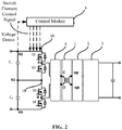
- FIG. 2 is a schematic diagram illustrating another structure of the DC/DC converter using a three-level circuit shown in FIG. 1 .
- the DC/DC converter 100 may further include only a first passive network 4 or a second passive network 5, or may include both the first passive network 4 and the second passive network 5.
- the first passive network 4 is coupled between the fourth node A, the fifth node B, and the primary winding of the transformer 1, and the second passive network 5 is coupled between the secondary winding of the transformer 1 and the secondary side circuit 2.
- a circuit structure of the first passive network and/or the second passive network may include only a capacitor or a network composed of a capacitor and an inductor connected in series, parallel, or series-parallel, and the disclosure is not limited thereto.
- Typical three-level circuits include two structures, a diode neutral point clamp (DNPC) and a series dual half-bridge (SHB).
- DNPC diode neutral point clamp
- SHB series dual half-bridge
- the first bridge arm and the second bridge arm are two half bridges connected in series by four active devices in series, which may be referred to as the series dual half-bridge (SHB) structure.
- the SHB structure is composed of 4 switches, which can output three levels of +2, +1 and 0.
- the series dual half-bridge structure is simple and the system efficiency is high.
- the control signals of the first switch S1 and the second switch S2 are turned on in a complementary manner, and the control signals of the third switch S3 and the fourth switch S4 are turned on in a complementary manner.
- the duty cycle of the control signals of S1 and S3 is greater than 50%, and the duty cycle of the control signals of S2 and S4 is less than 50%.
- the control signals of S1 and S3 are turned on to generate level 1, the primary side current of the transformer is positive, and the current flows into the neutral point (the first node N1) through S1 and S3.
- the control signals of S1 and S3 are turned on to generate level 1, the primary side current of the transformer is negative, and the current flows out of the neutral point (the first node N1) through S1 and S3.
- the neutral point balance can be controlled by adjusting the effective time difference of level 1 between the positive and negative half period.
- Tpf ⁇ Tnf in one switching period, the current flowing out of the neutral point is larger than the current flowing into the neutral point, causing the voltage U dc2 of the lower half capacitor to decrease and the voltage U dc1 of the upper half capacitor to increase, thereby realizing the adjustment of the voltage of the neutral point.
- the positive and negative half period of level 1 are not equal in effective time, the converter's operating mode is asymmetric in one switching period, and the turn-off current of each switch is different, thus it is difficult to ensure that all switches achieve zero voltage switching (ZVS), conduction loss and switching loss are uneven, thereby affecting thermal design. Therefore, the adjustment performance is poor when the neutral point balance is controlled relying on the time difference of level 1.
- ZVS zero voltage switching
- the control method proposed by the present disclosure has stronger neutral point balance adjustment capability, without affecting the realization of the converter's zero voltage switching (ZVS), the method can balance the switching loss and the conduction loss of the switches, and is applicable to various types of resonant or non-resonant, unidirectional or bidirectional DC/DC circuits with a primary side having a series dual half-bridge three-level structure.
- ZVS zero voltage switching
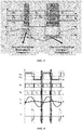
- FIG. 4 is a schematic diagram illustrating a control method provided by the present disclosure. The control method shown in FIG. 4 can be applied to the circuits shown in FIGS. 1 and 2 .
- Ugs is the control signal level of respective switch
- i Lr is the current flowing through the secondary side
- i m is the excitation current of transformer 1
- i N is the current at the first node, that is, the neutral point current.
- the gray part in the drawing is the first phase shift angle.
- the control signals of the first switch S1 and the second switch S2 are turned on in a complementary manner, and the control signals of the third switch S3 and the fourth switch S4 are turned on in a complementary manner.
- the duty cycle of all switch control signals is 50%.
- this method is referred to as a phase-shift modulation method.
- the first phase shift angle will be taken as an example, referring to FIGs. 5A to 5D .
- level 0 and level 2 have no effect on the voltage of the neutral point.
- the converter itself does not have the ability to adjust the neutral point. Therefore, when the neutral point balance adjustment is required, the level 1 mode must be used reasonably to adjust the voltage of the neutral point.
- the series dual half-bridge three-level bridge arm undergoes two level 1 modes in one switching period.
- the first phase shift angle is positive
- the current is always in a direction of flowing out of the neutral point
- the upper half capacitor C 1 is charged
- the lower half capacitor C 2 is discharged, thereby causing the voltage of the neutral point to fall and the voltage difference between the two capacitors to decrease.
- the phase shift angle is negative
- the current is always in a direction of flowing into the neutral point
- the lower half capacitor C 1 is charged, and the upper half capacitor C 2 is discharged, thereby causing the voltage of the neutral point to rise and the voltage difference between the two capacitors to decrease.
- the direction of the current flowing through the neutral point depends on the phase shift angle between the control signals of the two bridge arms.
- the larger the phase shift angle the longer the time on which the level 1 acts, the longer the time on which the current flows through the neutral point, the higher the average current value of the neutral point, and the stronger the adjustment capability.
- the controller 3 of the DC/DC converter may include:
- the phase difference determining unit 32 may be, for example, a regulator.
- the control signal output unit 33 receives an input of a first phase shift angle determined by the regulator and a switching frequency, so as to generate and output the first control signal to the fourth control signal.
- the DC/DC converter control method based on phase shift modulation proposed by embodiments of the present disclosure has at least the following advantages.
- FIG. 8 is a schematic diagram illustrating a passive network structure in an embodiment of the present disclosure.
- the first passive network 4 may include: a resonant capacitor C L , coupled to the fourth node A and connected in series with the primary winding of the transformer 1 through the sixth node C, or coupled to the fifth node B and connected in series with the primary winding of the transformer 1 through the seventh node D.
- the resonance capacitor C L may form a resonance circuit with an excitation inductance and a leakage inductance of the transformer 1.
- the primary winding of the transformer 1 is electrically connected to the series dual half-bridge three-level circuit (including the first capacitor C 1 , the second capacitor C 2 , the first bridge arm 1A, and the second bridge arm 1B) through the first passive network 4.
- the first passive network 4 may only include a resonance capacitor, and form a resonance network with the excitation inductance and leakage inductance of the transformer 1.
- the control method shown in FIG. 4 can be applied to adjust the voltage of the neutral point of the series dual half-bridge three-level circuit.
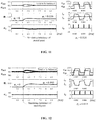
- FIG. 9 is a simulation waveform when the control method is applied to the circuit shown in FIG. 8 .
- the simulation conditions are that frequency modulation control is applied to the LLC voltage conversion circuit, and the output voltage Uo is set to a constant voltage.
- the neutral point imbalance was simulated, the voltages of the two input capacitors are set in such a way that the first voltage U dcP rises and the second voltage U dcN falls.
- the control method shown in FIG. 4 is applied to determine the polarity (positive or negative) and amplitude of the first phase shift angle ⁇ x, and the first phase shift angle is adjusted according to the voltage difference between the two input capacitors.
- the first phase shift angle ⁇ x increases, and the duration of the level 1 mode increases, so the neutral point current i N increases during the level 1 mode, the neutral point voltage decreases, and the voltages of the two input capacitors tend to be balance again.
- the first passive network 4 may also be a series resonant network or a parallel resonant network, and may include an inductor and a capacitor.
- FIG. 10 is a schematic diagram illustrating another passive network structure 4 according to an embodiment of the present disclosure.
- the first passive network 4 may include: a DC blocking capacitor C B , coupled to the fourth node A and connected in series with the primary winding of the transformer 1 through the sixth node C, or coupled to the fifth node B and connected in series with the primary winding of the transformer 1 through the seventh node D.
- the capacitance of the DC-blocking capacitor C B is large and does not resonate with the excitation inductance and leakage inductance of the transformer 1.
- the primary side circuit of the transformer is a DAB circuit of a series dual half-bridge circuit.
- the magnitude and direction of the output power can be controlled by adjusting the phase shift angle between the primary side switch signal and the secondary side switch signal.
- modulation of the secondary side circuit lags the primary side circuit, the power flows in a forward direction (from the left side of the transformer to the right side of the transformer); when modulation of the secondary side circuit is ahead of the primary side circuit, the power flows in a reverse direction.
- FIG. 11 is a simulation waveform when the control method is applied to the circuit shown in FIG. 10 with a power flow in a forward direction.
- the DAB circuit runs in a forward direction.
- the neutral point imbalance was simulated.
- the voltages of the two input capacitors are set in such a way that the first voltage U dcP rises and the second voltage U dcN falls.
- the control method shown in FIG. 4 is applied to determine the polarity (positive or negative) and the amplitude of the first phase shift angle ⁇ x, and the first phase shift angle ⁇ x is increased according to the voltage difference between the two input capacitors, thereby increasing the duration of the level 1 mode. So, the neutral point current i N increases during the level 1 mode, the neutral point voltage decreases and, after a period of time, the voltages of the two input capacitors tend to be balance again.
- FIG. 12 is a simulation waveform when the control method is applied to the circuit shown in FIG. 10 with a power flow in a reverse direction.
- the DAB circuit when u CD is ahead of u AB , the DAB circuit operates in a reverse direction. Similarly, the control method shown in FIG. 4 can be applied to achieve the voltage balance control of the input capacitor.
- the neutral point balance control method (controlling voltage balance of the input capacitors) provided by the embodiments of the present disclosure can be applied to a voltage conversion circuit in which the secondary side circuit 2 of the transformer has various forms.
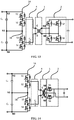
- FIG. 13 is a schematic diagram illustrating a structure of the secondary side circuit 2.
- the secondary side circuit 2 may be a full-bridge rectification circuit, including:
- the fifth switch S5 and the seventh switch S7 are coupled to the tenth node N10, the sixth switch S6 and the eighth element S8 are coupled to the eleventh node N11, and the secondary side circuit 2 is electrically connected to the secondary winding of the transformer 1 through the eighth node N8 and the ninth node N9.
- the eighth node N8 and the ninth node N9 may be directly coupled to the secondary winding of the transformer 1, or may be electrically connected to the secondary winding of the transformer 1 through the second passive network 5.
- the circuit form of the second passive network 5 may be the same as or different from that of the first passive network 4, and is not limited by the disclosure.
- the primary side circuit of the transformer is a series dual half-bridge circuit, and the control method shown in FIG. 4 can be applied to adjust balance of the voltage of the neutral point in the primary side circuit.
- the output ports of the two bridge arms 1A and 1B are connected to the primary winding of the transformer 1 through the first passive network 4 (the structure of the first passive network 4 is not limited), and the secondary side circuit 2 is a full-bridge rectification circuit.
- FIG. 14 is a schematic diagram illustrating another circuit structure of the secondary side circuit 2.
- the secondary side circuit 2 of the transformer may be a full-wave rectification circuit, including:
- the primary side circuit of the transformer is a series dual half-bridge circuit, and the phase shift modulation method shown based on FIG. 4 can be applied to adjust balance of the voltage of the neutral point.
- the output ports of the two bridge arms 1A and 1B are connected to the primary winding of the transformer 1 through the first passive network 4 (the structure of the passive network is not limited), and the secondary side circuit 2 is a full-wave rectification circuit.
- the secondary side circuit 2 is a rectification circuit as shown above, uncontrolled rectification or synchronous rectification, or other modulation methods may be applied to the secondary side circuit 2.
- FIG. 15 is a schematic diagram illustrating yet another circuit structure of the secondary side circuit 2.
- the secondary side circuit 2 may also be a series dual half-bridge (SHB) structure, including:
- control method may further include:
- controlling the second phase shift angle to reduce a voltage difference between the third capacitor and the fourth capacitor includes:
- the neutral point balance of the secondary side circuit 2 can also be adjusted in the manner shown in FIG. 4 , which is not repeated in this disclosure.
- the voltage input source may also be coupled to the secondary side circuit 2.
- the circuit may run in the forward or reverse direction, or in bidirectional operation, which is not specifically limited in this disclosure.
- the above described passive network structure of the DC/DC converter using the three-level circuit and the structure of the secondary side circuit of the transformer are merely examples.
- the above examples may be combined with each other, and other structures may also be included in other embodiments, as long as the primary side circuit of the transformer is provided with the three-level circuit in SHB structure, the control method provided by the present disclosure can be applied to adjust the voltage of the neutral point.
- the first switch and the second switch are turned on in a complementary manner
- the third switch and the fourth switch are turned on in a complementary manner, causing a phase shift angle between control signals of the first switch and the fourth switch, and adjusting the phase shift angle to reduce a voltage difference between the first capacitor and the second capacitor, thereby effectively adjusting balance of the voltage of the neutral point for the DC/DC converter.
- the working modes of the positive and negative half periods are completely symmetrical, the effect on the neutral point is the same, and the on-times of the switches in the SHB structure are the same.
- the method according to the embodiments of the present disclosure has a higher neutral point adjustment capability, which is beneficial for all the four switches in the bridge arm to realize ZVS and, at the same time, causes the stresses and losses of the four switches to be uniform, thereby improving energy efficiency.
- modules or units of the device for action execution are mentioned in the detailed description above, this division is not mandatory.
- the features and functions of two or more modules or units described above may be embodied in one module or unit.
- the features and functions of a module or unit described above can be further divided into multiple modules or units to be embodied.
Landscapes
- Engineering & Computer Science (AREA)
- Power Engineering (AREA)
- Dc-Dc Converters (AREA)
Abstract
Description
- The present disclosure relates to the field of power supply technology, and in particular, to a control method of a DC/DC converter and the DC/DC converter as involved.
- High-voltage DC/DC converters are widely used in high-power DC conversion systems, new energy storage systems, electric vehicle charging devices, rail transit power distribution systems, and the like. In order to reduce wire losses and costs, increase voltage levels, and reduce the number of cascade units, high-voltage DC/DC converter usually realizes high-voltage input by means of a three-level circuit. Affected by factors such as inconsistent hardware parameters, the voltage of the neutral point of the three-level circuit may appear unbalanced, which affects the safety of the device and the normal operation of the converter. Thus, the voltage of the neutral point must be subject to balance control.
- Therefore, a need exists for a control method of a DC/DC converter capable of performing adjustment on the voltage of the neutral point (neutral point balance) of the DC / DC converter.
- It should be noted that the information disclosed in the background section above is only used to enhance the understanding of the background of the disclosure, and therefore may include information that does not constitute the prior art known to those of ordinary skill in the art.
- The present disclosure is directed to provide a control method of a DC/DC converter and a control device of the DC/DC converter, thereby adjusting balance of the voltage of the neutral point for the DC/DC converter.
- According to a first aspect of the disclosure, there is provided a control method of a DC/DC converter, applied to a DC/DC converter, the DC/DC converter including: a first capacitor and a second capacitor coupled to a first node, a second end of the first capacitor being coupled to a second node, and a second end of the second capacitor being coupled to a third node; a first bridge arm coupled between the first node and the second node and a second bridge arm coupled between the first node and the third node, the first bridge arm including a first switch and a second switch coupled to a fourth node, the second bridge arm including a third switch and a fourth switch coupled to a fifth node; a transformer having a primary winding electrically connected to the fourth node and the fifth node, and a secondary side circuit electrically connected to a secondary winding of the transformer, wherein the method includes:
- outputting a first control signal, a second control signal, a third control signal, and a fourth control signal to control ends of the first switch, the second switch, the third switch, and the fourth switch, wherein the first control signal, the second control signal, the third control signal, and the fourth control signal are square wave signals having a preset period, the first control signal is complementary to the second control signal, the third control signal is complementary to the fourth control signal, a first phase shift angle exists between the first control signal and the fourth control signal, and the first phase shift angle exists between the second control signal and the third control signal; and
- controlling the first phase shift angle to reduce a voltage difference between the first capacitor and the second capacitor.
- According to a second aspect of the disclosure, there is provided a DC/DC converter, including:
- a first capacitor, having a first end coupled to a first node and a second end coupled to a second node;
- a second capacitor, having a first end coupled to the first node and a second end coupled to a third node;
- a first bridge arm, coupled between the first node and the second node, including a first switch and a second switch coupled to a fourth node;
- a second bridge arm, coupled between the first node and the third node, including a third switch and a fourth switch coupled to a fifth node;
- a transformer, having a primary winding electrically connected to the fourth node and the fifth node;
- a secondary side circuit, electrically connected to a secondary winding of the transformer;
- a processor, coupled to the first capacitor, the second capacitor, the first bridge arm, the second bridge arm and the secondary side circuit, and configured to:
- output a first control signal, a second control signal, a third control signal, and a fourth control signal to control ends of the first switch, the second switch, the third switch, and the fourth switch, wherein the first control signal, the second control signal, the third control signal, and the fourth control signal are square wave signals having a preset period, the first control signal is complementary to the second control signal, the third control signal is complementary to the fourth control signal, a first phase shift angle exists between the first control signal and the fourth control signal, and the first phase shift angle exists between the second control signal and the third control signal; and
- control the first phase shift angle to reduce a voltage difference between the first capacitor and the second capacitor.
- It should be understood that the above general description and the following detailed description are merely exemplary and explanatory, and should not limit the present disclosure.
- The accompanying drawings herein are incorporated in and constitute a part of this specification, illustrate embodiments conforming to the present disclosure and together with the description serve to explain the principles of the present disclosure. Apparently, the accompanying drawings in the following description show merely some embodiments of the present disclosure, and persons of ordinary skill in the art may still derive other drawings from these accompanying drawings without creative efforts.
-
FIG. 1 is a schematic diagram illustrating a DC/DC converter using a three-level circuit. -
FIG. 2 is a schematic diagram illustrating another structure of the DC/DC converter using a three-level circuit shown inFIG. 1 . -
FIG. 3 is a schematic diagram illustrating a method of neutral point balance in the related art. -
FIG. 4 is a schematic diagram illustrating a control method provided by the present disclosure. -
FIGs. 5A-5D are schematic diagrams illustrating four switching modes of a series dual half-bridge three-level circuit. -
FIG. 6 is a block diagram illustrating a processor of the DC / DC converter provided by the present disclosure. -
FIG. 7 is a schematic diagram illustrating signal relationships of the processor inFIG. 6 . -
FIG. 8 is a schematic diagram illustrating a passive network structure according to an embodiment of the present disclosure. -
FIG. 9 is a simulation waveform when the control method is applied to the circuit shown inFIG. 8 . -
FIG. 10 is a schematic diagram illustrating another passive network structure according to an embodiment of the present disclosure. -
FIG. 11 is a simulation waveform when the control method is applied to the circuit shown inFIG. 10 with a power flow in a forward direction. -
FIG. 12 is a simulation waveform when the control method is applied to the circuit shown inFIG. 10 with a power flow in a reverse direction. -
FIG. 13 is a schematic diagram illustrating a secondary side circuit having a full-bridge structure. -
FIG. 14 is a schematic diagram illustrating a secondary side circuit having a full-wave rectification structure. -
FIG. 15 is a schematic diagram illustrating a secondary side circuit having a series dual half-bridge structure. - Exemplary embodiments will be described more comprehensively by referring to accompanying drawings now. However, the exemplary embodiments can be embodied in many forms and should not be construed as limited to the embodiments set forth herein; rather, these embodiments are provided so that this disclosure will be made thorough and complete, and the concept of exemplary embodiments will be fully conveyed to those skilled in the art. Furthermore, the described features, structures, or characteristics may be combined in any suitable manner in one or more embodiments. In the following description, numerous specific details are provided to provide a thorough understanding of the embodiments of the present disclosure. Those skilled in the art will recognize, however, that the technical solution of the present disclosure may be practiced without one or more of the specific details described, or that other methods, components, materials, etc. may be employed. In other instances, well-known technical solutions are not shown or described in detail to avoid obscuring aspects of the present disclosure.
- Furthermore, the accompanying drawings are merely schematic illustrations of the present disclosure. Same or similar parts are denoted by same reference numbers in the drawings and, thus, a detailed description thereof will be omitted. Some block diagrams shown in the figures are functional entities and not necessarily to be corresponding to a physically or logically individual entities. These functional entities may be implemented in software form, or implemented in one or more hardware modules or integrated circuits, or implemented in different networks and/or processor apparatuses and/or microcontroller apparatuses.
- A detailed description of the exemplary embodiments of the present disclosure will be made in the following with reference to the accompanying drawings.
-
FIG. 1 is a schematic diagram illustrating a DC/DC converter using a three-level circuit. - Referring to
FIG. 1 , the DC/DC converter 100 may include: - a first capacitor C1, having a first end coupled to a first node N1, and a second end coupled to a second node N2;
- a second capacitor C2, having a first end coupled to the first node N1, and a second end coupled to a third node N3;
- a
first bridge arm 1A, coupled between the first node N1 and the second node N2, and including a first switch S1 and a second switch S2 connected in series, the first switch S1 and the second switch S2 being coupled to a fourth node A; - a
second bridge arm 1B, coupled between the first node N1 and the third node N3, and including a third switch S3 and a fourth switch S4 connected in series, the third switch S3 and the fourth switch S4 being coupled to a fifth node B; - a
transformer 1, having a primary winding electrically connected to the fourth node A and the fifth node B, respectively, through a sixth node C and a seventh node D; - a
secondary side circuit 2, electrically connected to a secondary winding of thetransformer 1 through an eighth node N8 and a ninth node N9; - a
processor 3, coupled to the first capacitor C1, the second capacitor C2, thefirst bridge arm 1A, thesecond bridge arm 1B and thesecondary side circuit 2, and configured to output a first control signal, a second control signal, a third control signal, and a fourth control signal to control ends of the first switch S1, the second switch S2, the third switch S3, and the fourth switch S4, wherein the first control signal, the second control signal, the third control signal, and the fourth control signal are square wave signals having a preset period, the first control signal is complementary to the second control signal, the third control signal is complementary to the fourth control signal, a first phase shift angle exists between the first control signal and the fourth control signal, and the first phase shift angle exists between the second control signal and the third control signal; and control the first phase shift angle to reduce a voltage difference between the first capacitor and the second capacitor. -
FIG. 2 is a schematic diagram illustrating another structure of the DC/DC converter using a three-level circuit shown inFIG. 1 . - Referring to
FIG. 2 , the DC/DC converter 100 may further include only a firstpassive network 4 or a secondpassive network 5, or may include both the firstpassive network 4 and the secondpassive network 5. The firstpassive network 4 is coupled between the fourth node A, the fifth node B, and the primary winding of thetransformer 1, and the secondpassive network 5 is coupled between the secondary winding of thetransformer 1 and thesecondary side circuit 2. A circuit structure of the first passive network and/or the second passive network may include only a capacitor or a network composed of a capacitor and an inductor connected in series, parallel, or series-parallel, and the disclosure is not limited thereto. - Typical three-level circuits include two structures, a diode neutral point clamp (DNPC) and a series dual half-bridge (SHB). In
FIG. 1 andFIG. 2 , the first bridge arm and the second bridge arm are two half bridges connected in series by four active devices in series, which may be referred to as the series dual half-bridge (SHB) structure. The SHB structure is composed of 4 switches, which can output three levels of +2, +1 and 0. For DC/DC converters, the series dual half-bridge structure is simple and the system efficiency is high. - In order to solve the problem of the neutral point balance control of a three-level circuit, there is proposed a neutral point control method based on duty cycle modulation in related art. As shown in
FIG. 3 , the control signals of the first switch S1 and the second switch S2 are turned on in a complementary manner, and the control signals of the third switch S3 and the fourth switch S4 are turned on in a complementary manner. The duty cycle of the control signals of S1 and S3 is greater than 50%, and the duty cycle of the control signals of S2 and S4 is less than 50%. During the period of t1-t2, the control signals of S1 and S3 are turned on to generatelevel 1, the primary side current of the transformer is positive, and the current flows into the neutral point (the first node N1) through S1 and S3. During the period of t6-t7, the control signals of S1 and S3 are turned on to generatelevel 1, the primary side current of the transformer is negative, and the current flows out of the neutral point (the first node N1) through S1 and S3. In a switching period, the two level-1 states have opposite effects on the neutral point, so the neutral point balance can be controlled by adjusting the effective time difference oflevel 1 between the positive and negative half period. When Tpf<Tnf, in one switching period, the current flowing out of the neutral point is larger than the current flowing into the neutral point, causing the voltage Udc2 of the lower half capacitor to decrease and the voltage Udc1 of the upper half capacitor to increase, thereby realizing the adjustment of the voltage of the neutral point. - In this control method, the positive and negative half period of
level 1 are not equal in effective time, the converter's operating mode is asymmetric in one switching period, and the turn-off current of each switch is different, thus it is difficult to ensure that all switches achieve zero voltage switching (ZVS), conduction loss and switching loss are uneven, thereby affecting thermal design. Therefore, the adjustment performance is poor when the neutral point balance is controlled relying on the time difference oflevel 1. - In view of the problems in the related art, the control method proposed by the present disclosure has stronger neutral point balance adjustment capability, without affecting the realization of the converter's zero voltage switching (ZVS), the method can balance the switching loss and the conduction loss of the switches, and is applicable to various types of resonant or non-resonant, unidirectional or bidirectional DC/DC circuits with a primary side having a series dual half-bridge three-level structure.
-
FIG. 4 is a schematic diagram illustrating a control method provided by the present disclosure. The control method shown inFIG. 4 can be applied to the circuits shown inFIGS. 1 and2 . - In
Fig. 4 , Ugs is the control signal level of respective switch, iLr is the current flowing through the secondary side, im is the excitation current oftransformer 1, and iN is the current at the first node, that is, the neutral point current. The gray part in the drawing is the first phase shift angle. - Referring to
FIG. 4 , in the embodiment of the present disclosure, it is controlled in such a way that the control signals of the first switch S1 and the second switch S2 are turned on in a complementary manner, and the control signals of the third switch S3 and the fourth switch S4 are turned on in a complementary manner. Ideally, ignoring the dead zone, the duty cycle of all switch control signals is 50%. There is a first phase shift angle ϕx between the control signals of the switches S1 and S2 of thefirst bridge arm 1A and the control signals of the switches S3 and S4 of thesecond bridge arm 1B. It is defined that the phase shift angle is positive when conduction of S4 lag conduction of S1, and the phase shift angle is negative when conduction of S4 is ahead of conduction of S1. In the embodiments of the present disclosure, this method is referred to as a phase-shift modulation method. - Regardless of the dead time, four working modes may be formed by the series dual half-bridge three-level bridge arm in one switching period. The first phase shift angle will be taken as an example, referring to
FIGs. 5A to 5D . - In
FIG. 5A , when S1 and S4 are turned on at the same time, two input capacitors C1 and C2 are connected in series to the converter. The total output voltage of the first bridge arm and the second bridge arm is (Udc1 + Udc2) and the output level is 2. The neutral point (first node N1) is not connected to the circuit and, thus the voltage of the neutral point would not be affected in this mode. - In
FIG. 5B , when S2 and S3 are turned on at the same time, the two input capacitors C1 and C2 are not connected to the converter. The total output voltage of thefirst bridge arm 1A and thesecond bridge arm 1B is 0, and the output level is 0. The neutral point (first node N1) is not connected to the circuit and, thus the voltage of the neutral point would not be affected in this mode. - In
FIG. 5C , when S1 and S3 are turned on at the same time, the total output voltage of thefirst bridge arm 1A and thesecond bridge arm 1B is Udc1, the output level is 1. The neutral point (first node N1) is connected to the circuit, and the primary side current of the converter flows out of the neutral point through the two switches S1 and S3. - In
FIG. 5D , when S2 and S4 are turned on at the same time, the total output voltage of thefirst bridge arm 1A and thesecond bridge arm 1B is Udc2, the output level is 1. The neutral point (first node N1) is connected to the circuit, and the primary side current of the converter flows out of the midpoint through the two switches S2 and S4. - In the above four switching modes,
level 0 andlevel 2 have no effect on the voltage of the neutral point. When the primary side circuit works in the 0/2 two-level modulation mode, the converter itself does not have the ability to adjust the neutral point. Therefore, when the neutral point balance adjustment is required, thelevel 1 mode must be used reasonably to adjust the voltage of the neutral point. - In the control method shown in
FIG. 4 , the series dual half-bridge three-level bridge arm undergoes twolevel 1 modes in one switching period. When the first phase shift angle is positive, the current is always in a direction of flowing out of the neutral point, the upper half capacitor C1 is charged, and the lower half capacitor C2 is discharged, thereby causing the voltage of the neutral point to fall and the voltage difference between the two capacitors to decrease. When the phase shift angle is negative, the current is always in a direction of flowing into the neutral point, the lower half capacitor C1 is charged, and the upper half capacitor C2 is discharged, thereby causing the voltage of the neutral point to rise and the voltage difference between the two capacitors to decrease. - Therefore, the direction of the current flowing through the neutral point depends on the phase shift angle between the control signals of the two bridge arms. The larger the phase shift angle, the longer the time on which the
level 1 acts, the longer the time on which the current flows through the neutral point, the higher the average current value of the neutral point, and the stronger the adjustment capability. - Referring to
FIG. 6 , in an embodiment of the present disclosure, thecontroller 3 of the DC/DC converter may include: - a
voltage detection unit 31, configured to detect a first voltage across the first capacitor and a second voltage across the second capacitor; - a phase
difference determining unit 32, configured to determine the first phase shift angle according to the difference between the first voltage and the second voltage, reduce the first phase shift angle when the difference is a positive value, and increase the first phase shift angle when the difference is a negative value; - a control
signal output unit 33, configured to output a first control signal, a second control signal, a third control signal, and a fourth control signal according to the first phase shift angle, so as to control the on and off of the first to fourth switches S1 to S4. - Referring to
FIG. 7 , in the embodiment of the present disclosure, the phasedifference determining unit 32 may be, for example, a regulator. The controlsignal output unit 33 receives an input of a first phase shift angle determined by the regulator and a switching frequency, so as to generate and output the first control signal to the fourth control signal. - Compared with related art, the DC/DC converter control method based on phase shift modulation proposed by embodiments of the present disclosure has at least the following advantages.
- 1. The working modes of the positive and negative half control periods are completely symmetrical, the positive and negative half control periods have the same effect on the neutral point and, through superposition, may obtain a stronger adjustment ability. 2. The current at the primary side circuit of the transformer is symmetrical, which is beneficial for the switches in the primary side circuit to achieve ZVS. 3. The stress and loss of the four switches in the primary side circuit may be made uniform, thereby improving energy efficiency.
-
FIG. 8 is a schematic diagram illustrating a passive network structure in an embodiment of the present disclosure. - Referring to
FIG. 8 , in one embodiment, the firstpassive network 4 may include:
a resonant capacitor CL, coupled to the fourth node A and connected in series with the primary winding of thetransformer 1 through the sixth node C, or coupled to the fifth node B and connected in series with the primary winding of thetransformer 1 through the seventh node D. The resonance capacitor CL may form a resonance circuit with an excitation inductance and a leakage inductance of thetransformer 1. - In the embodiment shown in
FIG. 8 , the primary winding of thetransformer 1 is electrically connected to the series dual half-bridge three-level circuit (including the first capacitor C1, the second capacitor C2, thefirst bridge arm 1A, and thesecond bridge arm 1B) through the firstpassive network 4. The firstpassive network 4 may only include a resonance capacitor, and form a resonance network with the excitation inductance and leakage inductance of thetransformer 1. At this time, no matter what kind of circuit form thesecondary side circuit 2 is, the control method shown inFIG. 4 can be applied to adjust the voltage of the neutral point of the series dual half-bridge three-level circuit. -
FIG. 9 is a simulation waveform when the control method is applied to the circuit shown inFIG. 8 . - Referring to
FIG. 9 , the simulation conditions are that frequency modulation control is applied to the LLC voltage conversion circuit, and the output voltage Uo is set to a constant voltage. At a time point of 6 ms, the neutral point imbalance was simulated, the voltages of the two input capacitors are set in such a way that the first voltage UdcP rises and the second voltage UdcN falls. The control method shown inFIG. 4 is applied to determine the polarity (positive or negative) and amplitude of the first phase shift angle ϕx, and the first phase shift angle is adjusted according to the voltage difference between the two input capacitors. After a period of time, the first phase shift angle ϕx increases, and the duration of thelevel 1 mode increases, so the neutral point current iN increases during thelevel 1 mode, the neutral point voltage decreases, and the voltages of the two input capacitors tend to be balance again. - In other embodiments, the first
passive network 4 may also be a series resonant network or a parallel resonant network, and may include an inductor and a capacitor. -
FIG. 10 is a schematic diagram illustrating anotherpassive network structure 4 according to an embodiment of the present disclosure. - Referring to
FIG. 10 , in another embodiment, the firstpassive network 4 may include:
a DC blocking capacitor CB, coupled to the fourth node A and connected in series with the primary winding of thetransformer 1 through the sixth node C, or coupled to the fifth node B and connected in series with the primary winding of thetransformer 1 through the seventh node D. The capacitance of the DC-blocking capacitor CB is large and does not resonate with the excitation inductance and leakage inductance of thetransformer 1. - In the embodiment shown in
FIG. 10 , the primary side circuit of the transformer is a DAB circuit of a series dual half-bridge circuit. At this time, the magnitude and direction of the output power can be controlled by adjusting the phase shift angle between the primary side switch signal and the secondary side switch signal. When modulation of the secondary side circuit lags the primary side circuit, the power flows in a forward direction (from the left side of the transformer to the right side of the transformer); when modulation of the secondary side circuit is ahead of the primary side circuit, the power flows in a reverse direction. -
FIG. 11 is a simulation waveform when the control method is applied to the circuit shown inFIG. 10 with a power flow in a forward direction. - Referring to
FIG. 11 , when uCD lags behind uAB, the DAB circuit runs in a forward direction. At a time point of 6 ms, the neutral point imbalance was simulated. The voltages of the two input capacitors are set in such a way that the first voltage UdcP rises and the second voltage UdcN falls. The control method shown inFIG. 4 is applied to determine the polarity (positive or negative) and the amplitude of the first phase shift angle ϕx, and the first phase shift angle ϕx is increased according to the voltage difference between the two input capacitors, thereby increasing the duration of thelevel 1 mode. So, the neutral point current iN increases during thelevel 1 mode, the neutral point voltage decreases and, after a period of time, the voltages of the two input capacitors tend to be balance again. -
FIG. 12 is a simulation waveform when the control method is applied to the circuit shown inFIG. 10 with a power flow in a reverse direction. - Referring to
FIG. 12 , when uCD is ahead of uAB, the DAB circuit operates in a reverse direction. Similarly, the control method shown inFIG. 4 can be applied to achieve the voltage balance control of the input capacitor. - The neutral point balance control method (controlling voltage balance of the input capacitors) provided by the embodiments of the present disclosure can be applied to a voltage conversion circuit in which the
secondary side circuit 2 of the transformer has various forms. -
FIG. 13 is a schematic diagram illustrating a structure of thesecondary side circuit 2. - Referring to
FIG. 13 , thesecondary side circuit 2 may be a full-bridge rectification circuit, including: - a
fourth bridge arm 2A, including a fifth switch S5 and a sixth switch S6 coupled to the eighth node N8; and - a
fifth bridge arm 2B, including a seventh switch S7 and an eighth switch S8 coupled to the ninth node N9. - The fifth switch S5 and the seventh switch S7 are coupled to the tenth node N10, the sixth switch S6 and the eighth element S8 are coupled to the eleventh node N11, and the
secondary side circuit 2 is electrically connected to the secondary winding of thetransformer 1 through the eighth node N8 and the ninth node N9. - In some embodiments, the eighth node N8 and the ninth node N9 may be directly coupled to the secondary winding of the
transformer 1, or may be electrically connected to the secondary winding of thetransformer 1 through the secondpassive network 5. The circuit form of the secondpassive network 5 may be the same as or different from that of the firstpassive network 4, and is not limited by the disclosure. - In the embodiment shown in
FIG. 13 , the primary side circuit of the transformer is a series dual half-bridge circuit, and the control method shown inFIG. 4 can be applied to adjust balance of the voltage of the neutral point in the primary side circuit. The output ports of the twobridge arms transformer 1 through the first passive network 4 (the structure of the firstpassive network 4 is not limited), and thesecondary side circuit 2 is a full-bridge rectification circuit. -
FIG. 14 is a schematic diagram illustrating another circuit structure of thesecondary side circuit 2. - Referring to
FIG. 14 , thesecondary side circuit 2 of the transformer may be a full-wave rectification circuit, including: - a fifth switch S5, having a first end electrically connected to one end of the secondary winding of the
transformer 1 through the eighth node N8; and - a sixth switch S6, having a first end electrically connected to the other end of the secondary winding of the
transformer 1 through the ninth node N9, and a second end coupled to a second end of the fifth switch S5. - In the embodiment shown in
FIG. 14 , the primary side circuit of the transformer is a series dual half-bridge circuit, and the phase shift modulation method shown based onFIG. 4 can be applied to adjust balance of the voltage of the neutral point. The output ports of the twobridge arms transformer 1 through the first passive network 4 (the structure of the passive network is not limited), and thesecondary side circuit 2 is a full-wave rectification circuit. - In this embodiment, when the
secondary side circuit 2 is a rectification circuit as shown above, uncontrolled rectification or synchronous rectification, or other modulation methods may be applied to thesecondary side circuit 2. -
FIG. 15 is a schematic diagram illustrating yet another circuit structure of thesecondary side circuit 2. - Referring to
FIG. 15 , in an embodiment, thesecondary side circuit 2 may also be a series dual half-bridge (SHB) structure, including: - a third capacitor C3 and a fourth capacitor C4 coupled to a tenth node N10, a second end of the third capacitor C3 being coupled to an eleventh node N11, and a second end of the fourth capacitor C4 being coupled to a twelfth node N12; and
- a
third bridge arm 2A coupled between the tenth node N10 and the eleventh node N11, and afourth bridge arm 2B coupled between the twelfth node N12 and the tenth node N10. Thethird bridge arm 2A includes a fifth switch S5 and a sixth switch S6 coupled to a thirteenth node N13. Thefourth bridge arm 2B includes a seventh switch S7 and an eighth switch S8 coupled to a fourteenth node N14. Thesecondary side circuit 2 is electrically connected to the secondary winding of thetransformer 1 through the thirteenth node N13 and the fourteenth node N14. - In the embodiment shown in
FIG. 15 , the control method may further include: - outputting a fifth control signal, a sixth control signal, a seventh control signal, and an eighth control signal to control ends of the fifth switch, the sixth switch, the seventh switch and the eighth switch, wherein the fifth control signal, the sixth control signal, the seventh control signal, and the eighth control signal are square wave signals having a preset period, the fifth control signal is complementary to the sixth control signal, the seventh control signal is complementary to the eighth control signal, a second phase shift angle exists between the fifth control signal and the eighth control signal, and the second phase shift angle exists between the sixth control signal and the seventh control signal; and
- controlling the second phase shift angle to reduce a voltage difference between the third capacitor and the fourth capacitor.
- In an embodiment, the controlling the second phase shift angle to reduce a voltage difference between the third capacitor and the fourth capacitor includes:
- detecting a third voltage across the third capacitor and a fourth voltage across the fourth capacitor; and
- determining the second phase shift angle according to a difference between the third voltage and the fourth voltage, reducing the second phase shift angle when the difference is a positive value, and increasing the second phase shift angle when the difference is a negative value.
- When the
secondary side circuit 2 has an SHB structure, the neutral point balance of thesecondary side circuit 2 can also be adjusted in the manner shown inFIG. 4 , which is not repeated in this disclosure. - Although the embodiments of the present disclosure are described with an example in which the voltage input source is coupled to the second node and the third node, in other embodiments, the voltage input source may also be coupled to the
secondary side circuit 2. In other words, the circuit may run in the forward or reverse direction, or in bidirectional operation, which is not specifically limited in this disclosure. - The above described passive network structure of the DC/DC converter using the three-level circuit and the structure of the secondary side circuit of the transformer are merely examples. The above examples may be combined with each other, and other structures may also be included in other embodiments, as long as the primary side circuit of the transformer is provided with the three-level circuit in SHB structure, the control method provided by the present disclosure can be applied to adjust the voltage of the neutral point.
- In summary, according to the embodiments of the present disclosure, it is controlled in such a way that, on two bridge arms of the DC/DC converter in SHB structure, the first switch and the second switch are turned on in a complementary manner, the third switch and the fourth switch are turned on in a complementary manner, causing a phase shift angle between control signals of the first switch and the fourth switch, and adjusting the phase shift angle to reduce a voltage difference between the first capacitor and the second capacitor, thereby effectively adjusting balance of the voltage of the neutral point for the DC/DC converter. Based on this control method, the working modes of the positive and negative half periods are completely symmetrical, the effect on the neutral point is the same, and the on-times of the switches in the SHB structure are the same. Compared to the method implemented by controlling time difference of the
level 1 mode to achieve neutral point adjustment, which may cause uneven stress on switches, the method according to the embodiments of the present disclosure has a higher neutral point adjustment capability, which is beneficial for all the four switches in the bridge arm to realize ZVS and, at the same time, causes the stresses and losses of the four switches to be uniform, thereby improving energy efficiency. - It should be noted that although several modules or units of the device for action execution are mentioned in the detailed description above, this division is not mandatory. In fact, according to the embodiments of the present disclosure, the features and functions of two or more modules or units described above may be embodied in one module or unit. Similarly, the features and functions of a module or unit described above can be further divided into multiple modules or units to be embodied.
- In addition, the above-mentioned drawings are merely a schematic description of processes included in a method according to an exemplary embodiment of the present invention, and are not limiting purposes. It is easy to understand that the processes shown in the above drawings do not indicate or limit the chronological order of these processes. In addition, it is also easy to understand that these processes may be, for example, performed synchronously or asynchronously in multiple modules.
- Other embodiments of the present disclosure will be apparent to those skilled in the art from consideration of the specification and practice of the invention disclosed here. This application is intended to cover any variations, uses, or adaptations of the present disclosure following the general principles thereof and including such departures from the present disclosure as come within known or customary practice in the art. It is intended that the specification and embodiments be considered as exemplary only, with a true scope and spirit of the present disclosure being indicated by the claims.
Claims (15)
- A control method of a DC/DC converter (100), the DC/DC converter comprising a first capacitor (C1) and a second capacitor (C2) coupled to a first node (N1), a second end of the first capacitor being coupled to a second node (N2), and a second end of the second capacitor being coupled to a third node (N3); a first bridge arm (1A) coupled between the first node and the second node and a second bridge arm (1B) coupled between the first node and the third node, the first bridge arm comprising a first switch (S1) and a second switch (S2) coupled to a fourth node (A), the second bridge arm comprising a third switch (S3) and a fourth switch (S4) coupled to a fifth node (B); a transformer (1) having a primary winding electrically connected to the fourth node and the fifth node, and a secondary side circuit (2) electrically connected to a secondary winding of the transformer, wherein the method comprises:outputting a first control signal, a second control signal, a third control signal, and a fourth control signal to control ends of the first switch, the second switch, the third switch, and the fourth switch, wherein the first control signal, the second control signal, the third control signal, and the fourth control signal are square wave signals having a preset period, the first control signal is complementary to the second control signal, the third control signal is complementary to the fourth control signal, a first phase shift angle exists between the first control signal and the fourth control signal, and the first phase shift angle exists between the second control signal and the third control signal; andcontrolling the first phase shift angle to reduce a voltage difference between the first capacitor and the second capacitor.
- The control method according to claim 1, wherein the controlling the first phase shift angle to reduce a voltage difference between the first capacitor and the second capacitor comprises:detecting a first voltage across the first capacitor and a second voltage across the second capacitor; anddetermining the first phase shift angle according to a difference between the first voltage and the second voltage, reducing the first phase shift angle when the difference is a positive value, and increasing the first phase shift angle when the difference is a negative value.
- The control method according to claim 1, wherein the DC/DC converter further comprises:
an input source, coupled to the second node and the third node or coupled to the secondary side circuit. - The control method according to any one of claims 1 to 3, wherein the secondary side circuit is a full-bridge rectification circuit or a full-wave rectification circuit.
- The control method according to any one of claims 1 to 3, wherein the secondary side circuit comprises a third capacitor (C3) and a fourth capacitor (C4) coupled to a tenth node (N10), a second end of the third capacitor being coupled to an eleventh node (N11), and a second end of the fourth capacitor being coupled to a twelfth node; a third bridge arm (2A) coupled between the eleventh node and the tenth node and a fourth bridge arm (2B) coupled between the twelfth node (N12) and the tenth node (N10), the third bridge arm comprising a fifth switch (55) and a sixth switch (56) coupled to a thirteenth node (N13), the fourth bridge arm comprising a seventh switch (57) and an eighth switch (58) coupled to a fourteenth node (N14), and the secondary winding being electrically connected to the thirteenth node and the fourteenth node.
- The control method according to claim 5, further comprising:outputting a fifth control signal, a sixth control signal, a seventh control signal, and an eighth control signal to control ends of the fifth switch, the sixth switch, the seventh switch and the eighth switch, wherein the fifth control signal, the sixth control signal, the seventh control signal, and the eighth control signal are square wave signals having a preset period, the fifth control signal is complementary to the sixth control signal, the seventh control signal is complementary to the eighth control signal, a second phase shift angle exists between the fifth control signal and the eighth control signal, and the second phase shift angle exists between the sixth control signal and the seventh control signal; andcontrolling the second phase shift angle to reduce a voltage difference between the third capacitor and the fourth capacitor.
- The control method according to claim 6, wherein the controlling the second phase shift angle to reduce a voltage difference between the third capacitor and the fourth capacitor comprises:detecting a third voltage across the third capacitor and a fourth voltage across the fourth capacitor; anddetermining the second phase shift angle according to a difference between the third voltage and the fourth voltage, reducing the second phase shift angle when the difference is a positive value, and increasing the second phase shift angle when the difference is a negative value.
- ADC/DC converter (100), comprising:a first capacitor (C1), having a first end coupled to a first node (N1) and a second end coupled to a second node (N2);a second capacitor (C2), having a first end coupled to the first node (N1) and a second end coupled to a third node (N3);a first bridge arm (1A), coupled between the first node (N1) and the second node (N2), comprising a first switch (S1) and a second switch (S2) coupled to a fourth node (N4);a second bridge arm (1B), coupled between the first node (N1) and the third node (N3), comprising a third switch (S3) and a fourth switch (S4) coupled to a fifth node;a transformer (1), having a primary winding electrically connected to the fourth node (N4) and the fifth node (N5);a secondary side circuit (2), electrically connected to a secondary winding of the transformer (1); anda processor (3), coupled to the first capacitor (C1), the second capacitor (C2), the first bridge arm (1A), the second bridge arm (1B) and the secondary side circuit (2), and configured to:output a first control signal, a second control signal, a third control signal, and a fourth control signal to control ends of the first switch, the second switch, the third switch, and the fourth switch, wherein the first control signal, the second control signal, the third control signal, and the fourth control signal are square wave signals having a preset period, the first control signal is complementary to the second control signal, the third control signal is complementary to the fourth control signal, a first phase shift angle exists between the first control signal and the fourth control signal, and the first phase shift angle exists between the second control signal and the third control signal; andcontrol the first phase shift angle to reduce a voltage difference between the first capacitor and the second capacitor.
- The DC/DC converter according to claim 8, wherein the processor (3) is configured to:detect a first voltage across the first capacitor and a second voltage across the second capacitor;determine the first phase shift angle according to a difference between the first voltage and the second voltage, reduce the first phase shift angle when the difference is a positive value, and increase the first phase shift angle when the difference is a negative value; andoutput the first control signal, the second control signal, the third control signal, and the fourth control signal according to the first phase shift angle.
- The DC/DC converter according to claim 8, further comprising:
at least one of a first passive network (4) or a second passive network (5), the first passive network (4) being coupled between the fourth node (N4), the fifth node (N5) and the primary winding of the transformer (1), the second passive network (5) being coupled between the secondary winding of the transformer (1) and the secondary side circuit (2). - The DC/DC converter according to claim 8, wherein the DC/DC converter further comprises:
an input source, coupled to the second node (N2) and the third node (N3) or coupled to the secondary side circuit (2). - The DC/DC converter according to any one of claims 8 to 11, wherein the secondary side circuit (2) is a full-bridge rectification circuit or a full-wave rectification circuit.
- The DC/DC converter according to any one of claims 8 to 11, wherein the secondary side circuit comprises a third capacitor (C3) and a fourth capacitor (C4) coupled to a tenth node (N10), a second end of the third capacitor (C3) being coupled to an eleventh node (N11), and a second end of the fourth capacitor (C4) being coupled to a twelfth node (N12); a third bridge arm (2A) coupled between the eleventh node (N11) and the tenth node (N10) and a fourth bridge arm (2B) coupled between the twelfth node (N12) and the tenth node (N10), the third bridge arm (2A) comprising a fifth switch (55) and a sixth switch (56) coupled to a thirteenth node (N13), the fourth bridge arm (2B) comprising a seventh switch (57) and an eighth switch (58) coupled to a fourteenth node (N14), and the secondary winding being electrically connected to the thirteenth node (N13) and the fourteenth node (N14).
- The DC/DC converter according to claim 13, wherein the processor (3) is further configured to:output a fifth control signal, a sixth control signal, a seventh control signal, and an eighth control signal are output to control ends of the fifth switch, the sixth switch, the seventh switch and the eighth switch, wherein the fifth control signal, the sixth control signal, the seventh control signal, and the eighth control signal are square wave signals having a preset period, the fifth control signal is complementary to the sixth control signal, the seventh control signal is complementary to the eighth control signal, a second phase shift angle exists between the fifth control signal and the eighth control signal, and the second phase shift angle exists between the sixth control signal and the seventh control signal; andcontrol the second phase shift angle to reduce a voltage difference between the third capacitor and the fourth capacitor.
- The DC/DC converter according to claim 14, wherein the processor (3) is further configured to:detect a third voltage across the third capacitor and a fourth voltage across the fourth capacitor; anddetermine the second phase shift angle according to a difference between the third voltage and the fourth voltage, reduce the second phase shift angle when the difference is a positive value, and increase the second phase shift angle when the difference is a negative value.
Applications Claiming Priority (1)
| Application Number | Priority Date | Filing Date | Title |
|---|---|---|---|
| CN201910040952.9A CN111446860B (en) | 2019-01-16 | 2019-01-16 | DC/DC converter and control method thereof |
Publications (2)
| Publication Number | Publication Date |
|---|---|
| EP3683944A1 true EP3683944A1 (en) | 2020-07-22 |
| EP3683944B1 EP3683944B1 (en) | 2023-08-02 |
Family
ID=69172738
Family Applications (1)
| Application Number | Title | Priority Date | Filing Date |
|---|---|---|---|
| EP20152039.2A Active EP3683944B1 (en) | 2019-01-16 | 2020-01-15 | Dc/dc converter and control method thereof |
Country Status (3)
| Country | Link |
|---|---|
| US (1) | US11190104B2 (en) |
| EP (1) | EP3683944B1 (en) |
| CN (1) | CN111446860B (en) |
Families Citing this family (23)
| Publication number | Priority date | Publication date | Assignee | Title |
|---|---|---|---|---|
| EP3675345A1 (en) * | 2018-12-31 | 2020-07-01 | Solaredge Technologies Ltd. | Balanced capacitor power converter |
| CN111446860B (en) | 2019-01-16 | 2021-09-21 | 台达电子企业管理(上海)有限公司 | DC/DC converter and control method thereof |
| CN111446861B (en) * | 2019-01-16 | 2021-02-26 | 台达电子企业管理(上海)有限公司 | DC/DC converter and control method thereof |
| US11901826B2 (en) * | 2019-08-26 | 2024-02-13 | Delta Electronics, Inc. | Isolated DC/DC converters for wide output voltage range and control methods thereof |
| EP3846329B1 (en) * | 2019-12-31 | 2025-08-06 | Solaredge Technologies Ltd. | Dc balancer circuit with zvs |
| CN111211696B (en) * | 2020-01-17 | 2021-02-19 | 杭州优特电源有限公司 | Control method and device of resonant circuit and electronic equipment |
| CN112532037A (en) * | 2020-12-02 | 2021-03-19 | 广东电网有限责任公司电力科学研究院 | Dead zone compensation method and device based on asymmetric vector action time |
| US11791710B2 (en) * | 2021-02-23 | 2023-10-17 | Apple Inc. | Switching sequence controlled current steering for stacked half bridge converters |
| CN112803824A (en) * | 2021-02-28 | 2021-05-14 | 新能动力(北京)智慧能源科技有限公司 | Alternating current voltage regulating device and control method |
| CN117203885B (en) * | 2021-03-30 | 2026-05-12 | Tdk株式会社 | Power conversion device and power conversion system |
| US12580509B2 (en) * | 2021-05-26 | 2026-03-17 | Irp Nexus Group Ltd | Synchronized dual active bridge |
| FR3123452B1 (en) * | 2021-05-27 | 2023-06-30 | St Microelectronics Grenoble 2 | Isolated floating voltage measurement circuit |
| CN114157156B (en) | 2021-12-02 | 2025-08-01 | 台达电子企业管理(上海)有限公司 | Three-level rectification DC/DC converter |
| CN114157155B (en) | 2021-12-02 | 2025-08-15 | 台达电子企业管理(上海)有限公司 | Three-level rectification DC/DC converter |
| CN114157157B (en) * | 2021-12-02 | 2025-08-15 | 台达电子企业管理(上海)有限公司 | Three-level rectification DC/DC converter |
| WO2023196767A1 (en) * | 2022-04-05 | 2023-10-12 | Texas Instruments Incorporated | Pulse width modulator for a stacked half bridge |
| US12244234B2 (en) | 2022-04-05 | 2025-03-04 | Texas Instruments Incorporated | Pulse width modulator for a stacked half bridge |
| CN115664167B (en) * | 2022-10-17 | 2023-06-20 | 山东艾诺智能仪器有限公司 | Neutral point potential control circuit and method for non-common-ground three-level direct current converter |
| CN115912932B (en) * | 2022-11-22 | 2024-08-16 | 合肥钧联汽车电子有限公司 | Reverse pre-charging soft start control method for vehicle-mounted bidirectional DC-DC converter |
| CN115833610B (en) * | 2023-02-09 | 2023-05-16 | 恩赛半导体(成都)有限公司 | Power supply conversion circuit and electronic device |
| CN116191890A (en) * | 2023-02-21 | 2023-05-30 | 上海科技大学 | Hybrid Modulation Method of Dual Active Bridge Converter Based on Stacked Bridges |
| CN116722727A (en) * | 2023-05-31 | 2023-09-08 | 台达电子企业管理(上海)有限公司 | Pulse width modulation method and system |
| JP7448872B1 (en) | 2023-09-25 | 2024-03-13 | 日新電機株式会社 | DC-DC converter and control method |
Family Cites Families (68)
| Publication number | Priority date | Publication date | Assignee | Title |
|---|---|---|---|---|
| US6349044B1 (en) * | 1999-09-09 | 2002-02-19 | Virginia Tech Intellectual Properties, Inc. | Zero voltage zero current three level dc-dc converter |
| US6370050B1 (en) * | 1999-09-20 | 2002-04-09 | Ut-Batelle, Llc | Isolated and soft-switched power converter |
| US6442047B1 (en) * | 1999-10-08 | 2002-08-27 | Lambda Electronics, Inc. | Power conversion apparatus and methods with reduced current and voltage switching |
| US6353547B1 (en) * | 2000-08-31 | 2002-03-05 | Delta Electronics, Inc. | Three-level soft-switched converters |
| US6650552B2 (en) | 2001-05-25 | 2003-11-18 | Tdk Corporation | Switching power supply unit with series connected converter circuits |
| JP4430531B2 (en) * | 2004-12-28 | 2010-03-10 | 株式会社日立製作所 | Bi-directional isolated DC-DC converter |
| CN101267160B (en) | 2008-04-25 | 2011-07-27 | 艾默生网络能源有限公司 | A soft switch circuit |
| CN102299649B (en) | 2010-06-24 | 2015-11-25 | 盛飞 | Supply convertor |
| CN201821269U (en) * | 2010-10-13 | 2011-05-04 | 亚力电机股份有限公司 | Three-Phase Power Supply with Three-Phase Three-Level DC/DC Converter |
| DE102010060957A1 (en) * | 2010-12-02 | 2012-06-06 | Sma Solar Technology Ag | Method for operating a DC-DC converter |
| CN102025162A (en) | 2010-12-08 | 2011-04-20 | 湖南大学 | Three-level-half-bridge-based high speed railway power regulator |
| KR101168078B1 (en) * | 2010-12-17 | 2012-07-24 | 한국에너지기술연구원 | Multi-input bidirectional dc-dc converter |
| KR101200554B1 (en) * | 2010-12-24 | 2012-11-13 | 한국에너지기술연구원 | Multi-phase interleaved bidirectional dc-dc converter |
| US9019732B2 (en) * | 2011-07-04 | 2015-04-28 | Abb Technology Ag | High voltage DC/DC converter |
| WO2013023343A1 (en) * | 2011-08-12 | 2013-02-21 | Intersil Americas Inc. | Clamp circuits for power converters |
| CN202444423U (en) * | 2012-02-27 | 2012-09-19 | 浙江大学 | Serial semi-bridge DC (Direct Current)-DC converter |
| US10090772B2 (en) * | 2012-03-08 | 2018-10-02 | Massachusetts Institute Of Technology | Resonant power converters using impedance control networks and related techniques |
| CN104254970B (en) | 2012-04-27 | 2017-03-08 | 三菱电机株式会社 | DC/DC converter, mobile unit and charging device |
| CN102843025B (en) * | 2012-08-06 | 2015-01-07 | 台达电子工业股份有限公司 | Control circuit, control method and power supply system for PFC circuit |
| WO2014036042A1 (en) * | 2012-08-27 | 2014-03-06 | Aleksandar Prodic | Assisting converter |
| KR101449120B1 (en) * | 2012-09-06 | 2014-10-13 | 엘지이노텍 주식회사 | The power supply device |
| US9729070B2 (en) | 2012-09-14 | 2017-08-08 | Ganpower International Inc. | Interleaved resonant converter |
| CN103840657B (en) | 2012-11-23 | 2016-08-31 | 台达电子工业股份有限公司 | Voltage Balancing Method for Power Converter and Input Capacitor |
| US9077255B2 (en) | 2013-01-11 | 2015-07-07 | Futurewei Technologies, Inc. | Resonant converters and methods |
| JP6179054B2 (en) * | 2013-07-02 | 2017-08-16 | パナソニックIpマネジメント株式会社 | Bidirectional DC / DC converter, bidirectional power converter |
| US9531300B2 (en) | 2013-09-16 | 2016-12-27 | Enphase Energy, Inc. | Single phase cycloconverter with integrated line-cycle energy storage |
| TWI495244B (en) * | 2013-11-14 | 2015-08-01 | Nat Univ Tsing Hua | Bidirectional dc-dc converter system and circuit thereof |
| CN103701325B (en) | 2013-12-19 | 2016-08-17 | 南京航空航天大学 | A kind of capacitance voltage control circuit for half-bridge three-level direct current converter |
| EP2887529A1 (en) * | 2013-12-23 | 2015-06-24 | Alstom Technology Ltd | Modular multilevel converter leg with flat-top PWM modulation, converter and hybrid converter topologies |
| JP2015159711A (en) * | 2014-01-23 | 2015-09-03 | パナソニックIpマネジメント株式会社 | Switching power supply, power converter |
| US9490704B2 (en) * | 2014-02-12 | 2016-11-08 | Delta Electronics, Inc. | System and methods for controlling secondary side switches in resonant power converters |
| JP6241334B2 (en) | 2014-03-14 | 2017-12-06 | Tdk株式会社 | Current resonance type DCDC converter |
| FR3019699B1 (en) | 2014-04-03 | 2016-05-13 | Schneider Toshiba Inverter Europe Sas | MULTI-LEVEL POWER CONVERTER |
| US9673721B2 (en) * | 2014-07-17 | 2017-06-06 | Solantro Semiconductor Corp. | Switching synchronization for isolated electronics topologies |
| US9627979B2 (en) * | 2014-10-03 | 2017-04-18 | Bombardier Transportation Gmbh | Dual mode DC-DC converter |
| CN107112903B (en) * | 2015-02-02 | 2019-03-26 | 三菱电机株式会社 | DC/DC converter |
| US9812977B2 (en) * | 2015-04-01 | 2017-11-07 | Futurewei Technologies, Inc. | Resonant converters with an improved voltage regulation range |
| GB2537691B8 (en) * | 2015-04-22 | 2021-10-20 | Tridonic Gmbh & Co Kg | A switching converter for driving variable load voltages |
| KR102421163B1 (en) * | 2015-05-19 | 2022-07-14 | 엘지이노텍 주식회사 | Bi-directional dc-dc converter |
| WO2016204052A1 (en) | 2015-06-18 | 2016-12-22 | 株式会社三社電機製作所 | Arc welding device |
| JP6477893B2 (en) * | 2015-08-28 | 2019-03-06 | 株式会社村田製作所 | DC-DC converter |
| CN108475990B (en) * | 2015-10-13 | 2021-01-26 | 日产自动车株式会社 | Power converter |
| CN105356758A (en) * | 2015-12-03 | 2016-02-24 | 东北电力大学 | High frequency isolated DC-DC two stage power conversion system structure |
| WO2017123241A1 (en) * | 2016-01-15 | 2017-07-20 | General Electric Company | System and method for operating a dc to dc power converter |
| US9667157B1 (en) * | 2016-04-27 | 2017-05-30 | General Electric Company | System and method for operating a power converter |
| US10177681B2 (en) * | 2016-06-24 | 2019-01-08 | Infineon Technologies Austria Ag | Power converter including an autotransformer and power conversion method |
| US10024898B2 (en) | 2016-06-24 | 2018-07-17 | General Electric Company | System and method for determining inductance in a power converter |
| CN206180854U (en) * | 2016-07-12 | 2017-05-17 | 广东锐顶电力技术有限公司 | Single-stage three-level power amplifier circuit |
| JP6541884B2 (en) * | 2016-07-19 | 2019-07-10 | 三菱電機株式会社 | DC / DC converter |
| JP6848255B2 (en) | 2016-08-10 | 2021-03-24 | Tdk株式会社 | Switching power supply |
| CN108123592B (en) | 2016-11-29 | 2020-11-10 | 台达电子企业管理(上海)有限公司 | Discharge control method for bus capacitor of power converter |
| CN108574420B (en) * | 2017-03-08 | 2020-02-28 | 台达电子企业管理(上海)有限公司 | Power electronic conversion unit and system |
| CN106817032B (en) | 2017-03-24 | 2018-12-14 | 合肥博鳌电气科技有限公司 | A kind of control method of the neutral balance circuit for half-bridge three-level direct current converter |
| US10199947B2 (en) | 2017-04-05 | 2019-02-05 | Futurewei Technologies, Inc. | Isolated partial power processing power converters |
| WO2018212813A1 (en) | 2017-05-15 | 2018-11-22 | Dynapower Company Llc | Dc/dc converter and control thereof |
| WO2018216294A1 (en) * | 2017-05-25 | 2018-11-29 | シャープ株式会社 | Dc/dc converter |
| US10361626B2 (en) | 2017-07-14 | 2019-07-23 | Futurewei Technologies, Inc. | Multi-level power factor correction circuit using hybrid devices |
| CN109391161A (en) | 2017-08-10 | 2019-02-26 | 台达电子企业管理(上海)有限公司 | Technics of Power Electronic Conversion unit and system |
| GB2566479B (en) * | 2017-09-14 | 2019-10-23 | Eltek As | DC-DC Converter |
| JP6951222B2 (en) | 2017-12-06 | 2021-10-20 | シャープ株式会社 | Power converter and power conversion system |
| CN108471238A (en) | 2018-03-21 | 2018-08-31 | 上海钧功电子科技有限公司 | A kind of converter |
| CN112088482A (en) * | 2018-05-10 | 2020-12-15 | 株式会社东芝 | Direct current power transformation system |
| CN109861357A (en) * | 2018-09-07 | 2019-06-07 | 台达电子工业股份有限公司 | Charging and discharging method and device |
| US11121634B2 (en) * | 2018-12-07 | 2021-09-14 | Sharp Kabushiki Kaisha | Bidirectional DC-to-DC converter with inrush current suppression |
| CN109703399B (en) * | 2018-12-27 | 2021-05-18 | 台达电子企业管理(上海)有限公司 | Vehicle-mounted charging and discharging system and control method applicable to same |
| CN111446860B (en) | 2019-01-16 | 2021-09-21 | 台达电子企业管理(上海)有限公司 | DC/DC converter and control method thereof |
| CN109742968B (en) | 2019-01-31 | 2020-12-04 | 上海交通大学 | Diode-clamped hybrid three-level dual active full-bridge converter and its control method |
| CN112398344B (en) * | 2019-08-14 | 2022-03-22 | 台达电子企业管理(上海)有限公司 | Drive control method and circuit of switching device |
-
2019
- 2019-01-16 CN CN201910040952.9A patent/CN111446860B/en active Active
-
2020
- 2020-01-10 US US16/739,769 patent/US11190104B2/en active Active
- 2020-01-15 EP EP20152039.2A patent/EP3683944B1/en active Active
Non-Patent Citations (2)
| Title |
|---|
| FILBA-MARTINEZ ALBER ET AL: "Operating Principle and Performance Optimization of a Three-Level NPC Dual-Active-Bridge DC-DC Converter", IEEE TRANSACTIONS ON INDUSTRIAL ELECTRONICS, IEEE SERVICE CENTER, PISCATAWAY, NJ, USA, vol. 63, no. 2, 1 February 2016 (2016-02-01), pages 678 - 690, XP011591285, ISSN: 0278-0046, [retrieved on 20160108], DOI: 10.1109/TIE.2015.2480753 * |
| LEE JUN-YOUNG ET AL: "Three level NPC dual active bridge capacitor voltage balancing switching modulation", 2017 IEEE INTERNATIONAL TELECOMMUNICATIONS ENERGY CONFERENCE (INTELEC), IEEE, 22 October 2017 (2017-10-22), pages 438 - 443, XP033277994, DOI: 10.1109/INTLEC.2017.8214175 * |
Also Published As
| Publication number | Publication date |
|---|---|
| US11190104B2 (en) | 2021-11-30 |
| US20200228017A1 (en) | 2020-07-16 |
| EP3683944B1 (en) | 2023-08-02 |
| CN111446860A (en) | 2020-07-24 |
| CN111446860B (en) | 2021-09-21 |
Similar Documents
| Publication | Publication Date | Title |
|---|---|---|
| EP3683944B1 (en) | Dc/dc converter and control method thereof | |
| US11063523B2 (en) | DC/DC converter and control method thereof | |
| US11496044B2 (en) | DC/DC converter and neutral-point voltage balance control method thereof | |
| Wen et al. | Fault diagnosis and tolerant control of dual-active-bridge converter with triple-phase shift control for bidirectional EV charging systems | |
| Tao et al. | A soft-switched three-port bidirectional converter for fuel cell and supercapacitor applications | |
| US11228241B2 (en) | Voltage conversion circuit and control method thereof | |
| CN103190064B (en) | Method for controlling a series resonant DC/DC converter | |
| CN110504852B (en) | A single-phase soft-switching charger topology with voltage decoupling and its modulation method | |
| CN111697837A (en) | Direct-current transformer topology based on three-level CLLLC resonant converter and control method | |
| US11750088B2 (en) | PFC circuit, control method thereof and power conversion device | |
| JP6234651B1 (en) | Power converter | |
| Castelino et al. | A bi-directional, isolated, single-stage, DAB-based AC-DC converter with open-loop power factor correction and other advanced features | |
| CN112994499B (en) | Three-level half-bridge soft switch converter circuit, control system and control method thereof | |
| CN102255544A (en) | DC (direct current)/AC (alternating current) inverter circuit | |
| Sun et al. | A series-series-CL resonant converter for wireless power transfer in auxiliary power network | |
| CN111835204A (en) | Zero-return power soft-switching modulation method and converter of resonant dual active bridge | |
| Chaurasiya et al. | A load adaptive DPS control for DAB with reduced current stress for wide load and voltage range | |
| Liu et al. | A variable frequency ZVS control of a three-level buck without zero crossing detection for wide-range output voltage battery chargers | |
| Luan et al. | Design of a Secondary Side Auxiliary Compensator for Current-Sharing Control of Input-Parallel OutputParallel Phase-Shifted Full-Bridge Converters | |
| CN107332452B (en) | AC-DC conversion circuit control method and circuit thereof | |
| CN116054588B (en) | Dual active bridge converter with bidirectional differentiated power transfer and control method | |
| Chen et al. | An Efficiency Optimized Analysis Method for Synchronous Rectification Resonant Converters | |
| US20250385614A1 (en) | Three-phase resonant converter and control method thereof | |
| Wu et al. | Multimode Rectifiers With Ultra-Wide Voltage Gain Based on Adjustable Turns Ratio Transformer and Voltage Doubling Structures | |
| Wang et al. | Backflow Power Optimization for LLC Resonant Converter with Phase Volume Analysis Method |
Legal Events
| Date | Code | Title | Description |
|---|---|---|---|
| PUAI | Public reference made under article 153(3) epc to a published international application that has entered the european phase |
Free format text: ORIGINAL CODE: 0009012 |
|
| STAA | Information on the status of an ep patent application or granted ep patent |
Free format text: STATUS: THE APPLICATION HAS BEEN PUBLISHED |
|
| AK | Designated contracting states |
Kind code of ref document: A1 Designated state(s): AL AT BE BG CH CY CZ DE DK EE ES FI FR GB GR HR HU IE IS IT LI LT LU LV MC MK MT NL NO PL PT RO RS SE SI SK SM TR |
|
| AX | Request for extension of the european patent |
Extension state: BA ME |
|
| STAA | Information on the status of an ep patent application or granted ep patent |
Free format text: STATUS: REQUEST FOR EXAMINATION WAS MADE |
|
| 17P | Request for examination filed |
Effective date: 20210122 |
|
| RBV | Designated contracting states (corrected) |
Designated state(s): AL AT BE BG CH CY CZ DE DK EE ES FI FR GB GR HR HU IE IS IT LI LT LU LV MC MK MT NL NO PL PT RO RS SE SI SK SM TR |
|
| STAA | Information on the status of an ep patent application or granted ep patent |
Free format text: STATUS: EXAMINATION IS IN PROGRESS |
|
| 17Q | First examination report despatched |
Effective date: 20210913 |
|
| GRAP | Despatch of communication of intention to grant a patent |
Free format text: ORIGINAL CODE: EPIDOSNIGR1 |
|
| STAA | Information on the status of an ep patent application or granted ep patent |
Free format text: STATUS: GRANT OF PATENT IS INTENDED |
|
| RIC1 | Information provided on ipc code assigned before grant |
Ipc: H02M 1/00 20060101ALN20230228BHEP Ipc: H02M 3/335 20060101AFI20230228BHEP |
|
| INTG | Intention to grant announced |
Effective date: 20230317 |
|
| RIC1 | Information provided on ipc code assigned before grant |
Ipc: H02M 1/00 20060101ALN20230309BHEP Ipc: H02M 3/335 20060101AFI20230309BHEP |
|
| GRAS | Grant fee paid |
Free format text: ORIGINAL CODE: EPIDOSNIGR3 |
|
| GRAA | (expected) grant |
Free format text: ORIGINAL CODE: 0009210 |
|
| STAA | Information on the status of an ep patent application or granted ep patent |
Free format text: STATUS: THE PATENT HAS BEEN GRANTED |
|
| AK | Designated contracting states |
Kind code of ref document: B1 Designated state(s): AL AT BE BG CH CY CZ DE DK EE ES FI FR GB GR HR HU IE IS IT LI LT LU LV MC MK MT NL NO PL PT RO RS SE SI SK SM TR |
|
| REG | Reference to a national code |
Ref country code: GB Ref legal event code: FG4D |
|
| REG | Reference to a national code |
Ref country code: CH Ref legal event code: EP |
|
| REG | Reference to a national code |
Ref country code: DE Ref legal event code: R096 Ref document number: 602020014693 Country of ref document: DE |
|
| REG | Reference to a national code |
Ref country code: IE Ref legal event code: FG4D |
|
| REG | Reference to a national code |
Ref country code: NL Ref legal event code: FP |
|
| REG | Reference to a national code |
Ref country code: LT Ref legal event code: MG9D |
|
| REG | Reference to a national code |
Ref country code: AT Ref legal event code: MK05 Ref document number: 1595951 Country of ref document: AT Kind code of ref document: T Effective date: 20230802 |
|
| PG25 | Lapsed in a contracting state [announced via postgrant information from national office to epo] |
Ref country code: GR Free format text: LAPSE BECAUSE OF FAILURE TO SUBMIT A TRANSLATION OF THE DESCRIPTION OR TO PAY THE FEE WITHIN THE PRESCRIBED TIME-LIMIT Effective date: 20231103 |
|
| PG25 | Lapsed in a contracting state [announced via postgrant information from national office to epo] |
Ref country code: IS Free format text: LAPSE BECAUSE OF FAILURE TO SUBMIT A TRANSLATION OF THE DESCRIPTION OR TO PAY THE FEE WITHIN THE PRESCRIBED TIME-LIMIT Effective date: 20231202 |
|
| PG25 | Lapsed in a contracting state [announced via postgrant information from national office to epo] |
Ref country code: SE Free format text: LAPSE BECAUSE OF FAILURE TO SUBMIT A TRANSLATION OF THE DESCRIPTION OR TO PAY THE FEE WITHIN THE PRESCRIBED TIME-LIMIT Effective date: 20230802 Ref country code: RS Free format text: LAPSE BECAUSE OF FAILURE TO SUBMIT A TRANSLATION OF THE DESCRIPTION OR TO PAY THE FEE WITHIN THE PRESCRIBED TIME-LIMIT Effective date: 20230802 Ref country code: PT Free format text: LAPSE BECAUSE OF FAILURE TO SUBMIT A TRANSLATION OF THE DESCRIPTION OR TO PAY THE FEE WITHIN THE PRESCRIBED TIME-LIMIT Effective date: 20231204 Ref country code: NO Free format text: LAPSE BECAUSE OF FAILURE TO SUBMIT A TRANSLATION OF THE DESCRIPTION OR TO PAY THE FEE WITHIN THE PRESCRIBED TIME-LIMIT Effective date: 20231102 Ref country code: LV Free format text: LAPSE BECAUSE OF FAILURE TO SUBMIT A TRANSLATION OF THE DESCRIPTION OR TO PAY THE FEE WITHIN THE PRESCRIBED TIME-LIMIT Effective date: 20230802 Ref country code: LT Free format text: LAPSE BECAUSE OF FAILURE TO SUBMIT A TRANSLATION OF THE DESCRIPTION OR TO PAY THE FEE WITHIN THE PRESCRIBED TIME-LIMIT Effective date: 20230802 Ref country code: IS Free format text: LAPSE BECAUSE OF FAILURE TO SUBMIT A TRANSLATION OF THE DESCRIPTION OR TO PAY THE FEE WITHIN THE PRESCRIBED TIME-LIMIT Effective date: 20231202 Ref country code: HR Free format text: LAPSE BECAUSE OF FAILURE TO SUBMIT A TRANSLATION OF THE DESCRIPTION OR TO PAY THE FEE WITHIN THE PRESCRIBED TIME-LIMIT Effective date: 20230802 Ref country code: GR Free format text: LAPSE BECAUSE OF FAILURE TO SUBMIT A TRANSLATION OF THE DESCRIPTION OR TO PAY THE FEE WITHIN THE PRESCRIBED TIME-LIMIT Effective date: 20231103 Ref country code: FI Free format text: LAPSE BECAUSE OF FAILURE TO SUBMIT A TRANSLATION OF THE DESCRIPTION OR TO PAY THE FEE WITHIN THE PRESCRIBED TIME-LIMIT Effective date: 20230802 Ref country code: AT Free format text: LAPSE BECAUSE OF FAILURE TO SUBMIT A TRANSLATION OF THE DESCRIPTION OR TO PAY THE FEE WITHIN THE PRESCRIBED TIME-LIMIT Effective date: 20230802 |
|
| PG25 | Lapsed in a contracting state [announced via postgrant information from national office to epo] |
Ref country code: PL Free format text: LAPSE BECAUSE OF FAILURE TO SUBMIT A TRANSLATION OF THE DESCRIPTION OR TO PAY THE FEE WITHIN THE PRESCRIBED TIME-LIMIT Effective date: 20230802 |
|
| PG25 | Lapsed in a contracting state [announced via postgrant information from national office to epo] |
Ref country code: ES Free format text: LAPSE BECAUSE OF FAILURE TO SUBMIT A TRANSLATION OF THE DESCRIPTION OR TO PAY THE FEE WITHIN THE PRESCRIBED TIME-LIMIT Effective date: 20230802 |
|
| PG25 | Lapsed in a contracting state [announced via postgrant information from national office to epo] |
Ref country code: SM Free format text: LAPSE BECAUSE OF FAILURE TO SUBMIT A TRANSLATION OF THE DESCRIPTION OR TO PAY THE FEE WITHIN THE PRESCRIBED TIME-LIMIT Effective date: 20230802 Ref country code: RO Free format text: LAPSE BECAUSE OF FAILURE TO SUBMIT A TRANSLATION OF THE DESCRIPTION OR TO PAY THE FEE WITHIN THE PRESCRIBED TIME-LIMIT Effective date: 20230802 Ref country code: ES Free format text: LAPSE BECAUSE OF FAILURE TO SUBMIT A TRANSLATION OF THE DESCRIPTION OR TO PAY THE FEE WITHIN THE PRESCRIBED TIME-LIMIT Effective date: 20230802 Ref country code: EE Free format text: LAPSE BECAUSE OF FAILURE TO SUBMIT A TRANSLATION OF THE DESCRIPTION OR TO PAY THE FEE WITHIN THE PRESCRIBED TIME-LIMIT Effective date: 20230802 Ref country code: DK Free format text: LAPSE BECAUSE OF FAILURE TO SUBMIT A TRANSLATION OF THE DESCRIPTION OR TO PAY THE FEE WITHIN THE PRESCRIBED TIME-LIMIT Effective date: 20230802 Ref country code: CZ Free format text: LAPSE BECAUSE OF FAILURE TO SUBMIT A TRANSLATION OF THE DESCRIPTION OR TO PAY THE FEE WITHIN THE PRESCRIBED TIME-LIMIT Effective date: 20230802 Ref country code: SK Free format text: LAPSE BECAUSE OF FAILURE TO SUBMIT A TRANSLATION OF THE DESCRIPTION OR TO PAY THE FEE WITHIN THE PRESCRIBED TIME-LIMIT Effective date: 20230802 |
|
| REG | Reference to a national code |
Ref country code: DE Ref legal event code: R097 Ref document number: 602020014693 Country of ref document: DE |
|
| PG25 | Lapsed in a contracting state [announced via postgrant information from national office to epo] |
Ref country code: IT Free format text: LAPSE BECAUSE OF FAILURE TO SUBMIT A TRANSLATION OF THE DESCRIPTION OR TO PAY THE FEE WITHIN THE PRESCRIBED TIME-LIMIT Effective date: 20230802 |
|
| PLBE | No opposition filed within time limit |
Free format text: ORIGINAL CODE: 0009261 |
|
| STAA | Information on the status of an ep patent application or granted ep patent |
Free format text: STATUS: NO OPPOSITION FILED WITHIN TIME LIMIT |
|
| 26N | No opposition filed |
Effective date: 20240503 |
|
| PG25 | Lapsed in a contracting state [announced via postgrant information from national office to epo] |
Ref country code: SI Free format text: LAPSE BECAUSE OF FAILURE TO SUBMIT A TRANSLATION OF THE DESCRIPTION OR TO PAY THE FEE WITHIN THE PRESCRIBED TIME-LIMIT Effective date: 20230802 |
|
| PG25 | Lapsed in a contracting state [announced via postgrant information from national office to epo] |
Ref country code: MC Free format text: LAPSE BECAUSE OF FAILURE TO SUBMIT A TRANSLATION OF THE DESCRIPTION OR TO PAY THE FEE WITHIN THE PRESCRIBED TIME-LIMIT Effective date: 20230802 |
|
| PG25 | Lapsed in a contracting state [announced via postgrant information from national office to epo] |
Ref country code: MC Free format text: LAPSE BECAUSE OF FAILURE TO SUBMIT A TRANSLATION OF THE DESCRIPTION OR TO PAY THE FEE WITHIN THE PRESCRIBED TIME-LIMIT Effective date: 20230802 |
|
| REG | Reference to a national code |
Ref country code: CH Ref legal event code: PL |
|
| PG25 | Lapsed in a contracting state [announced via postgrant information from national office to epo] |
Ref country code: LU Free format text: LAPSE BECAUSE OF NON-PAYMENT OF DUE FEES Effective date: 20240115 |
|
| GBPC | Gb: european patent ceased through non-payment of renewal fee |
Effective date: 20240115 |
|
| PG25 | Lapsed in a contracting state [announced via postgrant information from national office to epo] |
Ref country code: LU Free format text: LAPSE BECAUSE OF NON-PAYMENT OF DUE FEES Effective date: 20240115 |
|
| PG25 | Lapsed in a contracting state [announced via postgrant information from national office to epo] |
Ref country code: GB Free format text: LAPSE BECAUSE OF NON-PAYMENT OF DUE FEES Effective date: 20240115 |
|
| PG25 | Lapsed in a contracting state [announced via postgrant information from national office to epo] |
Ref country code: BE Free format text: LAPSE BECAUSE OF NON-PAYMENT OF DUE FEES Effective date: 20240131 |
|
| PG25 | Lapsed in a contracting state [announced via postgrant information from national office to epo] |
Ref country code: CH Free format text: LAPSE BECAUSE OF NON-PAYMENT OF DUE FEES Effective date: 20240131 |
|
| PG25 | Lapsed in a contracting state [announced via postgrant information from national office to epo] |
Ref country code: GB Free format text: LAPSE BECAUSE OF NON-PAYMENT OF DUE FEES Effective date: 20240115 Ref country code: CH Free format text: LAPSE BECAUSE OF NON-PAYMENT OF DUE FEES Effective date: 20240131 Ref country code: BE Free format text: LAPSE BECAUSE OF NON-PAYMENT OF DUE FEES Effective date: 20240131 |
|
| REG | Reference to a national code |
Ref country code: BE Ref legal event code: MM Effective date: 20240131 |
|
| PG25 | Lapsed in a contracting state [announced via postgrant information from national office to epo] |
Ref country code: BG Free format text: LAPSE BECAUSE OF FAILURE TO SUBMIT A TRANSLATION OF THE DESCRIPTION OR TO PAY THE FEE WITHIN THE PRESCRIBED TIME-LIMIT Effective date: 20230802 |
|
| PG25 | Lapsed in a contracting state [announced via postgrant information from national office to epo] |
Ref country code: BG Free format text: LAPSE BECAUSE OF FAILURE TO SUBMIT A TRANSLATION OF THE DESCRIPTION OR TO PAY THE FEE WITHIN THE PRESCRIBED TIME-LIMIT Effective date: 20230802 |
|
| PG25 | Lapsed in a contracting state [announced via postgrant information from national office to epo] |
Ref country code: IE Free format text: LAPSE BECAUSE OF NON-PAYMENT OF DUE FEES Effective date: 20240115 |
|
| PG25 | Lapsed in a contracting state [announced via postgrant information from national office to epo] |
Ref country code: IE Free format text: LAPSE BECAUSE OF NON-PAYMENT OF DUE FEES Effective date: 20240115 |
|
| PG25 | Lapsed in a contracting state [announced via postgrant information from national office to epo] |
Ref country code: CY Free format text: LAPSE BECAUSE OF FAILURE TO SUBMIT A TRANSLATION OF THE DESCRIPTION OR TO PAY THE FEE WITHIN THE PRESCRIBED TIME-LIMIT; INVALID AB INITIO Effective date: 20200115 |
|
| PG25 | Lapsed in a contracting state [announced via postgrant information from national office to epo] |
Ref country code: HU Free format text: LAPSE BECAUSE OF FAILURE TO SUBMIT A TRANSLATION OF THE DESCRIPTION OR TO PAY THE FEE WITHIN THE PRESCRIBED TIME-LIMIT; INVALID AB INITIO Effective date: 20200115 |
|
| PG25 | Lapsed in a contracting state [announced via postgrant information from national office to epo] |
Ref country code: TR Free format text: LAPSE BECAUSE OF FAILURE TO SUBMIT A TRANSLATION OF THE DESCRIPTION OR TO PAY THE FEE WITHIN THE PRESCRIBED TIME-LIMIT Effective date: 20230802 |
|
| PGFP | Annual fee paid to national office [announced via postgrant information from national office to epo] |
Ref country code: NL Payment date: 20251112 Year of fee payment: 7 |
|
| PGFP | Annual fee paid to national office [announced via postgrant information from national office to epo] |
Ref country code: FR Payment date: 20251110 Year of fee payment: 7 |
|
| PGFP | Annual fee paid to national office [announced via postgrant information from national office to epo] |
Ref country code: DE Payment date: 20251119 Year of fee payment: 7 |