EP3683847A1 - Schottky barrier diode - Google Patents
Schottky barrier diode Download PDFInfo
- Publication number
- EP3683847A1 EP3683847A1 EP18854107.2A EP18854107A EP3683847A1 EP 3683847 A1 EP3683847 A1 EP 3683847A1 EP 18854107 A EP18854107 A EP 18854107A EP 3683847 A1 EP3683847 A1 EP 3683847A1
- Authority
- EP
- European Patent Office
- Prior art keywords
- schottky barrier
- barrier diode
- outer peripheral
- drift layer
- trench
- Prior art date
- Legal status (The legal status is an assumption and is not a legal conclusion. Google has not performed a legal analysis and makes no representation as to the accuracy of the status listed.)
- Pending
Links
Images




Classifications
-
- H—ELECTRICITY
- H10—SEMICONDUCTOR DEVICES; ELECTRIC SOLID-STATE DEVICES NOT OTHERWISE PROVIDED FOR
- H10D—INORGANIC ELECTRIC SEMICONDUCTOR DEVICES
- H10D8/00—Diodes
- H10D8/60—Schottky-barrier diodes
- H10D8/605—Schottky-barrier diodes of the trench conductor-insulator-semiconductor barrier type, e.g. trench MOS barrier Schottky rectifiers [TMBS]
-
- H—ELECTRICITY
- H10—SEMICONDUCTOR DEVICES; ELECTRIC SOLID-STATE DEVICES NOT OTHERWISE PROVIDED FOR
- H10D—INORGANIC ELECTRIC SEMICONDUCTOR DEVICES
- H10D62/00—Semiconductor bodies, or regions thereof, of devices having potential barriers
- H10D62/80—Semiconductor bodies, or regions thereof, of devices having potential barriers characterised by the materials
-
- H—ELECTRICITY
- H10—SEMICONDUCTOR DEVICES; ELECTRIC SOLID-STATE DEVICES NOT OTHERWISE PROVIDED FOR
- H10D—INORGANIC ELECTRIC SEMICONDUCTOR DEVICES
- H10D62/00—Semiconductor bodies, or regions thereof, of devices having potential barriers
- H10D62/80—Semiconductor bodies, or regions thereof, of devices having potential barriers characterised by the materials
- H10D62/875—Semiconductor bodies, or regions thereof, of devices having potential barriers characterised by the materials being semiconductor metal oxide, e.g. InGaZnO
-
- H—ELECTRICITY
- H10—SEMICONDUCTOR DEVICES; ELECTRIC SOLID-STATE DEVICES NOT OTHERWISE PROVIDED FOR
- H10D—INORGANIC ELECTRIC SEMICONDUCTOR DEVICES
- H10D8/00—Diodes
- H10D8/60—Schottky-barrier diodes
-
- H—ELECTRICITY
- H10—SEMICONDUCTOR DEVICES; ELECTRIC SOLID-STATE DEVICES NOT OTHERWISE PROVIDED FOR
- H10D—INORGANIC ELECTRIC SEMICONDUCTOR DEVICES
- H10D62/00—Semiconductor bodies, or regions thereof, of devices having potential barriers
- H10D62/10—Shapes, relative sizes or dispositions of the regions of the semiconductor bodies; Shapes of the semiconductor bodies
- H10D62/124—Shapes, relative sizes or dispositions of the regions of semiconductor bodies or of junctions between the regions
- H10D62/126—Top-view geometrical layouts of the regions or the junctions
Definitions
- the present invention relates to a Schottky barrier diode and, more particularly, to a Schottky barrier diode using gallium oxide.
- a Schottky barrier diode is a rectifying element utilizing a Schottky barrier generated due to bonding between metal and a semiconductor and is lower in forward voltage and higher in switching speed than a normal diode having a PN junction.
- the Schottky barrier diode is sometimes utilized as a switching element for a power device.
- the Schottky barrier diode When the Schottky barrier diode is utilized as a switching element for a power device, it is necessary to ensure a sufficient backward withstand voltage, so that, silicon carbide (SiC), gallium nitride (GaN), or gallium oxide (Ga 2 O 3 ) having a larger band gap is sometimes used in place of silicon
- gallium oxide has a very large band gap (4.8 eV to 4.9 eV) and a large breakdown field (7 MV/cm to 8 MV/cm), so that a Schottky barrier diode using gallium oxide is very promising as the switching element for a power device.
- An example of the Schottky barrier diode using gallium oxide is described in Patent Document 1 and Non-Patent Document 1.
- Non-Patent Document 1 a plurality of trenches are formed so as to overlap an anode electrode in a plan view, and the inner wall of each of the trenches is covered with an insulating film.
- Non-Patent Document 1 Ga2O3 Schottky Barrier Diode with Trench MOS Structure (The 64th Spring Meeting of the Japan Society of Applied Physics, 2017 [15p-315-13 ])
- a Schottky barrier diode includes: a semiconductor substrate made of gallium oxide; a drift layer made of gallium oxide and provided on the semiconductor substrate; an anode electrode brought into Schottky contact with the drift layer; and a cathode electrode brought into ohmic contact with the semiconductor substrate.
- the drift layer has an outer peripheral trench formed at a position surrounding the anode electrode in a plan view.
- an electric field is dispersed by the presence of the outer peripheral trench formed in the drift layer. This alleviates concentration of the electric field on the corner of the anode electrode, making it unlikely to cause dielectric breakdown.
- the Schottky barrier diode according to the present invention may further include an insulator embedded in the outer peripheral trench. This enhances an electric field dispersion effect.
- the drift layer may further have a plurality of center trenches formed at a position overlapping the anode electrode in a plan view.
- the inner wall of each of the plurality of center trenches may be covered with an insulating film.
- the width of the outer peripheral trench may be larger than the width of the center trench
- the depth of the outer peripheral trench may be larger than the depth of the center trench
- the mesa width between the outer peripheral trench and the center trench positioned closest to the outer peripheral trench may be smaller than the mesa width between the plurality of center trenches.
- a Schottky barrier diode using gallium oxide which is less likely to cause dielectric breakdown due to concentration of an electric field.
- FIG. 1 is a top view illustrating the configuration of a Schottky barrier diode 100 according to the first embodiment of the present invention.
- FIG. 2 is a cross-sectional view taken along line A-A in FIG. 1 .
- the Schottky barrier diode 100 has a semiconductor substrate 20 and a drift layer 30, both of which are made of gallium oxide ( ⁇ -Ga 2 O 3 ).
- the semiconductor substrate 20 and drift layer 30 are each introduced with silicon (Si) or tin (Sn) as an n-type dopant.
- the concentration of the dopant is higher in the semiconductor substrate 20 than in the drift layer 30, whereby the semiconductor substrate 20 and the drift layer 30 function as an n + layer and an n - layer, respectively.
- the semiconductor substrate 20 is obtained by cutting a bulk crystal formed using a melt-growing method, and the thickness (height in the Z-direction) thereof is about 250 ⁇ m.
- the planar size of the semiconductor substrate 20 is generally selected in accordance with the amount of current flowing in the element and, when the maximum amount of forward current is about 20A, the widths in the X- and Y-directions may be set to about 2.4 mm.
- the semiconductor substrate 20 has an upper surface 21 positioned on the upper surface side in a mounted state and a back surface 22 positioned on the lower surface side in a mounted state.
- the drift layer 30 is formed on the entire upper surface 21.
- the drift layer 30 is a thin film obtained by epitaxially growing gallium oxide on the upper surface 21 of the semiconductor substrate 20 using a reactive sputtering method, a PLD method, an MBE method, an MOCVD method, or an HVPE method.
- the film thickness of the drift layer 30 is generally selected in accordance with the backward withstand voltage of the element and, in order to ensure a withstand voltage of about 600 V, the film thickness may be set to, e.g., about 7 ⁇ m.
- An anode electrode 40 brought into Schottky contact with the drift layer 30 is formed on an upper surface 31 of the drift layer 30.
- the anode electrode 40 is formed of metal such as platinum (Pt), palladium (Pd), gold (Au), nickel (Ni), or the like.
- the anode electrode 40 may have a multilayer structure of different metal films, such as Pt/Au, Pt/Al, Pd/Au, Pd/Al, Pt/Ti/Au, or Pd/Ti/Au.
- a cathode electrode 50 brought into ohmic contact with the semiconductor substrate 20 is formed on the back surface 22 of the semiconductor substrate 20.
- the cathode electrode 50 is formed of metal such as titanium (Ti).
- the cathode electrode 50 may have a multilayer structure of different metal films, such as Ti/Au or Ti/Al.
- the drift layer 30 has formed therein an outer peripheral trench 10 at a position not overlapping the anode electrode 40 in a plan view (as viewed in the Z-direction) so as to surround the anode electrode 40.
- the outer peripheral trench 10 can be formed by etching the drift layer 30 from the upper surface 31 side.
- the outer peripheral trench 10 is formed for alleviating an electric field concentrating on the end portion of the anode electrode 40.
- the inside of the outer peripheral trench 10 is filled with an insulator 11.
- the inside of the outer peripheral trench 10 may not necessarily be filled with the insulator 11 and may be left hollow, or may be filled partially or wholly with a conductor.
- the conductor needs to be electrically isolated from the anode electrode 40.
- an electric field dispersion effect can be enhanced as compared to when the inside of the outer peripheral trench 10 is left hollow.
- the outer peripheral trench 10 is formed in the drift layer 30, so that an electric field concentrating on the end portion of the anode electrode 40 is alleviated by the outer peripheral trench 10. This can prevent dielectric breakdown due to concentration of an electric field.
- FIG. 3 is a cross-sectional view illustrating the configuration of a Schottky barrier diode 200 according to the second embodiment of the present invention.
- a plurality of center trenches 60 are formed in the drift layer 30.
- the center trenches 60 are all formed at a position overlapping the anode electrode 40 in a plan view.
- the inner wall of each of the center trenches 60 is covered with an insulating film 61 made of HfO 2 or the like.
- the inside of each center trench 60 is filled with the same material the anode electrode 40.
- the anode electrode 40 may be made of a material having a low working function, such as molybdenum (Mo) or copper (Cu).
- the dopant concentration of the drift layer 30 is increased up to about 5 ⁇ 10 16 cm -3 .
- Other configurations are basically the same as those of the Schottky barrier diode 100 according to the first embodiment, so the same reference numerals are given to the same elements, and overlapping description will be omitted.
- a part of the drift layer 30 positioned between the adjacent center trenches 60 constitutes a mesa region M1.
- the mesa region M1 becomes a depletion layer when a backward voltage is applied between the anode electrode 40 and the cathode electrode 50, so that a channel region of the drift layer 30 is pinched off.
- a leak current upon application of the backward voltage can be significantly reduced.
- the Schottky barrier diode having such a structure, an electric field concentrates on the bottom portion of a center trench 60a positioned at the end portion, making it likely to cause dielectric breakdown at this portion.
- the outer peripheral trench 10 is formed at the outer periphery of the center trenches 60, an electric field concentrating on the center trench 60a at the end portion is alleviated.
- a part of the drift layer 30 positioned between the center trench 60a at the end portion and the outer peripheral trench 10 constitutes a mesa region M2.
- W1 ⁇ W2 is preferably satisfied, and W1 > W2 is more preferably satisfied.
- the mesa width W1 of the mesa region M1 needs to be ensured to some extent in order to reduce on-resistance and that the smaller the mesa width W2 of the mesa region M2 is, the higher the electric field dispersion effect becomes.
- the lower limit of the mesa width W2 of the mesa region M2 is restricted by processing accuracy.
- W3 ⁇ W4 is preferably satisfied, and W3 ⁇ W4 is more preferably satisfied.
- width W3 of the center trench 60 needs to be reduced to some extent in order to reduce on-resistance and that the larger the width W4 of the outer peripheral trench 10 is, the higher the electric field dispersion effect becomes.
- the Schottky barrier diode 200 according to the present embodiment has an effect that can reduce a leak current upon application of a backward voltage, in addition to the effect obtained by the Schottky barrier diode 100 according to the first embodiment.
- the outer peripheral trench 10 and the center trench 60 have the same depth, and thus, they can be formed in the same process.
- the inside of the center trench 60 may be filled with a semiconductor material of an opposite conductivity type (p-type, in the present embodiment) without the use of the insulating film 61.
- FIG. 4 is a cross-sectional view illustrating the configuration of a Schottky barrier diode 300 according to the third embodiment of the present invention.
- a depth D2 of the outer peripheral trench 10 is larger than a depth D1 of the center trench 60.
- Other configurations are basically the same as those of the Schottky barrier diode 200 according to the second embodiment, so the same reference numerals are given to the same elements, and overlapping description will be omitted.
- the electric field dispersion effect cannot sufficiently be obtained; however, by making the depth D2 of the outer peripheral trench 10 larger than the depth D1 of the center trench 60, the electric field dispersion effect can be enhanced.
- the dopant concentration of the semiconductor substrate 20 was set to 1 ⁇ 10 18 cm -3
- the dopant concentration of the drift layer 30 was to 1 ⁇ 10 16 cm -3 .
- the thickness of the drift layer 30 was set to 7 ⁇ m.
- FIG. 5 is a view illustrating the simulation result of comparative example 1.
- an electric field concentrated on the corner of the anode electrode 40, and the maximum value thereof was 8.3 MV/cm.
- FIG. 6 is a view illustrating the simulation result of example 1. Also in the simulation model of example 1, an electric field concentrated on the corner of the anode electrode 40; however, the electric field was dispersed by the outer peripheral trench 10, with the result that the maximum value thereof was reduced to 6.8 MV/cm.
- a simulation model of example 2 having the same configuration as the Schottky barrier diode 200 illustrated in FIG. 3 was assumed, and electric field strength was simulated with a backward voltage applied between the anode electrode 40 and the cathode electrode 50.
- the depth D1 and the width W3 of the center trench 60 were set to 3 ⁇ m and 1 ⁇ m, respectively, the mesa width W1 of the mesa region M1 was set to 2 ⁇ m, and the insulating film 61 formed on the inner wall of the center trench 60 was an HfO 2 film having a thickness of 50 nm.
- the depth D2 and the width W4 of the outer peripheral trench 10 were set to 3 ⁇ m and 5 ⁇ m, respectively, and the mesa width W2 of the mesa region M2 was set to 2 ⁇ m.
- the dopant concentration of the drift layer 30 was set to 5 ⁇ 10 16 cm -3 .
- Other conditions are the same as those of the simulation model of example 1.
- FIG. 7 is a view illustrating the simulation result of comparative example 2.
- FIG. 8 is a view illustrating the simulation result of example 2. Also in the simulation model of example 2, an electric field concentrated on the bottom portion of the center trench 60a positioned at the end portion; however, the electric field was dispersed by the outer peripheral trench 10, with the result that the maximum value thereof was reduced to 11.6 MV/cm.
- the depth D2 of the outer peripheral trench 10 was set to 5 ⁇ m.
- Other conditions are the same as those of the simulation model of example 2.
- FIG. 9 is a graph illustrating the relationship between the depth of the outer peripheral trench and the electric field strength.
- E1 denotes the maximum electric field applied to the semiconductor substrate 20 near the center trench 60 located at a position other than the end portion
- E2 denotes the maximum electric field applied to the semiconductor substrate 20 near the center trench 60a located at the end portion
- E3 denotes the maximum electric field applied to the insulating film 61 covering the inner wall of the center trench 60 located at a position other than the end portion
- E4 denotes the maximum electric field applied to the insulating film 61 covering the inner wall of the center trench 60a located at the end portion.
- the electric field applied to the semiconductor substrate 20 and insulating film 61 near the center trench 60a positioned at the end portion was more alleviated as the depth of the outer peripheral trench 10 was increased.
- the electric field applied to the semiconductor substrate 20 and insulating film 61 near the center trench 60 positioned at a position other than the end portion was constant regardless of the depth of the outer peripheral trench 10.
Landscapes
- Electrodes Of Semiconductors (AREA)
Abstract
Description
- The present invention relates to a Schottky barrier diode and, more particularly, to a Schottky barrier diode using gallium oxide.
- A Schottky barrier diode is a rectifying element utilizing a Schottky barrier generated due to bonding between metal and a semiconductor and is lower in forward voltage and higher in switching speed than a normal diode having a PN junction. Thus, the Schottky barrier diode is sometimes utilized as a switching element for a power device.
- When the Schottky barrier diode is utilized as a switching element for a power device, it is necessary to ensure a sufficient backward withstand voltage, so that, silicon carbide (SiC), gallium nitride (GaN), or gallium oxide (Ga2O3) having a larger band gap is sometimes used in place of silicon
- (Si). Among them, gallium oxide has a very large band gap (4.8 eV to 4.9 eV) and a large breakdown field (7 MV/cm to 8 MV/cm), so that a Schottky barrier diode using gallium oxide is very promising as the switching element for a power device. An example of the Schottky barrier diode using gallium oxide is described in
Patent Document 1 andNon-Patent Document 1. - In the Schottky barrier diode described in
Non-Patent Document 1, a plurality of trenches are formed so as to overlap an anode electrode in a plan view, and the inner wall of each of the trenches is covered with an insulating film. With this structure, when a backward voltage is applied, a mesa region positioned between adjacent trenches becomes a depletion layer, so that a channel region of a drift layer is pinched off. Thus, a leak current upon application of the backward voltage can be significantly reduced. - [Patent Document 1]
JP 2017-045969 A - [Non-Patent Document 1] Ga2O3 Schottky Barrier Diode with Trench MOS Structure (The 64th Spring Meeting of the Japan Society of Applied Physics, 2017 [15p-315-13])
- However, in the Schottky barrier diodes described in
Patent Document 1 andNon-Patent Document 1, an electric field concentrates on the end portion of the anode electrode, so that when a high voltage is applied, dielectric breakdown occurs in this portion. For example, in the Schottky barrier diodes described in Non-PatentDocument 1, an electric field concentrates on an edge part of the trench positioned at the end portion. - It is therefore an object of the present embodiment to provide a Schottky barrier diode using gallium oxide, which is less likely to cause dielectric breakdown due to concentration of an electric field.
- A Schottky barrier diode according to the present invention includes: a semiconductor substrate made of gallium oxide; a drift layer made of gallium oxide and provided on the semiconductor substrate; an anode electrode brought into Schottky contact with the drift layer; and a cathode electrode brought into ohmic contact with the semiconductor substrate. The drift layer has an outer peripheral trench formed at a position surrounding the anode electrode in a plan view.
- According to the present invention, an electric field is dispersed by the presence of the outer peripheral trench formed in the drift layer. This alleviates concentration of the electric field on the corner of the anode electrode, making it unlikely to cause dielectric breakdown.
- The Schottky barrier diode according to the present invention may further include an insulator embedded in the outer peripheral trench. This enhances an electric field dispersion effect.
- In the present invention, the drift layer may further have a plurality of center trenches formed at a position overlapping the anode electrode in a plan view. In this case, the inner wall of each of the plurality of center trenches may be covered with an insulating film. With this configuration, a mesa region positioned between the adjacent center trenches becomes a depletion layer upon application of a backward voltage, so that a channel region of the drift layer is pinched off. Thus, a leak current upon application of the backward voltage can be significantly reduced.
- In this case, the width of the outer peripheral trench may be larger than the width of the center trench, the depth of the outer peripheral trench may be larger than the depth of the center trench, and the mesa width between the outer peripheral trench and the center trench positioned closest to the outer peripheral trench may be smaller than the mesa width between the plurality of center trenches. With this configuration, concentration of an electric field is further alleviated, making it further unlikely to cause dielectric breakdown.
- As described above, according to the present invention, there can be provided a Schottky barrier diode using gallium oxide, which is less likely to cause dielectric breakdown due to concentration of an electric field.
-
-
FIG. 1 is a top view illustrating the configuration of a Schottkybarrier diode 100 according to a first embodiment of the present invention. -
FIG. 2 is a cross-sectional view taken along line A-A inFIG. 1 . -
FIG. 3 is a cross-sectional view illustrating the configuration of a Schottkybarrier diode 200 according to a second embodiment of the present invention. -
FIG. 4 is a cross-sectional view illustrating the configuration of a Schottkybarrier diode 300 according to a third embodiment of the present invention. -
FIG. 5 is a view illustrating the simulation result of comparative example 1. -
FIG. 6 is a view illustrating the simulation result of example 1. -
FIG. 7 is a view illustrating the simulation result of comparative example 2. -
FIG. 8 is a view illustrating the simulation result of example 2. -
FIG. 9 is a graph illustrating the relationship between the depth of the outer peripheral trench and the electric field strength. - Preferred embodiments of the present invention will be explained below in detail with reference to the accompanying drawings.
-
FIG. 1 is a top view illustrating the configuration of a Schottkybarrier diode 100 according to the first embodiment of the present invention.FIG. 2 is a cross-sectional view taken along line A-A inFIG. 1 . - As illustrated in
FIGs. 1 and2 , the Schottkybarrier diode 100 according to the present embodiment has asemiconductor substrate 20 and adrift layer 30, both of which are made of gallium oxide (β-Ga2O3). Thesemiconductor substrate 20 anddrift layer 30 are each introduced with silicon (Si) or tin (Sn) as an n-type dopant. The concentration of the dopant is higher in thesemiconductor substrate 20 than in thedrift layer 30, whereby thesemiconductor substrate 20 and thedrift layer 30 function as an n+ layer and an n-layer, respectively. - The
semiconductor substrate 20 is obtained by cutting a bulk crystal formed using a melt-growing method, and the thickness (height in the Z-direction) thereof is about 250 µm. Although there is no particular restriction on the planar size of thesemiconductor substrate 20, the planar size is generally selected in accordance with the amount of current flowing in the element and, when the maximum amount of forward current is about 20A, the widths in the X- and Y-directions may be set to about 2.4 mm. - The
semiconductor substrate 20 has anupper surface 21 positioned on the upper surface side in a mounted state and aback surface 22 positioned on the lower surface side in a mounted state. Thedrift layer 30 is formed on the entireupper surface 21. Thedrift layer 30 is a thin film obtained by epitaxially growing gallium oxide on theupper surface 21 of thesemiconductor substrate 20 using a reactive sputtering method, a PLD method, an MBE method, an MOCVD method, or an HVPE method. Although there is no particular restriction on the film thickness of thedrift layer 30, the film thickness is generally selected in accordance with the backward withstand voltage of the element and, in order to ensure a withstand voltage of about 600 V, the film thickness may be set to, e.g., about 7 µm. - An
anode electrode 40 brought into Schottky contact with thedrift layer 30 is formed on anupper surface 31 of thedrift layer 30. Theanode electrode 40 is formed of metal such as platinum (Pt), palladium (Pd), gold (Au), nickel (Ni), or the like. Theanode electrode 40 may have a multilayer structure of different metal films, such as Pt/Au, Pt/Al, Pd/Au, Pd/Al, Pt/Ti/Au, or Pd/Ti/Au. On the other hand, acathode electrode 50 brought into ohmic contact with thesemiconductor substrate 20 is formed on theback surface 22 of thesemiconductor substrate 20. Thecathode electrode 50 is formed of metal such as titanium (Ti). Thecathode electrode 50 may have a multilayer structure of different metal films, such as Ti/Au or Ti/Al. - The
drift layer 30 has formed therein an outerperipheral trench 10 at a position not overlapping theanode electrode 40 in a plan view (as viewed in the Z-direction) so as to surround theanode electrode 40. The outerperipheral trench 10 can be formed by etching thedrift layer 30 from theupper surface 31 side. - The outer
peripheral trench 10 is formed for alleviating an electric field concentrating on the end portion of theanode electrode 40. In the present embodiment, the inside of the outerperipheral trench 10 is filled with aninsulator 11. In the present invention, the inside of the outerperipheral trench 10 may not necessarily be filled with theinsulator 11 and may be left hollow, or may be filled partially or wholly with a conductor. However, when the inside of the outerperipheral trench 10 is filled with a conductor, the conductor needs to be electrically isolated from theanode electrode 40. When the inside of the outerperipheral trench 10 is filled with theinsulator 11, an electric field dispersion effect can be enhanced as compared to when the inside of the outerperipheral trench 10 is left hollow. - As described above, in the
Schottky barrier diode 100 according to the present embodiment, the outerperipheral trench 10 is formed in thedrift layer 30, so that an electric field concentrating on the end portion of theanode electrode 40 is alleviated by the outerperipheral trench 10. This can prevent dielectric breakdown due to concentration of an electric field. -
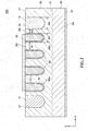
FIG. 3 is a cross-sectional view illustrating the configuration of aSchottky barrier diode 200 according to the second embodiment of the present invention. - As illustrated in
FIG. 3 , in theSchottky barrier diode 200 according to the second embodiment, a plurality ofcenter trenches 60 are formed in thedrift layer 30. Thecenter trenches 60 are all formed at a position overlapping theanode electrode 40 in a plan view. The inner wall of each of thecenter trenches 60 is covered with an insulatingfilm 61 made of HfO2 or the like. The inside of eachcenter trench 60 is filled with the same material theanode electrode 40. When thecenter trenches 60 are formed as in the present embodiment, theanode electrode 40 may be made of a material having a low working function, such as molybdenum (Mo) or copper (Cu). Further, in the present embodiment, the dopant concentration of thedrift layer 30 is increased up to about 5 × 1016 cm-3. Other configurations are basically the same as those of theSchottky barrier diode 100 according to the first embodiment, so the same reference numerals are given to the same elements, and overlapping description will be omitted. - A part of the
drift layer 30 positioned between theadjacent center trenches 60 constitutes a mesa region M1. The mesa region M1 becomes a depletion layer when a backward voltage is applied between theanode electrode 40 and thecathode electrode 50, so that a channel region of thedrift layer 30 is pinched off. Thus, a leak current upon application of the backward voltage can be significantly reduced. - In the Schottky barrier diode having such a structure, an electric field concentrates on the bottom portion of a
center trench 60a positioned at the end portion, making it likely to cause dielectric breakdown at this portion. However, in theSchottky barrier diode 200 according to the present embodiment, the outerperipheral trench 10 is formed at the outer periphery of thecenter trenches 60, an electric field concentrating on thecenter trench 60a at the end portion is alleviated. - As illustrated in
FIG. 3 , a part of thedrift layer 30 positioned between thecenter trench 60a at the end portion and the outerperipheral trench 10 constitutes a mesa region M2. Although there is no particular restriction on the relationship between a mesa width W1 of the mesa region M1 and a mesa width W2 of the mesa region M2,
W1 ≥ W2 is preferably satisfied, and
W1 > W2 is more preferably satisfied. - This is because that the mesa width W1 of the mesa region M1 needs to be ensured to some extent in order to reduce on-resistance and that the smaller the mesa width W2 of the mesa region M2 is, the higher the electric field dispersion effect becomes. However, the lower limit of the mesa width W2 of the mesa region M2 is restricted by processing accuracy.
- Although there is also no particular restriction on the relationship between a width W3 of the
center trench 60 and a width W4 of the outerperipheral trench 10,
W3 ≤ W4 is preferably satisfied, and
W3 < W4 is more preferably satisfied. - This is because that the width W3 of the
center trench 60 needs to be reduced to some extent in order to reduce on-resistance and that the larger the width W4 of the outerperipheral trench 10 is, the higher the electric field dispersion effect becomes. - As described above, the
Schottky barrier diode 200 according to the present embodiment has an effect that can reduce a leak current upon application of a backward voltage, in addition to the effect obtained by theSchottky barrier diode 100 according to the first embodiment. Further, in the present embodiment, the outerperipheral trench 10 and thecenter trench 60 have the same depth, and thus, they can be formed in the same process. - Further, although the inner wall of the
center trench 60 is covered with the insulatingfilm 61, and the inside thereof is filled with the same material as theanode electrode 40 in the present embodiment, the inside of thecenter trench 60 may be filled with a semiconductor material of an opposite conductivity type (p-type, in the present embodiment) without the use of the insulatingfilm 61. -
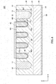
FIG. 4 is a cross-sectional view illustrating the configuration of aSchottky barrier diode 300 according to the third embodiment of the present invention. - As illustrated in
FIG. 4 , in theSchottky barrier diode 300 according to the third embodiment, a depth D2 of the outerperipheral trench 10 is larger than a depth D1 of thecenter trench 60. Other configurations are basically the same as those of theSchottky barrier diode 200 according to the second embodiment, so the same reference numerals are given to the same elements, and overlapping description will be omitted. - When the depth D2 of the outer
peripheral trench 10 is small, the electric field dispersion effect cannot sufficiently be obtained; however, by making the depth D2 of the outerperipheral trench 10 larger than the depth D1 of thecenter trench 60, the electric field dispersion effect can be enhanced. - It is apparent that the present invention is not limited to the above embodiments, but may be modified and changed without departing from the scope and spirit of the invention.
- A simulation model of example 1 having the same configuration as the
Schottky barrier diode 100 illustrated inFIGs. 1 and2 was assumed, and electric field strength was simulated with a backward voltage applied between theanode electrode 40 and thecathode electrode 50. The dopant concentration of thesemiconductor substrate 20 was set to 1 × 1018 cm-3, and the dopant concentration of thedrift layer 30 was to 1 × 1016 cm-3. The thickness of thedrift layer 30 was set to 7 µm. For comparison, a simulation model of comparative example 1 having a structure obtained by removing the outerperipheral trench 10 andinsulator 11 from the simulation model of example 1 was assumed, and electric field strength was simulated with a backward voltage applied between theanode electrode 40 and thecathode electrode 50. -
FIG. 5 is a view illustrating the simulation result of comparative example 1. In the simulation model of comparative example 1, an electric field concentrated on the corner of theanode electrode 40, and the maximum value thereof was 8.3 MV/cm. -
FIG. 6 is a view illustrating the simulation result of example 1. Also in the simulation model of example 1, an electric field concentrated on the corner of theanode electrode 40; however, the electric field was dispersed by the outerperipheral trench 10, with the result that the maximum value thereof was reduced to 6.8 MV/cm. - A simulation model of example 2 having the same configuration as the
Schottky barrier diode 200 illustrated inFIG. 3 was assumed, and electric field strength was simulated with a backward voltage applied between theanode electrode 40 and thecathode electrode 50. The depth D1 and the width W3 of thecenter trench 60 were set to 3 µm and 1 µm, respectively, the mesa width W1 of the mesa region M1 was set to 2 µm, and the insulatingfilm 61 formed on the inner wall of thecenter trench 60 was an HfO2 film having a thickness of 50 nm. On the other hand, the depth D2 and the width W4 of the outerperipheral trench 10 were set to 3 µm and 5 µm, respectively, and the mesa width W2 of the mesa region M2 was set to 2 µm. The dopant concentration of thedrift layer 30 was set to 5 × 1016 cm-3. Other conditions are the same as those of the simulation model of example 1. - For comparison, a simulation model of comparative example 2 having a structure obtained by removing the outer
peripheral trench 10 andinsulator 11 from the simulation model of example 2 was assumed, and electric field strength was simulated with a backward voltage applied between theanode electrode 40 and thecathode electrode 50. -
FIG. 7 is a view illustrating the simulation result of comparative example 2. In the simulation model of comparative example 2, an electric field concentrated on the bottom portion of thecenter trench 60a positioned at the end portion, and the maximum value thereof was 12.1 MV/cm. -
FIG. 8 is a view illustrating the simulation result of example 2. Also in the simulation model of example 2, an electric field concentrated on the bottom portion of thecenter trench 60a positioned at the end portion; however, the electric field was dispersed by the outerperipheral trench 10, with the result that the maximum value thereof was reduced to 11.6 MV/cm. - On the other hand, the electric field concentrated to some extent also at the bottom portion of the
center trench 60 located at a position other than the end portion; however, no difference was observed between example 2 and comparative example 2, and the maximum values thereof were both 9.4 MV/cm. - A simulation model of example 3 having the same configuration as the
Schottky barrier diode 300 illustrated inFIG. 4 was assumed, and electric field strength was simulated with a forward voltage applied between the anode electrode and the cathode electrode. In the simulation model of example 3, the depth D2 of the outerperipheral trench 10 was set to 5 µm. Other conditions are the same as those of the simulation model of example 2. -
FIG. 9 is a graph illustrating the relationship between the depth of the outer peripheral trench and the electric field strength. InFIG. 9 , E1 denotes the maximum electric field applied to thesemiconductor substrate 20 near thecenter trench 60 located at a position other than the end portion, E2 denotes the maximum electric field applied to thesemiconductor substrate 20 near thecenter trench 60a located at the end portion, E3 denotes the maximum electric field applied to the insulatingfilm 61 covering the inner wall of thecenter trench 60 located at a position other than the end portion, and E4 denotes the maximum electric field applied to the insulatingfilm 61 covering the inner wall of thecenter trench 60a located at the end portion. - As illustrated in
FIG. 9 , the electric field applied to thesemiconductor substrate 20 and insulatingfilm 61 near thecenter trench 60a positioned at the end portion was more alleviated as the depth of the outerperipheral trench 10 was increased. On the other hand, the electric field applied to thesemiconductor substrate 20 and insulatingfilm 61 near thecenter trench 60 positioned at a position other than the end portion was constant regardless of the depth of the outerperipheral trench 10. -
- 10
- peripheral trench
- 11
- insulator
- 20
- semiconductor substrate
- 21
- upper surface of semiconductor substrate
- 22
- back surface of semiconductor substrate
- 30
- drift layer
- 31
- upper surface of the drift layer
- 40
- anode electrode
- 50
- cathode electrode
- 60
- center trench
- 60a
- center trench at end portion
- 61
- insulating film
- 100, 200, 300
- Schottky barrier diode
- M1, M2
- mesa region
Claims (7)
- A Schottky barrier diode comprising:a semiconductor substrate made of gallium oxide;a drift layer made of gallium oxide and provided on the semiconductor substrate;an anode electrode brought into Schottky contact with the drift layer; anda cathode electrode brought into ohmic contact with the semiconductor substrate,wherein the drift layer has an outer peripheral trench formed at a position surrounding the anode electrode in a plan view.
- The Schottky barrier diode as claimed in claim 1, further comprising an insulator embedded in the outer peripheral trench.
- The Schottky barrier diode as claimed in claim 1 or 2, wherein the drift layer further has a plurality of center trenches formed at a position overlapping the anode electrode in a plan view.
- The Schottky barrier diode as claimed in claim 3, wherein an inner wall of each of the plurality of center trenches is covered with an insulating film.
- The Schottky barrier diode as claimed in claim 3 or 4, wherein a width of the outer peripheral trench is larger than a width of the center trenches.
- The Schottky barrier diode as claimed in any one of claims 3 to 5, wherein a depth of the outer peripheral trench is larger than a depth of the center trenches.
- The Schottky barrier diode as claimed in any one of claims 3 to 6, wherein a mesa width between the outer peripheral trench and the center trench positioned closest to the outer peripheral trench is smaller than a mesa width between the plurality of center trenches.
Applications Claiming Priority (2)
| Application Number | Priority Date | Filing Date | Title |
|---|---|---|---|
| JP2017173804A JP7147141B2 (en) | 2017-09-11 | 2017-09-11 | schottky barrier diode |
| PCT/JP2018/032086 WO2019049764A1 (en) | 2017-09-11 | 2018-08-30 | Schottky barrier diode |
Publications (2)
| Publication Number | Publication Date |
|---|---|
| EP3683847A1 true EP3683847A1 (en) | 2020-07-22 |
| EP3683847A4 EP3683847A4 (en) | 2021-06-09 |
Family
ID=65634111
Family Applications (1)
| Application Number | Title | Priority Date | Filing Date |
|---|---|---|---|
| EP18854107.2A Pending EP3683847A4 (en) | 2017-09-11 | 2018-08-30 | SCHOTTKY BARRIER DIODE |
Country Status (5)
| Country | Link |
|---|---|
| US (1) | US11699766B2 (en) |
| EP (1) | EP3683847A4 (en) |
| JP (1) | JP7147141B2 (en) |
| CN (1) | CN111095570B (en) |
| WO (1) | WO2019049764A1 (en) |
Families Citing this family (5)
| Publication number | Priority date | Publication date | Assignee | Title |
|---|---|---|---|---|
| US11424239B2 (en) | 2019-12-21 | 2022-08-23 | Intel Corporation | Diodes for package substrate electrostatic discharge (ESD) protection |
| US11264373B2 (en) * | 2019-12-21 | 2022-03-01 | Intel Corporation | Die backend diodes for electrostatic discharge (ESD) protection |
| TW202306179A (en) | 2021-06-07 | 2023-02-01 | 日商Flosfia股份有限公司 | Semiconductor device |
| TW202315140A (en) | 2021-06-07 | 2023-04-01 | 日商Flosfia股份有限公司 | Semiconductor device |
| TWI901178B (en) * | 2023-09-21 | 2025-10-11 | 日商Tdk股份有限公司 | Semiconductor device |
Family Cites Families (31)
| Publication number | Priority date | Publication date | Assignee | Title |
|---|---|---|---|---|
| JP4984345B2 (en) * | 2000-06-21 | 2012-07-25 | 富士電機株式会社 | Semiconductor device |
| JP3914785B2 (en) * | 2002-02-20 | 2007-05-16 | 新電元工業株式会社 | Diode element |
| JP2005243717A (en) | 2004-02-24 | 2005-09-08 | Sanyo Electric Co Ltd | Semiconductor device |
| US9252251B2 (en) * | 2006-08-03 | 2016-02-02 | Infineon Technologies Austria Ag | Semiconductor component with a space saving edge structure |
| JP5101985B2 (en) * | 2007-10-23 | 2012-12-19 | 株式会社日立製作所 | Junction barrier Schottky diode |
| US8344422B2 (en) * | 2007-12-26 | 2013-01-01 | Nec Corporation | Semiconductor device |
| JP5566020B2 (en) * | 2008-12-22 | 2014-08-06 | 新電元工業株式会社 | Manufacturing method of trench Schottky barrier diode |
| US8148749B2 (en) * | 2009-02-19 | 2012-04-03 | Fairchild Semiconductor Corporation | Trench-shielded semiconductor device |
| US7989887B2 (en) * | 2009-11-20 | 2011-08-02 | Force Mos Technology Co., Ltd. | Trench MOSFET with trenched floating gates as termination |
| JP5531620B2 (en) * | 2010-01-05 | 2014-06-25 | 富士電機株式会社 | Semiconductor device |
| JP2012023199A (en) * | 2010-07-14 | 2012-02-02 | Rohm Co Ltd | Schottky barrier diode |
| WO2013035472A1 (en) * | 2011-09-08 | 2013-03-14 | 株式会社タムラ製作所 | Substrate for epitaxial growth, and crystal laminate structure |
| US8809942B2 (en) | 2011-09-21 | 2014-08-19 | Kabushiki Kaisha Toshiba | Semiconductor device having trench structure |
| US20130087852A1 (en) * | 2011-10-06 | 2013-04-11 | Suku Kim | Edge termination structure for power semiconductor devices |
| JP2013102081A (en) | 2011-11-09 | 2013-05-23 | Tamura Seisakusho Co Ltd | Schottky barrier diode |
| JP5999678B2 (en) * | 2011-12-28 | 2016-09-28 | ローム株式会社 | Semiconductor device and manufacturing method of semiconductor device |
| US8884360B2 (en) * | 2012-02-24 | 2014-11-11 | Infineon Technologies Austria Ag | Semiconductor device with improved robustness |
| CN103579371A (en) | 2012-07-27 | 2014-02-12 | 朱江 | Channel terminal structure Schottky device and manufacturing method thereof |
| JP2014078561A (en) * | 2012-10-09 | 2014-05-01 | Rohm Co Ltd | Nitride semiconductor schottky barrier diode |
| JP6202514B2 (en) * | 2012-10-31 | 2017-09-27 | ローム株式会社 | Nitride semiconductor Schottky barrier diode |
| TWI469341B (en) * | 2012-12-20 | 2015-01-11 | Ind Tech Res Inst | Tantalum carbide trench type Schottky barrier element |
| JP2014127573A (en) * | 2012-12-26 | 2014-07-07 | Rohm Co Ltd | Semiconductor device |
| TW201442253A (en) * | 2013-04-19 | 2014-11-01 | Economic Semiconductor Corp | Semiconductor device and its terminal area structure |
| WO2015060441A1 (en) * | 2013-10-24 | 2015-04-30 | ローム株式会社 | Semiconductor device and semiconductor package |
| JP6296445B2 (en) * | 2014-02-10 | 2018-03-20 | ローム株式会社 | Schottky barrier diode |
| CN106415845B (en) | 2014-07-22 | 2019-12-10 | 株式会社Flosfia | Crystalline semiconductor film, plate-like body, and semiconductor device |
| JP2016081946A (en) * | 2014-10-09 | 2016-05-16 | 株式会社Flosfia | Semiconductor structure and semiconductor device |
| JP6647621B2 (en) * | 2015-02-25 | 2020-02-14 | 国立大学法人九州大学 | Impurity introduction device, impurity introduction method, and semiconductor element manufacturing method |
| JP2017045969A (en) | 2015-08-28 | 2017-03-02 | 株式会社タムラ製作所 | Schottky barrier diode |
| JP6662059B2 (en) * | 2016-01-26 | 2020-03-11 | 豊田合成株式会社 | Semiconductor device and power converter |
| CN107026209A (en) * | 2017-04-20 | 2017-08-08 | 中国科学院微电子研究所 | Junction barrier schottky diode based on gallium oxide and preparation method thereof |
-
2017
- 2017-09-11 JP JP2017173804A patent/JP7147141B2/en active Active
-
2018
- 2018-08-30 US US16/646,074 patent/US11699766B2/en active Active
- 2018-08-30 CN CN201880058896.5A patent/CN111095570B/en active Active
- 2018-08-30 WO PCT/JP2018/032086 patent/WO2019049764A1/en not_active Ceased
- 2018-08-30 EP EP18854107.2A patent/EP3683847A4/en active Pending
Also Published As
| Publication number | Publication date |
|---|---|
| WO2019049764A1 (en) | 2019-03-14 |
| US20200287060A1 (en) | 2020-09-10 |
| EP3683847A4 (en) | 2021-06-09 |
| JP7147141B2 (en) | 2022-10-05 |
| CN111095570B (en) | 2023-07-25 |
| CN111095570A (en) | 2020-05-01 |
| JP2019050290A (en) | 2019-03-28 |
| US11699766B2 (en) | 2023-07-11 |
Similar Documents
| Publication | Publication Date | Title |
|---|---|---|
| EP3703137A1 (en) | Schottky barrier diode | |
| US11469334B2 (en) | Schottky barrier diode | |
| US11621357B2 (en) | Schottky barrier diode | |
| US11557681B2 (en) | Schottky barrier diode | |
| US11081598B2 (en) | Trench MOS Schottky diode | |
| US11908955B2 (en) | Schottky barrier diode | |
| US11699766B2 (en) | Schottky barrier diode | |
| US20240313130A1 (en) | Junction barrier schottky diode | |
| US9029210B2 (en) | GaN vertical superjunction device structures and fabrication methods | |
| US20240313129A1 (en) | Schottky barrier diode | |
| US12520510B2 (en) | Schottky barrier diode | |
| EP4300585A1 (en) | Schottky barrier diode | |
| CN120826994A (en) | Junction Barrier Schottky Diode | |
| US20260013157A1 (en) | Schottky barrier diode |
Legal Events
| Date | Code | Title | Description |
|---|---|---|---|
| STAA | Information on the status of an ep patent application or granted ep patent |
Free format text: STATUS: THE INTERNATIONAL PUBLICATION HAS BEEN MADE |
|
| PUAI | Public reference made under article 153(3) epc to a published international application that has entered the european phase |
Free format text: ORIGINAL CODE: 0009012 |
|
| STAA | Information on the status of an ep patent application or granted ep patent |
Free format text: STATUS: REQUEST FOR EXAMINATION WAS MADE |
|
| 17P | Request for examination filed |
Effective date: 20200408 |
|
| AK | Designated contracting states |
Kind code of ref document: A1 Designated state(s): AL AT BE BG CH CY CZ DE DK EE ES FI FR GB GR HR HU IE IS IT LI LT LU LV MC MK MT NL NO PL PT RO RS SE SI SK SM TR |
|
| AX | Request for extension of the european patent |
Extension state: BA ME |
|
| DAV | Request for validation of the european patent (deleted) | ||
| DAX | Request for extension of the european patent (deleted) | ||
| A4 | Supplementary search report drawn up and despatched |
Effective date: 20210511 |
|
| RIC1 | Information provided on ipc code assigned before grant |
Ipc: H01L 29/872 20060101AFI20210505BHEP Ipc: H01L 21/28 20060101ALI20210505BHEP Ipc: H01L 29/06 20060101ALI20210505BHEP Ipc: H01L 29/47 20060101ALI20210505BHEP Ipc: H01L 29/24 20060101ALI20210505BHEP |
|
| STAA | Information on the status of an ep patent application or granted ep patent |
Free format text: STATUS: EXAMINATION IS IN PROGRESS |
|
| 17Q | First examination report despatched |
Effective date: 20220905 |