EP3683682B1 - Busüberwachungssystem, -verfahren und -vorrichtung - Google Patents
Busüberwachungssystem, -verfahren und -vorrichtung Download PDFInfo
- Publication number
- EP3683682B1 EP3683682B1 EP18856083.3A EP18856083A EP3683682B1 EP 3683682 B1 EP3683682 B1 EP 3683682B1 EP 18856083 A EP18856083 A EP 18856083A EP 3683682 B1 EP3683682 B1 EP 3683682B1
- Authority
- EP
- European Patent Office
- Prior art keywords
- bus
- monitoring
- information
- module
- node
- Prior art date
- Legal status (The legal status is an assumption and is not a legal conclusion. Google has not performed a legal analysis and makes no representation as to the accuracy of the status listed.)
- Active
Links
Images



Classifications
-
- G—PHYSICS
- G06—COMPUTING OR CALCULATING; COUNTING
- G06F—ELECTRIC DIGITAL DATA PROCESSING
- G06F11/00—Error detection; Error correction; Monitoring
- G06F11/30—Monitoring
- G06F11/3003—Monitoring arrangements specially adapted to the computing system or computing system component being monitored
- G06F11/3027—Monitoring arrangements specially adapted to the computing system or computing system component being monitored where the computing system component is a bus
-
- G—PHYSICS
- G06—COMPUTING OR CALCULATING; COUNTING
- G06F—ELECTRIC DIGITAL DATA PROCESSING
- G06F11/00—Error detection; Error correction; Monitoring
- G06F11/07—Responding to the occurrence of a fault, e.g. fault tolerance
- G06F11/0703—Error or fault processing not based on redundancy, i.e. by taking additional measures to deal with the error or fault not making use of redundancy in operation, in hardware, or in data representation
- G06F11/0751—Error or fault detection not based on redundancy
-
- G—PHYSICS
- G06—COMPUTING OR CALCULATING; COUNTING
- G06F—ELECTRIC DIGITAL DATA PROCESSING
- G06F11/00—Error detection; Error correction; Monitoring
- G06F11/07—Responding to the occurrence of a fault, e.g. fault tolerance
-
- G—PHYSICS
- G06—COMPUTING OR CALCULATING; COUNTING
- G06F—ELECTRIC DIGITAL DATA PROCESSING
- G06F11/00—Error detection; Error correction; Monitoring
- G06F11/07—Responding to the occurrence of a fault, e.g. fault tolerance
- G06F11/0703—Error or fault processing not based on redundancy, i.e. by taking additional measures to deal with the error or fault not making use of redundancy in operation, in hardware, or in data representation
- G06F11/0766—Error or fault reporting or storing
- G06F11/0772—Means for error signaling, e.g. using interrupts, exception flags, dedicated error registers
-
- G—PHYSICS
- G06—COMPUTING OR CALCULATING; COUNTING
- G06F—ELECTRIC DIGITAL DATA PROCESSING
- G06F11/00—Error detection; Error correction; Monitoring
- G06F11/07—Responding to the occurrence of a fault, e.g. fault tolerance
- G06F11/0703—Error or fault processing not based on redundancy, i.e. by taking additional measures to deal with the error or fault not making use of redundancy in operation, in hardware, or in data representation
- G06F11/0766—Error or fault reporting or storing
- G06F11/0787—Storage of error reports, e.g. persistent data storage, storage using memory protection
-
- G—PHYSICS
- G06—COMPUTING OR CALCULATING; COUNTING
- G06F—ELECTRIC DIGITAL DATA PROCESSING
- G06F11/00—Error detection; Error correction; Monitoring
- G06F11/07—Responding to the occurrence of a fault, e.g. fault tolerance
- G06F11/0703—Error or fault processing not based on redundancy, i.e. by taking additional measures to deal with the error or fault not making use of redundancy in operation, in hardware, or in data representation
- G06F11/0793—Remedial or corrective actions
-
- G—PHYSICS
- G06—COMPUTING OR CALCULATING; COUNTING
- G06F—ELECTRIC DIGITAL DATA PROCESSING
- G06F11/00—Error detection; Error correction; Monitoring
- G06F11/07—Responding to the occurrence of a fault, e.g. fault tolerance
- G06F11/08—Error detection or correction by redundancy in data representation, e.g. by using checking codes
- G06F11/10—Adding special bits or symbols to the coded information, e.g. parity check, casting out 9's or 11's
- G06F11/1008—Adding special bits or symbols to the coded information, e.g. parity check, casting out 9's or 11's in individual solid state devices
- G06F11/1012—Adding special bits or symbols to the coded information, e.g. parity check, casting out 9's or 11's in individual solid state devices using codes or arrangements adapted for a specific type of error
- G06F11/1016—Error in accessing a memory location, i.e. addressing error
-
- G—PHYSICS
- G06—COMPUTING OR CALCULATING; COUNTING
- G06F—ELECTRIC DIGITAL DATA PROCESSING
- G06F11/00—Error detection; Error correction; Monitoring
- G06F11/07—Responding to the occurrence of a fault, e.g. fault tolerance
- G06F11/14—Error detection or correction of the data by redundancy in operations
- G06F11/1402—Saving, restoring, recovering or retrying
- G06F11/1405—Saving, restoring, recovering or retrying at machine instruction level
- G06F11/141—Saving, restoring, recovering or retrying at machine instruction level for bus or memory accesses
-
- G—PHYSICS
- G06—COMPUTING OR CALCULATING; COUNTING
- G06F—ELECTRIC DIGITAL DATA PROCESSING
- G06F11/00—Error detection; Error correction; Monitoring
- G06F11/22—Detection or location of defective computer hardware by testing during standby operation or during idle time, e.g. start-up testing
- G06F11/2205—Detection or location of defective computer hardware by testing during standby operation or during idle time, e.g. start-up testing using arrangements specific to the hardware being tested
- G06F11/221—Detection or location of defective computer hardware by testing during standby operation or during idle time, e.g. start-up testing using arrangements specific to the hardware being tested to test buses, lines or interfaces, e.g. stuck-at or open line faults
-
- G—PHYSICS
- G06—COMPUTING OR CALCULATING; COUNTING
- G06F—ELECTRIC DIGITAL DATA PROCESSING
- G06F11/00—Error detection; Error correction; Monitoring
- G06F11/30—Monitoring
- G06F11/3051—Monitoring arrangements for monitoring the configuration of the computing system or of the computing system component, e.g. monitoring the presence of processing resources, peripherals, I/O links, software programs
-
- G—PHYSICS
- G06—COMPUTING OR CALCULATING; COUNTING
- G06F—ELECTRIC DIGITAL DATA PROCESSING
- G06F11/00—Error detection; Error correction; Monitoring
- G06F11/30—Monitoring
- G06F11/34—Recording or statistical evaluation of computer activity, e.g. of down time, of input/output operation ; Recording or statistical evaluation of user activity, e.g. usability assessment
- G06F11/3466—Performance evaluation by tracing or monitoring
- G06F11/349—Performance evaluation by tracing or monitoring for interfaces, buses
-
- G—PHYSICS
- G06—COMPUTING OR CALCULATING; COUNTING
- G06F—ELECTRIC DIGITAL DATA PROCESSING
- G06F11/00—Error detection; Error correction; Monitoring
- G06F11/36—Prevention of errors by analysis, debugging or testing of software
- G06F11/362—Debugging of software
- G06F11/3636—Debugging of software by tracing the execution of the program
- G06F11/364—Debugging of software by tracing the execution of the program tracing values on a bus
-
- G—PHYSICS
- G06—COMPUTING OR CALCULATING; COUNTING
- G06F—ELECTRIC DIGITAL DATA PROCESSING
- G06F21/00—Security arrangements for protecting computers, components thereof, programs or data against unauthorised activity
- G06F21/70—Protecting specific internal or peripheral components, in which the protection of a component leads to protection of the entire computer
- G06F21/82—Protecting input, output or interconnection devices
- G06F21/85—Protecting input, output or interconnection devices interconnection devices, e.g. bus-connected or in-line devices
-
- G—PHYSICS
- G06—COMPUTING OR CALCULATING; COUNTING
- G06F—ELECTRIC DIGITAL DATA PROCESSING
- G06F11/00—Error detection; Error correction; Monitoring
- G06F11/30—Monitoring
- G06F11/3065—Monitoring arrangements determined by the means or processing involved in reporting the monitored data
-
- G—PHYSICS
- G06—COMPUTING OR CALCULATING; COUNTING
- G06F—ELECTRIC DIGITAL DATA PROCESSING
- G06F2201/00—Indexing scheme relating to error detection, to error correction, and to monitoring
- G06F2201/86—Event-based monitoring
Definitions
- the present disclosure relates to the field of processors, and in particular to a bus monitoring system, method and apparatus.
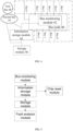
- FIG.1 is a diagram of a bus monitoring apparatus in the related art of the present disclosure. In this way, if bus exception occurs, the processors or the peripherals cannot be accessed through the bus, thus it is impossible to acquire bus monitoring information, which further makes it difficult to locate the fault.
- Document EP 2 472 408 A1 discloses a bus monitor for increasing system safety of System On Chip (SOC) and a realizing method thereof.
- SOC System On Chip
- the embodiments of the present disclosure provide a bus monitoring system, a method and an apparatus, to solve at least the technical problem that bus monitoring information cannot be acquired in case of bus exceptions in the related art.
- a second bus is added on the basis of a first bus, and the second bus is used for acquiring monitoring information to ensure that the bus monitoring information can also be acquired in case of bus exceptions, which solves the technical problem that bus monitoring information cannot be acquired in case of bus exceptions in the related art, and improves the bus node monitoring efficiency.
- FIG. 2 is a flowchart of a bus monitoring method according to an embodiment of the present disclosure. As shown in FIG. 2 , the flowchart includes the following steps.
- a second bus is added on the basis of the first bus, and the second bus is used for acquiring monitoring information, so that the bus monitoring information can also be acquired in case of bus exceptions, which solves the technical problem that the bus monitoring information cannot be acquired in case of bus exceptions in the related art, and improves the bus node monitoring efficiency.
- the execution body of the above steps may be a bus node, specifically be but not limited to a processor, a chip, a bus management device, and the like.
- Step S204 the scheme of the embodiment further includes: Step S206, saving the monitoring information.
- the step of acquiring the monitoring information from the bus monitoring module through the second bus includes one steps of:
- the step of saving the monitoring information may be but not limited to, saving the monitoring information into a local ROM space; saving the monitoring information into a local RAM space; saving the monitoring information into a remote ROM space; and saving the monitoring information into a remote RAM space.
- the ROM may be Flash
- the RAM may be DDR (Double Data Rate SDRAM).
- the method further includes:
- the step of executing the reset operation on the chip where the bus node is located includes executing the reset operation on the chip where the bus node is located, when detecting an indication that the monitoring information is saved.
- the step of performing fault analysis based on the monitoring information includes:
- the step of performing fault analysis based on the monitoring information includes:
- the method further includes:
- the step of acquiring the monitoring information from the bus monitoring module through the second bus includes: when the current access information indicates that the bus node is abnormal, acquiring the monitoring information from the bus monitoring module through the second bus; and when the current access information indicates that the bus node is normal, acquiring the monitoring information from the bus monitoring module through the second bus.
- the step of monitoring the first bus where the bus monitoring module is located to generate monitoring information includes: monitoring the access information of the bus node through the first bus, and storing the access information to the bus monitoring module to obtain the monitoring information of the bus node.
- the technical solutions of the present disclosure may be embodied in the form of a software product, which is stored in a storage medium (e.g., ROM/RAM, magnetic disk, optical disk) and includes instructions for enabling a terminal device (e.g., a mobile phone, a computer, a server, or a network device) to execute the method according to the embodiments of the present disclosure.
- a storage medium e.g., ROM/RAM, magnetic disk, optical disk
- a terminal device e.g., a mobile phone, a computer, a server, or a network device
- a bus monitoring apparatus and a bus monitoring system are further provided for implementing the foregoing embodiments and preferred implementations.
- the description which has been set fourth will be omitted.
- the term "module" can implement a combination of software and/or hardware with predetermined functions.
- the apparatus described by the following embodiments is preferably implemented by software, it is also possible and conceivable to implement the apparatus by hardware or a combination of software and hardware.
- FIG. 3 is a block diagram illustrating a structure of a bus monitoring apparatus according to an embodiment of the present disclosure.
- the bus monitoring apparatus is applicable to a chip or the like, particularly a multiprocessor chip. As shown in FIG. 3 , the bus monitoring apparatus includes:
- the apparatus further includes a storage module configured to store the monitoring information.
- the acquisition module includes one of: a first acquisition unit configured to acquire the monitoring information from the bus monitoring module through the second bus according to event trigger; a second acquisition unit configured to acquire the monitoring information from the bus monitoring module through the second bus according to query state; and a third acquisition unit configured to acquire the monitoring information from the bus monitoring module through the second bus according to continuous storage.
- the apparatus further includes: a reset module configured to execute a reset operation on the chip where the bus node is located after the storage module saves the monitoring information; a fault analysis module configured to perform fault analysis based on the monitoring information.
- the apparatus further includes: a determination module configured to determine a fault bus node after the analysis module performs the fault analysis based on the monitoring information; a detection module configured to detect whether the access address of the fault bus node is legal or not when the current bus node initiates access; a processing module configured to prohibit access to the fault bus node when the access address of the fault bus node is illegal.
- FIG. 4 is a block diagram illustrating a structure of a bus monitoring system according to an embodiment of the present disclosure. As shown in FIG. 4 , the bus monitoring system includes:
- system further includes a storage module 46 configured to store the monitoring information.
- second bus is also configured to connect the information storage module and the storage module.
- the second bus is further configured to perform at least one of: backing up data of a chip where the bus node is located, and expanding traffic flow of a path for a designated use.
- the system further includes: a chip reset module configured to perform a reset operation on a chip where the bus node is located, when detecting an indication that the monitoring information is saved; and a fault analysis module configured to perform fault analysis based on the monitoring information.
- a chip reset module configured to perform a reset operation on a chip where the bus node is located, when detecting an indication that the monitoring information is saved
- a fault analysis module configured to perform fault analysis based on the monitoring information.
- the above modules may be implemented by software or hardware.
- the hardware may be implemented by, but not limited to, the above-described modules located in the same processor; or the above-described modules located in different processors in any combination.
- the present embodiment is an alternative embodiment according to the present disclosure, and is used for supplementing and detailing the present application in combination with specific examples and scenarios.
- the embodiment provides a method for storing bus node information in a multiprocessor chip by adding a second bus and an information storage module on the basis of a bus monitoring module, so as to ensure that when a bus exception occurs, bus monitoring information can be acquired and exception analysis can be performed.
- the scheme of the embodiment ensures that the monitoring information of the bus node can be acquired in case of bus exceptions, thereby locating fault quickly and accurately.
- the multiprocessor chip bus monitoring apparatus described in the present disclosure includes the following modules: a bus monitoring module, an information storage module, a memory, a chip reset module, and a fault analysis module.
- FIG. 5 is a block diagram of the bus monitoring apparatus according to the embodiment of the present disclosure.
- the information storage module of the device of the present disclosure reads the monitoring information from the bus monitoring module (monitoring the first bus) through the second bus (shown in FIG. 4 ) and stores the information into the memory; and, after the storage is completed, informs the chip reset module to reset the chip; and the fault analysis module acquires the monitoring information from the memory to perform exception analysis.
- the first bus (buses 0-N shown in FIG. 4 all belong to the first bus) is a path connecting a master device and a slave device.
- Master devices such as processors and peripherals access slave devices such as DDR and bus monitoring unit through the first bus.
- the second bus is used for the information storage module to access the bus monitoring module and the memory, and the monitoring information of the bus monitoring module is stored in the memory through the second bus.
- the second bus is independent of the first bus, namely, when exception occurs at the first bus, the second bus can also access the bus monitoring module;
- the second bus can also be used for backing up the chip, and expanding the traffic flow.
- the bus nodes are a plurality of bus (bus 0-bus N) inlets and outlets, and the bus monitoring module can monitor one or more bus nodes.
- the bus monitoring module is responsible for capturing bus (bus 0-bus N) access information of the bus nodes; the bus monitoring module includes a configuration part, a monitoring part and an event generating part.
- the configuration part receives configuration information, the monitoring part monitors the bus according to the configuration and writes the captured monitoring information into a register space of the bus monitoring module; an event generating part generates an event in case of exception and sets an exception state.
- the information storage module is responsible for bus monitoring information storage and memory space management; the information storage module includes a configuration part, a read-write operation part and an event processing part.
- FIG. 6 is a diagram illustrating a structure of an information storage module according to the embodiment of the present disclosure (see FIG. 6 , diagram illustrating a structure of the information storage module).
- the information storage module uses a second bus, the second bus being independent of the first bus where the bus monitoring module is located, so that the information storage module can also execute operation in case of bus exceptions.
- the configuration part mainly configures operation modes, including query, event trigger and continuous storage.
- the query mode refers to inquiring the state of the bus monitoring module;
- the event trigger refers to responding to the exception event of the bus monitoring module;
- the continuous storage mode refers to that the information storage module continuously stores access information captured by the bus monitoring module.
- the read-write operation part writes the monitoring information of the bus monitoring module into the memory, and the operation mode being controlled by configuration.
- the read-write operation part manages the storage space of the memory according to the bus nodes, to ensure the exactness of the information of each bus node.
- the event processing part mainly receives exception events sent by the bus monitoring module, generates read-write completion events and sets completion flags after the storage operation is completed.
- the information storage module may complete information storage of one or more bus monitoring modules.
- the memory may be a ROM/RAM space in the monitoring bus chip or an RAM/ROM space outside the chip for storing monitoring information.
- the chip reset module executes a chip reset operation.
- the chip reset module is mainly responsible for inquiring the execution state of the information storage module or receiving completion events transmitted from the information storage module, and executing the chip reset operation according to the state or event.
- the fault analysis module is responsible for problem locating analysis, and in case of bus exceptions, deducing the chip access model according to the access information of the bus monitoring node in the memory, and finding out abnormal access.
- the operation modes include event trigger, query state, and continuous storage.
- the memory may be an on/off-chip ROM , such as Flash, or an on/off-chip RAM, such as DDR; in the case of RAM, it is necessary to ensure that information is not lost during the reset process.
- an on/off-chip ROM such as Flash
- an on/off-chip RAM such as DDR
- the information storage module After the completion of the storage, the information storage module generates a completion event and sets a completion flag indicating that the storage is completed.
- the chip reset module resets the chip.
- Step 3 the fault analysis module exports bus monitoring information from the memory, analyzes the exception reason and obtains an analysis result, and performs targeted protection and repair based on the analysis result.
- FIG.7 is a diagram of a bus topology configuration illustrating a structure of an embodiment of the present disclosure.
- Each master (master device) is connected to a bus node, wherein the bus nodes are interconnected, and finally connected to slave devices.
- bus node 4 is connected to master 7, the nodes at the upper level of connection are bus node 0 and bus node 1, and the nodes at the lower level of connection are bus node 5 and bus node 6.
- a chip bus subsystem numbers the masters and the monitoring nodes uniformly, monitors the bus nodes when the system runs, stores the bus node information, exports the monitoring bus node information in case of bus exceptions, analyzes the node information, connects the access numbers, and establishes an access model.
- the present embodiment also includes the following examples.
- the present implementation provides an embodiment for locating a bus exception by acquiring information using event mode.
- FIG. 8 is a flowchart of locating a bus exception by using event mode according to an embodiment of the present disclosure, where the processing steps of the flow are as follows.
- Step 1 initializing the bus monitoring module, configuring monitoring information for each bus node.
- Serial numbers for masters and bus nodes are configured such to uniformly number the masters and nodes, respectively.
- Address range for monitoring is configured to be address space of the whole chip.
- Step 2 initializing the information storage module.
- Operation mode is configured to be event trigger
- Step 3 capturing access information. After Steps 1) and 2), the bus monitoring module starts to capture information, and each bus node saves the information into a capture register.
- Step 4 saving the monitoring information.
- the bus monitoring module In case of bus exceptions, the bus monitoring module generates an event and sends the event to the information storage module.
- the information storage module After receiving the event, the information storage module reads the monitoring information from the capture register of each bus node.
- the monitoring information of each bus node is saved in a designated space, the information storage module sets a completion flag and generates a completion event after completing the storage.
- Step 5 resetting chip.
- the chip reset module executes chip reset after inquiring the setting of the completion flag or receiving the completion event.
- the processor After the chip is reset, the processor reads the monitoring information from the ROM and saves the information into a file.
- Step 6 exporting and analyzing the monitoring information and locating the bus exception reason by a fault analysis module.
- All the masters are traversed to read the serial numbers of bus nodes directly connected with the current master.
- Access information of a corresponding bus node is read according to the serial number of the bus node; The access information is analyzed to detect whether the current master initiates access to the bus node or not according to the master serial number.
- Step 7 performing address protection on the master of the illegal access address.
- the master Before the master initiates access, it is detected whether the access address is legal or not, wherein if the access address is illegal, prohibit access to the illegal address.
- the present implementation provides an embodiment for locating bus exception by acquiring information using query mode.
- FIG. 9 is a flowchart of locating a bus exception by using query mode according to an embodiment of the present disclosure, where the processing steps of the flow are as follows.
- the implementation provides an embodiment for locating bus exceptions by using information saved in RAM.
- RAM has a higher speed.
- FIG. 10 is a flowchart illustrating a bus exception locating process by using information saved in RAM according to an embodiment of the present disclosure, and the processing steps of the flow are as follows.
- Step 1 the same as that of Implementation One.
- Step 2 initialize the information storage module.
- Operation mode is configured to be event-trigger.
- Node range is configured to be all bus nodes.
- Step 3 the same as that of Implementation One
- Step 4 save monitoring information
- the bus monitoring module In case of bus exceptions, the bus monitoring module generates an event and sends the event to the information storage module.
- the information storage module After receiving the event, the information storage module reads monitoring information from capture registers of the respective bus nodes.
- the monitoring information of the respective bus nodes is save in the RAM by utilizing the characteristic that the space content of the RAM does not lose, and the information storage module sets a completion flag and generates a completion event after completing the storage.
- the chip reset module executes chip reset after inquiring the setting of the completion flag or receiving the completion event.
- the RAM is an on-chip space, it is necessary to ensure that the chip reset type is power-on reset. If the RAM is an off-chip space, the chip where the memory is located is ensured to be power-on reset.
- Step 6 and Step 7 are the same as that of Implementation One.
- the implementation provides an information storage module which, after started, save the bus monitoring information until a bus exception event is received.
- FIG. 11 is a flowchart illustrating a bus exception locating process using continuous storage mode according to the embodiment of the present disclosure.
- the present embodiment can locate bus exceptions in some more complex scenarios.
- Step 1 initialize the bus monitoring module, and configure monitoring information for each bus node.
- Serial numbers for masters and bus nodes are configured such to uniformly number the masters and nodes, respectively.
- Address range monitored is configured to be an address space of the whole chip.
- Access attribute is configured to be read-write.
- Monitoring mode is configured to be continuous monitoring mode.
- Bus monitoring is enabled.
- Step 2 initialize the information storage module
- Operation mode is configured to be continuous storage, and the number of continuous storage is configurable.
- Node range is all bus nodes.
- Step 3 the same as that of Implementation One.
- Step 4 monitor information storage
- the information storage module detects that information is written into bus monitoring, the monitoring information is written into a corresponding RAM space.
- the bus monitoring module When bus exception is triggered, the bus monitoring module generates an event number and informs the information storage module.
- the information storage module sets a completion flag and generates a completion event after completing the saving.
- the chip reset module executes on-power chip reset; Step 6, the fault analysis module exports and analyzes the monitoring information to locate the bus exception reason.
- the monitoring information is sequentially read until the last piece of information.
- All masters are traversed to read the serial number of the bus node directly connected with the current master.
- Historical access information of the corresponding bus node is read according to the serial number of the bus node.
- Historical access information is analyzed to detect whether the current master initiates access or not according to the master serial number
- Step 7 perform address protection on the master of an illegal accessaddress.
- an information storage module a second bus and a memory are added on the basis of the bus monitoring module, so that the bus monitoring information can be acquired in case of bus exceptions.
- the fault analysis module locates bus exception reason quickly, performs protection and corrects errors according to the analysis result, thereby preventing bus exception from being triggered again and improving the stability of the system.
- An embodiment of the present disclosure also provides a storage medium.
- the storage medium may be configured to store a program code for performing steps of:
- the storage medium may include, but is not limited to, a U-disk, a Read-Only Memory (ROM), a Random Access Memory (RAM), a removable hard disk, a magnetic or optical disk, and various other media capable of storing program codes.
- the processor performs monitoring on the first bus where the bus monitoring module is located according to a program code stored in the storage medium, to generates monitoring information;
- the processor acquires the monitoring information from the bus monitoring module through the second bus according to the program code stored in the storage medium.
- modules or steps of the present disclosure may be implemented by general-purpose computing devices, which may be integrated onto a single computing device, or distributed over a network composed of a plurality of computing devices.
- the modules or steps may be implemented by program codes which are executable by computing devices, so that they can be stored in a storage device for execution by computing devices.
- the illustrated or described steps may be performed in an order different from that described herein, or may be made into integrated circuit modules, or a plurality modules or steps among the modules or steps described herein may be made into a single integrated circuit module.
- the present disclosure is not limited to any specific combination of hardware and software.
Landscapes
- Engineering & Computer Science (AREA)
- Theoretical Computer Science (AREA)
- Physics & Mathematics (AREA)
- General Engineering & Computer Science (AREA)
- General Physics & Mathematics (AREA)
- Quality & Reliability (AREA)
- Computing Systems (AREA)
- Computer Hardware Design (AREA)
- Mathematical Physics (AREA)
- Computer Security & Cryptography (AREA)
- Software Systems (AREA)
- Debugging And Monitoring (AREA)
- Multi Processors (AREA)
- Bus Control (AREA)
Claims (13)
- Busüberwachungssystem, Folgendes umfassend:einen Busknoten (40),ein Busüberwachungsmodul (42), das dafür konfiguriert ist, einen ersten Bus (48) zu überwachen, wobei das Busüberwachungsmodul (42) dafür angeordnet ist, Überwachungsinformationen zu erzeugen,ein Informationenspeichermodul (44), das dafür konfiguriert ist, die Überwachungsinformationen von dem Busüberwachungsmodul (42) durch einen zweiten Bus (50) zu erfassen,wobei der erste Bus (48) dafür konfiguriert ist, ein übergeordnetes Gerät und ein untergeordnetes Gerät des Busknotens (40) zu verbinden, undder zweite Bus (50) dafür konfiguriert ist, das Informationenspeichermodul (44) und das Busüberwachungsmodul (42) zu verbinden,wobei der zweite Bus (50) von dem ersten Bus (48) unabhängig ist, der erste Bus (48) ein Pfad ist, der das übergeordnete Gerät und das untergeordnete Gerät verbindet und aus mehreren Bussen besteht, der Busknoten (40) ein Buseingang und - ausgang ist und jedes übergeordnete Gerät mit dem Busknoten verbunden ist,wobei das Busüberwachungsmodul (42) ferner dafür konfiguriert ist, Ausnahmen zu identifizieren und die Überwachungsinformationen für das Informationenspeichermodul (44) über den zweiten Bus bereitzustellen, um adäquate Aktionen vorzunehmen,wobei das Informationenspeichermodul (44) ferner für Folgendes konfiguriert ist:wenn aktuelle Zugriffsinformationen angeben, dass der Busknoten anomal ist, Erfassen der Überwachungsinformationen von dem Busüberwachungsmodul durch den zweiten Bus, undwenn die aktuellen Zugriffsinformationen angeben, dass der Busknoten normal ist, Erfassen der Überwachungsinformationen von dem Busüberwachungsmodul durch den zweiten Bus.
- System nach Anspruch 1, wobei der zweite Bus (50) ferner dafür konfiguriert ist, mindestens eines des Folgenden durchzuführen: Datensicherung eines Chips, auf dem sich der Busknoten (40) befindet, und Erweitern eines Verkehrsflusses eines Pfades.
- System nach Anspruch 1, wobei das System ferner Folgendes umfasst:ein Chipzurücksetzungsmodul, das dafür konfiguriert ist, eine Zurücksetzungsoperation an dem Chip auszuführen, auf dem sich der Busknoten (40) befindet, wenn eine Angabe erkannt wird, dass die Überwachungsinformationen gesichert sind, undein Fehleranalysemodul, das dafür konfiguriert ist, basierend auf den Überwachungsinformationen eine Fehleranalyse durchzuführen.
- System nach Anspruch 1, wobei das System ferner Folgendes umfasst: ein Speichermodul, das dafür konfiguriert ist, die Überwachungsinformationen zu sichern, und
der zweite Bus (50) ferner dafür konfiguriert ist, das Informationsspeichermodul und das Speichermodul zu verbinden. - Busüberwachungsverfahren, Folgendes umfassend:Überwachen (S202) eines ersten Busses, wobei ein Busüberwachungsmodul dafür angeordnet ist, Überwachungsinformationen zu erzeugen,Erfassen (S204) der Überwachungsinformationen von dem Busüberwachungsmodul (42) durch einen zweiten Bus (50),wobei der zweite Bus (50) von dem ersten Bus (48) unabhängig ist, wobei der erste Bus (48) dafür konfiguriert ist, ein übergeordnetes Gerät und ein untergeordnetes Gerät des Busknotens (40) zu verbinden, und der zweite Bus (50) dafür konfiguriert ist, das Informationenspeichermodul (44) und das Busüberwachungsmodul (42) zu verbinden,wobei der erste Bus (48) ein Pfad ist, der das übergeordnete Gerät und das untergeordnete Gerät verbindet und aus mehreren Bussen besteht, der Busknoten (40) ein Buseingang und -ausgang ist und jedes übergeordnete Gerät mit diesem Busknoten verbunden ist, wobei der Schritt des Erfassens der Überwachungsinformationen von dem Busüberwachungsmodul durch den zweiten Bus Folgendes umfasst:wenn aktuelle Zugriffsinformationen angeben, dass der Busknoten anomal ist, Erfassen der Überwachungsinformationen von dem Busüberwachungsmodul durch den zweiten Bus undwenn die aktuellen Zugriffsinformationen angeben, dass der Busknoten normal ist, Erfassen der Überwachungsinformationen von dem Busüberwachungsmodul durch den zweiten Bus.wobei das Verfahren ferner das Identifizieren von Ausnahmen und das Bereitstellen der Überwachungsinformationen für das Informationenspeichermodul (44) über den zweiten Bus, um adäquate Aktionen vorzunehmen, umfasst.
- Verfahren nach Anspruch 5, wobei der Schritt des Erfassens der Überwachungsinformationen von dem Busüberwachungsmodul durch den zweiten Bus eines des Folgenden umfasst:Erfassen der Überwachungsinformationen von dem Busüberwachungsmodul (42) durch den zweiten Bus gemäß einem Ereignisauslöser,Erfassen der Überwachungsinformationen von dem Busüberwachungsmodul (42) durch den zweiten Bus gemäß einem Abfragezustand undErfassen der Überwachungsinformationen von dem Busüberwachungsmodul (42) durch den zweiten Bus (50) gemäß permanenter Speicherung.
- Verfahren nach Anspruch 5, wobei das Verfahren nach dem Erfassen der Überwachungsinformationen von dem Busüberwachungsmodul durch den zweiten Bus ferner Folgendes umfasst:
Sichern der Überwachungsinformationen. - Verfahren nach Anspruch 5, wobei das Verfahren nach dem Sichern der Überwachungsinformationen ferner Folgendes umfasst:Ausführen einer Zurücksetzungsoperation an einem Chip, auf dem sich der Busknoten befindet, undnach Abschluss der Zurücksetzungsoperation Durchführen einer Fehleranalyse, basierend auf den Überwachungsinformationen.
- Verfahren nach Anspruch 8, wobei der Schritt des Ausführens einer Zurücksetzungsoperation an einem Chip, auf dem sich der Busknoten befindet, Folgendes umfasst:
Ausführen der Zurücksetzungsoperation an dem Chip, auf dem sich der Busknoten (40) befindet, wenn eine Angabe erkannt wird, dass die Überwachungsinformationen gesichert wurden. - Verfahren nach Anspruch 9, wobei der Schritt des Durchführens der Fehleranalyse, basierend auf den Überwachungsinformationen, Folgendes umfasst:Ableiten eines Zugriffsmodells des Chips, basierend auf den Überwachungsinformationen, undLokalisieren einer Fehlerart gemäß dem Zugriffsmodell.
- Verfahren nach Anspruch 8, wobei der Schritt des Durchführens der Fehleranalyse, basierend auf den Überwachungsinformationen, Folgendes umfasst:Traversieren aller übergeordneten Geräte, um eine Seriennummer eines Busknotens zu lesen, der direkt mit einem aktuellen übergeordneten Gerät verbunden ist,Lesen historischer Zugriffsinformationen eines entsprechenden Busknotens gemäß der Seriennummer des Busknotens,Analysieren der historischen Zugriffsinformationen, um zu erkennen, ob das aktuelle übergeordnete Gerät einen Zugriff auslöst,wenn der Zugriff ausgelöst wird, Bewerten, ob eine Zugriffsadresse in einem legalen Bereich liegt oder nicht,wenn die Zugriffsadresse nicht in einem legalen Bereich liegt, Aufzeichnen mindestens einer der folgenden Knoteninformationen: Seriennummer des übergeordneten Geräts, Zugriffsadresse und Zugriffattribut undLokalisieren des übergeordneten Geräts mit illegalem Zugriff gemäß der Knoteninformation.
- Verfahren nach Anspruch 8, wobei das Verfahren nach dem Durchführen der Fehleranalyse, basierend auf den Überwachungsinformationen, ferner Folgendes umfasst:Bestimmen eines fehlerhaften Busknotens,wenn ein aktueller Busknoten Zugriff auslöst, Erkennen, ob eine Zugriffsadresse des fehlerhaften Busknotens legal ist oder nicht, undwenn die Zugriffsadresse des fehlerhaften Busknotens illegal ist, Unterbinden des Zugriffs auf den fehlerhaften Busknoten.
- Verfahren nach Anspruch 5, wobei der Schritt des Überwachens des ersten Busses, in dem sich das Busüberwachungsmodul befindet, um die Überwachungsinformationen zu erzeugen, Folgendes umfasst:
Überwachen der Zugriffsinformationen des Busknotens durch den ersten Bus und Sichern der Zugriffsinformationen in einem Busüberwachungsmodul, um die Überwachungsinformationen des Busknotens zu gewinnen.
Applications Claiming Priority (2)
| Application Number | Priority Date | Filing Date | Title |
|---|---|---|---|
| CN201710819085.XA CN109491856B (zh) | 2017-09-12 | 2017-09-12 | 总线监控系统、方法及装置 |
| PCT/CN2018/095429 WO2019052275A1 (zh) | 2017-09-12 | 2018-07-12 | 总线监控系统、方法及装置 |
Publications (3)
| Publication Number | Publication Date |
|---|---|
| EP3683682A1 EP3683682A1 (de) | 2020-07-22 |
| EP3683682A4 EP3683682A4 (de) | 2021-06-16 |
| EP3683682B1 true EP3683682B1 (de) | 2023-11-29 |
Family
ID=65688015
Family Applications (1)
| Application Number | Title | Priority Date | Filing Date |
|---|---|---|---|
| EP18856083.3A Active EP3683682B1 (de) | 2017-09-12 | 2018-07-12 | Busüberwachungssystem, -verfahren und -vorrichtung |
Country Status (5)
| Country | Link |
|---|---|
| US (1) | US11093361B2 (de) |
| EP (1) | EP3683682B1 (de) |
| JP (1) | JP2020525944A (de) |
| CN (1) | CN109491856B (de) |
| WO (1) | WO2019052275A1 (de) |
Families Citing this family (4)
| Publication number | Priority date | Publication date | Assignee | Title |
|---|---|---|---|---|
| CN113268367B (zh) * | 2021-04-26 | 2023-07-14 | 北京控制工程研究所 | 一种1553b总线rt端子地址查找表在轨监测及维护方法 |
| CN113778734B (zh) * | 2021-09-02 | 2024-07-12 | 上海砹芯科技有限公司 | 芯片、芯片总线的检测系统、检测方法及存储介质 |
| CN114531371A (zh) * | 2022-02-23 | 2022-05-24 | 杭州中天微系统有限公司 | 总线监测网络、片上系统以及总线管理方法 |
| CN118939484A (zh) * | 2023-05-10 | 2024-11-12 | 北京有竹居网络技术有限公司 | 总线异常检测和处理方法、装置、系统、设备及介质 |
Family Cites Families (24)
| Publication number | Priority date | Publication date | Assignee | Title |
|---|---|---|---|---|
| JPH02284249A (ja) | 1989-04-26 | 1990-11-21 | Toshiba Corp | バストレーサ |
| JPH11203174A (ja) | 1998-01-19 | 1999-07-30 | Nec Corp | 状態監視情報処理装置 |
| US6425009B1 (en) * | 1999-06-08 | 2002-07-23 | Cisco Technology, Inc. | Monitoring redundant control buses to provide a high availability local area network for a telecommunications device |
| JP2003177975A (ja) | 2001-12-12 | 2003-06-27 | Yokogawa Electric Corp | バスデータアナライザ用ステルスモジュール |
| JP4412031B2 (ja) * | 2004-03-31 | 2010-02-10 | 日本電気株式会社 | ネットワーク監視システム及びその方法、プログラム |
| US7710892B2 (en) * | 2006-09-08 | 2010-05-04 | Dominic Coupal | Smart match search method for captured data frames |
| CN101334760B (zh) | 2007-06-26 | 2010-04-07 | 展讯通信(上海)有限公司 | 监控总线非法操作的方法、装置及包含该装置的系统 |
| US7899323B2 (en) * | 2007-09-28 | 2011-03-01 | Verizon Patent And Licensing Inc. | Multi-interface protocol analysis system |
| US7861110B2 (en) | 2008-04-30 | 2010-12-28 | Egenera, Inc. | System, method, and adapter for creating fault-tolerant communication busses from standard components |
| CN102150103A (zh) * | 2008-07-14 | 2011-08-10 | 加利福尼亚大学董事会 | 能够在联网计算机中节能的架构 |
| JP5287402B2 (ja) | 2009-03-19 | 2013-09-11 | 富士通株式会社 | ネットワーク監視制御装置 |
| CN101667152A (zh) * | 2009-09-23 | 2010-03-10 | 华为技术有限公司 | 计算机系统及计算机系统的总线监控方法 |
| JP2011076295A (ja) | 2009-09-30 | 2011-04-14 | Hitachi Ltd | 組込系コントローラ |
| CN101989242B (zh) * | 2010-11-12 | 2013-06-12 | 深圳国微技术有限公司 | 一种提高soc系统安全的总线监视器及其实现方法 |
| CN103810074B (zh) * | 2012-11-14 | 2017-12-29 | 华为技术有限公司 | 一种片上系统芯片及相应的监控方法 |
| CN103840956A (zh) * | 2012-11-23 | 2014-06-04 | 于智为 | 一种物联网网关设备的备份方法 |
| CN104714909B (zh) * | 2013-12-13 | 2019-01-25 | 锐迪科(重庆)微电子科技有限公司 | 处理总线挂死的装置、方法、总线结构及系统 |
| CN105589821B (zh) * | 2014-10-20 | 2019-03-12 | 深圳市中兴微电子技术有限公司 | 一种防止总线死锁的装置及方法 |
| CN104914849A (zh) | 2015-05-12 | 2015-09-16 | 安徽江淮汽车股份有限公司 | 一种故障记录装置及方法 |
| CN104951385B (zh) | 2015-07-09 | 2017-10-13 | 首都师范大学 | 动态可重构总线监听系统中的通道健康状态记录装置 |
| CN105372151A (zh) | 2015-12-02 | 2016-03-02 | 中国电子科技集团公司第四十一研究所 | 一种在线测试监控和故障定位的装置及方法 |
| CN106844133A (zh) * | 2015-12-04 | 2017-06-13 | 深圳市中兴微电子技术有限公司 | 一种片上系统soc的监控方法及装置 |
| JP2017107441A (ja) * | 2015-12-10 | 2017-06-15 | キヤノン株式会社 | 情報処理装置、並びに、その制御装置および制御方法 |
| CN106919462B (zh) * | 2015-12-25 | 2020-04-21 | 华为技术有限公司 | 一种生成处理器故障记录的方法及装置 |
-
2017
- 2017-09-12 CN CN201710819085.XA patent/CN109491856B/zh active Active
-
2018
- 2018-07-12 WO PCT/CN2018/095429 patent/WO2019052275A1/zh not_active Ceased
- 2018-07-12 EP EP18856083.3A patent/EP3683682B1/de active Active
- 2018-07-12 US US16/627,720 patent/US11093361B2/en not_active Expired - Fee Related
- 2018-07-12 JP JP2019572374A patent/JP2020525944A/ja active Pending
Also Published As
| Publication number | Publication date |
|---|---|
| JP2020525944A (ja) | 2020-08-27 |
| EP3683682A1 (de) | 2020-07-22 |
| WO2019052275A1 (zh) | 2019-03-21 |
| CN109491856B (zh) | 2022-08-02 |
| US20200142798A1 (en) | 2020-05-07 |
| EP3683682A4 (de) | 2021-06-16 |
| CN109491856A (zh) | 2019-03-19 |
| US11093361B2 (en) | 2021-08-17 |
Similar Documents
| Publication | Publication Date | Title |
|---|---|---|
| CN105843741B (zh) | 应用程序的信息处理方法和装置 | |
| TWI450103B (zh) | 伺服器之遠端管理系統及方法,及其電腦程式產品 | |
| US6944796B2 (en) | Method and system to implement a system event log for system manageability | |
| CN114328102A (zh) | 设备状态监控方法、装置、设备及计算机可读存储介质 | |
| US11093361B2 (en) | Bus monitoring system, method and apparatus | |
| US9954727B2 (en) | Automatic debug information collection | |
| US10296434B2 (en) | Bus hang detection and find out | |
| CN109492406A (zh) | 监测内核漏洞攻击的方法、装置和系统 | |
| CN105700999B (zh) | 记录处理器操作的方法及系统 | |
| CN109933504B (zh) | 一种硬盘延迟测试方法、装置、终端及存储介质 | |
| CN109375956B (zh) | 一种重启操作系统的方法、逻辑设备以及控制设备 | |
| CN111090593A (zh) | 确定崩溃归属的方法、装置、电子设备及存储介质 | |
| CN109992511B (zh) | 获取代码测试覆盖率的装置及方法 | |
| CN120196519B (zh) | PCIe设备的故障告警方法、系统、设备、介质和产品 | |
| CN116820610A (zh) | 一种可观测领域中对用户态程序动态跟踪的方法和装置 | |
| CN106030544B (zh) | 计算机设备内存的检测方法和计算机设备 | |
| CN119621621B (zh) | 扩展设备检测系统、方法、计算机设备和存储介质 | |
| CN114003339A (zh) | 僵尸虚拟机的检测方法、装置、计算机设备和存储介质 | |
| CN105786679A (zh) | 一种自动化测试监控系统及方法以及移动终端 | |
| CN113645056A (zh) | 一种定位智能网卡故障的方法及系统 | |
| CN117640451A (zh) | 一种云平台数据库连通性检测方法、装置、设备及介质 | |
| CN116860546A (zh) | 一种日志保存方法、车载设备、存储介质及芯片 | |
| CN111190806B (zh) | 一种语音交互设备的日志处理方法和装置 | |
| CN120892275B (zh) | 服务器内存的异常检测方法和电子设备 | |
| CN114610577A (zh) | 一种目标资源的锁定方法、装置、设备和介质 |
Legal Events
| Date | Code | Title | Description |
|---|---|---|---|
| STAA | Information on the status of an ep patent application or granted ep patent |
Free format text: STATUS: THE INTERNATIONAL PUBLICATION HAS BEEN MADE |
|
| PUAI | Public reference made under article 153(3) epc to a published international application that has entered the european phase |
Free format text: ORIGINAL CODE: 0009012 |
|
| STAA | Information on the status of an ep patent application or granted ep patent |
Free format text: STATUS: REQUEST FOR EXAMINATION WAS MADE |
|
| 17P | Request for examination filed |
Effective date: 20191230 |
|
| AK | Designated contracting states |
Kind code of ref document: A1 Designated state(s): AL AT BE BG CH CY CZ DE DK EE ES FI FR GB GR HR HU IE IS IT LI LT LU LV MC MK MT NL NO PL PT RO RS SE SI SK SM TR |
|
| AX | Request for extension of the european patent |
Extension state: BA ME |
|
| DAV | Request for validation of the european patent (deleted) | ||
| DAX | Request for extension of the european patent (deleted) | ||
| REG | Reference to a national code |
Ref country code: DE Ref legal event code: R079 Free format text: PREVIOUS MAIN CLASS: G06F0011220000 Ipc: G06F0011300000 Ref country code: DE Ref legal event code: R079 Ref document number: 602018061967 Country of ref document: DE Free format text: PREVIOUS MAIN CLASS: G06F0011220000 Ipc: G06F0011300000 |
|
| A4 | Supplementary search report drawn up and despatched |
Effective date: 20210517 |
|
| RIC1 | Information provided on ipc code assigned before grant |
Ipc: G06F 11/30 20060101AFI20210510BHEP Ipc: G06F 11/34 20060101ALI20210510BHEP Ipc: G06F 11/07 20060101ALI20210510BHEP Ipc: G06F 11/36 20060101ALI20210510BHEP Ipc: G06F 21/85 20130101ALI20210510BHEP |
|
| STAA | Information on the status of an ep patent application or granted ep patent |
Free format text: STATUS: EXAMINATION IS IN PROGRESS |
|
| 17Q | First examination report despatched |
Effective date: 20221011 |
|
| GRAP | Despatch of communication of intention to grant a patent |
Free format text: ORIGINAL CODE: EPIDOSNIGR1 |
|
| STAA | Information on the status of an ep patent application or granted ep patent |
Free format text: STATUS: GRANT OF PATENT IS INTENDED |
|
| INTG | Intention to grant announced |
Effective date: 20230630 |
|
| GRAS | Grant fee paid |
Free format text: ORIGINAL CODE: EPIDOSNIGR3 |
|
| GRAA | (expected) grant |
Free format text: ORIGINAL CODE: 0009210 |
|
| STAA | Information on the status of an ep patent application or granted ep patent |
Free format text: STATUS: THE PATENT HAS BEEN GRANTED |
|
| AK | Designated contracting states |
Kind code of ref document: B1 Designated state(s): AL AT BE BG CH CY CZ DE DK EE ES FI FR GB GR HR HU IE IS IT LI LT LU LV MC MK MT NL NO PL PT RO RS SE SI SK SM TR |
|
| REG | Reference to a national code |
Ref country code: GB Ref legal event code: FG4D |
|
| REG | Reference to a national code |
Ref country code: CH Ref legal event code: EP |
|
| REG | Reference to a national code |
Ref country code: DE Ref legal event code: R096 Ref document number: 602018061967 Country of ref document: DE |
|
| REG | Reference to a national code |
Ref country code: IE Ref legal event code: FG4D |
|
| REG | Reference to a national code |
Ref country code: LT Ref legal event code: MG9D |
|
| REG | Reference to a national code |
Ref country code: NL Ref legal event code: MP Effective date: 20231129 |
|
| PG25 | Lapsed in a contracting state [announced via postgrant information from national office to epo] |
Ref country code: GR Free format text: LAPSE BECAUSE OF FAILURE TO SUBMIT A TRANSLATION OF THE DESCRIPTION OR TO PAY THE FEE WITHIN THE PRESCRIBED TIME-LIMIT Effective date: 20240301 |
|
| PG25 | Lapsed in a contracting state [announced via postgrant information from national office to epo] |
Ref country code: IS Free format text: LAPSE BECAUSE OF FAILURE TO SUBMIT A TRANSLATION OF THE DESCRIPTION OR TO PAY THE FEE WITHIN THE PRESCRIBED TIME-LIMIT Effective date: 20240329 |
|
| PG25 | Lapsed in a contracting state [announced via postgrant information from national office to epo] |
Ref country code: LT Free format text: LAPSE BECAUSE OF FAILURE TO SUBMIT A TRANSLATION OF THE DESCRIPTION OR TO PAY THE FEE WITHIN THE PRESCRIBED TIME-LIMIT Effective date: 20231129 |
|
| PG25 | Lapsed in a contracting state [announced via postgrant information from national office to epo] |
Ref country code: ES Free format text: LAPSE BECAUSE OF FAILURE TO SUBMIT A TRANSLATION OF THE DESCRIPTION OR TO PAY THE FEE WITHIN THE PRESCRIBED TIME-LIMIT Effective date: 20231129 |
|
| PG25 | Lapsed in a contracting state [announced via postgrant information from national office to epo] |
Ref country code: LT Free format text: LAPSE BECAUSE OF FAILURE TO SUBMIT A TRANSLATION OF THE DESCRIPTION OR TO PAY THE FEE WITHIN THE PRESCRIBED TIME-LIMIT Effective date: 20231129 Ref country code: IS Free format text: LAPSE BECAUSE OF FAILURE TO SUBMIT A TRANSLATION OF THE DESCRIPTION OR TO PAY THE FEE WITHIN THE PRESCRIBED TIME-LIMIT Effective date: 20240329 Ref country code: GR Free format text: LAPSE BECAUSE OF FAILURE TO SUBMIT A TRANSLATION OF THE DESCRIPTION OR TO PAY THE FEE WITHIN THE PRESCRIBED TIME-LIMIT Effective date: 20240301 Ref country code: ES Free format text: LAPSE BECAUSE OF FAILURE TO SUBMIT A TRANSLATION OF THE DESCRIPTION OR TO PAY THE FEE WITHIN THE PRESCRIBED TIME-LIMIT Effective date: 20231129 Ref country code: BG Free format text: LAPSE BECAUSE OF FAILURE TO SUBMIT A TRANSLATION OF THE DESCRIPTION OR TO PAY THE FEE WITHIN THE PRESCRIBED TIME-LIMIT Effective date: 20240229 |
|
| REG | Reference to a national code |
Ref country code: AT Ref legal event code: MK05 Ref document number: 1636832 Country of ref document: AT Kind code of ref document: T Effective date: 20231129 |
|
| PG25 | Lapsed in a contracting state [announced via postgrant information from national office to epo] |
Ref country code: NL Free format text: LAPSE BECAUSE OF FAILURE TO SUBMIT A TRANSLATION OF THE DESCRIPTION OR TO PAY THE FEE WITHIN THE PRESCRIBED TIME-LIMIT Effective date: 20231129 |
|
| PG25 | Lapsed in a contracting state [announced via postgrant information from national office to epo] |
Ref country code: SE Free format text: LAPSE BECAUSE OF FAILURE TO SUBMIT A TRANSLATION OF THE DESCRIPTION OR TO PAY THE FEE WITHIN THE PRESCRIBED TIME-LIMIT Effective date: 20231129 Ref country code: RS Free format text: LAPSE BECAUSE OF FAILURE TO SUBMIT A TRANSLATION OF THE DESCRIPTION OR TO PAY THE FEE WITHIN THE PRESCRIBED TIME-LIMIT Effective date: 20231129 Ref country code: PL Free format text: LAPSE BECAUSE OF FAILURE TO SUBMIT A TRANSLATION OF THE DESCRIPTION OR TO PAY THE FEE WITHIN THE PRESCRIBED TIME-LIMIT Effective date: 20231129 Ref country code: NO Free format text: LAPSE BECAUSE OF FAILURE TO SUBMIT A TRANSLATION OF THE DESCRIPTION OR TO PAY THE FEE WITHIN THE PRESCRIBED TIME-LIMIT Effective date: 20240229 Ref country code: NL Free format text: LAPSE BECAUSE OF FAILURE TO SUBMIT A TRANSLATION OF THE DESCRIPTION OR TO PAY THE FEE WITHIN THE PRESCRIBED TIME-LIMIT Effective date: 20231129 Ref country code: LV Free format text: LAPSE BECAUSE OF FAILURE TO SUBMIT A TRANSLATION OF THE DESCRIPTION OR TO PAY THE FEE WITHIN THE PRESCRIBED TIME-LIMIT Effective date: 20231129 Ref country code: HR Free format text: LAPSE BECAUSE OF FAILURE TO SUBMIT A TRANSLATION OF THE DESCRIPTION OR TO PAY THE FEE WITHIN THE PRESCRIBED TIME-LIMIT Effective date: 20231129 |
|
| PGFP | Annual fee paid to national office [announced via postgrant information from national office to epo] |
Ref country code: GB Payment date: 20240530 Year of fee payment: 7 |
|
| PG25 | Lapsed in a contracting state [announced via postgrant information from national office to epo] |
Ref country code: DK Free format text: LAPSE BECAUSE OF FAILURE TO SUBMIT A TRANSLATION OF THE DESCRIPTION OR TO PAY THE FEE WITHIN THE PRESCRIBED TIME-LIMIT Effective date: 20231129 |
|
| PG25 | Lapsed in a contracting state [announced via postgrant information from national office to epo] |
Ref country code: CZ Free format text: LAPSE BECAUSE OF FAILURE TO SUBMIT A TRANSLATION OF THE DESCRIPTION OR TO PAY THE FEE WITHIN THE PRESCRIBED TIME-LIMIT Effective date: 20231129 Ref country code: AT Free format text: LAPSE BECAUSE OF FAILURE TO SUBMIT A TRANSLATION OF THE DESCRIPTION OR TO PAY THE FEE WITHIN THE PRESCRIBED TIME-LIMIT Effective date: 20231129 |
|
| PG25 | Lapsed in a contracting state [announced via postgrant information from national office to epo] |
Ref country code: SK Free format text: LAPSE BECAUSE OF FAILURE TO SUBMIT A TRANSLATION OF THE DESCRIPTION OR TO PAY THE FEE WITHIN THE PRESCRIBED TIME-LIMIT Effective date: 20231129 |
|
| PG25 | Lapsed in a contracting state [announced via postgrant information from national office to epo] |
Ref country code: SM Free format text: LAPSE BECAUSE OF FAILURE TO SUBMIT A TRANSLATION OF THE DESCRIPTION OR TO PAY THE FEE WITHIN THE PRESCRIBED TIME-LIMIT Effective date: 20231129 Ref country code: SK Free format text: LAPSE BECAUSE OF FAILURE TO SUBMIT A TRANSLATION OF THE DESCRIPTION OR TO PAY THE FEE WITHIN THE PRESCRIBED TIME-LIMIT Effective date: 20231129 Ref country code: RO Free format text: LAPSE BECAUSE OF FAILURE TO SUBMIT A TRANSLATION OF THE DESCRIPTION OR TO PAY THE FEE WITHIN THE PRESCRIBED TIME-LIMIT Effective date: 20231129 Ref country code: IT Free format text: LAPSE BECAUSE OF FAILURE TO SUBMIT A TRANSLATION OF THE DESCRIPTION OR TO PAY THE FEE WITHIN THE PRESCRIBED TIME-LIMIT Effective date: 20231129 Ref country code: EE Free format text: LAPSE BECAUSE OF FAILURE TO SUBMIT A TRANSLATION OF THE DESCRIPTION OR TO PAY THE FEE WITHIN THE PRESCRIBED TIME-LIMIT Effective date: 20231129 Ref country code: DK Free format text: LAPSE BECAUSE OF FAILURE TO SUBMIT A TRANSLATION OF THE DESCRIPTION OR TO PAY THE FEE WITHIN THE PRESCRIBED TIME-LIMIT Effective date: 20231129 Ref country code: CZ Free format text: LAPSE BECAUSE OF FAILURE TO SUBMIT A TRANSLATION OF THE DESCRIPTION OR TO PAY THE FEE WITHIN THE PRESCRIBED TIME-LIMIT Effective date: 20231129 Ref country code: AT Free format text: LAPSE BECAUSE OF FAILURE TO SUBMIT A TRANSLATION OF THE DESCRIPTION OR TO PAY THE FEE WITHIN THE PRESCRIBED TIME-LIMIT Effective date: 20231129 |
|
| PGFP | Annual fee paid to national office [announced via postgrant information from national office to epo] |
Ref country code: FR Payment date: 20240611 Year of fee payment: 7 |
|
| PG25 | Lapsed in a contracting state [announced via postgrant information from national office to epo] |
Ref country code: PT Free format text: LAPSE BECAUSE OF FAILURE TO SUBMIT A TRANSLATION OF THE DESCRIPTION OR TO PAY THE FEE WITHIN THE PRESCRIBED TIME-LIMIT Effective date: 20240401 |
|
| PG25 | Lapsed in a contracting state [announced via postgrant information from national office to epo] |
Ref country code: PT Free format text: LAPSE BECAUSE OF FAILURE TO SUBMIT A TRANSLATION OF THE DESCRIPTION OR TO PAY THE FEE WITHIN THE PRESCRIBED TIME-LIMIT Effective date: 20240401 |
|
| REG | Reference to a national code |
Ref country code: DE Ref legal event code: R097 Ref document number: 602018061967 Country of ref document: DE |
|
| PLBE | No opposition filed within time limit |
Free format text: ORIGINAL CODE: 0009261 |
|
| STAA | Information on the status of an ep patent application or granted ep patent |
Free format text: STATUS: NO OPPOSITION FILED WITHIN TIME LIMIT |
|
| PGFP | Annual fee paid to national office [announced via postgrant information from national office to epo] |
Ref country code: DE Payment date: 20240604 Year of fee payment: 7 |
|
| PG25 | Lapsed in a contracting state [announced via postgrant information from national office to epo] |
Ref country code: SI Free format text: LAPSE BECAUSE OF FAILURE TO SUBMIT A TRANSLATION OF THE DESCRIPTION OR TO PAY THE FEE WITHIN THE PRESCRIBED TIME-LIMIT Effective date: 20231129 |
|
| PG25 | Lapsed in a contracting state [announced via postgrant information from national office to epo] |
Ref country code: SI Free format text: LAPSE BECAUSE OF FAILURE TO SUBMIT A TRANSLATION OF THE DESCRIPTION OR TO PAY THE FEE WITHIN THE PRESCRIBED TIME-LIMIT Effective date: 20231129 |
|
| 26N | No opposition filed |
Effective date: 20240830 |
|
| PG25 | Lapsed in a contracting state [announced via postgrant information from national office to epo] |
Ref country code: MC Free format text: LAPSE BECAUSE OF FAILURE TO SUBMIT A TRANSLATION OF THE DESCRIPTION OR TO PAY THE FEE WITHIN THE PRESCRIBED TIME-LIMIT Effective date: 20231129 |
|
| REG | Reference to a national code |
Ref country code: CH Ref legal event code: PL |
|
| PG25 | Lapsed in a contracting state [announced via postgrant information from national office to epo] |
Ref country code: LU Free format text: LAPSE BECAUSE OF NON-PAYMENT OF DUE FEES Effective date: 20240712 |
|
| PG25 | Lapsed in a contracting state [announced via postgrant information from national office to epo] |
Ref country code: LU Free format text: LAPSE BECAUSE OF NON-PAYMENT OF DUE FEES Effective date: 20240712 |
|
| PG25 | Lapsed in a contracting state [announced via postgrant information from national office to epo] |
Ref country code: CH Free format text: LAPSE BECAUSE OF NON-PAYMENT OF DUE FEES Effective date: 20240731 Ref country code: BE Free format text: LAPSE BECAUSE OF NON-PAYMENT OF DUE FEES Effective date: 20240731 |
|
| REG | Reference to a national code |
Ref country code: BE Ref legal event code: MM Effective date: 20240731 |
|
| PG25 | Lapsed in a contracting state [announced via postgrant information from national office to epo] |
Ref country code: IE Free format text: LAPSE BECAUSE OF NON-PAYMENT OF DUE FEES Effective date: 20240712 |
|
| PG25 | Lapsed in a contracting state [announced via postgrant information from national office to epo] |
Ref country code: FI Free format text: LAPSE BECAUSE OF FAILURE TO SUBMIT A TRANSLATION OF THE DESCRIPTION OR TO PAY THE FEE WITHIN THE PRESCRIBED TIME-LIMIT Effective date: 20231129 |
|
| PG25 | Lapsed in a contracting state [announced via postgrant information from national office to epo] |
Ref country code: CY Free format text: LAPSE BECAUSE OF FAILURE TO SUBMIT A TRANSLATION OF THE DESCRIPTION OR TO PAY THE FEE WITHIN THE PRESCRIBED TIME-LIMIT; INVALID AB INITIO Effective date: 20180712 |
|
| REG | Reference to a national code |
Ref country code: DE Ref legal event code: R119 Ref document number: 602018061967 Country of ref document: DE |
|
| PG25 | Lapsed in a contracting state [announced via postgrant information from national office to epo] |
Ref country code: HU Free format text: LAPSE BECAUSE OF FAILURE TO SUBMIT A TRANSLATION OF THE DESCRIPTION OR TO PAY THE FEE WITHIN THE PRESCRIBED TIME-LIMIT; INVALID AB INITIO Effective date: 20180712 |
|
| GBPC | Gb: european patent ceased through non-payment of renewal fee |
Effective date: 20250712 |
|
| PG25 | Lapsed in a contracting state [announced via postgrant information from national office to epo] |
Ref country code: GB Free format text: LAPSE BECAUSE OF NON-PAYMENT OF DUE FEES Effective date: 20250712 |
|
| PG25 | Lapsed in a contracting state [announced via postgrant information from national office to epo] |
Ref country code: DE Free format text: LAPSE BECAUSE OF NON-PAYMENT OF DUE FEES Effective date: 20260203 |
|
| PG25 | Lapsed in a contracting state [announced via postgrant information from national office to epo] |
Ref country code: FR Free format text: LAPSE BECAUSE OF NON-PAYMENT OF DUE FEES Effective date: 20250731 |