EP3680671B1 - Mems device with optimized geometry for reducing the offset due to the radiometric effect - Google Patents
Mems device with optimized geometry for reducing the offset due to the radiometric effect Download PDFInfo
- Publication number
- EP3680671B1 EP3680671B1 EP19220232.3A EP19220232A EP3680671B1 EP 3680671 B1 EP3680671 B1 EP 3680671B1 EP 19220232 A EP19220232 A EP 19220232A EP 3680671 B1 EP3680671 B1 EP 3680671B1
- Authority
- EP
- European Patent Office
- Prior art keywords
- mass
- openings
- plane
- mems device
- mobile
- Prior art date
- Legal status (The legal status is an assumption and is not a legal conclusion. Google has not performed a legal analysis and makes no representation as to the accuracy of the status listed.)
- Active
Links
- 230000000694 effects Effects 0.000 title description 15
- 238000012545 processing Methods 0.000 claims description 6
- 239000004065 semiconductor Substances 0.000 claims description 2
- 239000000758 substrate Substances 0.000 description 6
- 230000001133 acceleration Effects 0.000 description 5
- 238000012986 modification Methods 0.000 description 3
- 230000004048 modification Effects 0.000 description 3
- 238000001816 cooling Methods 0.000 description 2
- 238000009826 distribution Methods 0.000 description 2
- 238000010438 heat treatment Methods 0.000 description 2
- 230000010354 integration Effects 0.000 description 2
- 238000004519 manufacturing process Methods 0.000 description 2
- 238000005259 measurement Methods 0.000 description 2
- 230000000284 resting effect Effects 0.000 description 2
- 238000004513 sizing Methods 0.000 description 2
- 230000003247 decreasing effect Effects 0.000 description 1
- 238000013461 design Methods 0.000 description 1
- 238000010586 diagram Methods 0.000 description 1
- 238000006073 displacement reaction Methods 0.000 description 1
- 230000007613 environmental effect Effects 0.000 description 1
- 230000006870 function Effects 0.000 description 1
- 230000005484 gravity Effects 0.000 description 1
- 239000000463 material Substances 0.000 description 1
- 238000000034 method Methods 0.000 description 1
- 238000005459 micromachining Methods 0.000 description 1
- 238000009828 non-uniform distribution Methods 0.000 description 1
- 238000004806 packaging method and process Methods 0.000 description 1
- 230000003068 static effect Effects 0.000 description 1
Images


Classifications
-
- B—PERFORMING OPERATIONS; TRANSPORTING
- B81—MICROSTRUCTURAL TECHNOLOGY
- B81B—MICROSTRUCTURAL DEVICES OR SYSTEMS, e.g. MICROMECHANICAL DEVICES
- B81B7/00—Microstructural systems; Auxiliary parts of microstructural devices or systems
- B81B7/02—Microstructural systems; Auxiliary parts of microstructural devices or systems containing distinct electrical or optical devices of particular relevance for their function, e.g. microelectro-mechanical systems [MEMS]
-
- B—PERFORMING OPERATIONS; TRANSPORTING
- B81—MICROSTRUCTURAL TECHNOLOGY
- B81B—MICROSTRUCTURAL DEVICES OR SYSTEMS, e.g. MICROMECHANICAL DEVICES
- B81B5/00—Devices comprising elements which are movable in relation to each other, e.g. comprising slidable or rotatable elements
-
- B—PERFORMING OPERATIONS; TRANSPORTING
- B81—MICROSTRUCTURAL TECHNOLOGY
- B81B—MICROSTRUCTURAL DEVICES OR SYSTEMS, e.g. MICROMECHANICAL DEVICES
- B81B7/00—Microstructural systems; Auxiliary parts of microstructural devices or systems
- B81B7/0009—Structural features, others than packages, for protecting a device against environmental influences
- B81B7/0019—Protection against thermal alteration or destruction
-
- G—PHYSICS
- G01—MEASURING; TESTING
- G01C—MEASURING DISTANCES, LEVELS OR BEARINGS; SURVEYING; NAVIGATION; GYROSCOPIC INSTRUMENTS; PHOTOGRAMMETRY OR VIDEOGRAMMETRY
- G01C19/00—Gyroscopes; Turn-sensitive devices using vibrating masses; Turn-sensitive devices without moving masses; Measuring angular rate using gyroscopic effects
- G01C19/56—Turn-sensitive devices using vibrating masses, e.g. vibratory angular rate sensors based on Coriolis forces
- G01C19/5705—Turn-sensitive devices using vibrating masses, e.g. vibratory angular rate sensors based on Coriolis forces using masses driven in reciprocating rotary motion about an axis
- G01C19/5712—Turn-sensitive devices using vibrating masses, e.g. vibratory angular rate sensors based on Coriolis forces using masses driven in reciprocating rotary motion about an axis the devices involving a micromechanical structure
-
- G—PHYSICS
- G01—MEASURING; TESTING
- G01P—MEASURING LINEAR OR ANGULAR SPEED, ACCELERATION, DECELERATION, OR SHOCK; INDICATING PRESENCE, ABSENCE, OR DIRECTION, OF MOVEMENT
- G01P15/00—Measuring acceleration; Measuring deceleration; Measuring shock, i.e. sudden change of acceleration
- G01P15/02—Measuring acceleration; Measuring deceleration; Measuring shock, i.e. sudden change of acceleration by making use of inertia forces using solid seismic masses
- G01P15/08—Measuring acceleration; Measuring deceleration; Measuring shock, i.e. sudden change of acceleration by making use of inertia forces using solid seismic masses with conversion into electric or magnetic values
- G01P15/125—Measuring acceleration; Measuring deceleration; Measuring shock, i.e. sudden change of acceleration by making use of inertia forces using solid seismic masses with conversion into electric or magnetic values by capacitive pick-up
-
- B—PERFORMING OPERATIONS; TRANSPORTING
- B81—MICROSTRUCTURAL TECHNOLOGY
- B81B—MICROSTRUCTURAL DEVICES OR SYSTEMS, e.g. MICROMECHANICAL DEVICES
- B81B2201/00—Specific applications of microelectromechanical systems
- B81B2201/02—Sensors
- B81B2201/0228—Inertial sensors
-
- B—PERFORMING OPERATIONS; TRANSPORTING
- B81—MICROSTRUCTURAL TECHNOLOGY
- B81B—MICROSTRUCTURAL DEVICES OR SYSTEMS, e.g. MICROMECHANICAL DEVICES
- B81B2201/00—Specific applications of microelectromechanical systems
- B81B2201/02—Sensors
- B81B2201/0228—Inertial sensors
- B81B2201/0235—Accelerometers
-
- B—PERFORMING OPERATIONS; TRANSPORTING
- B81—MICROSTRUCTURAL TECHNOLOGY
- B81B—MICROSTRUCTURAL DEVICES OR SYSTEMS, e.g. MICROMECHANICAL DEVICES
- B81B2201/00—Specific applications of microelectromechanical systems
- B81B2201/02—Sensors
- B81B2201/0228—Inertial sensors
- B81B2201/0242—Gyroscopes
-
- B—PERFORMING OPERATIONS; TRANSPORTING
- B81—MICROSTRUCTURAL TECHNOLOGY
- B81B—MICROSTRUCTURAL DEVICES OR SYSTEMS, e.g. MICROMECHANICAL DEVICES
- B81B2203/00—Basic microelectromechanical structures
- B81B2203/01—Suspended structures, i.e. structures allowing a movement
- B81B2203/0118—Cantilevers
-
- B—PERFORMING OPERATIONS; TRANSPORTING
- B81—MICROSTRUCTURAL TECHNOLOGY
- B81B—MICROSTRUCTURAL DEVICES OR SYSTEMS, e.g. MICROMECHANICAL DEVICES
- B81B2203/00—Basic microelectromechanical structures
- B81B2203/04—Electrodes
-
- B—PERFORMING OPERATIONS; TRANSPORTING
- B81—MICROSTRUCTURAL TECHNOLOGY
- B81B—MICROSTRUCTURAL DEVICES OR SYSTEMS, e.g. MICROMECHANICAL DEVICES
- B81B2203/00—Basic microelectromechanical structures
- B81B2203/05—Type of movement
- B81B2203/058—Rotation out of a plane parallel to the substrate
-
- B—PERFORMING OPERATIONS; TRANSPORTING
- B81—MICROSTRUCTURAL TECHNOLOGY
- B81B—MICROSTRUCTURAL DEVICES OR SYSTEMS, e.g. MICROMECHANICAL DEVICES
- B81B2207/00—Microstructural systems or auxiliary parts thereof
- B81B2207/01—Microstructural systems or auxiliary parts thereof comprising a micromechanical device connected to control or processing electronics, i.e. Smart-MEMS
- B81B2207/012—Microstructural systems or auxiliary parts thereof comprising a micromechanical device connected to control or processing electronics, i.e. Smart-MEMS the micromechanical device and the control or processing electronics being separate parts in the same package
-
- G—PHYSICS
- G01—MEASURING; TESTING
- G01P—MEASURING LINEAR OR ANGULAR SPEED, ACCELERATION, DECELERATION, OR SHOCK; INDICATING PRESENCE, ABSENCE, OR DIRECTION, OF MOVEMENT
- G01P15/00—Measuring acceleration; Measuring deceleration; Measuring shock, i.e. sudden change of acceleration
- G01P15/02—Measuring acceleration; Measuring deceleration; Measuring shock, i.e. sudden change of acceleration by making use of inertia forces using solid seismic masses
- G01P15/08—Measuring acceleration; Measuring deceleration; Measuring shock, i.e. sudden change of acceleration by making use of inertia forces using solid seismic masses with conversion into electric or magnetic values
- G01P2015/0805—Measuring acceleration; Measuring deceleration; Measuring shock, i.e. sudden change of acceleration by making use of inertia forces using solid seismic masses with conversion into electric or magnetic values being provided with a particular type of spring-mass-system for defining the displacement of a seismic mass due to an external acceleration
- G01P2015/0822—Measuring acceleration; Measuring deceleration; Measuring shock, i.e. sudden change of acceleration by making use of inertia forces using solid seismic masses with conversion into electric or magnetic values being provided with a particular type of spring-mass-system for defining the displacement of a seismic mass due to an external acceleration for defining out-of-plane movement of the mass
- G01P2015/0825—Measuring acceleration; Measuring deceleration; Measuring shock, i.e. sudden change of acceleration by making use of inertia forces using solid seismic masses with conversion into electric or magnetic values being provided with a particular type of spring-mass-system for defining the displacement of a seismic mass due to an external acceleration for defining out-of-plane movement of the mass for one single degree of freedom of movement of the mass
- G01P2015/0831—Measuring acceleration; Measuring deceleration; Measuring shock, i.e. sudden change of acceleration by making use of inertia forces using solid seismic masses with conversion into electric or magnetic values being provided with a particular type of spring-mass-system for defining the displacement of a seismic mass due to an external acceleration for defining out-of-plane movement of the mass for one single degree of freedom of movement of the mass the mass being of the paddle type having the pivot axis between the longitudinal ends of the mass, e.g. see-saw configuration
Definitions
- the present invention relates to a MEMS device with optimised geometry for reducing offset due to the radiometric effect.
- the present invention relates to a MEMS (Micro-Electro-Mechanical System) inertial sensor, such as an accelerometer or a gyroscope, having so-called “teeter-totter” structure, wherein a suspended mass is tiltable about a horizontal rotation axis belonging to the plane of extension of the suspended mass and extending therethrough so that the two parts of the suspended mass arranged on opposite sides of the rotation axis move in opposite directions, transversal to the plane of extension (the so-called out-of-plane movement or Z movement).
- MEMS Micro-Electro-Mechanical System
- MEMS devices of the above type are progressively increasing in ever-wider technical fields, due to their capacity of supplying accurate signals, their low cost, and their high versatility.
- US 2009/031809 discloses a symmetrical differential capacitive sensor having a movable element pivotable about a geometrically centered rotational axis and formed by two sections with different configurations of apertures.
- EP 2 151 691 discloses an out-of-plane linear accelerometer having an unbalanced proof mass.
- inertial sensors of the above type are progressively used in consumer applications and in the automotive field, for example for indoor navigation and as aids to autonomous driving, i.e., applications where it is important to have a high precision and provide outputs as stable as possible also when the environmental and/or internal parameters vary.
- the output signals of the device it is desirable for the output signals of the device to be stable in temperature, both with respect to external effects, which operate in a uniform way over the entire die integrating the device, and with respect to internal effects, operating in different ways within the die.
- many MEMS devices have arrangements for compensating signal variations due to the external temperature.
- the internal effects the problem has only recently been recognised and tackled, as discussed hereinafter.
- non-uniform temperature distributions within a MEMS device of the above type have various grounds.
- a first ground is linked to the high integration density of electronic devices in complex apparatuses; other grounds may be linked to contingent situations.
- Figure 1 shows an exemplar situation in which a printed-circuit board 1 carries two MEMS devices 2 of an inertial type, arranged one above and one beneath the printed-circuit board 1, and a processing device (CPU) 3.
- the printed-circuit board 1 may carry just one MEMS device or a plurality of MEMS devices or other integrated devices, arranged alongside each other also in planes extending before or behind of the sheet plane, on just one side or on both sides of the printed-circuit board 1, in a not shown manner.
- the small distance and the high number of energy dissipating devices at a short distance on one side of the considered MEMS device or on the opposite surface of the printed-circuit board 1 may give rise to temperature profiles variable in a horizontal or vertical direction (with reference to the sheet plane).
- a sensor 5 comprises a MEMS device 6, carried by a printed-circuit board 7 and, in turn, carrying an integrated device 8 such as an ASIC (Application-Specific Integrated Circuit).
- an ASIC Application-Specific Integrated Circuit
- the MEMS device 6 may have a variable temperature profile, and precisely decreasing from a high value on the top face of the MEMS device 6 to a lower value on the bottom face of the MEMS device 6.
- Figures 3 and 4 show a MEMS accelerometer 10 formed by a mobile mass 11 having a top surface 11A and a bottom surface 11B and suspended over a substrate 12.
- the mobile mass 11 is roughly formed by a platform or plate having a main extension in a plane that, at rest, is parallel to plane XY of a Cartesian reference system XYZ.
- the mobile mass 11 may, for example, have (in top plan view) a generally rectangular shape and is carried by a pillar 13 extending from the substrate 12 parallel to axis Z of the Cartesian reference system XYZ.
- the pillar 13 is coupled to the mobile mass 11 via hinges and springs (not shown) allowing rotation of the mobile mass 11 about a rotation axis 0 parallel to axis Y extending through the mobile mass 11.
- the rotation axis 0 is eccentric and is spaced from the centroid (not shown) of the mobile mass 11 and divides the mobile mass 11 into a first half-mass 14A and a second half-mass 14B, arranged on opposite sides with respect to the rotation axis 0.
- the first and the second half-masses 14A, 14B have different sizes, and thus the corresponding centroids (not shown) are at different distances from the rotation axis 0.
- the first half-mass 14A has a size smaller than the second half-mass 14B.
- a first and a second electrode 16A, 16B are arranged underneath the first and the second half-masses 14A, 14B (facing the bottom surface 11B of the mobile mass 11).
- the first and a second electrode 16A, 16B face the first and the second half-masses 14A, 14B, respectively, and form therewith a first and a second capacitive element 17A, 17B, respectively, having capacitances C1 and C2, respectively.
- Figure 3 shows the ideal situation in absence of (internal or external) forces acting on the mobile mass 11.
- the mobile mass 11 is in a resting position, and its main extension plane is parallel to plane XY, as mentioned above.
- a processing circuit (not shown), connected to the capacitive elements 17A, 17B is able to convert the difference between the capacitances C1 and C2 into a voltage output signal. With no acceleration, the output of this circuit is zero.
- a hot source 21 has been arranged above the mobile mass 11 facing the top surface 11A, and a cold source 22 has been arranged underneath the mobile mass 11 facing the bottom surface 11B.
- the sources 21 and 22 generate a temperature gradient within the mobile mass 11 in a direction parallel to axis Z. In this situation, even with no applied external forces, the mobile mass 11 turns, here in a clockwise direction (arrow 25). Consequently, the capacitive elements 17A, 17B have a different capacitance (namely, C2 > C1) and the output signal becomes nonzero.
- Radiometric effects are linked to the action exerted by gas molecules acting in a differential way on opposite surfaces, heated at different temperatures.
- the radiometric forces depend upon the mean free path ⁇ of the molecules of the gas in which the considered body (MEMS device 10) is immersed; the mean free path, in turn, depends upon the gas density and the molecule section.
- F 2p is the force acting on the structure
- P 0 is the standard pressure (1 bar)
- P c is the pressure in the cavity
- ⁇ is the mean free path of the gas molecules at pressure
- P c ⁇ 0 is the mean free path of the gas molecules at pressure
- P 0 T 0 is the standard temperature (25°C)
- L is the perimeter of the cavity
- ⁇ T ⁇ x is the temperature profile through the structure.
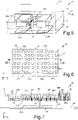
- the accelerometer described in the above papers has a rectangular shaped mobile mass 31 hinged to a pillar 33 in a median position, as may be seen in particular in the top plan view of Figure 6 , where the rotation axis is designated by 01 and extends parallel to the shorter sides of the rectangle, equidistant from them.
- the mobile mass 31 is formed by a platform of semiconductor material, comprising two half-masses 32A, 32B having a plurality of through holes 34.
- the through holes 34 have the same area in a plane parallel to plane XY of a Cartesian reference system XYZ and present an arrangement symmetrical with respect to the rotation axis 01.
- each half-mass 32A, 32B comprises a first portion 35A, respectively 35B, contiguous to the rotation axis 01 and a second portion 36A, 36B arranged more remotely from the rotation axis 01, as a prolongation of the respective first portion 35A, 35B.
- the first portions 35A, 35B are identical to each other and in particular have the same area in a plane parallel to the plane XY (as may be noted in Figure 6 ) and the same thickness along axis Z (as may be noted in Figure 7 , showing a cross-section view parallel to plane XY of the Cartesian reference system XYZ).
- the second portions 36A, 36B have the same area but a different thickness along axis Z: the second portion 36A of the first half-mass 32A (on the left in Figures 5 to 7 ) has a smaller thickness than the second portion 36B of the second half-mass 32B (on the right in Figures 5 to 7 ).
- the second portion 36A of the first half-mass 32A has the same thickness as the first portions 35A, 35B, and the second portion 36B of the second half-mass 32B has a larger thickness.
- Figure 7 shows the forces acting on the half-masses 32A and 32B in presence of a temperature gradient within the mobile mass 31, with hot air molecules moving from below upwards (as represented by the arrows 46, in darker grey in the hotter areas, at the top, and lighter grey in the colder areas, at the bottom).
- a first and a second radiometric force F1, F2 act on the first and the second half-masses 32A, 32B and are different from each other, because of the different thicknesses of the two half-masses 32A, 32B.
- the radiometric effect creates a non-negligible twisting moment that leads to offset deviations in the output signal of the accelerometer.
- the aim of the present invention is to provide a MEMS sensor that overcomes the drawbacks of the prior art.
- FIGS 8 and 9 are schematic illustrations of a sensor 50 of an inertial type having a so-called “teeter-totter” structure.
- the senor 50 comprises a mobile mass 51 suspended over a substrate 52 ( Figure 9 ) through a pillar 53, which extends from the substrate 52 parallel to axis Z of a Cartesian reference system XYZ.
- the pillar 53 is coupled to the mobile mass 51 through hinges and springs (not shown), which enable tilting of the mobile mass 51 about a rotation axis A.
- the mobile mass 51 has a characteristic quantity (here the length in direction X) much greater than its thickness, for example ten times greater.
- the mobile mass 51 has main surfaces (top surface 51A and bottom surface 51B) extending in a plane parallel to plane XY of the Cartesian reference system XYZ and a thickness t p extending parallel to axis Z.
- the thickness t p of the mobile mass 51 is uniform over its entire area, as may be seen in Figure 9 .
- the mobile mass 51 has (in top plan view) a generally rectangular shape with sides parallel to axes X and Y, and the rotation axis A (which extends parallel to axis Y) is eccentric with respect to the rectangular shape of the mobile mass 51.
- the rotation axis A divides the mobile mass 51 into a first half-mass 54 and a second half-mass 55, which are arranged on opposite sides with respect to the rotation axis A and have different areas.
- the first and the second half-masses 54, 55 thus each have an own centroid B1, B2 arranged at a first distance b1 and a second distance b2, respectively, different from each other, from the rotation axis A, as shown in Figure 9 .
- a first and a second electrode 56, 57 are arranged in front of the bottom surface 51B, facing the first and the second half-mass 54, 55, respectively, and form therewith a first and a second capacitive element 58, 59, respectively.
- the half-masses 54, 55 are perforated in a non-uniform way; in particular, the first half-mass 54 has first holes 60, and the second half-mass 61 has second holes 61.
- the first perimeter p1 is given by the sum of all the perimeters of the first holes 60 and of the outer perimeter of the half-mass 54
- the second perimeter p2 is given by the sum of all the perimeters of the second holes 61 and of the outer perimeter of the half-mass 55.
- Eq. (2) becomes (the quantities being indexed by 1 or 2 according to whether they refer to the first or the second mass 54, 55 or being without index, if they are the same for both masses)
- F 1 ⁇ 1 2 P c ⁇ 0 2 T 0 P 0 P c 2 T h ⁇ T c t p p 1
- F 2 ⁇ 1 2 P c ⁇ 0 2 T 0 P 0 P c 2 T h ⁇ T c t p p 2
- moments M1, M2 of equal value act on the first and on the second mass 54, 55, respectively, and compensate each other. It follows that, with the indicated geometrical conditions, the radiometric forces act on the mobile mass 51, but do not cause rotation of the mobile mass 51 and thus do not give rise to an offset signal.
- FIG. 10 An embodiment of an accelerometer that satisfies above condition (3) or (3.1) and thus has a compensated radiometric effect is shown in Figure 10 , where, for simplicity, parts equivalent to those of the sensor 50 of Figures 8 and 9 are designated by numbers increased by 100 and are not described in detail.
- the accelerometer 150 of Figure 10 comprises a suspended mass 151 (wherein only half of the structure is shown; the entire structure of the suspended mass 151 may be obtained by turning over the structure shown in Figure 10 about the horizontal axis B).
- the suspended mass 151 has a first half-mass 154 and a second half-mass 155, carried by a plurality of pillars 153 (in the shown embodiment, four pillars 153, two whereof are visible).
- a spring 170 connects the pillars 153 to the two half-masses 154, 155 (a similar spring, not shown, is obviously provided in the mobile half-mass 151, not shown) .
- the spring 170 has a broken-line structure, with a pair of first portions 170A (which extend from and about the respective pillars 153), a single central portion 170B (which is a prolongation of the first portions and extends along the rotation axis A), and two divergent portions 170C (which extend from the central portion 170B towards a respective half-mass 154, 155, perpendicularly to the rotation axis A).
- the shape of the spring 170 may vary and is not part of the present patent application.
- each half-mass 154, 155 has a plurality of openings, not symmetrical to the rotation axis A, the number and sizes whereof satisfy the relation of Eq. (3) or Eq. (3.1) referred to above.
- the half-mass 154 which has a smaller area, has dampening openings 175 accommodating a plurality of dampening structures 176 (two whereof are shown in Figure 10 ), which are not part of the present patent application.
- the first half-mass 154 has a delimitation side 177, generally parallel to the rotation axis A, having a projection 178 accommodating rectangular openings 179.
- Further openings 180 may extend in the first half-mass 154, asymmetrical with respect to the second half-mass 155.
- the dampening openings 175, the rectangular openings 179, and the further openings 180, all through openings are studied so that the sum of their perimeters, together with the perimeters of the first holes 160, of the first half-mass 154, and of the half-trench of the spring 170, satisfies the relation, given by Eq. (3), with respect to the sum of the perimeters of the second holes 161, of the second half-mass 155, and of the other half-trench of the spring 170.
- Figure 11A and 11B represent hysteresis measurements performed on devices with similar structures, initially re-heated on one side from -80°C up to approximately 60°C and then cooled from approximately 60°C down to -80°C.
- Figure 11A shows the acceleration (in mg, where g is the acceleration of gravity) obtained with a traditional accelerometer having through openings linked only to usual geometrical and functional considerations and not satisfying relation (3) set forth above
- Figure 11B shows the results obtained with the device of Figure 10 and differing from the traditional accelerometer only as regards the geometry of the through openings.
- the above result may be obtained by varying just the geometry and the perimeter of the openings, holes, and through trenches in the first half-mass 54 (i.e., the smaller size half-mass of Figure 8 ); however, the modification of the through openings for satisfying relation (3) may also regard just the second half-mass 55 (of larger sizes).
- this condition maybe obtained without impact on the electromechanical parameters, the dimensions, and the mechanical strength of the mobile mass, and thus without impact on other performance parameters of the inertial sensor, while improving the behaviour in regard to radiometric forces.
- the sought sizing may be obtained without modification of the manufacturing process of the inertial sensor, and thus at unvaried manufacturing costs.
- the described inertial sensor is particularly adapted to integration in an electronic device 200, as shown in Figure 12 , which may be used in a plurality of electronic systems intended for processing, storing, transmitting, and receiving signals and information.
- the electronic device 200 may be, for example, an inertial navigation system, an automotive system, or a portable system, such as a PDA (Personal Digital Assistant), a portable computer, a mobile phone, a wearable device, such as a smartwatch, a digital audio player, a photographic camera or a video camera.
- PDA Personal Digital Assistant
- the electronic device 200 may, for example, comprise the sensor 50, here forming an accelerometer; an electronic circuit 205, typically an ASIC, operatively coupled to the sensor 50, forming a reading interface for the sensor 50, supplying biasing signals to the sensor 50 (in a per se known manner, here not shown in detail), detecting the displacement degree of the mobile mass 51 ( Figure 8 ), and thus determining acceleration along Z acting on the mobile mass 51; and an electronic control unit 220, for example a microprocessor, connected to the electronic circuit 205 and configured to supervise general operation of the electronic device 200, for example on the basis of the detected accelerations.
- an electronic control unit 220 for example a microprocessor
- the electronic apparatus 200 may comprise an input/output interface 240, for example having a keyboard and a display, connected to the electronic control unit 220, a speaker 250, for generating sounds on an audio output (not shown), and an internal memory 260.
- the sensor 50 and the electronic circuit 205 may be packaged in a packaging structure and form an inertial device 230.
Description
- The present invention relates to a MEMS device with optimised geometry for reducing offset due to the radiometric effect. In particular, the present invention relates to a MEMS (Micro-Electro-Mechanical System) inertial sensor, such as an accelerometer or a gyroscope, having so-called "teeter-totter" structure, wherein a suspended mass is tiltable about a horizontal rotation axis belonging to the plane of extension of the suspended mass and extending therethrough so that the two parts of the suspended mass arranged on opposite sides of the rotation axis move in opposite directions, transversal to the plane of extension (the so-called out-of-plane movement or Z movement).
- As is known, the use of MEMS devices of the above type is progressively increasing in ever-wider technical fields, due to their capacity of supplying accurate signals, their low cost, and their high versatility.
-
US 2009/031809 discloses a symmetrical differential capacitive sensor having a movable element pivotable about a geometrically centered rotational axis and formed by two sections with different configurations of apertures. -
EP 2 151 691 - In particular, inertial sensors of the above type are progressively used in consumer applications and in the automotive field, for example for indoor navigation and as aids to autonomous driving, i.e., applications where it is important to have a high precision and provide outputs as stable as possible also when the environmental and/or internal parameters vary. In particular, in these applications, it is desirable for the output signals of the device to be stable in temperature, both with respect to external effects, which operate in a uniform way over the entire die integrating the device, and with respect to internal effects, operating in different ways within the die. To take into account the external effects, many MEMS devices have arrangements for compensating signal variations due to the external temperature. As regards the internal effects, the problem has only recently been recognised and tackled, as discussed hereinafter.
- In general, non-uniform temperature distributions within a MEMS device of the above type have various grounds. A first ground is linked to the high integration density of electronic devices in complex apparatuses; other grounds may be linked to contingent situations.
- For instance,
Figure 1 shows an exemplar situation in which a printed-circuit board 1 carries twoMEMS devices 2 of an inertial type, arranged one above and one beneath the printed-circuit board 1, and a processing device (CPU) 3. In some applications, the printed-circuit board 1 may carry just one MEMS device or a plurality of MEMS devices or other integrated devices, arranged alongside each other also in planes extending before or behind of the sheet plane, on just one side or on both sides of the printed-circuit board 1, in a not shown manner. In this situation, the small distance and the high number of energy dissipating devices at a short distance on one side of the considered MEMS device or on the opposite surface of the printed-circuit board 1 may give rise to temperature profiles variable in a horizontal or vertical direction (with reference to the sheet plane). - Other causes of non-uniform temperature distributions are linked to operating considerations. In fact, In some situations, for example at turning-on of the device, fast temperature variations may lead to a non-uniform distribution within the die, as represented in
Figure 2 . Here asensor 5 comprises aMEMS device 6, carried by a printed-circuit board 7 and, in turn, carrying an integrateddevice 8 such as an ASIC (Application-Specific Integrated Circuit). In this case, at least in some operating conditions, there is a non-constant temperature profile in a vertical direction as a result of the integrateddevice 7, which, during its operation, emits heat. In this situation, theMEMS device 6 may have a variable temperature profile, and precisely decreasing from a high value on the top face of theMEMS device 6 to a lower value on the bottom face of theMEMS device 6. - It has been demonstrated that a temperature gradient along axis Z (out-of-plane direction) in a sensor mobile in this direction causes a static deviation of the offset of the output signal representing the movement along axis Z, whereas the output signals representing movements along the other axes X and Y are not affected by this phenomenon. This situation is represented in
Figures 3 and 4 , which are schematic illustrations of an inertial sensor having "teeter-totter" structure. - In detail,
Figures 3 and 4 show aMEMS accelerometer 10 formed by amobile mass 11 having atop surface 11A and abottom surface 11B and suspended over asubstrate 12. Themobile mass 11 is roughly formed by a platform or plate having a main extension in a plane that, at rest, is parallel to plane XY of a Cartesian reference system XYZ. Themobile mass 11 may, for example, have (in top plan view) a generally rectangular shape and is carried by apillar 13 extending from thesubstrate 12 parallel to axis Z of the Cartesian reference system XYZ. Thepillar 13 is coupled to themobile mass 11 via hinges and springs (not shown) allowing rotation of themobile mass 11 about arotation axis 0 parallel to axis Y extending through themobile mass 11. - In particular, in these devices, the
rotation axis 0 is eccentric and is spaced from the centroid (not shown) of themobile mass 11 and divides themobile mass 11 into a first half-mass 14A and a second half-mass 14B, arranged on opposite sides with respect to therotation axis 0. The first and the second half-masses rotation axis 0. In the example shown, the first half-mass 14A has a size smaller than the second half-mass 14B. - A first and a
second electrode masses bottom surface 11B of the mobile mass 11). In detail, the first and asecond electrode masses capacitive element -
Figure 3 shows the ideal situation in absence of (internal or external) forces acting on themobile mass 11. In this situation, themobile mass 11 is in a resting position, and its main extension plane is parallel to plane XY, as mentioned above. In this situation, the first and the second half-masses respective electrode capacitive elements capacitive elements - In
Figure 4 , ahot source 21 has been arranged above themobile mass 11 facing thetop surface 11A, and acold source 22 has been arranged underneath themobile mass 11 facing thebottom surface 11B. - The
sources mobile mass 11 in a direction parallel to axis Z. In this situation, even with no applied external forces, themobile mass 11 turns, here in a clockwise direction (arrow 25). Consequently, thecapacitive elements - Rotation of the
mobile mass 11 with an internal temperature gradient is caused by radiometric effects. These effects, discovered in 1873 by William Crookes and exploited in the Crookes radiometer (also known as "light mill") are linked to the action exerted by gas molecules acting in a differential way on opposite surfaces, heated at different temperatures. In particular, according to Einstein's radiometric theory, the radiometric forces depend upon the mean free path λ of the molecules of the gas in which the considered body (MEMS device 10) is immersed; the mean free path, in turn, depends upon the gas density and the molecule section. The radiometric forces moreover depend upon the value and direction of the temperature gradient and, for a plate-shaped structure having a cavity, follow the law:
F2p is the force acting on the structure;
P0 is the standard pressure (1 bar);
Pc is the pressure in the cavity;
λ is the mean free path of the gas molecules at pressure Pc
λ 0 is the mean free path of the gas molecules at pressure P0
T0 is the standard temperature (25°C);
L is the perimeter of the cavity; and

- Assuming that the temperature variation depends only upon space and due to the small thickness of the plate-shaped structure, we have:

Eq. (1) thus becomes:
- The problem of the radiometric forces acting on a mobile mass (having a flat shape) of a MEMS device has so far not been tackled very much. A solution is described in the papers "ADVANCED SURFACE MICROMACHINING PROCESS - A FIRST STEP TOWARDS 3D MEMS" by J. Classen et al., MEMS 2017, Las Vegas, NV, USA, January 22-26, 2017, IEEE, 978-1-5090-5078-9/17 and "Radiometric effects in MEMS Accelerometers", by C. Nagel et al., IEEE, 978-1-5090-1012-7/17, which describe an accelerometer configured to detect forces acting in direction Z (out of the plane of the mobile platform) having a symmetrical structure, shown in
Figures 5 to 7 . - In detail, the accelerometer described in the above papers (designated by 30 in
Figures 5 to 7 ) has a rectangular shapedmobile mass 31 hinged to apillar 33 in a median position, as may be seen in particular in the top plan view ofFigure 6 , where the rotation axis is designated by 01 and extends parallel to the shorter sides of the rectangle, equidistant from them. Themobile mass 31 is formed by a platform of semiconductor material, comprising two half-masses holes 34. As may be seen, in particular, inFigure 6 , the throughholes 34 have the same area in a plane parallel to plane XY of a Cartesian reference system XYZ and present an arrangement symmetrical with respect to therotation axis 01. - As may be noted, in particular, in the cross-section of
Figure 7 , each half-mass first portion 35A, respectively 35B, contiguous to therotation axis 01 and asecond portion rotation axis 01, as a prolongation of the respectivefirst portion - The
first portions Figure 6 ) and the same thickness along axis Z (as may be noted inFigure 7 , showing a cross-section view parallel to plane XY of the Cartesian reference system XYZ). Thesecond portions second portion 36A of the first half-mass 32A (on the left inFigures 5 to 7 ) has a smaller thickness than thesecond portion 36B of the second half-mass 32B (on the right inFigures 5 to 7 ). In particular, in the example shown, thesecond portion 36A of the first half-mass 32A has the same thickness as thefirst portions second portion 36B of the second half-mass 32B has a larger thickness. - A
substrate 44,top electrodes bottom electrodes 41A, 42B (carried by the substrate 44), together with acap 43 complete the structure of theaccelerometer 30. -
Figure 7 shows the forces acting on the half-masses mobile mass 31, with hot air molecules moving from below upwards (as represented by the arrows 46, in darker grey in the hotter areas, at the top, and lighter grey in the colder areas, at the bottom). - In this situation, on the hypothesis that the thicknesses of the
portions masses Figure 7 ) act on the first and the second half-masses masses masses rotation axis 01 and thus the same application arm of the forces F1, F2, it is possible to demonstrate that the ratio between the moments acting on the half-masses - Consequently, different moments act on the two half-
masses mobile mass 31, in the considered example (with the temperature of the top surface of themobile mass 31 higher than on the bottom surface) in a clockwise direction. - It follows that, also with this known structure, the radiometric effect creates a non-negligible twisting moment that leads to offset deviations in the output signal of the accelerometer.
- The aim of the present invention is to provide a MEMS sensor that overcomes the drawbacks of the prior art.
- According to the present invention a MEMS device is provided, as defined in the attached claims.
- For a better understanding of the present invention, embodiments thereof are now described, purely by way of nonlimiting example, with reference to the attached drawings, wherein:
-
Figure 1 is a schematic illustration of a system comprising a plurality of MEMS sensors and the corresponding electronic unit on a printed-circuit board; -
Figure 2 is a schematic illustration of another MEMS sensor with different arrangement of the sensor and of the electronic unit; -
Figure 3 is a schematic side view of a MEMS sensor of a "teeter-totter" type in a resting condition and in absence of stresses; -
Figure 4 is a schematic side view of a MEMS sensor of a "teeter-totter" type in presence of stresses due to the radiometric effect; -
Figure 5 is a simplified perspective view of a known accelerometer; -
Figure 6 is a top plan view of the accelerometer ofFigure 5 ; -
Figure 7 is a schematic longitudinal section, taken along the section plane VII-VII ofFigure 6 , representing the acting forces caused by the radiometric effect; -
Figure 8 is a schematic top plan view of the layout of the mobile mass according to an embodiment of the present device; -
Figure 9 is a schematic longitudinal section, taken along the section plane IX-IX ofFigure 8 of the present device; -
Figure 10 is a top plan view of a possible embodiment of the present device; -
Figures 11A and 11B show the results of measurements made on a known device and on the device ofFigure 10 ; and -
Figure 12 shows a general block diagram of an electronic device incorporating the present device. -
Figures 8 and 9 are schematic illustrations of asensor 50 of an inertial type having a so-called "teeter-totter" structure. - In detail, the
sensor 50 comprises amobile mass 51 suspended over a substrate 52 (Figure 9 ) through apillar 53, which extends from thesubstrate 52 parallel to axis Z of a Cartesian reference system XYZ. Thepillar 53 is coupled to themobile mass 51 through hinges and springs (not shown), which enable tilting of themobile mass 51 about a rotation axis A. - The
mobile mass 51 has a characteristic quantity (here the length in direction X) much greater than its thickness, for example ten times greater. In particular, at rest, themobile mass 51 has main surfaces (top surface 51A andbottom surface 51B) extending in a plane parallel to plane XY of the Cartesian reference system XYZ and a thickness tp extending parallel to axis Z. The thickness tp of themobile mass 51 is uniform over its entire area, as may be seen inFigure 9 . In the shown example, themobile mass 51 has (in top plan view) a generally rectangular shape with sides parallel to axes X and Y, and the rotation axis A (which extends parallel to axis Y) is eccentric with respect to the rectangular shape of themobile mass 51. Consequently, the rotation axis A divides themobile mass 51 into a first half-mass 54 and a second half-mass 55, which are arranged on opposite sides with respect to the rotation axis A and have different areas. The first and the second half-masses Figure 9 . In particular, in thedevice 50 shown inFigures 8 and 9 , b1 < b2. - A first and a
second electrode bottom surface 51B, facing the first and the second half-mass second capacitive element - The half-
masses mass 54 has first holes 60, and the second half-mass 61 has second holes 61. - The
first holes 60 and thesecond holes 61 are provided in a number and have dimensions such as to globally define (together with the corresponding half-masses 54, 55) a first perimeter p1 and a second perimeter p2 different from each other, with p1 > p2, and such as to satisfy the following equation:
- In particular, in Eq. (3) above, the first perimeter p1 is given by the sum of all the perimeters of the
first holes 60 and of the outer perimeter of the half-mass 54, and, likewise, the second perimeter p2 is given by the sum of all the perimeters of thesecond holes 61 and of the outer perimeter of the half-mass 55. - In
Figure 8 , this is represented by formingfirst holes 60 that are different in number from thesecond holes 61 and have a rectangular shape, with length W1 of the shorter side and length L1 of the longer side, whereas thesecond holes 61 have a square shape, with side L2 > L1. However, the combinations of number, shape, and arrangement of theholes 61, 62 is infinite, and the only condition to be satisfied, to minimise the drift due to the radiometric effect, is Eq. (3) . - For instance, the
second holes 61 may also have a rectangular shape with length W2 of the shorter side and length L2 of the longer side. Consequently, in general, and on the hypothesis of having first andsecond holes 
first holes 60, and N2 is the number ofsecond holes 61. - In this situation, Eq. (2) becomes (the quantities being indexed by 1 or 2 according to whether they refer to the first or the
second mass 

- Moreover, the moments M1 and M2 acting on the first and the
second masses 

- Combining Eqs. (2.1), (2.2), (4.1) and (4.2) and taking into account Eq. (3), we obtain

- Thus, moments M1, M2 of equal value act on the first and on the
second mass mobile mass 51, but do not cause rotation of themobile mass 51 and thus do not give rise to an offset signal. - An embodiment of an accelerometer that satisfies above condition (3) or (3.1) and thus has a compensated radiometric effect is shown in
Figure 10 , where, for simplicity, parts equivalent to those of thesensor 50 ofFigures 8 and 9 are designated by numbers increased by 100 and are not described in detail. - In particular, the
accelerometer 150 ofFigure 10 comprises a suspended mass 151 (wherein only half of the structure is shown; the entire structure of the suspendedmass 151 may be obtained by turning over the structure shown inFigure 10 about the horizontal axis B). - The suspended
mass 151 has a first half-mass 154 and a second half-mass 155, carried by a plurality of pillars 153 (in the shown embodiment, fourpillars 153, two whereof are visible). InFigure 10 , aspring 170 connects thepillars 153 to the two half-masses 154, 155 (a similar spring, not shown, is obviously provided in the mobile half-mass 151, not shown) . In the embodiment shown, thespring 170 has a broken-line structure, with a pair offirst portions 170A (which extend from and about the respective pillars 153), a singlecentral portion 170B (which is a prolongation of the first portions and extends along the rotation axis A), and twodivergent portions 170C (which extend from thecentral portion 170B towards a respective half-mass spring 170 may vary and is not part of the present patent application. - According to the above, each half-
mass - In the embodiment shown, the half-
mass 154, which has a smaller area, has dampeningopenings 175 accommodating a plurality of dampening structures 176 (two whereof are shown inFigure 10 ), which are not part of the present patent application. - Moreover, in the embodiment shown, the first half-
mass 154 has adelimitation side 177, generally parallel to the rotation axis A, having aprojection 178 accommodatingrectangular openings 179. -
Further openings 180 may extend in the first half-mass 154, asymmetrical with respect to the second half-mass 155. - In the
accelerometer 150, the dampeningopenings 175, therectangular openings 179, and thefurther openings 180, all through openings, are studied so that the sum of their perimeters, together with the perimeters of thefirst holes 160, of the first half-mass 154, and of the half-trench of thespring 170, satisfies the relation, given by Eq. (3), with respect to the sum of the perimeters of thesecond holes 161, of the second half-mass 155, and of the other half-trench of thespring 170. - Thereby, by a simple sizing in the design stage, it is possible to drastically reduce or even cancel altogether the offset of the output signal due to the radiometric effect, in absence of other stresses.
- Studies conducted by the applicant have confirmed the theoretical results, as shown in
Figures 11A and 11B , which represent hysteresis measurements performed on devices with similar structures, initially re-heated on one side from -80°C up to approximately 60°C and then cooled from approximately 60°C down to -80°C. In particular,Figure 11A shows the acceleration (in mg, where g is the acceleration of gravity) obtained with a traditional accelerometer having through openings linked only to usual geometrical and functional considerations and not satisfying relation (3) set forth above, andFigure 11B shows the results obtained with the device ofFigure 10 and differing from the traditional accelerometer only as regards the geometry of the through openings. As may be noted, in the traditional device (Figure 11A ), the heating and cooling curves show high hysteresis, whereas in the device satisfying condition (3) (Figure 11B ), the heating and cooling curves are practically superimposed and there is practically no hysteresis. - The above result may be obtained by varying just the geometry and the perimeter of the openings, holes, and through trenches in the first half-mass 54 (i.e., the smaller size half-mass of
Figure 8 ); however, the modification of the through openings for satisfying relation (3) may also regard just the second half-mass 55 (of larger sizes). Advantageously, this condition maybe obtained without impact on the electromechanical parameters, the dimensions, and the mechanical strength of the mobile mass, and thus without impact on other performance parameters of the inertial sensor, while improving the behaviour in regard to radiometric forces. - Moreover, the sought sizing may be obtained without modification of the manufacturing process of the inertial sensor, and thus at unvaried manufacturing costs.
- The described inertial sensor is particularly adapted to integration in an
electronic device 200, as shown inFigure 12 , which may be used in a plurality of electronic systems intended for processing, storing, transmitting, and receiving signals and information. For instance, theelectronic device 200 may be, for example, an inertial navigation system, an automotive system, or a portable system, such as a PDA (Personal Digital Assistant), a portable computer, a mobile phone, a wearable device, such as a smartwatch, a digital audio player, a photographic camera or a video camera. - The
electronic device 200 may, for example, comprise thesensor 50, here forming an accelerometer; anelectronic circuit 205, typically an ASIC, operatively coupled to thesensor 50, forming a reading interface for thesensor 50, supplying biasing signals to the sensor 50 (in a per se known manner, here not shown in detail), detecting the displacement degree of the mobile mass 51 (Figure 8 ), and thus determining acceleration along Z acting on themobile mass 51; and anelectronic control unit 220, for example a microprocessor, connected to theelectronic circuit 205 and configured to supervise general operation of theelectronic device 200, for example on the basis of the detected accelerations. Moreover, theelectronic apparatus 200 may comprise an input/output interface 240, for example having a keyboard and a display, connected to theelectronic control unit 220, aspeaker 250, for generating sounds on an audio output (not shown), and aninternal memory 260. Thesensor 50 and theelectronic circuit 205 may be packaged in a packaging structure and form aninertial device 230. - Finally, it is clear that modifications and variations may be made to the MEMS device described and shown herein, without thereby departing from the scope of the present invention, as defined in the attached claims. In particular, as has been mentioned, the arrangement and number of through openings may vary widely with respect to what has been shown and also the shape and arrangement of the mobile mass and of the structures envisaged may be any, linked to the respective functions, with the condition that the openings satisfy the relation (3) above.
Claims (8)
- A MEMS device (50; 150) with a teeter-totter structure, comprising:a mobile mass (51; 151) having an area in a plane and a thickness in a direction perpendicular to the plane, the mobile mass being tiltable about a rotation axis (A) extending parallel to the plane and formed by a first anda second half-mass (54, 55; 154, 155), arranged on opposite sides of the rotation axis, the first and the second half-masses having a first and a second centroid (B1, B2), respectively, arranged at a first and a second distance b1, b2, respectively, from the rotation axis;first through openings (60; 160, 175, 179, 180) in the first half-mass (54; 154), the sum of all the perimeters of the first through openings and of the outer perimeter of the first half-mass defining a first total perimeter p1 in the plane; andsecond through openings (61; 161) in the second half-mass (55; 155), the sum of all the perimeters of the second through openings and of the outer perimeter of the second half-mass defininga second total perimeter p2 in the plane, characterized in that the MEMS device is designed such that the first and the second perimeters p1, p2 and the first and second distances b1, b2 satisfy equation:

- The MEMS device according to claim 1, forming an accelerometer or a gyroscope.
- The MEMS device according to claim 1 or 2, forming a Z-axis accelerometer.
- The device according to any of the preceding claims, wherein the mobile mass (51; 151) comprises a monolithic semiconductor platform.
- The device according to any of the preceding claims, wherein the mobile mass (51; 151) has a uniform thickness.
- The device according to any of the preceding claims, wherein the number of second through openings (61; 161) is different from the number of first through openings (60; 160, 175, 179, 180).
- The device according to any of the preceding claims, wherein the shape of the second through openings (61; 161) is different from the shape of the first through openings (60; 160, 175, 179, 180).
- An electronic apparatus (200) comprising:the MEMS device (50; 150) according to any of the preceding claims;an electronic circuit (205) coupled to the MEMS device;a processing unit (220), coupled to the electronic circuit (205);an interface (240) coupled to the processing unit (220); anda storage device (260) coupled to the processing unit (220) .
Applications Claiming Priority (1)
| Application Number | Priority Date | Filing Date | Title |
|---|---|---|---|
| IT102019000000190A IT201900000190A1 (en) | 2019-01-08 | 2019-01-08 | MEMS DEVICE WITH OPTIMIZED GEOMETRY FOR REDUCING THE OFFSET DUE TO THE RADIOMETRIC EFFECT |
Publications (2)
| Publication Number | Publication Date |
|---|---|
| EP3680671A1 EP3680671A1 (en) | 2020-07-15 |
| EP3680671B1 true EP3680671B1 (en) | 2022-06-01 |
Family
ID=65952011
Family Applications (1)
| Application Number | Title | Priority Date | Filing Date |
|---|---|---|---|
| EP19220232.3A Active EP3680671B1 (en) | 2019-01-08 | 2019-12-31 | Mems device with optimized geometry for reducing the offset due to the radiometric effect |
Country Status (4)
| Country | Link |
|---|---|
| US (1) | US11603310B2 (en) |
| EP (1) | EP3680671B1 (en) |
| CN (2) | CN111410167A (en) |
| IT (1) | IT201900000190A1 (en) |
Families Citing this family (6)
| Publication number | Priority date | Publication date | Assignee | Title |
|---|---|---|---|---|
| FR3114583B1 (en) * | 2020-09-29 | 2022-09-16 | Commissariat Energie Atomique | METHOD FOR MANUFACTURING AN ELECTROACOUSTIC TRANSDUCER |
| CN112151312B (en) * | 2020-10-13 | 2023-04-07 | 深圳清华大学研究院 | Electrode switch based on structure is super smooth |
| JP2022071262A (en) * | 2020-10-28 | 2022-05-16 | セイコーエプソン株式会社 | Physical quantity sensor, physical quantity sensor device, and inertial measurement device |
| US11609091B2 (en) * | 2020-11-16 | 2023-03-21 | Knowles Electronics, Llc | Microelectromechanical systems device including a proof mass and movable plate |
| DE102021204615A1 (en) | 2021-05-06 | 2022-11-10 | Robert Bosch Gesellschaft mit beschränkter Haftung | Method for temperature compensation of a microelectromechanical sensor and microelectromechanical sensor |
| CN114280331A (en) * | 2021-12-16 | 2022-04-05 | 宁波奥拉半导体有限公司 | Z-axis accelerometer |
Family Cites Families (18)
| Publication number | Priority date | Publication date | Assignee | Title |
|---|---|---|---|---|
| US7121141B2 (en) * | 2005-01-28 | 2006-10-17 | Freescale Semiconductor, Inc. | Z-axis accelerometer with at least two gap sizes and travel stops disposed outside an active capacitor area |
| US7140250B2 (en) * | 2005-02-18 | 2006-11-28 | Honeywell International Inc. | MEMS teeter-totter accelerometer having reduced non-linearty |
| DE102006058747A1 (en) * | 2006-12-12 | 2008-06-19 | Robert Bosch Gmbh | Micromechanical z-sensor |
| US7578190B2 (en) * | 2007-08-03 | 2009-08-25 | Freescale Semiconductor, Inc. | Symmetrical differential capacitive sensor and method of making same |
| US8171793B2 (en) * | 2008-07-31 | 2012-05-08 | Honeywell International Inc. | Systems and methods for detecting out-of-plane linear acceleration with a closed loop linear drive accelerometer |
| DE102008043788A1 (en) * | 2008-11-17 | 2010-05-20 | Robert Bosch Gmbh | Micromechanical component |
| DE102009000167A1 (en) * | 2009-01-13 | 2010-07-22 | Robert Bosch Gmbh | sensor arrangement |
| DE102009029248B4 (en) * | 2009-09-08 | 2022-12-15 | Robert Bosch Gmbh | Micromechanical system for detecting an acceleration |
| JP5790296B2 (en) * | 2011-08-17 | 2015-10-07 | セイコーエプソン株式会社 | Physical quantity sensor and electronic equipment |
| JP5935986B2 (en) * | 2012-04-06 | 2016-06-15 | セイコーエプソン株式会社 | Physical quantity sensor and electronic equipment |
| JP2015072188A (en) * | 2013-10-03 | 2015-04-16 | セイコーエプソン株式会社 | Physical quantity detection element, physical quantity detection device, electronic apparatus and moving body |
| JP6401868B2 (en) * | 2015-09-15 | 2018-10-10 | 株式会社日立製作所 | Acceleration sensor |
| JP6401728B2 (en) * | 2016-03-18 | 2018-10-10 | 株式会社日立製作所 | Inertial sensor and manufacturing method thereof |
| JP2019045170A (en) * | 2017-08-30 | 2019-03-22 | セイコーエプソン株式会社 | Physical quantity sensor, composite sensor, inertial measurement unit, portable electronic equipment, electronic equipment, and mobile body |
| JP2019045172A (en) * | 2017-08-30 | 2019-03-22 | セイコーエプソン株式会社 | Physical quantity sensor, composite sensor, inertial measurement unit, portable electronic equipment, electronic equipment, and mobile body |
| DE102018209500B4 (en) * | 2018-06-14 | 2020-10-08 | Robert Bosch Gmbh | Micromechanical z-inertial sensor |
| DE102018213746A1 (en) * | 2018-08-15 | 2020-02-20 | Robert Bosch Gmbh | Micromechanical inertial sensor |
| DE102018219546B3 (en) * | 2018-11-15 | 2019-09-12 | Robert Bosch Gmbh | Micromechanical component |
-
2019
- 2019-01-08 IT IT102019000000190A patent/IT201900000190A1/en unknown
- 2019-12-31 EP EP19220232.3A patent/EP3680671B1/en active Active
-
2020
- 2020-01-07 US US16/736,485 patent/US11603310B2/en active Active
- 2020-01-07 CN CN202010015562.9A patent/CN111410167A/en active Pending
- 2020-01-07 CN CN202020027496.2U patent/CN211896030U/en active Active
Also Published As
| Publication number | Publication date |
|---|---|
| US20200216305A1 (en) | 2020-07-09 |
| IT201900000190A1 (en) | 2020-07-08 |
| CN111410167A (en) | 2020-07-14 |
| US11603310B2 (en) | 2023-03-14 |
| EP3680671A1 (en) | 2020-07-15 |
| CN211896030U (en) | 2020-11-10 |
Similar Documents
| Publication | Publication Date | Title |
|---|---|---|
| EP3680671B1 (en) | Mems device with optimized geometry for reducing the offset due to the radiometric effect | |
| EP2703824B1 (en) | MEMS accelerometer comprising pendulous masses being pivotable in the substrate plane | |
| CN108020687B (en) | MEMS accelerometer | |
| EP2893362B1 (en) | Dual and triple axis inertial sensors and methods of inertial sensing | |
| EP1738181B1 (en) | Out-of-plane compensation electrode suspension for an accelerometer | |
| US9327962B2 (en) | MEMS device and corresponding micromechanical structure with integrated compensation of thermo-mechanical stress | |
| US7093478B2 (en) | Method for calibrating accelerometer sensitivity | |
| ITTO20130237A1 (en) | HIGH SENSITIVITY MICROELECTROMECHANICAL DETECTION OF Z AXIS, IN PARTICULAR FOR A MEMS ACCELEROMETER | |
| EP3186664B1 (en) | Measurement of acceleration | |
| TWI616656B (en) | A mems sensor and a semiconductor package | |
| EP1691202A1 (en) | Vibration piezoelectric acceleration sensor | |
| Zhou et al. | Analytical study of temperature coefficients of bulk MEMS capacitive accelerometers operating in closed-loop mode | |
| EP4187258A1 (en) | Z-axis microelectromechanical sensor device with improved stress insensitivity | |
| Khamil et al. | Analysis of mems accelerometer for optimized sensitivity | |
| Serrano-Vázquez et al. | Design and modeling of a single-mass biaxial capacitive accelerometer based on the SUMMiT V process | |
| KR100771167B1 (en) | micromachined convective accelerometer | |
| Joshi et al. | Optimising performance of a cantilever-type micro accelerometer sensor | |
| Upadhyay et al. | Design, Simulation and Fabrication of MEMS-based Piezoresistive Accelerometer | |
| KR100252696B1 (en) | Micro accelerometer | |
| CN112730890A (en) | Acceleration sensor and electronic device | |
| JP3036681B2 (en) | Capacitive acceleration sensor | |
| Joshi et al. | Performance optimization of a cantilever-type micro-accelerometer |
Legal Events
| Date | Code | Title | Description |
|---|---|---|---|
| PUAI | Public reference made under article 153(3) epc to a published international application that has entered the european phase |
Free format text: ORIGINAL CODE: 0009012 |
|
| STAA | Information on the status of an ep patent application or granted ep patent |
Free format text: STATUS: THE APPLICATION HAS BEEN PUBLISHED |
|
| AK | Designated contracting states |
Kind code of ref document: A1 Designated state(s): AL AT BE BG CH CY CZ DE DK EE ES FI FR GB GR HR HU IE IS IT LI LT LU LV MC MK MT NL NO PL PT RO RS SE SI SK SM TR |
|
| AX | Request for extension of the european patent |
Extension state: BA ME |
|
| STAA | Information on the status of an ep patent application or granted ep patent |
Free format text: STATUS: REQUEST FOR EXAMINATION WAS MADE |
|
| 17P | Request for examination filed |
Effective date: 20210114 |
|
| RBV | Designated contracting states (corrected) |
Designated state(s): AL AT BE BG CH CY CZ DE DK EE ES FI FR GB GR HR HU IE IS IT LI LT LU LV MC MK MT NL NO PL PT RO RS SE SI SK SM TR |
|
| GRAP | Despatch of communication of intention to grant a patent |
Free format text: ORIGINAL CODE: EPIDOSNIGR1 |
|
| STAA | Information on the status of an ep patent application or granted ep patent |
Free format text: STATUS: GRANT OF PATENT IS INTENDED |
|
| RIC1 | Information provided on ipc code assigned before grant |
Ipc: G01P 15/08 20060101ALN20211201BHEP Ipc: G01C 19/5712 20120101ALI20211201BHEP Ipc: B81B 5/00 20060101ALI20211201BHEP Ipc: G01P 15/125 20060101AFI20211201BHEP |
|
| INTG | Intention to grant announced |
Effective date: 20211216 |
|
| GRAS | Grant fee paid |
Free format text: ORIGINAL CODE: EPIDOSNIGR3 |
|
| GRAA | (expected) grant |
Free format text: ORIGINAL CODE: 0009210 |
|
| STAA | Information on the status of an ep patent application or granted ep patent |
Free format text: STATUS: THE PATENT HAS BEEN GRANTED |
|
| AK | Designated contracting states |
Kind code of ref document: B1 Designated state(s): AL AT BE BG CH CY CZ DE DK EE ES FI FR GB GR HR HU IE IS IT LI LT LU LV MC MK MT NL NO PL PT RO RS SE SI SK SM TR |
|
| REG | Reference to a national code |
Ref country code: GB Ref legal event code: FG4D |
|
| REG | Reference to a national code |
Ref country code: AT Ref legal event code: REF Ref document number: 1495733 Country of ref document: AT Kind code of ref document: T Effective date: 20220615 Ref country code: CH Ref legal event code: EP Ref country code: DE Ref legal event code: R096 Ref document number: 602019015394 Country of ref document: DE |
|
| REG | Reference to a national code |
Ref country code: IE Ref legal event code: FG4D |
|
| REG | Reference to a national code |
Ref country code: LT Ref legal event code: MG9D |
|
| REG | Reference to a national code |
Ref country code: NL Ref legal event code: MP Effective date: 20220601 |
|
| PG25 | Lapsed in a contracting state [announced via postgrant information from national office to epo] |
Ref country code: SE Free format text: LAPSE BECAUSE OF FAILURE TO SUBMIT A TRANSLATION OF THE DESCRIPTION OR TO PAY THE FEE WITHIN THE PRESCRIBED TIME-LIMIT Effective date: 20220601 Ref country code: NO Free format text: LAPSE BECAUSE OF FAILURE TO SUBMIT A TRANSLATION OF THE DESCRIPTION OR TO PAY THE FEE WITHIN THE PRESCRIBED TIME-LIMIT Effective date: 20220901 Ref country code: LT Free format text: LAPSE BECAUSE OF FAILURE TO SUBMIT A TRANSLATION OF THE DESCRIPTION OR TO PAY THE FEE WITHIN THE PRESCRIBED TIME-LIMIT Effective date: 20220601 Ref country code: HR Free format text: LAPSE BECAUSE OF FAILURE TO SUBMIT A TRANSLATION OF THE DESCRIPTION OR TO PAY THE FEE WITHIN THE PRESCRIBED TIME-LIMIT Effective date: 20220601 Ref country code: GR Free format text: LAPSE BECAUSE OF FAILURE TO SUBMIT A TRANSLATION OF THE DESCRIPTION OR TO PAY THE FEE WITHIN THE PRESCRIBED TIME-LIMIT Effective date: 20220902 Ref country code: FI Free format text: LAPSE BECAUSE OF FAILURE TO SUBMIT A TRANSLATION OF THE DESCRIPTION OR TO PAY THE FEE WITHIN THE PRESCRIBED TIME-LIMIT Effective date: 20220601 Ref country code: ES Free format text: LAPSE BECAUSE OF FAILURE TO SUBMIT A TRANSLATION OF THE DESCRIPTION OR TO PAY THE FEE WITHIN THE PRESCRIBED TIME-LIMIT Effective date: 20220601 Ref country code: BG Free format text: LAPSE BECAUSE OF FAILURE TO SUBMIT A TRANSLATION OF THE DESCRIPTION OR TO PAY THE FEE WITHIN THE PRESCRIBED TIME-LIMIT Effective date: 20220901 |
|
| REG | Reference to a national code |
Ref country code: AT Ref legal event code: MK05 Ref document number: 1495733 Country of ref document: AT Kind code of ref document: T Effective date: 20220601 |
|
| PG25 | Lapsed in a contracting state [announced via postgrant information from national office to epo] |
Ref country code: RS Free format text: LAPSE BECAUSE OF FAILURE TO SUBMIT A TRANSLATION OF THE DESCRIPTION OR TO PAY THE FEE WITHIN THE PRESCRIBED TIME-LIMIT Effective date: 20220601 Ref country code: PL Free format text: LAPSE BECAUSE OF FAILURE TO SUBMIT A TRANSLATION OF THE DESCRIPTION OR TO PAY THE FEE WITHIN THE PRESCRIBED TIME-LIMIT Effective date: 20220601 Ref country code: LV Free format text: LAPSE BECAUSE OF FAILURE TO SUBMIT A TRANSLATION OF THE DESCRIPTION OR TO PAY THE FEE WITHIN THE PRESCRIBED TIME-LIMIT Effective date: 20220601 |
|
| PG25 | Lapsed in a contracting state [announced via postgrant information from national office to epo] |
Ref country code: NL Free format text: LAPSE BECAUSE OF FAILURE TO SUBMIT A TRANSLATION OF THE DESCRIPTION OR TO PAY THE FEE WITHIN THE PRESCRIBED TIME-LIMIT Effective date: 20220601 |
|
| PG25 | Lapsed in a contracting state [announced via postgrant information from national office to epo] |
Ref country code: SM Free format text: LAPSE BECAUSE OF FAILURE TO SUBMIT A TRANSLATION OF THE DESCRIPTION OR TO PAY THE FEE WITHIN THE PRESCRIBED TIME-LIMIT Effective date: 20220601 Ref country code: SK Free format text: LAPSE BECAUSE OF FAILURE TO SUBMIT A TRANSLATION OF THE DESCRIPTION OR TO PAY THE FEE WITHIN THE PRESCRIBED TIME-LIMIT Effective date: 20220601 Ref country code: RO Free format text: LAPSE BECAUSE OF FAILURE TO SUBMIT A TRANSLATION OF THE DESCRIPTION OR TO PAY THE FEE WITHIN THE PRESCRIBED TIME-LIMIT Effective date: 20220601 Ref country code: PT Free format text: LAPSE BECAUSE OF FAILURE TO SUBMIT A TRANSLATION OF THE DESCRIPTION OR TO PAY THE FEE WITHIN THE PRESCRIBED TIME-LIMIT Effective date: 20221003 Ref country code: EE Free format text: LAPSE BECAUSE OF FAILURE TO SUBMIT A TRANSLATION OF THE DESCRIPTION OR TO PAY THE FEE WITHIN THE PRESCRIBED TIME-LIMIT Effective date: 20220601 Ref country code: CZ Free format text: LAPSE BECAUSE OF FAILURE TO SUBMIT A TRANSLATION OF THE DESCRIPTION OR TO PAY THE FEE WITHIN THE PRESCRIBED TIME-LIMIT Effective date: 20220601 Ref country code: AT Free format text: LAPSE BECAUSE OF FAILURE TO SUBMIT A TRANSLATION OF THE DESCRIPTION OR TO PAY THE FEE WITHIN THE PRESCRIBED TIME-LIMIT Effective date: 20220601 |
|
| PG25 | Lapsed in a contracting state [announced via postgrant information from national office to epo] |
Ref country code: IS Free format text: LAPSE BECAUSE OF FAILURE TO SUBMIT A TRANSLATION OF THE DESCRIPTION OR TO PAY THE FEE WITHIN THE PRESCRIBED TIME-LIMIT Effective date: 20221001 |
|
| REG | Reference to a national code |
Ref country code: DE Ref legal event code: R097 Ref document number: 602019015394 Country of ref document: DE |
|
| PG25 | Lapsed in a contracting state [announced via postgrant information from national office to epo] |
Ref country code: AL Free format text: LAPSE BECAUSE OF FAILURE TO SUBMIT A TRANSLATION OF THE DESCRIPTION OR TO PAY THE FEE WITHIN THE PRESCRIBED TIME-LIMIT Effective date: 20220601 |
|
| PLBE | No opposition filed within time limit |
Free format text: ORIGINAL CODE: 0009261 |
|
| STAA | Information on the status of an ep patent application or granted ep patent |
Free format text: STATUS: NO OPPOSITION FILED WITHIN TIME LIMIT |
|
| PG25 | Lapsed in a contracting state [announced via postgrant information from national office to epo] |
Ref country code: DK Free format text: LAPSE BECAUSE OF FAILURE TO SUBMIT A TRANSLATION OF THE DESCRIPTION OR TO PAY THE FEE WITHIN THE PRESCRIBED TIME-LIMIT Effective date: 20220601 |
|
| 26N | No opposition filed |
Effective date: 20230302 |
|
| PG25 | Lapsed in a contracting state [announced via postgrant information from national office to epo] |
Ref country code: SI Free format text: LAPSE BECAUSE OF FAILURE TO SUBMIT A TRANSLATION OF THE DESCRIPTION OR TO PAY THE FEE WITHIN THE PRESCRIBED TIME-LIMIT Effective date: 20220601 |
|
| REG | Reference to a national code |
Ref country code: CH Ref legal event code: PL |
|
| REG | Reference to a national code |
Ref country code: BE Ref legal event code: MM Effective date: 20221231 |
|
| PG25 | Lapsed in a contracting state [announced via postgrant information from national office to epo] |
Ref country code: LU Free format text: LAPSE BECAUSE OF NON-PAYMENT OF DUE FEES Effective date: 20221231 |
|
| PG25 | Lapsed in a contracting state [announced via postgrant information from national office to epo] |
Ref country code: LI Free format text: LAPSE BECAUSE OF NON-PAYMENT OF DUE FEES Effective date: 20221231 Ref country code: IE Free format text: LAPSE BECAUSE OF NON-PAYMENT OF DUE FEES Effective date: 20221231 Ref country code: CH Free format text: LAPSE BECAUSE OF NON-PAYMENT OF DUE FEES Effective date: 20221231 |
|
| PG25 | Lapsed in a contracting state [announced via postgrant information from national office to epo] |
Ref country code: FR Free format text: LAPSE BECAUSE OF NON-PAYMENT OF DUE FEES Effective date: 20221231 Ref country code: BE Free format text: LAPSE BECAUSE OF NON-PAYMENT OF DUE FEES Effective date: 20221231 |
|
| PG25 | Lapsed in a contracting state [announced via postgrant information from national office to epo] |
Ref country code: IT Free format text: LAPSE BECAUSE OF FAILURE TO SUBMIT A TRANSLATION OF THE DESCRIPTION OR TO PAY THE FEE WITHIN THE PRESCRIBED TIME-LIMIT Effective date: 20220601 |
|
| PGFP | Annual fee paid to national office [announced via postgrant information from national office to epo] |
Ref country code: DE Payment date: 20231121 Year of fee payment: 5 |
|
| PG25 | Lapsed in a contracting state [announced via postgrant information from national office to epo] |
Ref country code: HU Free format text: LAPSE BECAUSE OF FAILURE TO SUBMIT A TRANSLATION OF THE DESCRIPTION OR TO PAY THE FEE WITHIN THE PRESCRIBED TIME-LIMIT; INVALID AB INITIO Effective date: 20191231 |