EP3678287A1 - Power conversion device and power conversion method - Google Patents
Power conversion device and power conversion method Download PDFInfo
- Publication number
- EP3678287A1 EP3678287A1 EP18851051.5A EP18851051A EP3678287A1 EP 3678287 A1 EP3678287 A1 EP 3678287A1 EP 18851051 A EP18851051 A EP 18851051A EP 3678287 A1 EP3678287 A1 EP 3678287A1
- Authority
- EP
- European Patent Office
- Prior art keywords
- gate
- power conversion
- terminal
- conductor
- conversion device
- Prior art date
- Legal status (The legal status is an assumption and is not a legal conclusion. Google has not performed a legal analysis and makes no representation as to the accuracy of the status listed.)
- Granted
Links
Images






Classifications
-
- H—ELECTRICITY
- H03—ELECTRONIC CIRCUITRY
- H03K—PULSE TECHNIQUE
- H03K17/00—Electronic switching or gating, i.e. not by contact-making and –breaking
- H03K17/16—Modifications for eliminating interference voltages or currents
- H03K17/161—Modifications for eliminating interference voltages or currents in field-effect transistor switches
- H03K17/162—Modifications for eliminating interference voltages or currents in field-effect transistor switches without feedback from the output circuit to the control circuit
-
- H—ELECTRICITY
- H02—GENERATION; CONVERSION OR DISTRIBUTION OF ELECTRIC POWER
- H02M—APPARATUS FOR CONVERSION BETWEEN AC AND AC, BETWEEN AC AND DC, OR BETWEEN DC AND DC, AND FOR USE WITH MAINS OR SIMILAR POWER SUPPLY SYSTEMS; CONVERSION OF DC OR AC INPUT POWER INTO SURGE OUTPUT POWER; CONTROL OR REGULATION THEREOF
- H02M7/00—Conversion of AC power input into DC power output; Conversion of DC power input into AC power output
- H02M7/003—Constructional details, e.g. physical layout, assembly, wiring or busbar connections
-
- H—ELECTRICITY
- H03—ELECTRONIC CIRCUITRY
- H03K—PULSE TECHNIQUE
- H03K17/00—Electronic switching or gating, i.e. not by contact-making and –breaking
- H03K17/08—Modifications for protecting switching circuit against overcurrent or overvoltage
- H03K17/081—Modifications for protecting switching circuit against overcurrent or overvoltage without feedback from the output circuit to the control circuit
- H03K17/0812—Modifications for protecting switching circuit against overcurrent or overvoltage without feedback from the output circuit to the control circuit by measures taken in the control circuit
- H03K17/08122—Modifications for protecting switching circuit against overcurrent or overvoltage without feedback from the output circuit to the control circuit by measures taken in the control circuit in field-effect transistor switches
-
- H—ELECTRICITY
- H03—ELECTRONIC CIRCUITRY
- H03K—PULSE TECHNIQUE
- H03K17/00—Electronic switching or gating, i.e. not by contact-making and –breaking
- H03K17/08—Modifications for protecting switching circuit against overcurrent or overvoltage
- H03K17/081—Modifications for protecting switching circuit against overcurrent or overvoltage without feedback from the output circuit to the control circuit
- H03K17/0812—Modifications for protecting switching circuit against overcurrent or overvoltage without feedback from the output circuit to the control circuit by measures taken in the control circuit
- H03K17/08128—Modifications for protecting switching circuit against overcurrent or overvoltage without feedback from the output circuit to the control circuit by measures taken in the control circuit in composite switches
-
- H—ELECTRICITY
- H03—ELECTRONIC CIRCUITRY
- H03K—PULSE TECHNIQUE
- H03K17/00—Electronic switching or gating, i.e. not by contact-making and –breaking
- H03K17/16—Modifications for eliminating interference voltages or currents
- H03K17/168—Modifications for eliminating interference voltages or currents in composite switches
-
- H—ELECTRICITY
- H03—ELECTRONIC CIRCUITRY
- H03K—PULSE TECHNIQUE
- H03K17/00—Electronic switching or gating, i.e. not by contact-making and –breaking
- H03K17/51—Electronic switching or gating, i.e. not by contact-making and –breaking characterised by the components used
- H03K17/56—Electronic switching or gating, i.e. not by contact-making and –breaking characterised by the components used by the use, as active elements, of semiconductor devices
- H03K17/687—Electronic switching or gating, i.e. not by contact-making and –breaking characterised by the components used by the use, as active elements, of semiconductor devices the devices being field-effect transistors
-
- H—ELECTRICITY
- H02—GENERATION; CONVERSION OR DISTRIBUTION OF ELECTRIC POWER
- H02M—APPARATUS FOR CONVERSION BETWEEN AC AND AC, BETWEEN AC AND DC, OR BETWEEN DC AND DC, AND FOR USE WITH MAINS OR SIMILAR POWER SUPPLY SYSTEMS; CONVERSION OF DC OR AC INPUT POWER INTO SURGE OUTPUT POWER; CONTROL OR REGULATION THEREOF
- H02M1/00—Details of apparatus for conversion
- H02M1/08—Circuits specially adapted for the generation of control voltages for semiconductor devices incorporated in static converters
Definitions
- the present invention relates to a power conversion device and a power conversion method, and is particularly suitable for being applied to a large-power power conversion device used for a railroad vehicle driven by a motor, a steel rolling mill, a wind power generator, and the like.
- a power conversion device that converts large power between DC and AC for a railroad vehicle, a steel rolling mill, a wind power generator, and the like uses, as a switching element for power conversion, a power semiconductor element that can control a large current of several hundred amperes or larger under a high voltage exceeding 1 kV.
- a power conversion device using an IGBT (Insulated Gate Bipolar Transistor) as a switching element has been known (Patent Literature 1).
- the IGBT is a composite bipolar element in which an input part has a MOSFET structure, an output part has a bipolar structure, and both of a low saturated voltage and a relatively-fast switching characteristic are realized.
- the IGBT includes two main terminals (a collector terminal and an emitter terminal) that energize a main power supply and a gate terminal as a control terminal that controls a current, and a gate drive circuit for controlling a gate voltage is connected to the gate terminal. When the gate drive circuit changes a gate voltage, a main current flowing between the collector terminal and the emitter terminal is controlled.
- Nonpatent Literature 1 an element of a wide band gap semiconductor such as SiC (silicon carbide), GaN (gallium nitride), or diamond instead of silicon has been applied to the power conversion device (Nonpatent Literature 1).
- the dielectric breakdown field intensity of the wide band gap semiconductor is several times as large as silicon (about 10 times in the case of SiC and GaN and about 30 times in the case of diamond), the impurity concentration of a chip can be increased, and further the thickness of the chip can be configured thinner. Accordingly, conductive resistance at the time of current energization is reduced, and a conduction loss can be decreased.
- a power MOSFET having a faster switching characteristic and a unipolar structure instead of the IGBT having a bipolar structure can be used as the switching element.
- a silicon semiconductor can withstand up to about 200°C
- the wide band gap semiconductor can withstand higher temperatures exceeding 200°C.
- the power converter can be downsized by simplifying a cooler of the power converter.
- Patent Literature 1 Japanese Unexamined Patent Application Publication No. 2015-198545
- Nonpatent Literature 1 Gate-Driver with Full Protection for SiC-MOSFET Modules
- VDE Conference Publication Karsten Fink and Andreas Volke, Power Integrations GmbH, Germany , Winson Wei, Power Integrations, China, and Eugen Wiesner and Eckhard ThaI, Mitsubishi Electric Europe B.V., Germany, Date of Conference: 28-30 June 2016 .
- a gate drive circuit is connected to a switching element through a wiring (gate wiring), and the wiring length is about 50 cm to 1 m.
- the wiring length is made long to prevent malfunction of the gate drive circuit due to electromagnetic noise at the time of switching performed by a power semiconductor element using a high voltage and a large current.
- the fluctuation of the gate voltage due to the feedback capacitance is also increased in the wide band gap semiconductor. Even if the impurity concentration of a MOSFET using the wide band gap semiconductor is increased to reduce the resistance and the thickness thereof is reduced, the feedback capacitance is reversely increased.
- an object of the present invention is to propose a power conversion device and a power conversion method in which when a gate drive circuit is connected separately from a switching element and the temperature of the switching element becomes high due to a switching operation, malfunction of the switching element is prevented by suppressing fluctuation of a gate voltage to improve the reliability.
- the present invention provides a power conversion device that converts power between DC and AC, the device comprising: a switching module that includes a power semiconductor element as a switching element; a gate driver that outputs a drive signal for driving the switching element to a control terminal of the switching module; and a wiring body that connects the control terminal and an output terminal of the gate drive circuit using a plurality of conductors opposing each other in a planar manner with an interval therebetween.
- the present invention further relates to a power conversion method using the power conversion device.
- the present invention it is possible to propose a power conversion device and a power conversion method in which when a gate drive circuit is connected separately from a switching element and the temperature of the switching element becomes high due to a switching operation, malfunction of the switching element is prevented by suppressing fluctuation of a gate voltage to improve the reliability.
- FIG. 1 is a block diagram of a power conversion device according to a first embodiment, and is a block diagram of a switching system of a power conversion device in detail.
- a power conversion device 1 includes a switching module 300 having a switching element, a gate drive circuit (gate driver) 320, and gate wiring bodies 108 as wirings through which these are electrically connected to each other.
- gate driver gate drive circuit
- the gate wiring bodies will be abbreviated as wirings or gate wirings in some cases.
- the gate wiring bodies 108 are configured using a plurality of flat plate-like conductors as preferred embodiments as will be described later ( Fig. 2 ), and thus will be also described as gate wiring bars 108.
- the switching element may be an IGBT.
- the switching module 300 will be described as an IGBT module 300.
- the IBGT may be a silicon semiconductor or a wide band gap semiconductor.
- the switching element may be a power MOSFET (Metal-Oxide-Semiconductor Field-Effect Transistor) configured using a wide band gap semiconductor.
- the gate driver 320 includes an upper arm source auxiliary terminal 111, an upper arm gate terminal 112, a lower arm source auxiliary terminal 113, and a lower arm gate terminal 114.
- the IGBT module 300 includes AC main terminals 101, DC P-terminals 102, DC N-terminals 103, an upper arm source auxiliary terminal 104, an upper arm gate terminal 303 (corresponding to an upper arm gate terminal 105 to be described later), a lower arm source auxiliary terminal 106, and a lower arm gate terminal 313 (corresponding to a lower arm gate terminal 107 to be described later).
- the upper arm gate terminal 112 is connected to the upper arm gate terminal 303 through the gate wiring bar 108, and the upper arm source auxiliary terminal 111 is provided near the upper arm gate terminal 112.
- the upper arm source auxiliary terminal 104 is provided near the upper arm gate terminal 303.
- the lower arm gate terminal 114 is connected to the lower arm gate terminal 313 through the gate wiring bar 108, and the lower arm source auxiliary terminal 113 is provided near the lower arm gate terminal 114.
- the lower arm source auxiliary terminal 106 is provided near the lower arm gate terminal 313.
- two upper arm and lower arm DC P-terminals 102 and two upper arm and lower arm DC N-terminals 103 are provided, and two upper arm and lower arm AC main terminals 101 are provided.
- the gate wiring body 108 may be configured in such a mode that inductance between the IGBT module 300 and the gate driver 320 can be reduced in a range of one severalth to one several tenth as compared to wirings configured using conventional electric wires, and a plurality of conductors may oppose each other in a planar manner with a minute interval therebetween as a main mode.
- a pair of flat plate-like conductors that are parallel to each other may oppose each other.
- the "flat plate-like" may be changed to "rectangular", "planar", or "layered".
- the gate wiring body 108 can be manufactured in such a manner that a plurality of conductors is laminated so as to sandwich a thin film-like insulator therebetween to join the insulator and the conductors together in a laminated manner.
- a plurality of conductors may oppose each other in a planar manner, and may be coaxially or concentrically combined with each other in addition to the flat plate-like conductors. Namely, an area where a conductor 108A opposes a conductor 108B is large, and an interval between the conductor 108A and the conductor 108B is set as small as possible to reduce inductance.
- the conductor may be made of material having conductivity such as copper or aluminum, or material such as iron or stainless material.
- the plane may be a flat plane or a curved plane.
- Fig. 2 is a perspective view of the gate wiring bar 108 shown in Fig. 1 .
- the gate wiring bar 108 is configured in such a manner that two flat plates 108A and 108B each having a width W oppose each other with an interval d therebetween.
- the inductance of the gate wiring bar 108 is set in accordance with configurations or arrangement of the two flat plates 108A and 108B opposing each other. As the flat plates 108A and 108B each having a wider area are arranged nearer each other, the inductance of the gate wiring bar 108 is reduced.
- Equation (1) For the width W and the interval d of the two flat plates 108A and 108B, a relation shown in the following Equation (1) is preferably established. [Equation 1] W / d ⁇ 5
- the present invention may employ an integrally-molded laminate bus bar structure in which the two flat plates 108A and 108B are laminated while sandwiching a sheet-like insulating material therebetween and the entirety is laminated after being coated with an insulating material.
- the wiring length of the gate wiring bar 108 is about 50 cm to 1 m. While the maximum inductance of wirings configured using a pair of electric wires is 1 ⁇ H, the inductance of the gate wiring bar 108 is reduced to 200 nH or smaller.
- the inductance in the case where the gate driver 320 and the IGBT module 300 are connected to each other through an electric wire under the conditions where the interval between the gate driver 320 and the IGBT module 300 is 50 cm and the size of the gate wiring bar 108 is set as described above is compared to the inductance in the case where the gate driver 320 and the IGBT module 300 are connected to each other through the gate wiring bar 108, the former is about 350 nH whereas the latter is reduced to about 30 nH.
- Fig. 3 is a circuit diagram of the IGBT module 300 and the gate driver 320 as an electrical configuration example.
- the IGBT module 300 is a so-called 2in1-type IGBT module.
- Two IGBTs 305 and 315 as switching elements are included in one package, and are connected in series at a connection point with an AC input/output terminal 325 connected to the above-described AC main terminal 101.
- the lower arm has the same configuration as the upper arm, and thus the description of the upper arm is mainly substituted for that of the lower arm except for a case in which the lower arm needs to be particularly referred to.
- the gate driver 320 In the gate driver 320, the upper arm source auxiliary terminal 111, the upper arm gate terminal 112, the lower arm source auxiliary terminal 113, and the lower arm gate terminal 114 described in Fig. 1 are omitted.
- An upper arm free-wheel diode 306 is connected to the IGBT 305 in antiparallel. In the case where a current flows in the upper arm free-wheel diode 306 in the direction opposite to the IGBT 305, the current is recirculated.
- a free-wheel diode 109 can be configured using, for example, a MOSFET-incorporated body diode.
- On/off of the IGBT 305 is controlled in accordance with a voltage applied to a gate terminal 303 (corresponding to an upper arm gate main terminal to be described later) and an emitter auxiliary terminal 304.
- a voltage applied to a gate terminal 303 corresponding to an upper arm gate main terminal to be described later
- an emitter auxiliary terminal 304 When a positive voltage is applied to the gate terminal 303 in the IGBT 305, a current flows from an upper arm collector 330 towards an upper arm emitter 331.
- the gate driver 320 generates a voltage applied to the gate terminal 303 of the IGBT 305.
- the gate driver 320 generates a gate voltage on the basis of a driving command from a gate command unit (gate command module) 322 that entirely controls the inverter system, and outputs the same to the gate terminal 303 of the IGBT 305.
- the gate command unit 322 may be configured using software and/or hardware.
- the gate driver 320 and the gate command unit 322 are coupled to each other through a photo coupler 324, and the IGBT 305 and the like to which a high voltage is applied are insulated from the gate command unit 322.
- a power supply for driving the gate driver 320 is supplied from a gate power supply 321 through a gate power supply transformer 323 that is an insulating transformer.
- the gate driver 320 and the IGBT module 300 are connected to each other through the two flat plates 108A and 108B configuring the above-described gate wiring bar 108 in each case of the upper arm and the lower arm. While a parasitic capacitance 307 referred to as “feedback capacitance” is present between the upper arm collector main terminal 301 connected to the DC P-terminal 102 and the upper arm gate main terminal 303 (corresponding to the gate terminal), and a parasitic capacitance 308 referred to as "input capacitance” is present between the upper arm gate main terminal 303 and the upper arm emitter 331.
- FIG. 4(A) to Fig. 4(C) shows an example of each waveform at the time of reverse recovery of the upper arm free-wheel diode 306 connected to the IGBT 305 in antiparallel.
- the one-dot chain line shows an example of an anode current Ia of the upper arm free-wheel diode 306, and the two-dot chain line shows an example of a voltage Vac between the anode and the cathode of the upper arm free-wheel diode 306.
- Fig. 4(B) shows an example of a gate current Ig flowing in the upper arm gate main terminal 303 of the IGBT 305
- Fig. 4(C) shows an example of a gate voltage Vg in the upper arm gate main terminal 303 of the IGBT 305.
- the anode current Ia of the upper arm free-wheel diode 306 flowed in the forward direction until Time t1.
- a voltage Vac between the anode and the cathode fluctuates in the course of a turn of the flow thereafter as shown by the two-dot chain line in Fig. 4(A) .
- a turn of the flow of the anode current Ia of the upper arm free-wheel diode 306 starts at Time t1.
- Fig. 5 shows an example of a state in which a parasitic current Igres flows between the upper arm collector main terminal 301 and the upper arm gate main terminal 303 in the IGBT 305.
- the parasitic capacitance 307 referred to as "feedback capacitance" (the value of which is described as Cres) is present between the upper arm collector main terminal 301 and the upper arm gate main terminal 303 in the IGBT 305 as described above, and thus the parasitic current Igres shown in the following Equation (2) flows from the upper arm collector main terminal 301 to the upper arm gate main terminal 303 in accordance with the change of the voltage.
- the parasitic current Igres separately flows to the above-described input capacitance (the value of which is described as Cies) of the IGBT 305 and the gate driver 320. If the impedance of the output circuit and the gate wiring of the gate driver 320 is small, the parasitic current Igres fully flows to the gate driver 320 and does not charge the parasitic capacitance 308 referred to as "input capacitance". Thus, the gate voltage of the gate wiring does not fluctuate. It should be noted that the gate wiring described herein corresponds to the gate wiring bar 108 in the case of the embodiment.
- the parasitic current Igres flows to and charges the parasitic capacitance 308 referred to as "input capacitance".
- the gate voltage of the upper arm gate main terminal 303 of the IGBT 305 is increased as shown in Fig. 4(C) .
- the IGBT 305 is erroneously turned on if the gate voltage Vg of the upper arm gate main terminal 303 exceeds a threshold value voltage Vt of the IGBT 305.
- the inductance 309 of the gate wiring is dependent on the length of the gate wiring. As the length of the gate wiring becomes long, the inductance 309 is increased, and the possibility of erroneously turning on the IGBT 305 is enhanced.
- At least a part of the gate wirings of the IGBT 305 is configured using the gate wiring bar 108 including the pair of flat plates 108A and 108B that oppose and are adjacent to each other in the embodiment as described above.
- the parasitic current Igres flows to the gate driver 320, and does not charge the parasitic capacitance 308 referred to as "input capacitance".
- the gate voltage of the gate wiring does not fluctuate.
- the IGBT 305 is prevented from being erroneously turned on.
- the gate driver 320 is arranged apart from a position that is not affected by rise in temperature, the gate voltage of the IGBT 305 can be prevented from fluctuating by employing the gate wiring bar 108 having such a configuration to perform power conversion in the embodiment.
- the reliability of the gate driver 320 is not deteriorated, and both of downsizing of the system and improvement in reliability can be realized along with high flexibility of arrangement.
- the flexibility of arrangement can be enhanced, and the usability of the gate driver 320 can be improved by enhancing accessibility to the gate driver 320 at the time of maintenance.
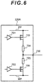
- Fig. 6 is a diagram for describing a second embodiment, and is a circuit diagram for showing a configuration example of an output circuit 320A configuring a part of the gate driver 320 of the power conversion device. It should be noted that circuit elements other than the output circuit 320A are not illustrated.
- complementary MOSFETs are employed for a P-MOSFET 703 and an N-MOSFET 706 as switching elements of the output circuit 320A.
- electric charges are discharged from a capacitor 1020 by turning on the N-MOSFET 706 and turning off the P-MOSFET 703 using an OFF command for setting the positive-side pre-buffer 701 high and the negative-side pre-buffer 702 high in the output circuit 320A in Fig. 6 .
- Fig. 7 is a block diagram of a power conversion device according to a third embodiment.
- the third embodiment clarifies that the gate wiring body 108 is a coaxial cable 200 of at least a part of gate wirings.
- the coaxial cable 200 is configured in such a manner that a plurality of conductors opposes each other in a planar manner with a minute interval therebetween. More specifically, two conductors are concentrically present, and can reduce the inductance.
- both ends of the coaxial cable 200 are of a so-called BNC type, the inductance at a connection part can be reduced by using a BCN-type connector of the gate driver 320.
- the coaxial cable 200 suppresses the inductance of the gate wiring by connecting an upper arm gate terminal 105 on the SiC module 300 side including an upper arm SiC 201 and a lower arm SiC 203 to an upper arm gate terminal 112 on the gate driver 320 side.
- an upper arm free-wheel diode 202 is connected to the upper arm SiC 201 in antiparallel and a lower arm free-wheel diode 204 is connected to the lower arm SiC 203 in antiparallel in the third embodiment.
- the above-described coaxial cable 200 may be provided at, at least a part of the gate wiring connecting the upper arm source auxiliary terminal 104 on the SiC module 300 side to the upper arm source auxiliary terminal 111 on the gate driver 320 side.
- the coaxial cable 200 may be provided at, at least, a part of the gate wiring connecting the lower arm gate terminal 107 on the SiC module 300 side to the lower arm gate terminal 114 on the gate driver 320 side, or may be provided at, at least, a part of the gate wiring connecting the lower arm source auxiliary terminal 109 on the SiC module 300 side to the lower arm source auxiliary terminal 113 on the gate driver 320 side.
- the inductance can be reduced, and thus the gate voltage can be prevented from fluctuating by the presence of such a coaxial cable 200 as compared to the linear gate wiring.
- Fig. 8 is a block diagram thereof.
- the IGBT module 300 is illustrated as a 1in1 type in which one element is accommodated in one package.
- the embodiment is different from the already-described embodiments in that the gate voltage can be more effectively prevented from fluctuating by the feedback capacitance 307 by providing the capacitor 1020 in addition to the gate wiring body bar 108.
- the signs in the IGBT module 300 in Fig. 8 are the same as those of the IGBT of the upper arm of Fig. 1 .
- the capacitor 1020 to suppress the fluctuation of the gate voltage is arranged between the gate driver 320 and the gate wiring bar 108, namely, on the gate driver 320 side relative to the switching module 300 or near the gate driver 320.
- One end of the capacitor 1020 is connected to a wiring 1120A connecting one of a pair of output terminals of the gate driver 320 to the conductor 108A, and the other end of the capacitor 1020 is connected to a wiring 1120B connecting the other output terminal of the gate driver 320 to the conductor 108B.
- the inductance of the gate wiring body 108 itself can be sufficiently reduced.
- the capacitor 1020 sufficiently absorbs a current flowing in from the feedback capacitance 307 by combining the capacitor 1020 for suppressing the fluctuation of the gate voltage to eliminate or remarkably reduce the current flowing into the input capacitance 308, so that the voltage of the gate terminal 303 is prevented from fluctuating.
- the capacitor 1020 for suppressing the fluctuation of the gate voltage is not directly connected to the switching module 300 but is connected between the gate wiring body 108 and the gate driver 320, a current flowing in from the feedback capacitance 105 can be sufficiently induced by the capacitor 1020 because the inductance of the gate wiring body 108 itself is sufficiently low.
- the optimum value of the capacitance of the capacitor 1020 may be selected in a range of half to twice the input capacitance of the IGBT 305.
- the input capacitance is about 100 nF
- the capacitance of the capacitor 1020 may be selected in a range of 50 nF to 200 nF.
- the capacitor 1020 is positioned on the gate driver 320 side apart from the switching module 300 through the gate wiring body 108, the capacitor 1020 is less affected by heat generation of the switching module 300, and the lifetime of the capacitor 1020 can be prevented from shortening.
- the function of the capacitor 1020 is not deteriorated.
- the fluctuation of the voltage of the gate terminal 303 of the IGBT 305 can be certainly suppressed over a long period, and the malfunction of the IGBT 305 can be prevented.
- the power conversion device performs power conversion by inputting a control signal from a pair of output terminals of the gate driver 320 to the switching module 300, the reliability of power conversion can be improved.
- the capacitor 1020 for suppressing the fluctuation of the gate voltage can be arranged apart from the switching module 300, it is not necessary to secure withstand voltage for the capacitor 1020. In addition, the cost of the capacitor 1020 can be suppressed, and the size thereof can be reduced.
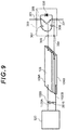
- Fig. 9 is a block diagram of a power conversion device according to a fifth embodiment.
- the fifth embodiment is different from the fourth embodiment in that a damping resistor 2010 connected in series to the capacitor 1020 between one wiring and the other wiring connecting the gate driver 320 to the gate wiring body 108 is provided.
- Equation (3) fc represents a resonance frequency
- Lg represents the inductance of a gate wiring unit 100
- Cg represents the capacitance of the capacitor 102 for suppressing the fluctuation of the gate voltage
- Cies represents an input capacitance
- the resonance can be suppressed by adding the damping resistor 2010 to the closed circuit, and the malfunction of the IGBT 305 caused by the resonance and the destruction of the IGBT 305 due to the overvoltage of the gate terminal 303 can be prevented.
- Fig. 10 is a block diagram of a power conversion device according to a sixth embodiment.
- the power conversion device according to the sixth embodiment includes a surge absorber 4010 that is arranged between one wiring and the other wiring connecting the gate driver 320 to the gate wiring body 108, and is connected in parallel with the capacitor 1020 for suppressing the fluctuation of the voltage of the gate terminal 303, so as to remove noise on the one wiring and the other wiring.
- the inductance of the wirings becomes small, and thus a surge voltage can be easily applied to the gate driver 320. Since a semiconductor element such as a comparator or an operational amplifier is present in the gate driver 320, the semiconductor element is destroyed by applying the surge voltage.
- the surge absorber 4010 is added near a pair of output terminals of the gate driver 320, the surge voltage is absorbed by the surge absorber 4010, and the gate driver 320 is protected from the surge voltage.
- Fig. 11 is a block diagram of a power conversion device according to a seventh embodiment.
- the gate wiring body bar 108 of Fig. 8 is changed to the coaxial cable 200, and the capacitor 1020 for suppressing the fluctuation of the gate voltage is added to the gate driver 320 side to suppress the fluctuation of the gate voltage.
- the switching element may be not only a wide band gap semiconductor using SiC, but also another wide band gap semiconductor using GaN or diamond.
- the switching element may be not only an IGBT or a power MOSFET, but also a J-FET or an SIT (Static Induction Transistor). Further, a so-called 2in1-type semiconductor obtained by accommodating two switching elements in one package and a 1in1-type semiconductor in which one switching element is mounted have been described in the above-described embodiments. However, a 6in1-type wide semiconductor in which six switching elements are mounted may be used.
- the present invention can be widely applied to a large-power power conversion device such as an inverter or converter used for a railroad vehicle driven by a motor, a steel rolling mill, a wind power generator, and the like.
- a large-power power conversion device such as an inverter or converter used for a railroad vehicle driven by a motor, a steel rolling mill, a wind power generator, and the like.
Landscapes
- Engineering & Computer Science (AREA)
- Power Engineering (AREA)
- Power Conversion In General (AREA)
- Inverter Devices (AREA)
- Electronic Switches (AREA)
Abstract
Description
- The present invention relates to a power conversion device and a power conversion method, and is particularly suitable for being applied to a large-power power conversion device used for a railroad vehicle driven by a motor, a steel rolling mill, a wind power generator, and the like.
- A power conversion device that converts large power between DC and AC for a railroad vehicle, a steel rolling mill, a wind power generator, and the like uses, as a switching element for power conversion, a power semiconductor element that can control a large current of several hundred amperes or larger under a high voltage exceeding 1 kV. For example, a power conversion device using an IGBT (Insulated Gate Bipolar Transistor) as a switching element has been known (Patent Literature 1).
- The IGBT is a composite bipolar element in which an input part has a MOSFET structure, an output part has a bipolar structure, and both of a low saturated voltage and a relatively-fast switching characteristic are realized. The IGBT includes two main terminals (a collector terminal and an emitter terminal) that energize a main power supply and a gate terminal as a control terminal that controls a current, and a gate drive circuit for controlling a gate voltage is connected to the gate terminal. When the gate drive circuit changes a gate voltage, a main current flowing between the collector terminal and the emitter terminal is controlled.
- On the other hand, in order to improve the efficiency of the power conversion device and to downsize the same, an element of a wide band gap semiconductor such as SiC (silicon carbide), GaN (gallium nitride), or diamond instead of silicon has been applied to the power conversion device (Nonpatent Literature 1).
- Since the dielectric breakdown field intensity of the wide band gap semiconductor is several times as large as silicon (about 10 times in the case of SiC and GaN and about 30 times in the case of diamond), the impurity concentration of a chip can be increased, and further the thickness of the chip can be configured thinner. Accordingly, conductive resistance at the time of current energization is reduced, and a conduction loss can be decreased. Thus, since the conductive resistance of a switching element is suppressed to be small, a power MOSFET having a faster switching characteristic and a unipolar structure instead of the IGBT having a bipolar structure can be used as the switching element. Further, while a silicon semiconductor can withstand up to about 200°C, the wide band gap semiconductor can withstand higher temperatures exceeding 200°C. Thus, the power converter can be downsized by simplifying a cooler of the power converter.
- [Patent Literature 1] Japanese Unexamined Patent Application Publication No.
2015-198545 - [Nonpatent Literature 1] "Gate-Driver with Full Protection for SiC-MOSFET Modules", VDE Conference Publication, Karsten Fink and Andreas Volke, Power Integrations GmbH, Germany, Winson Wei, Power Integrations, China, and Eugen Wiesner and Eckhard ThaI, Mitsubishi Electric Europe B.V., Germany, Date of Conference: 28-30 June 2016.
- A gate drive circuit is connected to a switching element through a wiring (gate wiring), and the wiring length is about 50 cm to 1 m. The wiring length is made long to prevent malfunction of the gate drive circuit due to electromagnetic noise at the time of switching performed by a power semiconductor element using a high voltage and a large current. Although it has been described that the cooler of the power conversion device can be downsized by applying the wide band gap semiconductor to the switching element of the power converter, the deterioration of the gate drive circuit can be suppressed by increasing the wiring length to avoid an influence of heat generation of the switching element on the gate drive circuit.
- In addition, when the switching element is turned off, or when the current of a free-wheel diode connected to the switching element in antiparallel is in an off state (hereinafter, also referred to as "reverse recovery"), a voltage between a collector and an emitter of the switching element is steeply changed, and thus a current flows to a gate from the collector through a feedback capacitance between the collector and the gate, leading to fluctuation of the gate voltage. As a result, malfunction of the switching element occurs. In order to avoid this, connection of a capacitor between gate and emitter terminals of the switching element has been also attempted.
- The fluctuation of the gate voltage due to the feedback capacitance is also increased in the wide band gap semiconductor. Even if the impurity concentration of a MOSFET using the wide band gap semiconductor is increased to reduce the resistance and the thickness thereof is reduced, the feedback capacitance is reversely increased.
- However, if an attempt to apply a capacitor to the switching element is made, there are problems that the capacitance of the capacitor is decreased due to heat generation at the time of switching when the capacitor is directly connected to the switching element, a connection part of the capacitor is disconnected, and the capacitor short-circuits.
- Accordingly, it is conceivable to connect the capacitor to the gate drive circuit side through the already-described long gate wiring. This configuration reduces an effect of suppressing the fluctuation of the gate voltage.
- In order to solve such problems, an object of the present invention is to propose a power conversion device and a power conversion method in which when a gate drive circuit is connected separately from a switching element and the temperature of the switching element becomes high due to a switching operation, malfunction of the switching element is prevented by suppressing fluctuation of a gate voltage to improve the reliability.
- In order to achieve the above-described object, the present invention provides a power conversion device that converts power between DC and AC, the device comprising: a switching module that includes a power semiconductor element as a switching element; a gate driver that outputs a drive signal for driving the switching element to a control terminal of the switching module; and a wiring body that connects the control terminal and an output terminal of the gate drive circuit using a plurality of conductors opposing each other in a planar manner with an interval therebetween. The present invention further relates to a power conversion method using the power conversion device.
- According to the present invention, it is possible to propose a power conversion device and a power conversion method in which when a gate drive circuit is connected separately from a switching element and the temperature of the switching element becomes high due to a switching operation, malfunction of the switching element is prevented by suppressing fluctuation of a gate voltage to improve the reliability.
-
-
Fig. 1 is a block diagram of a power conversion device according to a first embodiment. -
Fig. 2 is a perspective view of a gate wiring body of the power conversion device shown inFig. 1 when obliquely viewing the entirety of the gate wiring body. -
Fig. 3 is a circuit diagram for showing an electrical configuration example of the power conversion device shown inFig. 1 . -
Figs. 4 show an example of operation waveforms of the power conversion device shown inFig. 1 . -
Fig. 5 is a block diagram for showing a state in which a parasitic current flows. -
Fig. 6 is a block diagram of a power conversion device according to a second embodiment. -
Fig. 7 is a block diagram of a power conversion device according to a third embodiment. -
Fig. 8 is a block diagram of a power conversion device according to a fourth embodiment. -
Fig. 9 is a block diagram of a power conversion device according to a fifth embodiment. -
Fig. 10 is a block diagram of a power conversion device according to a sixth embodiment. -
Fig. 11 is a block diagram of a power conversion device according to a seventh embodiment. - Hereinafter, embodiments of the present invention will be described on the basis of the drawings.
Fig. 1 is a block diagram of a power conversion device according to a first embodiment, and is a block diagram of a switching system of a power conversion device in detail. Apower conversion device 1 includes aswitching module 300 having a switching element, a gate drive circuit (gate driver) 320, andgate wiring bodies 108 as wirings through which these are electrically connected to each other. - Hereinafter, the gate wiring bodies will be abbreviated as wirings or gate wirings in some cases. It should be noted that the
gate wiring bodies 108 are configured using a plurality of flat plate-like conductors as preferred embodiments as will be described later (Fig. 2 ), and thus will be also described asgate wiring bars 108. - In addition, the switching element may be an IGBT. Hereinafter, the
switching module 300 will be described as anIGBT module 300. It should be noted that the IBGT may be a silicon semiconductor or a wide band gap semiconductor. In addition, the switching element may be a power MOSFET (Metal-Oxide-Semiconductor Field-Effect Transistor) configured using a wide band gap semiconductor. - The explanation will be continued in accordance with
Fig. 1 . Thegate driver 320 includes an upper arm sourceauxiliary terminal 111, an upperarm gate terminal 112, a lower arm sourceauxiliary terminal 113, and a lowerarm gate terminal 114. - The
IGBT module 300 includes ACmain terminals 101, DC P-terminals 102, DC N-terminals 103, an upper arm sourceauxiliary terminal 104, an upper arm gate terminal 303 (corresponding to an upperarm gate terminal 105 to be described later), a lower arm source auxiliary terminal 106, and a lower arm gate terminal 313 (corresponding to a lowerarm gate terminal 107 to be described later). - The upper
arm gate terminal 112 is connected to the upperarm gate terminal 303 through thegate wiring bar 108, and the upper arm sourceauxiliary terminal 111 is provided near the upperarm gate terminal 112. The upper arm sourceauxiliary terminal 104 is provided near the upperarm gate terminal 303. - The lower
arm gate terminal 114 is connected to the lowerarm gate terminal 313 through thegate wiring bar 108, and the lower arm sourceauxiliary terminal 113 is provided near the lowerarm gate terminal 114. The lower arm source auxiliary terminal 106 is provided near the lowerarm gate terminal 313. - In the
IGBT module 300, two upper arm and lower arm DC P-terminals 102 and two upper arm and lower arm DC N-terminals 103 are provided, and two upper arm and lower arm ACmain terminals 101 are provided. - Next, the
gate wiring body 108 will be described in detail. Thegate wiring body 108 may be configured in such a mode that inductance between theIGBT module 300 and thegate driver 320 can be reduced in a range of one severalth to one several tenth as compared to wirings configured using conventional electric wires, and a plurality of conductors may oppose each other in a planar manner with a minute interval therebetween as a main mode. For example, at least, a pair of flat plate-like conductors that are parallel to each other may oppose each other. In other words, the "flat plate-like" may be changed to "rectangular", "planar", or "layered". - The
gate wiring body 108 can be manufactured in such a manner that a plurality of conductors is laminated so as to sandwich a thin film-like insulator therebetween to join the insulator and the conductors together in a laminated manner. As thegate wiring bodies 108, a plurality of conductors may oppose each other in a planar manner, and may be coaxially or concentrically combined with each other in addition to the flat plate-like conductors. Namely, an area where aconductor 108A opposes aconductor 108B is large, and an interval between theconductor 108A and theconductor 108B is set as small as possible to reduce inductance. The conductor may be made of material having conductivity such as copper or aluminum, or material such as iron or stainless material. The plane may be a flat plane or a curved plane. -
Fig. 2 is a perspective view of thegate wiring bar 108 shown inFig. 1 . Thegate wiring bar 108 is configured in such a manner that twoflat plates gate wiring bar 108 is set in accordance with configurations or arrangement of the twoflat plates flat plates gate wiring bar 108 is reduced. For the width W and the interval d of the twoflat plates
[Equation 1]
- In order to arrange the
flat plates gate wiring bar 108 is 5 mm and the interval between theflat plates flat plates flat plates - In the case where a power converter is an inverter applied to a train for a regular railroad line, the wiring length of the
gate wiring bar 108 is about 50 cm to 1 m. While the maximum inductance of wirings configured using a pair of electric wires is 1 µH, the inductance of thegate wiring bar 108 is reduced to 200 nH or smaller. - When the inductance in the case where the
gate driver 320 and theIGBT module 300 are connected to each other through an electric wire under the conditions where the interval between thegate driver 320 and theIGBT module 300 is 50 cm and the size of thegate wiring bar 108 is set as described above is compared to the inductance in the case where thegate driver 320 and theIGBT module 300 are connected to each other through thegate wiring bar 108, the former is about 350 nH whereas the latter is reduced to about 30 nH. -
Fig. 3 is a circuit diagram of theIGBT module 300 and thegate driver 320 as an electrical configuration example. TheIGBT module 300 is a so-called 2in1-type IGBT module. TwoIGBTs output terminal 325 connected to the above-described ACmain terminal 101. In theIGBT module 300, the lower arm has the same configuration as the upper arm, and thus the description of the upper arm is mainly substituted for that of the lower arm except for a case in which the lower arm needs to be particularly referred to. - In the
gate driver 320, the upper arm sourceauxiliary terminal 111, the upperarm gate terminal 112, the lower arm sourceauxiliary terminal 113, and the lowerarm gate terminal 114 described inFig. 1 are omitted. - An upper arm free-
wheel diode 306 is connected to theIGBT 305 in antiparallel. In the case where a current flows in the upper arm free-wheel diode 306 in the direction opposite to theIGBT 305, the current is recirculated. In the case where thepower semiconductor element 305 is a power MOSFET, a free-wheel diode 109 can be configured using, for example, a MOSFET-incorporated body diode. - On/off of the
IGBT 305 is controlled in accordance with a voltage applied to a gate terminal 303 (corresponding to an upper arm gate main terminal to be described later) and an emitterauxiliary terminal 304. When a positive voltage is applied to thegate terminal 303 in theIGBT 305, a current flows from anupper arm collector 330 towards anupper arm emitter 331. - The
gate driver 320 generates a voltage applied to thegate terminal 303 of theIGBT 305. Thegate driver 320 generates a gate voltage on the basis of a driving command from a gate command unit (gate command module) 322 that entirely controls the inverter system, and outputs the same to thegate terminal 303 of theIGBT 305. Thegate command unit 322 may be configured using software and/or hardware. - The
gate driver 320 and thegate command unit 322 are coupled to each other through aphoto coupler 324, and theIGBT 305 and the like to which a high voltage is applied are insulated from thegate command unit 322. A power supply for driving thegate driver 320 is supplied from agate power supply 321 through a gatepower supply transformer 323 that is an insulating transformer. - The
gate driver 320 and theIGBT module 300 are connected to each other through the twoflat plates gate wiring bar 108 in each case of the upper arm and the lower arm. While aparasitic capacitance 307 referred to as "feedback capacitance" is present between the upper arm collectormain terminal 301 connected to the DC P-terminal 102 and the upper arm gate main terminal 303 (corresponding to the gate terminal), and aparasitic capacitance 308 referred to as "input capacitance" is present between the upper arm gatemain terminal 303 and theupper arm emitter 331. - When the
IGBT 305 is switched, a parasitic current flows from the upper arm collectormain terminal 301 to the upper arm gatemain terminal 303 through theparasitic capacitance 307 referred to as "feedback capacitance" due to a steep change of a voltage applied between the upper arm collectormain terminal 301 and theupper arm emitter 331. Thus, there is a risk that the gate voltage of the upper arm gatemain terminal 303 fluctuates to cause malfunction. However, in the power conversion device according to the present invention, at least a part of wirings between thegate driver 320 and themodule 300 is changed to thegate wiring bar 108 so as not to cause such a phenomenon. - Each of
Fig. 4(A) to Fig. 4(C) shows an example of each waveform at the time of reverse recovery of the upper arm free-wheel diode 306 connected to theIGBT 305 in antiparallel. - In
Fig. 4(A) , the one-dot chain line shows an example of an anode current Ia of the upper arm free-wheel diode 306, and the two-dot chain line shows an example of a voltage Vac between the anode and the cathode of the upper arm free-wheel diode 306.Fig. 4(B) shows an example of a gate current Ig flowing in the upper arm gatemain terminal 303 of theIGBT 305, andFig. 4(C) shows an example of a gate voltage Vg in the upper arm gatemain terminal 303 of theIGBT 305. - As shown by the one-dot chain line in
Fig. 4(A) , the anode current Ia of the upper arm free-wheel diode 306 flowed in the forward direction until Time t1. However, a voltage Vac between the anode and the cathode fluctuates in the course of a turn of the flow thereafter as shown by the two-dot chain line inFig. 4(A) . As shown by the one-dot chain line inFig. 4(A) , a turn of the flow of the anode current Ia of the upper arm free-wheel diode 306 starts at Time t1. - As shown by the one-dot chain line in
Fig. 4(A) , when the anode current Ia becomes 0 at Time t2, a voltage is sharply applied to both ends (the upper arm collectormain terminal 301 and the upper arm emitter 331) of the upper arm free-wheel diode 306 as shown by the two-dot chain line inFig. 4(A) . Such a sharply-changed voltage is also applied to theIGBT 305 connected in antiparallel, and thus a voltage Vce between the upper arm collectormain terminal 301 and theupper arm emitter 331 in theIGBT 305 is changed in accordance with the voltage change rate dVce/dt. -
Fig. 5 shows an example of a state in which a parasitic current Igres flows between the upper arm collectormain terminal 301 and the upper arm gatemain terminal 303 in theIGBT 305. In general, theparasitic capacitance 307 referred to as "feedback capacitance" (the value of which is described as Cres) is present between the upper arm collectormain terminal 301 and the upper arm gatemain terminal 303 in theIGBT 305 as described above, and thus the parasitic current Igres shown in the following Equation (2) flows from the upper arm collectormain terminal 301 to the upper arm gatemain terminal 303 in accordance with the change of the voltage. - [Equation 2]

- The parasitic current Igres separately flows to the above-described input capacitance (the value of which is described as Cies) of the
IGBT 305 and thegate driver 320. If the impedance of the output circuit and the gate wiring of thegate driver 320 is small, the parasitic current Igres fully flows to thegate driver 320 and does not charge theparasitic capacitance 308 referred to as "input capacitance". Thus, the gate voltage of the gate wiring does not fluctuate. It should be noted that the gate wiring described herein corresponds to thegate wiring bar 108 in the case of the embodiment. - On the other hand, in the case where the impedance of the output circuit of the
gate driver 320 and theinductance 309 of the gate wiring (corresponding to thegate wiring bar 108 in the case of the embodiment) are large as described above, the parasitic current Igres flows to and charges theparasitic capacitance 308 referred to as "input capacitance". Thus, there is a risk that the gate voltage of the upper arm gatemain terminal 303 of theIGBT 305 is increased as shown inFig. 4(C) . - In the case where the parasitic current Igres is large, the
IGBT 305 is erroneously turned on if the gate voltage Vg of the upper arm gatemain terminal 303 exceeds a threshold value voltage Vt of theIGBT 305. Theinductance 309 of the gate wiring is dependent on the length of the gate wiring. As the length of the gate wiring becomes long, theinductance 309 is increased, and the possibility of erroneously turning on theIGBT 305 is enhanced. - As a countermeasure against such a phenomenon, at least a part of the gate wirings of the
IGBT 305 is configured using thegate wiring bar 108 including the pair offlat plates - In the
power conversion device 1 including thegate wiring bar 108 configured as described above, since the inductance of thegate wiring bar 108 is suppressed to be small by theseflat plates gate driver 320, and does not charge theparasitic capacitance 308 referred to as "input capacitance". In addition, the gate voltage of the gate wiring does not fluctuate. Thus, theIGBT 305 is prevented from being erroneously turned on. - If the
gate driver 320 is arranged apart from a position that is not affected by rise in temperature, the gate voltage of theIGBT 305 can be prevented from fluctuating by employing thegate wiring bar 108 having such a configuration to perform power conversion in the embodiment. Thus, even when thegate driver 320 is used at high temperatures where the performance of the wide band gap semiconductor is utilized, the reliability of thegate driver 320 is not deteriorated, and both of downsizing of the system and improvement in reliability can be realized along with high flexibility of arrangement. Moreover, since it is not necessary to arrange thegate driver 320 near a semiconductor element, the flexibility of arrangement can be enhanced, and the usability of thegate driver 320 can be improved by enhancing accessibility to thegate driver 320 at the time of maintenance. -
Fig. 6 is a diagram for describing a second embodiment, and is a circuit diagram for showing a configuration example of anoutput circuit 320A configuring a part of thegate driver 320 of the power conversion device. It should be noted that circuit elements other than theoutput circuit 320A are not illustrated. - The configurations and operations of the
output circuit 320A almost the same as those in the first embodiment will not be described, and different points between the both will be mainly described below. - In the second embodiment, as an example, complementary MOSFETs are employed for a P-
MOSFET 703 and an N-MOSFET 706 as switching elements of theoutput circuit 320A. - In the case where a predetermined driving command is input to each of a positive-
side pre-buffer 701 and a negative-side pre-buffer 702 when the IGBT and SiC element are turned on in theoutput circuit 320A, an output of the positive-side pre-buffer 701 becomes a low level, and the P-MOSFET 703 is turned on. On the other hand, the N-MOSFET 706 is turned off. Accordingly, a positive voltage is output from a positive power supply line PP to agate terminal 700 connected to the above-describedgate wiring bar 108, and thus theoutput circuit 320A turns on the IGBT and SiC element. - On the other hand, in the case where a predetermined driving command is input to each of the positive-
side pre-buffer 701 and the negative-side pre-buffer 702 when the IGBT and SiC element are turned off in theoutput circuit 320A, an output of the positive-side pre-buffer 701 is inverted to become a high level, and the P-MOSFET 703 is turned off. On the other hand, the N-MOSFET 706 is turned on. Accordingly, a negative voltage is output from a negative power supply line MP to thegate terminal 700 connected to the above-describedgate wiring bar 108, and thus theoutput circuit 320A turns off the IGBT and SiC element. - Even in the case where a current is about to flow due to the feedback capacitance of the SiC-MOSFET when the SiC-MOSFET is in an OFF state, an operation delay can be suppressed as compared to a bipolar transistor because instead of a bipolar transistor, a MOSFET that is a unipolar device is employed as a switching element of the
output circuit 320A in the embodiment. Therefore, according to the embodiment, the gate voltage of the SiC-MOSFET can be prevented from fluctuating as similar to the above-described first embodiment. - It should be noted that electric charges are discharged from a
capacitor 1020 by turning on the N-MOSFET 706 and turning off the P-MOSFET 703 using an OFF command for setting the positive-side pre-buffer 701 high and the negative-side pre-buffer 702 high in theoutput circuit 320A inFig. 6 . -
Fig. 7 is a block diagram of a power conversion device according to a third embodiment. The third embodiment clarifies that thegate wiring body 108 is acoaxial cable 200 of at least a part of gate wirings. As similar to the already-describedgate wiring bar 108, thecoaxial cable 200 is configured in such a manner that a plurality of conductors opposes each other in a planar manner with a minute interval therebetween. More specifically, two conductors are concentrically present, and can reduce the inductance. In general, since both ends of thecoaxial cable 200 are of a so-called BNC type, the inductance at a connection part can be reduced by using a BCN-type connector of thegate driver 320. - The
coaxial cable 200 suppresses the inductance of the gate wiring by connecting an upperarm gate terminal 105 on theSiC module 300 side including anupper arm SiC 201 and alower arm SiC 203 to an upperarm gate terminal 112 on thegate driver 320 side. - It should be noted that as similar to the already-described embodiments, an upper arm free-
wheel diode 202 is connected to theupper arm SiC 201 in antiparallel and a lower arm free-wheel diode 204 is connected to thelower arm SiC 203 in antiparallel in the third embodiment. - The above-described
coaxial cable 200 may be provided at, at least a part of the gate wiring connecting the upper arm sourceauxiliary terminal 104 on theSiC module 300 side to the upper arm sourceauxiliary terminal 111 on thegate driver 320 side. - On the other hand, also on the lower arm side as similar to the upper arm, the
coaxial cable 200 may be provided at, at least, a part of the gate wiring connecting the lowerarm gate terminal 107 on theSiC module 300 side to the lowerarm gate terminal 114 on thegate driver 320 side, or may be provided at, at least, a part of the gate wiring connecting the lower arm sourceauxiliary terminal 109 on theSiC module 300 side to the lower arm sourceauxiliary terminal 113 on thegate driver 320 side. - According to the third embodiment, as similar to the first and second embodiments, the inductance can be reduced, and thus the gate voltage can be prevented from fluctuating by the presence of such a
coaxial cable 200 as compared to the linear gate wiring. - Next, a power conversion device according to a fourth embodiment will be described.
Fig. 8 is a block diagram thereof. InFig. 8 , theIGBT module 300 is illustrated as a 1in1 type in which one element is accommodated in one package. The embodiment is different from the already-described embodiments in that the gate voltage can be more effectively prevented from fluctuating by thefeedback capacitance 307 by providing thecapacitor 1020 in addition to the gatewiring body bar 108. It should be noted that the signs in theIGBT module 300 inFig. 8 are the same as those of the IGBT of the upper arm ofFig. 1 . - The
capacitor 1020 to suppress the fluctuation of the gate voltage is arranged between thegate driver 320 and thegate wiring bar 108, namely, on thegate driver 320 side relative to theswitching module 300 or near thegate driver 320. One end of thecapacitor 1020 is connected to awiring 1120A connecting one of a pair of output terminals of thegate driver 320 to theconductor 108A, and the other end of thecapacitor 1020 is connected to awiring 1120B connecting the other output terminal of thegate driver 320 to theconductor 108B. - When the current of the free-
wheel diode 306 is off, namely, at the time of reverse recovery, a voltage between thecollector terminal 301 and theemitter terminal 331 is sharply increased, and a current flows from thecollector terminal 301 to thegate terminal 303 through thefeedback capacitance 307 along with a sharp increase in voltage. The current flows to thegate driver 320, and the potential rise of thegate terminal 303 can be suppressed. - When the inductance of the gate wiring is high, a current flows from the
feedback capacitance 307 to theinput capacitance 308, and thus the voltage of thegate terminal 303 is increased. When the voltage exceeds the threshold value voltage of theIGBT 305, theIGBT 305 is mistakenly turned on. - On the contrary, the inductance of the
gate wiring body 108 itself can be sufficiently reduced. In addition, thecapacitor 1020 sufficiently absorbs a current flowing in from thefeedback capacitance 307 by combining thecapacitor 1020 for suppressing the fluctuation of the gate voltage to eliminate or remarkably reduce the current flowing into theinput capacitance 308, so that the voltage of thegate terminal 303 is prevented from fluctuating. - Even if the
capacitor 1020 for suppressing the fluctuation of the gate voltage is not directly connected to theswitching module 300 but is connected between thegate wiring body 108 and thegate driver 320, a current flowing in from thefeedback capacitance 105 can be sufficiently induced by thecapacitor 1020 because the inductance of thegate wiring body 108 itself is sufficiently low. - The optimum value of the capacitance of the
capacitor 1020 may be selected in a range of half to twice the input capacitance of theIGBT 305. For example, in the case of an IGBT having a rated voltage of 3.3kV and a rated current of 1200 A, the input capacitance is about 100 nF, and the capacitance of thecapacitor 1020 may be selected in a range of 50 nF to 200 nF. - Since the
capacitor 1020 is positioned on thegate driver 320 side apart from theswitching module 300 through thegate wiring body 108, thecapacitor 1020 is less affected by heat generation of theswitching module 300, and the lifetime of thecapacitor 1020 can be prevented from shortening. - For example, even in the case where the
gate driver 320 has been used over a long period of about twenty years, the function of thecapacitor 1020 is not deteriorated. Thus, the fluctuation of the voltage of thegate terminal 303 of theIGBT 305 can be certainly suppressed over a long period, and the malfunction of theIGBT 305 can be prevented. As a result, even if the power conversion device performs power conversion by inputting a control signal from a pair of output terminals of thegate driver 320 to theswitching module 300, the reliability of power conversion can be improved. - Further, since the
capacitor 1020 for suppressing the fluctuation of the gate voltage can be arranged apart from theswitching module 300, it is not necessary to secure withstand voltage for thecapacitor 1020. In addition, the cost of thecapacitor 1020 can be suppressed, and the size thereof can be reduced. - Next,
Fig. 9 is a block diagram of a power conversion device according to a fifth embodiment. The fifth embodiment is different from the fourth embodiment in that a dampingresistor 2010 connected in series to thecapacitor 1020 between one wiring and the other wiring connecting thegate driver 320 to thegate wiring body 108 is provided. - When a frequency component of a current flowing into the gate through the
feedback capacitance 307 becomes the same as or near the resonance frequency of a closed circuit configured of thegate wiring body 108, thecapacitor 1020, and theinput capacitance 308, there is a possibility that resonance occurs in the closed circuit. The resonance condition is shown in Equation (3). - [Equation 3]

- In Equation (3), fc represents a resonance frequency, Lg represents the inductance of a gate wiring unit 100, Cg represents the capacitance of the
capacitor 102 for suppressing the fluctuation of the gate voltage, and Cies represents an input capacitance. - In the case where many components of the resonance frequency of Equation (3) are contained in a parasitic current flowing in from the
collector terminal 303 through thefeedback capacitance 307 at the time of reverse recovery of the free-wheel diode 306, there is a risk that resonance occurs and the gate voltage oscillates, resulting in malfunction of theIGBT 305, or an overvoltage occurs in thegate terminal 303 to destroy theIGBT 305. - The resonance can be suppressed by adding the damping
resistor 2010 to the closed circuit, and the malfunction of theIGBT 305 caused by the resonance and the destruction of theIGBT 305 due to the overvoltage of thegate terminal 303 can be prevented. - Next,
Fig. 10 is a block diagram of a power conversion device according to a sixth embodiment. The power conversion device according to the sixth embodiment includes asurge absorber 4010 that is arranged between one wiring and the other wiring connecting thegate driver 320 to thegate wiring body 108, and is connected in parallel with thecapacitor 1020 for suppressing the fluctuation of the voltage of thegate terminal 303, so as to remove noise on the one wiring and the other wiring. - If a part of gate wirings is replaced by the
gate wiring body 108, the inductance of the wirings becomes small, and thus a surge voltage can be easily applied to thegate driver 320. Since a semiconductor element such as a comparator or an operational amplifier is present in thegate driver 320, the semiconductor element is destroyed by applying the surge voltage. - Accordingly, if the
surge absorber 4010 is added near a pair of output terminals of thegate driver 320, the surge voltage is absorbed by thesurge absorber 4010, and thegate driver 320 is protected from the surge voltage. - Next,
Fig. 11 is a block diagram of a power conversion device according to a seventh embodiment. In the seventh embodiment, the gatewiring body bar 108 ofFig. 8 is changed to thecoaxial cable 200, and thecapacitor 1020 for suppressing the fluctuation of the gate voltage is added to thegate driver 320 side to suppress the fluctuation of the gate voltage. - The already-described embodiments are exemplifications for describing the present invention, and the present invention is not limited to these embodiments. For example, the switching element may be not only a wide band gap semiconductor using SiC, but also another wide band gap semiconductor using GaN or diamond.
- The switching element may be not only an IGBT or a power MOSFET, but also a J-FET or an SIT (Static Induction Transistor). Further, a so-called 2in1-type semiconductor obtained by accommodating two switching elements in one package and a 1in1-type semiconductor in which one switching element is mounted have been described in the above-described embodiments. However, a 6in1-type wide semiconductor in which six switching elements are mounted may be used.
- Even if all the gate wirings are not replaced by the
gate wiring bodies 108, a part of the gate wirings may be replaced by thegate wiring body 108 as long as the inductance can be reduced by a target amount. - The present invention can be widely applied to a large-power power conversion device such as an inverter or converter used for a railroad vehicle driven by a motor, a steel rolling mill, a wind power generator, and the like.
-
- 1 power conversion device
- 108 gate wiring bar
- 108A, 108B a pair of flat plates (conductors)
- 200 coaxial cable
- 300 IGBT module
- 320 gate driver (gate driving device)
- 320A output circuit
- 1020 capacitor (capacitor for suppressing fluctuation of gate voltage)
- 2010 damping resistor
- 4010 surge absorber
Claims (12)
- A power conversion device that converts power between DC and AC, the device comprising:a switching module that includes a power semiconductor element as a switching element;a gate driver that outputs a drive signal for driving the switching element to a control terminal of the switching module; anda wiring body that connects the control terminal and an output terminal of the gate drive circuit using a plurality of conductors opposing each other in a planar manner with an interval therebetween.
- The power conversion device according to claim 1,
wherein the wiring body includes a first conductor and a second conductor,
wherein the first conductor and the second conductor are configured using flat plates that are arranged in parallel with each other,
wherein the first conductor connects one terminal of the control terminals of the switching module to one terminal of the output terminals of the gate driver, and
wherein the second conductor connects the other terminal of the control terminals of the switching module to the other terminal of the output terminals of the gate driver. - The power conversion device according to claim 2,
wherein when each width of the first conductor and the second conductor is W and an interval between the first conductor and the second conductor is d, W×5≥d is satisfied. - The power conversion device according to claim 1,
wherein an output circuit of the gate driver includes a MOSFET. - The power conversion device according to claim 1,
wherein the wiring body includes a first conductor and a second conductor, and
wherein a capacitor is connected between a first wiring connecting the gate driver to the first conductor and a second wiring connecting the gate driver to the second conductor. - The power conversion device according to claim 5,
wherein a resistor is connected in series to the capacitor between the first wiring and the second wiring. - The power conversion device according to claim 5,
wherein a surge absorber is connected in parallel with the capacitor between the first wiring and the second wiring. - The power conversion device according to claim 1,
wherein the switching element is an insulated gate bipolar transistor or a metal-oxide-semiconductor field-effect transistor. - The power conversion device according to claim 1,
wherein the wiring body is a coaxial cable in which the first conductor and the second conductor are coaxially arranged. - The power conversion device according to claim 1,
wherein the gate driver is arranged apart from the switching module in a range of 50 cm to 1 m. - A power conversion method using a power conversion device that converts power between DC and AC and comprises a switching module that includes a power semiconductor element as a switching element, a gate driver that outputs a drive signal for driving the switching element to a control terminal of the switching module, and a wiring body that connects the control terminal and an output terminal of the gate drive circuit,
wherein the switching module accumulates a current based on a feedback capacitance between a main terminal of the switching module and the control terminal into a capacitor through the wiring body, so that fluctuation of a voltage of the control terminal is suppressed. - The power conversion method according to claim 11,
wherein the wiring body connects the control terminal and an output terminal of the gate drive circuit using a plurality of conductors opposing each other in a planar manner with an interval therebetween.
Applications Claiming Priority (3)
| Application Number | Priority Date | Filing Date | Title |
|---|---|---|---|
| JP2017165563 | 2017-08-30 | ||
| JP2017192238 | 2017-09-29 | ||
| PCT/JP2018/031769 WO2019044832A1 (en) | 2017-08-30 | 2018-08-28 | Power conversion device and power conversion method |
Publications (3)
| Publication Number | Publication Date |
|---|---|
| EP3678287A1 true EP3678287A1 (en) | 2020-07-08 |
| EP3678287A4 EP3678287A4 (en) | 2021-05-05 |
| EP3678287B1 EP3678287B1 (en) | 2023-11-22 |
Family
ID=65527479
Family Applications (1)
| Application Number | Title | Priority Date | Filing Date |
|---|---|---|---|
| EP18851051.5A Active EP3678287B1 (en) | 2017-08-30 | 2018-08-28 | Power conversion device and power conversion method |
Country Status (4)
| Country | Link |
|---|---|
| EP (1) | EP3678287B1 (en) |
| JP (1) | JP6795702B2 (en) |
| CN (1) | CN111052577B (en) |
| WO (1) | WO2019044832A1 (en) |
Families Citing this family (5)
| Publication number | Priority date | Publication date | Assignee | Title |
|---|---|---|---|---|
| JP7351209B2 (en) * | 2019-12-17 | 2023-09-27 | 富士電機株式会社 | semiconductor equipment |
| WO2021225111A1 (en) * | 2020-05-07 | 2021-11-11 | 株式会社豊田自動織機 | Power conversion device |
| JP7488373B2 (en) | 2021-01-15 | 2024-05-21 | 株式会社日立製作所 | Wiring structure of control line, railway power converter having the same, and control line laying method |
| WO2022185703A1 (en) * | 2021-03-03 | 2022-09-09 | 株式会社日立製作所 | Control line wiring structure, railway power converter having same, and control line laying method |
| JP2024055057A (en) * | 2022-10-06 | 2024-04-18 | 株式会社日立製作所 | Electrical Equipment |
Family Cites Families (13)
| Publication number | Priority date | Publication date | Assignee | Title |
|---|---|---|---|---|
| JP2845524B2 (en) * | 1989-11-20 | 1999-01-13 | 電気興業株式会社 | Gate drive circuit for static induction transistors |
| JP2997025B2 (en) * | 1990-09-04 | 2000-01-11 | 株式会社日立製作所 | Power converter |
| DE19702949A1 (en) * | 1997-01-28 | 1998-07-30 | Stribel Gmbh | Control unit |
| JPH10257754A (en) * | 1997-03-14 | 1998-09-25 | Toshiba Corp | Gate drive circuit for current-controlled switching element |
| JP3376245B2 (en) * | 1997-05-22 | 2003-02-10 | 三菱電機株式会社 | Semiconductor switching device, semiconductor stack device and power conversion device using the same |
| JP4803928B2 (en) * | 2001-09-13 | 2011-10-26 | 東芝エレベータ株式会社 | Power converter |
| JP3791393B2 (en) * | 2001-10-23 | 2006-06-28 | 富士電機デバイステクノロジー株式会社 | Inverter circuit |
| JP5492518B2 (en) * | 2009-10-02 | 2014-05-14 | 株式会社日立製作所 | Semiconductor drive circuit and semiconductor device using the same |
| DE102009046258B3 (en) * | 2009-10-30 | 2011-07-07 | Infineon Technologies AG, 85579 | Power semiconductor module and method for operating a power semiconductor module |
| JP5569141B2 (en) * | 2010-05-18 | 2014-08-13 | 富士電機株式会社 | Power conversion device, discrete type control type semiconductor element and control type semiconductor element module |
| US8487407B2 (en) * | 2011-10-13 | 2013-07-16 | Infineon Technologies Ag | Low impedance gate control method and apparatus |
| JP6425380B2 (en) * | 2013-12-26 | 2018-11-21 | ローム株式会社 | Power circuit and power module |
| JP6230946B2 (en) * | 2014-04-03 | 2017-11-15 | 株式会社日立製作所 | Power conversion device and railway vehicle equipped with the same |
-
2018
- 2018-08-28 EP EP18851051.5A patent/EP3678287B1/en active Active
- 2018-08-28 JP JP2019539531A patent/JP6795702B2/en active Active
- 2018-08-28 WO PCT/JP2018/031769 patent/WO2019044832A1/en not_active Ceased
- 2018-08-28 CN CN201880054985.2A patent/CN111052577B/en active Active
Also Published As
| Publication number | Publication date |
|---|---|
| JPWO2019044832A1 (en) | 2020-07-02 |
| JP6795702B2 (en) | 2020-12-02 |
| EP3678287A4 (en) | 2021-05-05 |
| CN111052577A (en) | 2020-04-21 |
| EP3678287B1 (en) | 2023-11-22 |
| CN111052577B (en) | 2023-07-25 |
| WO2019044832A1 (en) | 2019-03-07 |
Similar Documents
| Publication | Publication Date | Title |
|---|---|---|
| EP3678287B1 (en) | Power conversion device and power conversion method | |
| US10896896B2 (en) | Semiconductor device comprising PN junction diode and schottky barrier diode | |
| US8791662B2 (en) | Power semiconductor module, electric-power conversion apparatus, and railway vehicle | |
| US20100321847A1 (en) | Semiconductor power conversion apparatus | |
| US9276401B2 (en) | Solid state circuit-breaker switch devices | |
| JP5977836B2 (en) | Method, power unit and power system having gate voltage limiting circuit | |
| US10554150B2 (en) | Three-level inverter | |
| US8570780B2 (en) | Semiconductor device | |
| US20180226966A1 (en) | Circuit arrangement for an electronic device | |
| GB2533212A (en) | Power conversion device and railway vehicle including the same | |
| EP2320545B1 (en) | Converter with voltage limiting component | |
| EP2768128A1 (en) | Three-level brake chopper and three-level converter | |
| KR20150002479A (en) | Power semiconductor circuit | |
| US11146168B2 (en) | Snubber circuit and power conversion apparatus | |
| WO2024220370A1 (en) | Integrated bidirectional four quadrant switches with drivers and input/output circuits | |
| US11679680B2 (en) | Power module for operating an electric vehicle drive with an intermediate circuit capacitor | |
| US11005359B2 (en) | Electric power converter with snubber circuit | |
| US11398418B2 (en) | Semiconductor module | |
| CN117375458A (en) | solid state motor starter | |
| CN117595200A (en) | Overvoltage protection circuit |
Legal Events
| Date | Code | Title | Description |
|---|---|---|---|
| STAA | Information on the status of an ep patent application or granted ep patent |
Free format text: STATUS: THE INTERNATIONAL PUBLICATION HAS BEEN MADE |
|
| PUAI | Public reference made under article 153(3) epc to a published international application that has entered the european phase |
Free format text: ORIGINAL CODE: 0009012 |
|
| STAA | Information on the status of an ep patent application or granted ep patent |
Free format text: STATUS: REQUEST FOR EXAMINATION WAS MADE |
|
| 17P | Request for examination filed |
Effective date: 20200218 |
|
| AK | Designated contracting states |
Kind code of ref document: A1 Designated state(s): AL AT BE BG CH CY CZ DE DK EE ES FI FR GB GR HR HU IE IS IT LI LT LU LV MC MK MT NL NO PL PT RO RS SE SI SK SM TR |
|
| AX | Request for extension of the european patent |
Extension state: BA ME |
|
| DAV | Request for validation of the european patent (deleted) | ||
| DAX | Request for extension of the european patent (deleted) | ||
| A4 | Supplementary search report drawn up and despatched |
Effective date: 20210409 |
|
| RIC1 | Information provided on ipc code assigned before grant |
Ipc: H02M 1/08 20060101AFI20210401BHEP Ipc: H03K 17/687 20060101ALI20210401BHEP Ipc: H03K 17/16 20060101ALI20210401BHEP Ipc: H02M 7/00 20060101ALI20210401BHEP Ipc: H03K 17/0812 20060101ALI20210401BHEP |
|
| GRAP | Despatch of communication of intention to grant a patent |
Free format text: ORIGINAL CODE: EPIDOSNIGR1 |
|
| STAA | Information on the status of an ep patent application or granted ep patent |
Free format text: STATUS: GRANT OF PATENT IS INTENDED |
|
| RIC1 | Information provided on ipc code assigned before grant |
Ipc: H03K 17/0812 20060101ALI20230524BHEP Ipc: H02M 7/00 20060101ALI20230524BHEP Ipc: H03K 17/16 20060101ALI20230524BHEP Ipc: H03K 17/687 20060101ALI20230524BHEP Ipc: H02M 1/08 20060101AFI20230524BHEP |
|
| INTG | Intention to grant announced |
Effective date: 20230613 |
|
| GRAS | Grant fee paid |
Free format text: ORIGINAL CODE: EPIDOSNIGR3 |
|
| GRAA | (expected) grant |
Free format text: ORIGINAL CODE: 0009210 |
|
| STAA | Information on the status of an ep patent application or granted ep patent |
Free format text: STATUS: THE PATENT HAS BEEN GRANTED |
|
| AK | Designated contracting states |
Kind code of ref document: B1 Designated state(s): AL AT BE BG CH CY CZ DE DK EE ES FI FR GB GR HR HU IE IS IT LI LT LU LV MC MK MT NL NO PL PT RO RS SE SI SK SM TR |
|
| REG | Reference to a national code |
Ref country code: GB Ref legal event code: FG4D |
|
| REG | Reference to a national code |
Ref country code: CH Ref legal event code: EP Ref country code: DE Ref legal event code: R096 Ref document number: 602018061584 Country of ref document: DE |
|
| REG | Reference to a national code |
Ref country code: IE Ref legal event code: FG4D |
|
| REG | Reference to a national code |
Ref country code: LT Ref legal event code: MG9D |
|
| REG | Reference to a national code |
Ref country code: NL Ref legal event code: MP Effective date: 20231122 |
|
| PG25 | Lapsed in a contracting state [announced via postgrant information from national office to epo] |
Ref country code: GR Free format text: LAPSE BECAUSE OF FAILURE TO SUBMIT A TRANSLATION OF THE DESCRIPTION OR TO PAY THE FEE WITHIN THE PRESCRIBED TIME-LIMIT Effective date: 20240223 |
|
| PG25 | Lapsed in a contracting state [announced via postgrant information from national office to epo] |
Ref country code: IS Free format text: LAPSE BECAUSE OF FAILURE TO SUBMIT A TRANSLATION OF THE DESCRIPTION OR TO PAY THE FEE WITHIN THE PRESCRIBED TIME-LIMIT Effective date: 20240322 |
|
| PG25 | Lapsed in a contracting state [announced via postgrant information from national office to epo] |
Ref country code: LT Free format text: LAPSE BECAUSE OF FAILURE TO SUBMIT A TRANSLATION OF THE DESCRIPTION OR TO PAY THE FEE WITHIN THE PRESCRIBED TIME-LIMIT Effective date: 20231122 |
|
| REG | Reference to a national code |
Ref country code: AT Ref legal event code: MK05 Ref document number: 1634774 Country of ref document: AT Kind code of ref document: T Effective date: 20231122 |
|
| PG25 | Lapsed in a contracting state [announced via postgrant information from national office to epo] |
Ref country code: NL Free format text: LAPSE BECAUSE OF FAILURE TO SUBMIT A TRANSLATION OF THE DESCRIPTION OR TO PAY THE FEE WITHIN THE PRESCRIBED TIME-LIMIT Effective date: 20231122 |
|
| PG25 | Lapsed in a contracting state [announced via postgrant information from national office to epo] |
Ref country code: AT Free format text: LAPSE BECAUSE OF FAILURE TO SUBMIT A TRANSLATION OF THE DESCRIPTION OR TO PAY THE FEE WITHIN THE PRESCRIBED TIME-LIMIT Effective date: 20231122 |
|
| PG25 | Lapsed in a contracting state [announced via postgrant information from national office to epo] |
Ref country code: ES Free format text: LAPSE BECAUSE OF FAILURE TO SUBMIT A TRANSLATION OF THE DESCRIPTION OR TO PAY THE FEE WITHIN THE PRESCRIBED TIME-LIMIT Effective date: 20231122 |
|
| PG25 | Lapsed in a contracting state [announced via postgrant information from national office to epo] |
Ref country code: NL Free format text: LAPSE BECAUSE OF FAILURE TO SUBMIT A TRANSLATION OF THE DESCRIPTION OR TO PAY THE FEE WITHIN THE PRESCRIBED TIME-LIMIT Effective date: 20231122 Ref country code: LT Free format text: LAPSE BECAUSE OF FAILURE TO SUBMIT A TRANSLATION OF THE DESCRIPTION OR TO PAY THE FEE WITHIN THE PRESCRIBED TIME-LIMIT Effective date: 20231122 Ref country code: IS Free format text: LAPSE BECAUSE OF FAILURE TO SUBMIT A TRANSLATION OF THE DESCRIPTION OR TO PAY THE FEE WITHIN THE PRESCRIBED TIME-LIMIT Effective date: 20240322 Ref country code: GR Free format text: LAPSE BECAUSE OF FAILURE TO SUBMIT A TRANSLATION OF THE DESCRIPTION OR TO PAY THE FEE WITHIN THE PRESCRIBED TIME-LIMIT Effective date: 20240223 Ref country code: ES Free format text: LAPSE BECAUSE OF FAILURE TO SUBMIT A TRANSLATION OF THE DESCRIPTION OR TO PAY THE FEE WITHIN THE PRESCRIBED TIME-LIMIT Effective date: 20231122 Ref country code: BG Free format text: LAPSE BECAUSE OF FAILURE TO SUBMIT A TRANSLATION OF THE DESCRIPTION OR TO PAY THE FEE WITHIN THE PRESCRIBED TIME-LIMIT Effective date: 20240222 Ref country code: AT Free format text: LAPSE BECAUSE OF FAILURE TO SUBMIT A TRANSLATION OF THE DESCRIPTION OR TO PAY THE FEE WITHIN THE PRESCRIBED TIME-LIMIT Effective date: 20231122 Ref country code: PT Free format text: LAPSE BECAUSE OF FAILURE TO SUBMIT A TRANSLATION OF THE DESCRIPTION OR TO PAY THE FEE WITHIN THE PRESCRIBED TIME-LIMIT Effective date: 20240322 |
|
| PG25 | Lapsed in a contracting state [announced via postgrant information from national office to epo] |
Ref country code: SE Free format text: LAPSE BECAUSE OF FAILURE TO SUBMIT A TRANSLATION OF THE DESCRIPTION OR TO PAY THE FEE WITHIN THE PRESCRIBED TIME-LIMIT Effective date: 20231122 Ref country code: RS Free format text: LAPSE BECAUSE OF FAILURE TO SUBMIT A TRANSLATION OF THE DESCRIPTION OR TO PAY THE FEE WITHIN THE PRESCRIBED TIME-LIMIT Effective date: 20231122 Ref country code: PL Free format text: LAPSE BECAUSE OF FAILURE TO SUBMIT A TRANSLATION OF THE DESCRIPTION OR TO PAY THE FEE WITHIN THE PRESCRIBED TIME-LIMIT Effective date: 20231122 Ref country code: NO Free format text: LAPSE BECAUSE OF FAILURE TO SUBMIT A TRANSLATION OF THE DESCRIPTION OR TO PAY THE FEE WITHIN THE PRESCRIBED TIME-LIMIT Effective date: 20240222 Ref country code: LV Free format text: LAPSE BECAUSE OF FAILURE TO SUBMIT A TRANSLATION OF THE DESCRIPTION OR TO PAY THE FEE WITHIN THE PRESCRIBED TIME-LIMIT Effective date: 20231122 Ref country code: HR Free format text: LAPSE BECAUSE OF FAILURE TO SUBMIT A TRANSLATION OF THE DESCRIPTION OR TO PAY THE FEE WITHIN THE PRESCRIBED TIME-LIMIT Effective date: 20231122 |
|
| PG25 | Lapsed in a contracting state [announced via postgrant information from national office to epo] |
Ref country code: DK Free format text: LAPSE BECAUSE OF FAILURE TO SUBMIT A TRANSLATION OF THE DESCRIPTION OR TO PAY THE FEE WITHIN THE PRESCRIBED TIME-LIMIT Effective date: 20231122 |
|
| PG25 | Lapsed in a contracting state [announced via postgrant information from national office to epo] |
Ref country code: CZ Free format text: LAPSE BECAUSE OF FAILURE TO SUBMIT A TRANSLATION OF THE DESCRIPTION OR TO PAY THE FEE WITHIN THE PRESCRIBED TIME-LIMIT Effective date: 20231122 |
|
| PG25 | Lapsed in a contracting state [announced via postgrant information from national office to epo] |
Ref country code: SK Free format text: LAPSE BECAUSE OF FAILURE TO SUBMIT A TRANSLATION OF THE DESCRIPTION OR TO PAY THE FEE WITHIN THE PRESCRIBED TIME-LIMIT Effective date: 20231122 |
|
| PG25 | Lapsed in a contracting state [announced via postgrant information from national office to epo] |
Ref country code: SM Free format text: LAPSE BECAUSE OF FAILURE TO SUBMIT A TRANSLATION OF THE DESCRIPTION OR TO PAY THE FEE WITHIN THE PRESCRIBED TIME-LIMIT Effective date: 20231122 Ref country code: SK Free format text: LAPSE BECAUSE OF FAILURE TO SUBMIT A TRANSLATION OF THE DESCRIPTION OR TO PAY THE FEE WITHIN THE PRESCRIBED TIME-LIMIT Effective date: 20231122 Ref country code: RO Free format text: LAPSE BECAUSE OF FAILURE TO SUBMIT A TRANSLATION OF THE DESCRIPTION OR TO PAY THE FEE WITHIN THE PRESCRIBED TIME-LIMIT Effective date: 20231122 Ref country code: EE Free format text: LAPSE BECAUSE OF FAILURE TO SUBMIT A TRANSLATION OF THE DESCRIPTION OR TO PAY THE FEE WITHIN THE PRESCRIBED TIME-LIMIT Effective date: 20231122 Ref country code: DK Free format text: LAPSE BECAUSE OF FAILURE TO SUBMIT A TRANSLATION OF THE DESCRIPTION OR TO PAY THE FEE WITHIN THE PRESCRIBED TIME-LIMIT Effective date: 20231122 Ref country code: CZ Free format text: LAPSE BECAUSE OF FAILURE TO SUBMIT A TRANSLATION OF THE DESCRIPTION OR TO PAY THE FEE WITHIN THE PRESCRIBED TIME-LIMIT Effective date: 20231122 |
|
| REG | Reference to a national code |
Ref country code: DE Ref legal event code: R097 Ref document number: 602018061584 Country of ref document: DE |
|
| PLBE | No opposition filed within time limit |
Free format text: ORIGINAL CODE: 0009261 |
|
| STAA | Information on the status of an ep patent application or granted ep patent |
Free format text: STATUS: NO OPPOSITION FILED WITHIN TIME LIMIT |
|
| PG25 | Lapsed in a contracting state [announced via postgrant information from national office to epo] |
Ref country code: SI Free format text: LAPSE BECAUSE OF FAILURE TO SUBMIT A TRANSLATION OF THE DESCRIPTION OR TO PAY THE FEE WITHIN THE PRESCRIBED TIME-LIMIT Effective date: 20231122 |
|
| 26N | No opposition filed |
Effective date: 20240823 |
|
| PG25 | Lapsed in a contracting state [announced via postgrant information from national office to epo] |
Ref country code: SI Free format text: LAPSE BECAUSE OF FAILURE TO SUBMIT A TRANSLATION OF THE DESCRIPTION OR TO PAY THE FEE WITHIN THE PRESCRIBED TIME-LIMIT Effective date: 20231122 |
|
| REG | Reference to a national code |
Ref country code: DE Ref legal event code: R119 Ref document number: 602018061584 Country of ref document: DE |
|
| REG | Reference to a national code |
Ref country code: CH Ref legal event code: PL |
|
| PG25 | Lapsed in a contracting state [announced via postgrant information from national office to epo] |
Ref country code: LU Free format text: LAPSE BECAUSE OF NON-PAYMENT OF DUE FEES Effective date: 20240828 |
|
| PG25 | Lapsed in a contracting state [announced via postgrant information from national office to epo] |
Ref country code: MC Free format text: LAPSE BECAUSE OF FAILURE TO SUBMIT A TRANSLATION OF THE DESCRIPTION OR TO PAY THE FEE WITHIN THE PRESCRIBED TIME-LIMIT Effective date: 20231122 Ref country code: CH Free format text: LAPSE BECAUSE OF NON-PAYMENT OF DUE FEES Effective date: 20240831 |
|
| REG | Reference to a national code |
Ref country code: BE Ref legal event code: MM Effective date: 20240831 |
|
| PG25 | Lapsed in a contracting state [announced via postgrant information from national office to epo] |
Ref country code: DE Free format text: LAPSE BECAUSE OF NON-PAYMENT OF DUE FEES Effective date: 20250301 |
|
| PG25 | Lapsed in a contracting state [announced via postgrant information from national office to epo] |
Ref country code: BE Free format text: LAPSE BECAUSE OF NON-PAYMENT OF DUE FEES Effective date: 20240831 |
|
| PG25 | Lapsed in a contracting state [announced via postgrant information from national office to epo] |
Ref country code: FR Free format text: LAPSE BECAUSE OF NON-PAYMENT OF DUE FEES Effective date: 20240831 |
|
| PG25 | Lapsed in a contracting state [announced via postgrant information from national office to epo] |
Ref country code: IE Free format text: LAPSE BECAUSE OF NON-PAYMENT OF DUE FEES Effective date: 20240828 |
|
| PG25 | Lapsed in a contracting state [announced via postgrant information from national office to epo] |
Ref country code: FI Free format text: LAPSE BECAUSE OF FAILURE TO SUBMIT A TRANSLATION OF THE DESCRIPTION OR TO PAY THE FEE WITHIN THE PRESCRIBED TIME-LIMIT Effective date: 20231122 |
|
| PGFP | Annual fee paid to national office [announced via postgrant information from national office to epo] |
Ref country code: IT Payment date: 20250821 Year of fee payment: 8 |
|
| PGFP | Annual fee paid to national office [announced via postgrant information from national office to epo] |
Ref country code: GB Payment date: 20250721 Year of fee payment: 8 |
|
| PG25 | Lapsed in a contracting state [announced via postgrant information from national office to epo] |
Ref country code: CY Free format text: LAPSE BECAUSE OF FAILURE TO SUBMIT A TRANSLATION OF THE DESCRIPTION OR TO PAY THE FEE WITHIN THE PRESCRIBED TIME-LIMIT; INVALID AB INITIO Effective date: 20180828 |
|
| PG25 | Lapsed in a contracting state [announced via postgrant information from national office to epo] |
Ref country code: HU Free format text: LAPSE BECAUSE OF FAILURE TO SUBMIT A TRANSLATION OF THE DESCRIPTION OR TO PAY THE FEE WITHIN THE PRESCRIBED TIME-LIMIT; INVALID AB INITIO Effective date: 20180828 |