EP3678196A1 - Substrate for mounting electronic components, electronic device, and electronic module - Google Patents
Substrate for mounting electronic components, electronic device, and electronic module Download PDFInfo
- Publication number
- EP3678196A1 EP3678196A1 EP18851332.9A EP18851332A EP3678196A1 EP 3678196 A1 EP3678196 A1 EP 3678196A1 EP 18851332 A EP18851332 A EP 18851332A EP 3678196 A1 EP3678196 A1 EP 3678196A1
- Authority
- EP
- European Patent Office
- Prior art keywords
- conductor
- electronic component
- insulating substrate
- component mounting
- substrate
- Prior art date
- Legal status (The legal status is an assumption and is not a legal conclusion. Google has not performed a legal analysis and makes no representation as to the accuracy of the status listed.)
- Granted
Links
Images





Classifications
-
- H—ELECTRICITY
- H10—SEMICONDUCTOR DEVICES; ELECTRIC SOLID-STATE DEVICES NOT OTHERWISE PROVIDED FOR
- H10W—GENERIC PACKAGES, INTERCONNECTIONS, CONNECTORS OR OTHER CONSTRUCTIONAL DETAILS OF DEVICES COVERED BY CLASS H10
- H10W70/00—Package substrates; Interposers; Redistribution layers [RDL]
- H10W70/60—Insulating or insulated package substrates; Interposers; Redistribution layers
- H10W70/62—Insulating or insulated package substrates; Interposers; Redistribution layers characterised by their interconnections
- H10W70/63—Vias, e.g. via plugs
- H10W70/635—Through-vias
-
- H—ELECTRICITY
- H10—SEMICONDUCTOR DEVICES; ELECTRIC SOLID-STATE DEVICES NOT OTHERWISE PROVIDED FOR
- H10W—GENERIC PACKAGES, INTERCONNECTIONS, CONNECTORS OR OTHER CONSTRUCTIONAL DETAILS OF DEVICES COVERED BY CLASS H10
- H10W70/00—Package substrates; Interposers; Redistribution layers [RDL]
- H10W70/60—Insulating or insulated package substrates; Interposers; Redistribution layers
- H10W70/62—Insulating or insulated package substrates; Interposers; Redistribution layers characterised by their interconnections
- H10W70/65—Shapes or dispositions of interconnections
-
- H—ELECTRICITY
- H05—ELECTRIC TECHNIQUES NOT OTHERWISE PROVIDED FOR
- H05K—PRINTED CIRCUITS; CASINGS OR CONSTRUCTIONAL DETAILS OF ELECTRIC APPARATUS; MANUFACTURE OF ASSEMBLAGES OF ELECTRICAL COMPONENTS
- H05K3/00—Apparatus or processes for manufacturing printed circuits
- H05K3/46—Manufacturing multilayer circuits
-
- H—ELECTRICITY
- H10—SEMICONDUCTOR DEVICES; ELECTRIC SOLID-STATE DEVICES NOT OTHERWISE PROVIDED FOR
- H10H—INORGANIC LIGHT-EMITTING SEMICONDUCTOR DEVICES HAVING POTENTIAL BARRIERS
- H10H20/00—Individual inorganic light-emitting semiconductor devices having potential barriers, e.g. light-emitting diodes [LED]
- H10H20/80—Constructional details
- H10H20/85—Packages
- H10H20/857—Interconnections, e.g. lead-frames, bond wires or solder balls
-
- H—ELECTRICITY
- H10—SEMICONDUCTOR DEVICES; ELECTRIC SOLID-STATE DEVICES NOT OTHERWISE PROVIDED FOR
- H10W—GENERIC PACKAGES, INTERCONNECTIONS, CONNECTORS OR OTHER CONSTRUCTIONAL DETAILS OF DEVICES COVERED BY CLASS H10
- H10W70/00—Package substrates; Interposers; Redistribution layers [RDL]
- H10W70/60—Insulating or insulated package substrates; Interposers; Redistribution layers
- H10W70/67—Insulating or insulated package substrates; Interposers; Redistribution layers characterised by their insulating layers or insulating parts
- H10W70/68—Shapes or dispositions thereof
- H10W70/685—Shapes or dispositions thereof comprising multiple insulating layers
-
- H—ELECTRICITY
- H10—SEMICONDUCTOR DEVICES; ELECTRIC SOLID-STATE DEVICES NOT OTHERWISE PROVIDED FOR
- H10H—INORGANIC LIGHT-EMITTING SEMICONDUCTOR DEVICES HAVING POTENTIAL BARRIERS
- H10H20/00—Individual inorganic light-emitting semiconductor devices having potential barriers, e.g. light-emitting diodes [LED]
- H10H20/80—Constructional details
- H10H20/85—Packages
- H10H20/8506—Containers
-
- H—ELECTRICITY
- H10—SEMICONDUCTOR DEVICES; ELECTRIC SOLID-STATE DEVICES NOT OTHERWISE PROVIDED FOR
- H10W—GENERIC PACKAGES, INTERCONNECTIONS, CONNECTORS OR OTHER CONSTRUCTIONAL DETAILS OF DEVICES COVERED BY CLASS H10
- H10W70/00—Package substrates; Interposers; Redistribution layers [RDL]
- H10W70/01—Manufacture or treatment
- H10W70/05—Manufacture or treatment of insulating or insulated package substrates, or of interposers, or of redistribution layers
- H10W70/098—Applying pastes or inks, e.g. screen printing
-
- H—ELECTRICITY
- H10—SEMICONDUCTOR DEVICES; ELECTRIC SOLID-STATE DEVICES NOT OTHERWISE PROVIDED FOR
- H10W—GENERIC PACKAGES, INTERCONNECTIONS, CONNECTORS OR OTHER CONSTRUCTIONAL DETAILS OF DEVICES COVERED BY CLASS H10
- H10W90/00—Package configurations
- H10W90/701—Package configurations characterised by the relative positions of pads or connectors relative to package parts
- H10W90/721—Package configurations characterised by the relative positions of pads or connectors relative to package parts of bump connectors
- H10W90/724—Package configurations characterised by the relative positions of pads or connectors relative to package parts of bump connectors between a chip and a stacked insulating package substrate, interposer or RDL
-
- H—ELECTRICITY
- H10—SEMICONDUCTOR DEVICES; ELECTRIC SOLID-STATE DEVICES NOT OTHERWISE PROVIDED FOR
- H10W—GENERIC PACKAGES, INTERCONNECTIONS, CONNECTORS OR OTHER CONSTRUCTIONAL DETAILS OF DEVICES COVERED BY CLASS H10
- H10W90/00—Package configurations
- H10W90/701—Package configurations characterised by the relative positions of pads or connectors relative to package parts
- H10W90/751—Package configurations characterised by the relative positions of pads or connectors relative to package parts of bond wires
- H10W90/754—Package configurations characterised by the relative positions of pads or connectors relative to package parts of bond wires between a chip and a stacked insulating package substrate, interposer or RDL
Definitions
- the present invention relates to an electronic component mounting substrate, an electronic device, and an electronic module.
- an electronic component mounting substrate and an electronic device are known, for mounting electronic components on a main surface of an insulating substrate made of ceramics.
- the insulating substrate has a recess portion on an upper surface for housing and mounting each of the electronic components, and includes a conductor layer on a bottom surface of the recess portion, a conductor layer on a lower surface to be connected to a module substrate, and a via conductor between the conductor layers (referred to, for example, Japanese Unexamined Patent Application Publication No. 2015-159245 ).
- An electronic component mounting substrate of the present disclosure includes an insulating substrate for mounting an electronic component; a via conductor disposed in the insulating substrate in a thickness direction of the insulating substrate; and a via pad conductor disposed in the insulating substrate, connected to the via conductor, having a thickness gradually increasing from an outer edge portion toward an inside portion, and including a protruding portion protruding from the via conductor in a width direction of the via conductor.
- An electronic device of the present disclosure includes the electronic component mounting substrate according to the configuration described above; and an electronic component mounted on the recess portion.
- An electronic module of the present disclosure includes a module substrate including a connection pad; and the electronic device connected to the connection pad via solder.
- an electronic device includes an electronic component mounting substrate 1 and an electronic component 2 mounted on a recess portion 14 of the electronic component mounting substrate 1.
- the electronic device is connected to, for example, a module substrate 4 constituting an electronic module by using solder 5.
- the electronic component mounting substrate 1 in the first embodiment includes an insulating substrate 11 for mounting the electronic component 2, a via conductor 12 positioned in the insulating substrate 11 in a thickness direction, and a via pad conductor 13 positioned in the insulating substrate 11, connected to the via conductor 12, having a thickness that gradually increases from an outer edge portion toward an inside portion, and including a protruding portion 13a that protrudes from the via conductor 12 in a width direction of the via conductor 12.
- the insulating substrate 11 has a recess portion 14 for mounting the electronic component 2 on one main surface, and conductor layers 15 are positioned on a surface and an inside of the recess portion 14. In Figs.
- an upward direction refers to a positive direction of a virtual z axis.
- a distinction between top and bottom in the following description is for convenience, and there is no intention to restrict the top and bottom if the electronic component mounting substrate 1 or the like is actually used.
- the conductor layers 15 are indicated by shading, if viewed in a plan view, and a portion overlapping a side surface of the via conductor 12 is indicated by a dotted line.
- the via conductor pad 13 and the conductor layer 15 are indicated by shading, if viewed in a plan view, and a portion overlapping the side surface of the via conductor 12 and a portion overlapping an inner wall of the recess portion 14 are indicated by dotted lines.
- the insulating substrate 11 has one main surface (upper surface in Figs. 1 to 4 ), the other main surface (lower surface in Figs. 1 to 4 ) opposite to the main surface, and a side surface.
- the insulating substrate 11 is configured of a plurality of insulating layers 11a, is open to the main surface, and has the recess portion 14 for mounting the electronic component 2.
- the insulating substrate 11 has a shape of a rectangular plate, if viewed in a plan view, that is, viewed in a direction perpendicular to the main surface.
- the insulating substrate 11 functions as a support for supporting the electronic component 2, and the electronic component 2 is bonded and fixed to a mounting portion on a bottom surface of the recess portion 14, via a connection member 3 such as solder bump, gold bump, conductive resin (anisotropic conductive resin, or the like), or resin.
- a connection member 3 such as solder bump, gold bump, conductive resin (anisotropic conductive resin, or the like), or resin.
- the insulating substrate 11 for example, ceramics such as an aluminum oxide sintered body (alumina ceramics), an aluminum nitride sintered body, a silicon nitride sintered body, a mullite sintered body, or a glass ceramic sintered body can be used. If the insulating substrate 11 is, for example, the aluminum oxide sintered body, an appropriate organic binder and a solvent are added and mixed to a raw material powder such as aluminum oxide (Al 2 O 3 ), silicon oxide (SiO 2 ), magnesium oxide (MgO), or calcium oxide (CaO), and the like to product a slurry.
- a raw material powder such as aluminum oxide (Al 2 O 3 ), silicon oxide (SiO 2 ), magnesium oxide (MgO), or calcium oxide (CaO), and the like to product a slurry.
- a ceramic green sheet is produced by forming the slurry in a sheet form by using a well-known doctor blade method, a calendar roll method, or the like of the related art. Next, an appropriate punching process is performed on the ceramic green sheet, and a plurality of ceramic green sheets is laminated to form a green body, and the green body is fired at a high temperature (approximately 1,600°C), whereby the insulating substrate 11 is produced.
- the recess portion 14 is positioned on the main surface of the insulating substrate 11.
- the recess portion 14 is for mounting the electronic component 2 on the bottom surface.
- the recess portion 14 has a rectangular shape with a corner having a round shape, if viewed in a plan view, and is positioned at a center portion of the insulating substrate 11.
- the insulating substrate 11 is formed of four insulating layers 11a, and the recess portion 14 is positioned in first and second insulating layers 11a on one main surface side.
- insulating layers 11a are formed between the bottom surface of the recess portion 14 and the other main surface of the insulating substrate 11.
- the example illustrated in Fig. 2(a) is a top view of an inside of the bottom surface on the recess portion 14, that is, a third insulating layer 11a on the one main surface side, if viewed in a plan view.
- the example illustrated in Fig. 2(b) is a top view of an inside between the bottom surface of the recess portion 14 of the recess portion 14 and the other main surface of the insulating substrate 11, that is, of a fourth insulating layer 11a on the one main surface side, if viewed in a plan view.
- the recess portion 14 can be formed, for example, by forming a through-hole to be the recess portion 14 in each ceramic green sheet by a laser process, a punching with a mold in a portion of the ceramic green sheets for the insulating substrate 11, and laminating the ceramic green sheets on other ceramic green sheets in which no through-hole is formed.
- the via conductors 12, the via pad conductors 13, and the conductor layers 15 are positioned on the surface and the inside of the insulating substrate 11.
- the via conductors 12, the via pad conductors 13, and the conductor layers 15 are for electrically connecting the electronic component 2 and the module substrate 4.
- the conductor layers 15 are positioned on the bottom surface of the recess portion 14 and the other main surface of the insulating substrate 11.
- the via conductor 12 is positioned in the insulating substrate 11 in the thickness direction (z direction in Figs. 1 to 3 ), and an end portion of the via conductor 12 is connected to the conductor layer 15.
- the via pad conductor 13 is positioned in the insulating substrate 11, and is positioned between the via conductor 12 on a bottom surface side of the recess portion 14 and the via conductor 12 on the other main surface side of the insulating substrate 11.
- the upper surface and the lower surface of the via pad conductor are respectively connected to the via conductors 12.
- the via conductor 12 is positioned so as to overlap the recess portion 14, if viewed in a plan view.
- the via conductors 12 are positioned in at least two insulating layers 11a respectively in the thickness direction of the insulating substrate 11 between the bottom surface of the recess portion 14 and the other main surface of the insulating substrate 11.
- the via pad conductor 13 gradually increases in thickness from the outer edge portion toward the center portion and has the protruding portion 13a extending from the via conductor 12 in the width direction of the via conductor 12.
- the protruding portion 13a of the via pad conductor 13 extends from each of the via conductor 12 connected to the upper surface of the via pad conductor 13 and the via conductor 12 connected to the lower surface thereof in the width direction of the via conductor 12.
- the width direction of the via conductor 12 is any direction of a width (diameter) of the via conductor 12 in a planar direction, if viewed in a plan view.
- the protruding portion 13a extending from the via conductor 12 in the width direction of the via conductor 12 means that the protruding portion 13a of the via pad conductor 13 extends to an outside beyond the side surface of the via conductor 12, if viewed in a plan view.
- the via pad conductor 13 has the protruding portion 13a extending from the via conductor 12 over an entire periphery of the side surface of the via conductor 12.
- the via conductor 12, the via pad conductor 13, and the conductor layer 15 are, for example, formed by metallization of metal powder mainly composed of tungsten (W), molybdenum (Mo), manganese (Mn), silver (Ag), copper (Cu), or the like.
- the insulating substrate 11 is made of the aluminum oxide sintered body
- a metallized paste obtained by adding and mixing an appropriate organic binder and a solvent or the like to a high-melting-point metal powder such as W, Mo, or Mn is preliminarily printed and applied to the ceramic green sheet for the insulating substrate 11 in a predetermined pattern by a screen printing method, and is fired at the same time as the ceramic green sheet for the insulating substrate 11 to be deposited and formed at a predetermined position of the insulating substrate 11.
- the via pad conductor 13 and the conductor layer 15 are formed by, for example, printing and applying a metallized paste for the via pad conductor 13 and the conductor layer 15 on the ceramic green sheet for the insulating substrate 11 by printing means such as a screen printing method, and firing the metallized paste together with the ceramic green sheet for the insulating substrate 11.
- the via conductor 12 is formed, for example, by forming a through-hole for the via conductor 12 in the ceramic green sheet for the insulating substrate 11 by a processing method such as a punching with a mold, or a laser process, filling the through-hole with the metallized paste for the via conductor 12 by the printing means, and firing the metallized paste together with the ceramic green sheet for the insulating substrate 11.
- the metallized paste is produced by appropriately adjusting the viscosity by adding an appropriate solvent and binder to the metal powder described above and kneading.
- glass powder or ceramic powder may be included.
- the via pad conductor 13 gradually increases in thickness from the outer edge portion toward the inside portion.
- the via pad conductor 13 can be formed, for example, by making the thickness of the inside greater than the thickness of the outer edge portion side, if the metallized paste for the via pad conductor 13 is printed on the surface of the ceramic green sheet, on the metallized paste for the via conductor 12, with which the through-hole for the via conductor 12 formed in the ceramic green sheet for the insulating substrate 11 is filled.
- a metal plating layer is deposited on the surface of the conductor layer 15 exposed from the insulating substrate 11 by an electroplating method or an electroless plating method.
- the metal plating layer is made of metal having good corrosion resistance and good connection member connectivity, such as nickel, copper, gold, or silver.
- a nickel plating layer having a thickness of approximately 0.5 to 5 ⁇ m and a gold plating layer having a thickness of approximately 0.1 to 3 ⁇ m are deposited sequentially. Therefore, the corrosion of the conductor layer 15 can be effectively suppressed, bonding between the conductor layer 15 and the connection member 3 such as a bonding wire, and bonding between the conductor layer 15 and a connection pad 41 for connection positioned on the module substrate 4 can be strengthened.
- the metal plating layer is not limited to the nickel plating layer/gold plating layer, and may be other metal plating layers including a nickel plating layer/palladium plating layer/gold plating layer, and the like.
- the electronic device can be produced by mounting the electronic component 2 on the bottom surface of the recess portion 14 of the electronic component mounting substrate 1.
- the electronic component 2 for mounting on the electronic component mounting substrate 1 is a semiconductor element such as an IC chip or an LSI chip, a light emitting element, a piezoelectric element such as a crystal oscillator or a piezoelectric vibrator, or various sensors.
- the electronic component 2 is a wire-bonding-type semiconductor element
- the semiconductor element is fixed to the bottom surface of the recess portion 14 with a bonding member such as a low-melting-point brazing material or a conductive resin, and then the electrode of the semiconductor element and the conductor layer 15 are electrically connected via the connection member 3 such as a bonding wire, and thereby the semiconductor element is mounted on the electronic component mounting substrate 1.
- the electronic component 2 is electrically connected to the conductor layer 15.
- the electrode of the semiconductor element and the conductor layer 15 are electrically and mechanically connected to each other via the connection member 3 such as a solder bump, a gold bump, or a conductive resin (anisotropic conductive resin or the like), and thereby the semiconductor element is mounted on the electronic component mounting substrate 1.
- a plurality of electronic components 2 may be mounted on the bottom surface of the recess portion 14 of the electronic component mounting substrate 1, or a small electronic component such as a resistor element or a capacitor element may be mounted, as necessary.
- the electronic component 2 is sealed by using a sealing material made of resin, glass, or the like, or a lid made of resin, glass, ceramics, metal, or the like, as necessary.
- the conductor layer 15 of the electronic device of the present embodiment is connected to the connection pad 41 of the module substrate 4 via the solder 5 to form the electronic module.
- the conductor layer 15 positioned on the other main surface of the electronic component mounting substrate 1 is connected to the connection pad 41 of the module substrate 4.
- the electronic component mounting substrate 1 of the present embodiment includes the insulating substrate 11 for mounting the electronic component 2, the via conductor 12 positioned in the insulating substrate 11 in the thickness direction, and the via pad conductor 13 positioned in the insulating substrate 11, connected to the via conductor 12, having a thickness that gradually increases from the outer edge portion toward the inside portion, and including the protruding portion 13a protruding from the via conductor 12 in the width direction of the via conductor 12.
- the stress is applied to the electronic device including the electronic component mounting substrate 1 in a planar direction and the stress is applied to the via conductor 12 by an external force during handling, the stress is dispersed by the via pad conductor 13 of which the thickness gradually increases from the outer edge portion toward the inside portion, generation of a gap between the insulating substrate 11 and the via conductor 12 is suppressed, and reduction of airtightness between the recess portion 14 and the lower surface of the insulating substrate 11 can be suppressed.
- the end portion of the protruding portion 13a is pointed, for example, even if the stress is applied to the electronic device including the electronic component mounting substrate 1 in the planar direction, and the stress is applied to the via conductor 12 by an external force during handling, the stress is further dispersed by the via pad conductor 13 having a larger inclined surface from the outer edge portion toward the inside portion, and generation of the gap between the insulating substrate 11 and the via conductor 12 is further suppressed, and reduction of the airtightness between the recess portion 14 and the lower surface of the insulating substrate 11 can be suppressed. Sharpness indicates that the thickness of the via pad conductor 13 is reduced, if viewed in a longitudinal sectional view.
- the protruding portion 13a of the via pad conductor 13 protrudes from the via conductors 12 over an entire periphery of the side surface of the via conductors 12 in the width direction, which are connected to the upper surface and the lower surface, the stress is dispersed by the via pad conductor 13 over the entire periphery of the side surface of the via conductors 12 in the width direction, generation of the gap between the insulating substrate 11 and the via conductors 12 is suppressed, and reduction of the airtightness between the recess portion 14 and the lower surface of the insulating substrate 11 can be suppressed.
- the thickness of the center portion of the via pad conductor 13 is larger than the thickness of the outer edge portion thereof, if viewed in a longitudinal sectional view, for example, even if the stress in the planar direction is applied to the electronic device including the electronic component mounting substrate 1 and the stress is applied to the via conductor 12 by the external force during handling, the stress is dispersed by the via pad conductor 13 of which the thickness of the center portion is larger than the thickness of the outer edge portion.
- the stress is effectively dispersed at a portion that is in contact from the center portion to the outer edge portion of the via pad conductor 13, generation of the gap between the insulating substrate 11 and the via conductor 12 is suppressed, and reduction of the airtightness between the recess portion 14 and the lower surface of the insulating substrate 11 can be suppressed.
- thicknesses H11 and H12 of the respective insulating layers 11a where the via conductors 12 are positioned across the via pad conductor 13 may be within ⁇ 10% of one insulating layer 11a (0.9H12 ⁇ H11 ⁇ 1.1H12). In this case, the stress applied to each via conductor 12 is easily dispersed evenly between the bottom surface side of the recess portion 14 and the lower surface side of the insulating substrate 11.
- a maximum thickness H2 of the via pad conductor 13 is equal to or greater than a difference between the thicknesses H11 and H12 (H2 ⁇
- the stress is applied to the electronic device including the electronic component mounting substrate 1 in the planar direction and the stress is applied to the via conductor 12 by the external force during handling and a gap may easily be generated between the insulating substrate 11 and the via conductor 12, the airtightness is easily maintained at a portion where the one end portion of the via conductor 12 in the width direction is in contact with the protruding portion 13a, the protruding portion 13a, and a portion where the protruding portion 13a is in contact with the insulating substrate 11.
- reduction of the airtightness between the recess portion 14 and the lower surface of the insulating substrate 11 can be suppressed.
- both end portions of the via conductor 12 in the width direction are in contact with the protruding portion 13a, if for example, the stress is applied to the electronic device including the electronic component mounting substrate 1 in the planar direction and the stress is applied to the via conductor 12 by the external force during handling and a gap may easily be generated between the insulating substrate 11 and the both end portions of the via conductor 12 in the width direction, the airtightness is further easily maintained at a portion where the both end portions of the via conductor 12 in the width direction are in contact with the protruding portion 13a, the protruding portion 13a, and a portion where the protruding portion 13a is in contact with the insulating substrate 11.
- the outer edge of the entire periphery of the via conductor 12 in the width direction may be connected to the protruding portion 13a.
- an inclination of a contact surface between the via conductor 12 and the via pad conductor 13 is larger than an inclination of a contact surface between the insulating layer 11a and the via pad conductor 13, for example, even if the stress is applied to the electronic device including the electronic component mounting substrate in the planar direction and the stress is applied to the via conductor by the external force during handling, the stress is effectively dispersed by the via pad conductor in which the inclination of the contact surface between the via conductor 12 and the via pad conductor 13 is large.
- the inclination of the contact surface between the via conductor 12 and the via pad conductor 13 may be larger than the inclination of the contact surface between the insulating layer 11a and the via pad conductor 13, and the protruding portion 13a may be connected, at the outer edge of the entire periphery of the via conductor 12 in the width direction.
- such via conductors 12 and via pad conductors 13 can be formed as follows. If the through-hole for the via conductor 12 in the ceramic green sheet for the insulating substrate 11 is filled with the metallized paste for the via conductor 12, an opening of the through-hole for the via conductor 12 is filled with the metallized paste for the via conductor 12 so that a sectional view has a recessed-curved surface shape (shape that is recessed from the outer edge portion of the opening toward the center portion of the opening), and the through-hole for the via conductor 12 is filled with the metallized paste for the via pad conductor 13 on the metallized paste for the via conductor 12, whereby the via conductors 12 and the via pad conductors 13 are formed on the surface of the ceramic green sheet by printing.
- the content ratio of ceramic contained in the via pad conductor 13 may be higher than the content ratio of ceramic contained in the via conductor 12.
- the content ratio of ceramic contained in the via pad conductor 13 may be as high as approximately 1.2 to 2 times the content ratio of ceramic contained in the via conductor 12. Therefore, a resistance difference between the via pad conductor 13 and the via conductor 12 having a smaller area, if viewed in a plan view, than that of the via pad conductor 13 is reduced, the contact between the via conductor 12 and the via pad conductor 13 is good, and a shift between the via conductor 12 and the via pad conductor 13 is suppressed. Therefore, reduction of the airtightness between the recess portion 14 and the lower surface of the insulating substrate 11 can be suppressed.
- the electronic device includes the electronic component mounting substrate 1 having the configuration described above, and the electronic component 2 mounted on the electronic component mounting substrate 1, and thereby an electronic device having good long-term reliability can be obtained.
- the electronic module of the present embodiment includes the module substrate 4 having the connection pad 41 and the electronic device having the configuration described above connected to the connection pad 41 via the solder 5, and thereby having good long-term reliability.
- the electronic component mounting substrate 1 in the present embodiment can be suitably used in a thin and high-power electronic device.
- the electronic component mounting substrate 1 can be suitably used if the diameter of the via conductor 12 is smaller than a height of the via conductor 12.
- a light emitting element such as an LED
- the airtightness of the recess portion 14 is good and the electronic component mounting substrate 1 can be suitably used as the electronic component mounting substrate 1 for a thin and high-luminance light emitting device.
- the electronic device according to the second embodiment is different from the electronic device according to the embodiment described above in that a plurality of via conductors 12 is connected to an upper surface and a lower surface of one via pad conductor 13, respectively.
- a plurality of via conductors 12 is connected to an upper surface and a lower surface of one via pad conductor 13, respectively.
- two via conductors 12 are connected to the upper surface of one via pad conductor 13, and two via conductors 12 are connected to the lower surface of one via pad conductor 13.
- the conductor layers 15 are indicated by shading, if viewed in a plan view, and a portion overlapping a side surface of the via conductor 12 is indicated by a dotted line.
- the via conductor pads 13 and the conductor layers 15 are indicated by shading, and a portion overlapping the side surface of the via conductor 12 and a portion overlapping an inner wall of the recess portion 14 are indicated by dotted lines.
- the electronic component mounting substrate 1 of the second embodiment similarly to the electronic component mounting substrate 1 of the first embodiment, for example, even if the stress in the planar direction is applied to an electronic device including the electronic component mounting substrate 1 and the stress is applied to the individual via conductors 12 by an external force during handling, the stress is dispersed by the via pad conductor of which the thickness gradually increases from the outer edge portion toward the inside portion, generation of a gap between the insulating substrate 11 and the individual via conductors 12 is suppressed, and reduction of the airtightness between the recess portion 14 and the lower surface of the insulating substrate 11 can be suppressed.
- a thickness of the via pad conductor 13 between the plurality of via conductors 12, if viewed in a longitudinal sectional view is smaller than a thickness of the via pad conductor 13 in a region overlapping the via conductors 12, if viewed in a plan view.
- the via pad conductor 13 connected to the plurality of via conductors 12 includes protruding portion 13a protruding from the plurality of via conductors 12 in the width direction of the via conductor 12.
- the protruding portion 13a of the via pad conductor 13 extends from each of the plurality of via conductors 12 connected to the upper surface of the via pad conductor 13 and the plurality of via conductors 12 connected to the lower surface thereof in the width direction of the via conductor 12.
- the protruding portion 13a of the via pad conductor 13 protrudes from each via conductor 12 over an entire periphery of the side surface in the width direction of the plurality of the via conductors 12 connected to the upper surface and the lower surface, the stress is dispersed by the via pad conductor 13 over the entire periphery of the side surface of the via conductors 12 in the width direction, generation of the gap between the insulating substrate 11 and the via conductor 12 is suppressed, and reduction of the airtightness between the recess portion 14 and the lower surface of the insulating substrate 11 can be suppressed.
- the thickness of the via pad conductor 13 between the plurality of via conductors 12 if viewed in a plan view may be larger than the thickness of the via pad conductor 13 in a region overlapping the via conductors 12, if viewed in a sectional view.
- the electronic component mounting substrate 1 of the second embodiment can be produced by using the same producing method as that of the electronic component mounting substrate 1 of the embodiment described above.
- the electronic component mounting substrate 1 of the second embodiment can be suitably used in a thin and high-power electronic device.
- the electronic component mounting substrate 1 can be suitably used if the diameter of the via conductor 12 is smaller than a height of the via conductor 12.
- a light emitting element such as an LED
- the airtightness of the recess portion 14 is good and the electronic component mounting substrate 1 can be suitably used as the electronic component mounting substrate 1 for a thin and high-luminance light emitting device.
- the electronic device according to the third embodiment is different from the electronic device according to the embodiments described above in that the number of via conductors 12 connected to the upper surface of one via pad conductor 13 is different from the number of via conductors 12 connected to the lower surface of one via pad 13.
- two via conductors 12 are connected to the upper surface of one via pad conductor 13, and one via conductor 12 is connected to the lower surface of the one via pad conductor 13.
- the electronic component mounting substrate 1 of the third embodiment similarly to the electronic component mounting substrate 1 of the first embodiment, for example, even if the stress in the planar direction is applied to an electronic device including the electronic component mounting substrate 1 and the stress is applied to the via conductor 12 by an external force during handling, the stress is dispersed by the via pad conductor 13 of which the thickness gradually increases from the outer edge portion toward the inside portion, generation of a gap between the insulating substrate 11 and the via conductors 12 is suppressed.
- the via conductor 12 on the bottom surface side of the recess portion 14 and the via conductor 12 on the lower surface side of the insulating substrate 11 are positioned not to overlap each other across the via pad conductor 13, if viewed in a plan view, so that the stress applied to the via pad conductor 13 is dispersed in the planar direction, and reduction of the airtightness between the recess portion 14 and the lower surface of the insulating substrate 11 can be effectively suppressed.
- each via conductor 12 connected to the lower surface of one via pad 13 is positioned between the via conductors 12 connected to the upper surface of one via pad conductor 13, if viewed in a longitudinal sectional view.
- the via conductors 12 connected to the upper surface of one via pad conductor 13 and each via conductor 12 connected to the lower surface of one via pad 13 are positioned so as not to overlap each other, if viewed in a plan view.
- the via pad conductor 13 connected to the plurality of via conductors 12 includes the protruding portions 13a protruding from the plurality of via conductors 12 in the width direction of the via conductors 12.
- the protruding portion 13a of the via pad conductor 13 extends from each of the plurality of via conductors 12 connected to the upper surface of the via pad conductor 13 and the via conductor 12 connected to the lower surface thereof in the width direction of the via conductor 12.
- the protruding portion 13a of the via pad conductor 13 protrudes from each via conductor 12 over an entire periphery of the side surface in the width direction of the plurality of the via conductors 12 connected to the upper surface and the lower surface, the stress is dispersed by the via pad conductor 13 over the entire periphery of the side surface of the via conductors 12 in the width direction, generation of the gap between the insulating substrate 11 and the via conductor 12 is suppressed, and reduction of the airtightness between the recess portion 14 and the lower surface of the insulating substrate 11 can be suppressed.
- the electronic component mounting substrate 1 of the third embodiment can be produced by using the same producing method as that of the electronic component mounting substrate 1 of the embodiments described above.
- the electronic component mounting substrate 1 of the third embodiment can be suitably used in a thin and high-power electronic device.
- the electronic component mounting substrate 1 can be suitably used if the diameter of the via conductor 12 is smaller than a height of the via conductor 12.
- a light emitting element such as an LED
- the airtightness of the recess portion 14 is good and the electronic component mounting substrate 1 can be suitably used as the electronic component mounting substrate 1 for a thin and high-luminance light emitting device.
- the insulating substrate 11 may have a rectangular shape including a notch portion or a chamfered portion on a side surface or at a corner, if viewed in a plan view.
- a notch may be positioned from the side surface of the insulating substrate 11 to the other main surface, and a conductor connected to the conductor layer 15 and positioned on an inner surface of the notch, that is, a castellation conductor may be included.
- the inner wall surface of the recess portion 14 is positioned perpendicular to the bottom surface of the recess portion 14, if viewed in a sectional view.
- the inner wall surface of the recess portion 14 may be an inclined surface so that, in the inner wall surface of the recess portion 14, an opening side is wider than a bottom surface side of the recess portion 14.
- a metal layer may be positioned on the inner wall surface of the recess portion 14.
- the electronic component mounting substrate 1 can be suitably used as the electronic component mounting substrate 1 for a light emitting device having good light emission luminance.
- the inclination of the contact surface between the via conductor 12 and the via pad conductor 13 may be larger than the inclination of the contact surface between the insulating layer 11a and the via pad conductor 13.
- the recess portion 14 has a substantially rectangular shape, if viewed in a plan view, but may have another shape such as a circular shape, if viewed in a plan view.
- the insulating substrate 11 is configured of four insulating layers 11a.
- the insulating substrate 11 may be configured of two, three, or five or more insulating layers 11a.
- the recess portion 14 may be a recess portion 14 of which an inner wall surface is stepped, if viewed in a longitudinal sectional view.
- the electronic component mounting substrates 1 of the first to third embodiments have the recess portion 14 positioned on one main surface, but may not have a recess portion, that is, the electronic component mounting substrate 1 having a flat insulating substrate 11 may be provided.
- the airtightness between the one main surface of the insulating substrate 11 and the other main surface of the insulating substrate 11 can be improved.
- the electronic component mounting substrate 1 may be produced in a form of a multi-piece substrate.
Landscapes
- Engineering & Computer Science (AREA)
- Manufacturing & Machinery (AREA)
- Microelectronics & Electronic Packaging (AREA)
- Production Of Multi-Layered Print Wiring Board (AREA)
- Physics & Mathematics (AREA)
- Geometry (AREA)
- Led Device Packages (AREA)
Abstract
Description
- The present invention relates to an electronic component mounting substrate, an electronic device, and an electronic module.
- In the related art, an electronic component mounting substrate and an electronic device are known, for mounting electronic components on a main surface of an insulating substrate made of ceramics.
- In such an electronic component mounting substrate, the insulating substrate has a recess portion on an upper surface for housing and mounting each of the electronic components, and includes a conductor layer on a bottom surface of the recess portion, a conductor layer on a lower surface to be connected to a module substrate, and a via conductor between the conductor layers (referred to, for example, Japanese Unexamined Patent Application Publication No.
2015-159245 - An electronic component mounting substrate of the present disclosure includes an insulating substrate for mounting an electronic component; a via conductor disposed in the insulating substrate in a thickness direction of the insulating substrate; and a via pad conductor disposed in the insulating substrate, connected to the via conductor, having a thickness gradually increasing from an outer edge portion toward an inside portion, and including a protruding portion protruding from the via conductor in a width direction of the via conductor.
- An electronic device of the present disclosure includes the electronic component mounting substrate according to the configuration described above; and an electronic component mounted on the recess portion.
- An electronic module of the present disclosure includes a module substrate including a connection pad; and the electronic device connected to the connection pad via solder.
-
-
Fig. 1(a) is a top view illustrating an electronic device in a first embodiment andFig. 1(b) is a bottom view ofFig. 1(a) . -
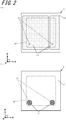
Figs. 2(a) and 2(b) are top views of an inside of the electronic device illustrated inFig. 1 . -
Fig. 3(a) is a longitudinal sectional view taken along line A-A of the electronic device illustrated inFig. 1(a) andFig. 3(b) is a longitudinal sectional view taken along line B-B. -
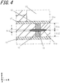
Fig. 4 is an enlarged sectional view of a main portion in portion A of the electronic device illustrated inFig. 3(b) . -
Fig. 5 is a longitudinal sectional view illustrating an electronic module using the electronic device inFig. 1 mounted on a module substrate. -
Fig. 6 is an enlarged sectional view of a main portion in another example of the electronic device in the first embodiment. -
Fig. 7(a) is a top view illustrating an electronic device in a second embodiment andFig. 7(b) is a bottom view ofFig. 7(a) . -
Figs. 8(a) and 8(b) are top views of an inside of the electronic device illustrated inFig. 7 . -
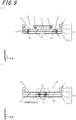
Fig. 9(a) is a longitudinal sectional view taken along line A-A of the electronic device illustrated inFig. 7(a) andFig. 9(b) is a longitudinal sectional view taken along line B-B. -
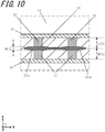
Fig. 10 is an enlarged sectional view of a main portion in portion A of the electronic device illustrated inFig. 9(b) . -
Fig. 11(a) is a sectional view in another example of the electronic device in the second embodiment andFig. 11(b) is an enlarged sectional view of a main portion in portion A ofFig. 11(a) . -
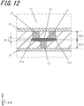
Fig. 12 is an enlarged sectional view of a main portion in an electronic device in a third embodiment. - Several exemplary embodiments of the present disclosure will be described with reference to the accompanying drawings.
- As illustrated in
Figs. 1 to 5 , an electronic device according to a first embodiment includes an electroniccomponent mounting substrate 1 and anelectronic component 2 mounted on arecess portion 14 of the electroniccomponent mounting substrate 1. As illustrated inFig. 5 , the electronic device is connected to, for example, a module substrate 4 constituting an electronic module by usingsolder 5. - The electronic
component mounting substrate 1 in the first embodiment includes aninsulating substrate 11 for mounting theelectronic component 2, avia conductor 12 positioned in theinsulating substrate 11 in a thickness direction, and avia pad conductor 13 positioned in theinsulating substrate 11, connected to thevia conductor 12, having a thickness that gradually increases from an outer edge portion toward an inside portion, and including a protruding portion 13a that protrudes from thevia conductor 12 in a width direction of thevia conductor 12. Theinsulating substrate 11 has arecess portion 14 for mounting theelectronic component 2 on one main surface, andconductor layers 15 are positioned on a surface and an inside of therecess portion 14. InFigs. 1 to 4 , an upward direction refers to a positive direction of a virtual z axis. A distinction between top and bottom in the following description is for convenience, and there is no intention to restrict the top and bottom if the electroniccomponent mounting substrate 1 or the like is actually used. - In the example illustrated in
Fig. 1 , theconductor layers 15 are indicated by shading, if viewed in a plan view, and a portion overlapping a side surface of thevia conductor 12 is indicated by a dotted line. In the example illustrated inFig. 2 , thevia conductor pad 13 and theconductor layer 15 are indicated by shading, if viewed in a plan view, and a portion overlapping the side surface of thevia conductor 12 and a portion overlapping an inner wall of therecess portion 14 are indicated by dotted lines. - The
insulating substrate 11 has one main surface (upper surface inFigs. 1 to 4 ), the other main surface (lower surface inFigs. 1 to 4 ) opposite to the main surface, and a side surface. Theinsulating substrate 11 is configured of a plurality of insulating layers 11a, is open to the main surface, and has therecess portion 14 for mounting theelectronic component 2. Theinsulating substrate 11 has a shape of a rectangular plate, if viewed in a plan view, that is, viewed in a direction perpendicular to the main surface. Theinsulating substrate 11 functions as a support for supporting theelectronic component 2, and theelectronic component 2 is bonded and fixed to a mounting portion on a bottom surface of therecess portion 14, via aconnection member 3 such as solder bump, gold bump, conductive resin (anisotropic conductive resin, or the like), or resin. - For the
insulating substrate 11, for example, ceramics such as an aluminum oxide sintered body (alumina ceramics), an aluminum nitride sintered body, a silicon nitride sintered body, a mullite sintered body, or a glass ceramic sintered body can be used. If theinsulating substrate 11 is, for example, the aluminum oxide sintered body, an appropriate organic binder and a solvent are added and mixed to a raw material powder such as aluminum oxide (Al2O3), silicon oxide (SiO2), magnesium oxide (MgO), or calcium oxide (CaO), and the like to product a slurry. A ceramic green sheet is produced by forming the slurry in a sheet form by using a well-known doctor blade method, a calendar roll method, or the like of the related art. Next, an appropriate punching process is performed on the ceramic green sheet, and a plurality of ceramic green sheets is laminated to form a green body, and the green body is fired at a high temperature (approximately 1,600°C), whereby theinsulating substrate 11 is produced. - In the example illustrated in
Figs. 1 and2 , therecess portion 14 is positioned on the main surface of theinsulating substrate 11. Therecess portion 14 is for mounting theelectronic component 2 on the bottom surface. In the example illustrated inFig. 1 , therecess portion 14 has a rectangular shape with a corner having a round shape, if viewed in a plan view, and is positioned at a center portion of theinsulating substrate 11. In the example illustrated inFigs. 1 to 3 , theinsulating substrate 11 is formed of four insulating layers 11a, and therecess portion 14 is positioned in first and second insulating layers 11a on one main surface side. Between the bottom surface of therecess portion 14 and the other main surface of theinsulating substrate 11, two insulating layers 11a are formed. The example illustrated inFig. 2(a) is a top view of an inside of the bottom surface on therecess portion 14, that is, a third insulating layer 11a on the one main surface side, if viewed in a plan view. The example illustrated inFig. 2(b) is a top view of an inside between the bottom surface of therecess portion 14 of therecess portion 14 and the other main surface of theinsulating substrate 11, that is, of a fourth insulating layer 11a on the one main surface side, if viewed in a plan view. - The
recess portion 14 can be formed, for example, by forming a through-hole to be therecess portion 14 in each ceramic green sheet by a laser process, a punching with a mold in a portion of the ceramic green sheets for theinsulating substrate 11, and laminating the ceramic green sheets on other ceramic green sheets in which no through-hole is formed. - The
via conductors 12, thevia pad conductors 13, and theconductor layers 15 are positioned on the surface and the inside of theinsulating substrate 11. Thevia conductors 12, thevia pad conductors 13, and theconductor layers 15 are for electrically connecting theelectronic component 2 and the module substrate 4. As in the example illustrated inFigs. 1 to 3 , theconductor layers 15 are positioned on the bottom surface of therecess portion 14 and the other main surface of theinsulating substrate 11. Thevia conductor 12 is positioned in theinsulating substrate 11 in the thickness direction (z direction inFigs. 1 to 3 ), and an end portion of thevia conductor 12 is connected to theconductor layer 15. Thevia pad conductor 13 is positioned in theinsulating substrate 11, and is positioned between thevia conductor 12 on a bottom surface side of therecess portion 14 and thevia conductor 12 on the other main surface side of theinsulating substrate 11. The upper surface and the lower surface of the via pad conductor are respectively connected to thevia conductors 12. - As in the example illustrated in
Figs. 1 to 3 , thevia conductor 12 is positioned so as to overlap therecess portion 14, if viewed in a plan view. As in the example illustrated inFigs. 3 and4 , thevia conductors 12 are positioned in at least two insulating layers 11a respectively in the thickness direction of theinsulating substrate 11 between the bottom surface of therecess portion 14 and the other main surface of theinsulating substrate 11. Thevia conductor 12 on the bottom surface side of therecess portion 14 and thevia conductor 12 on the other main surface side of theinsulating substrate 11 overlap each other, if viewed in a plan view, that is, are positioned vertically in the thickness direction from the bottom surface of therecess portion 14 to the other main surface of theinsulating substrate 11, if viewed in a longitudinal sectional view. - As in the example illustrated in
Figs. 3 and4 , thevia pad conductor 13 gradually increases in thickness from the outer edge portion toward the center portion and has the protruding portion 13a extending from thevia conductor 12 in the width direction of thevia conductor 12. As illustrated in the example inFigs. 1 to 3 , the protruding portion 13a of thevia pad conductor 13 extends from each of thevia conductor 12 connected to the upper surface of thevia pad conductor 13 and thevia conductor 12 connected to the lower surface thereof in the width direction of thevia conductor 12. The width direction of thevia conductor 12 is any direction of a width (diameter) of thevia conductor 12 in a planar direction, if viewed in a plan view. The protruding portion 13a extending from thevia conductor 12 in the width direction of thevia conductor 12 means that the protruding portion 13a of thevia pad conductor 13 extends to an outside beyond the side surface of thevia conductor 12, if viewed in a plan view. In the example illustrated inFigs. 1 to 3 , thevia pad conductor 13 has the protruding portion 13a extending from thevia conductor 12 over an entire periphery of the side surface of thevia conductor 12. - The
via conductor 12, thevia pad conductor 13, and theconductor layer 15 are, for example, formed by metallization of metal powder mainly composed of tungsten (W), molybdenum (Mo), manganese (Mn), silver (Ag), copper (Cu), or the like. For example, if theinsulating substrate 11 is made of the aluminum oxide sintered body, a metallized paste obtained by adding and mixing an appropriate organic binder and a solvent or the like to a high-melting-point metal powder such as W, Mo, or Mn is preliminarily printed and applied to the ceramic green sheet for the insulatingsubstrate 11 in a predetermined pattern by a screen printing method, and is fired at the same time as the ceramic green sheet for theinsulating substrate 11 to be deposited and formed at a predetermined position of theinsulating substrate 11. The viapad conductor 13 and theconductor layer 15 are formed by, for example, printing and applying a metallized paste for the viapad conductor 13 and theconductor layer 15 on the ceramic green sheet for the insulatingsubstrate 11 by printing means such as a screen printing method, and firing the metallized paste together with the ceramic green sheet for the insulatingsubstrate 11. The viaconductor 12 is formed, for example, by forming a through-hole for the viaconductor 12 in the ceramic green sheet for the insulatingsubstrate 11 by a processing method such as a punching with a mold, or a laser process, filling the through-hole with the metallized paste for the viaconductor 12 by the printing means, and firing the metallized paste together with the ceramic green sheet for the insulatingsubstrate 11. The metallized paste is produced by appropriately adjusting the viscosity by adding an appropriate solvent and binder to the metal powder described above and kneading. In order to increase a bonding strength with the insulatingsubstrate 11, glass powder or ceramic powder may be included. - As in the example illustrated in
Figs. 3 and4 , the viapad conductor 13 gradually increases in thickness from the outer edge portion toward the inside portion. The viapad conductor 13 can be formed, for example, by making the thickness of the inside greater than the thickness of the outer edge portion side, if the metallized paste for the viapad conductor 13 is printed on the surface of the ceramic green sheet, on the metallized paste for the viaconductor 12, with which the through-hole for the viaconductor 12 formed in the ceramic green sheet for the insulatingsubstrate 11 is filled. - A metal plating layer is deposited on the surface of the
conductor layer 15 exposed from the insulatingsubstrate 11 by an electroplating method or an electroless plating method. The metal plating layer is made of metal having good corrosion resistance and good connection member connectivity, such as nickel, copper, gold, or silver. For example, a nickel plating layer having a thickness of approximately 0.5 to 5 µm and a gold plating layer having a thickness of approximately 0.1 to 3 µm are deposited sequentially. Therefore, the corrosion of theconductor layer 15 can be effectively suppressed, bonding between theconductor layer 15 and theconnection member 3 such as a bonding wire, and bonding between theconductor layer 15 and aconnection pad 41 for connection positioned on the module substrate 4 can be strengthened. - The metal plating layer is not limited to the nickel plating layer/gold plating layer, and may be other metal plating layers including a nickel plating layer/palladium plating layer/gold plating layer, and the like.
- The electronic device can be produced by mounting the
electronic component 2 on the bottom surface of therecess portion 14 of the electroniccomponent mounting substrate 1. Theelectronic component 2 for mounting on the electroniccomponent mounting substrate 1 is a semiconductor element such as an IC chip or an LSI chip, a light emitting element, a piezoelectric element such as a crystal oscillator or a piezoelectric vibrator, or various sensors. For example, if theelectronic component 2 is a wire-bonding-type semiconductor element, the semiconductor element is fixed to the bottom surface of therecess portion 14 with a bonding member such as a low-melting-point brazing material or a conductive resin, and then the electrode of the semiconductor element and theconductor layer 15 are electrically connected via theconnection member 3 such as a bonding wire, and thereby the semiconductor element is mounted on the electroniccomponent mounting substrate 1. Thus, theelectronic component 2 is electrically connected to theconductor layer 15. For example, if theelectronic component 2 is a flip-chip-type semiconductor element, the electrode of the semiconductor element and theconductor layer 15 are electrically and mechanically connected to each other via theconnection member 3 such as a solder bump, a gold bump, or a conductive resin (anisotropic conductive resin or the like), and thereby the semiconductor element is mounted on the electroniccomponent mounting substrate 1. A plurality ofelectronic components 2 may be mounted on the bottom surface of therecess portion 14 of the electroniccomponent mounting substrate 1, or a small electronic component such as a resistor element or a capacitor element may be mounted, as necessary. Theelectronic component 2 is sealed by using a sealing material made of resin, glass, or the like, or a lid made of resin, glass, ceramics, metal, or the like, as necessary. - For example, as illustrated in
Fig. 4 , theconductor layer 15 of the electronic device of the present embodiment is connected to theconnection pad 41 of the module substrate 4 via thesolder 5 to form the electronic module. In the electronic device, for example, as illustrated inFig. 4 , theconductor layer 15 positioned on the other main surface of the electroniccomponent mounting substrate 1 is connected to theconnection pad 41 of the module substrate 4. - The electronic
component mounting substrate 1 of the present embodiment includes the insulatingsubstrate 11 for mounting theelectronic component 2, the viaconductor 12 positioned in the insulatingsubstrate 11 in the thickness direction, and the viapad conductor 13 positioned in the insulatingsubstrate 11, connected to the viaconductor 12, having a thickness that gradually increases from the outer edge portion toward the inside portion, and including the protruding portion 13a protruding from the viaconductor 12 in the width direction of the viaconductor 12. With the configuration described above, for example, even if the stress is applied to the electronic device including the electroniccomponent mounting substrate 1 in a planar direction and the stress is applied to the viaconductor 12 by an external force during handling, the stress is dispersed by the viapad conductor 13 of which the thickness gradually increases from the outer edge portion toward the inside portion, generation of a gap between the insulatingsubstrate 11 and the viaconductor 12 is suppressed, and reduction of airtightness between therecess portion 14 and the lower surface of the insulatingsubstrate 11 can be suppressed. - As in the example illustrated in
Fig. 4 , if the end portion of the protruding portion 13a is pointed, for example, even if the stress is applied to the electronic device including the electroniccomponent mounting substrate 1 in the planar direction, and the stress is applied to the viaconductor 12 by an external force during handling, the stress is further dispersed by the viapad conductor 13 having a larger inclined surface from the outer edge portion toward the inside portion, and generation of the gap between the insulatingsubstrate 11 and the viaconductor 12 is further suppressed, and reduction of the airtightness between therecess portion 14 and the lower surface of the insulatingsubstrate 11 can be suppressed. Sharpness indicates that the thickness of the viapad conductor 13 is reduced, if viewed in a longitudinal sectional view. - If the protruding portion 13a of the via
pad conductor 13 protrudes from the viaconductors 12 over an entire periphery of the side surface of the viaconductors 12 in the width direction, which are connected to the upper surface and the lower surface, the stress is dispersed by the viapad conductor 13 over the entire periphery of the side surface of the viaconductors 12 in the width direction, generation of the gap between the insulatingsubstrate 11 and the viaconductors 12 is suppressed, and reduction of the airtightness between therecess portion 14 and the lower surface of the insulatingsubstrate 11 can be suppressed. - As in the example illustrated in
Figs. 3 and4 , if the thickness of the center portion of the viapad conductor 13 is larger than the thickness of the outer edge portion thereof, if viewed in a longitudinal sectional view, for example, even if the stress in the planar direction is applied to the electronic device including the electroniccomponent mounting substrate 1 and the stress is applied to the viaconductor 12 by the external force during handling, the stress is dispersed by the viapad conductor 13 of which the thickness of the center portion is larger than the thickness of the outer edge portion. Further, in the insulatingsubstrate 11, the stress is effectively dispersed at a portion that is in contact from the center portion to the outer edge portion of the viapad conductor 13, generation of the gap between the insulatingsubstrate 11 and the viaconductor 12 is suppressed, and reduction of the airtightness between therecess portion 14 and the lower surface of the insulatingsubstrate 11 can be suppressed. - As illustrated in
Fig. 4 , thicknesses H11 and H12 of the respective insulating layers 11a where the viaconductors 12 are positioned across the viapad conductor 13 may be within ±10% of one insulating layer 11a (0.9H12 ≤ H11 ≤ 1.1H12). In this case, the stress applied to each viaconductor 12 is easily dispersed evenly between the bottom surface side of therecess portion 14 and the lower surface side of the insulatingsubstrate 11. Therefore, generation of the gap between the insulatingsubstrate 11 and the viaconductor 12 on the bottom surface side of therecess portion 14, and between the insulatingsubstrate 11 and the viaconductor 12 on the lower surface side of the insulatingsubstrate 11 is further suppressed, and reduction of the airtightness between therecess portion 14 and the lower surface of the insulatingsubstrate 11 can be suppressed. - If (0.9H12 ≤ H11 ≤ 1.1H12) described above is satisfied, if a maximum thickness H2 of the via
pad conductor 13 is equal to or greater than a difference between the thicknesses H11 and H12 (H2 ≥ |H11-H12|) of the respective insulating layers 11a where the viaconductors 12 are positioned across the viapad conductor 13, the thickness gradually increases and well positioned from the outer edge portion to the inside portion on the bottom surface side of therecess portion 14 and the lower surface side of the insulatingsubstrate 11, and the stress applied to respective viaconductors 12 is easily and evenly dispersed on the bottom surface side of therecess portion 14 and the lower surface side of the insulatingsubstrate 11. Therefore, generation of the gap between the insulatingsubstrate 11 and the viaconductor 12 on the bottom surface side of therecess portion 14, and between the insulatingsubstrate 11 and the viaconductor 12 on the lower surface side of the insulatingsubstrate 11 is further suppressed, and reduction of the airtightness between therecess portion 14 and the lower surface of the insulatingsubstrate 11 can be suppressed. - If one end portion of the via
conductor 12 in the width direction and the protruding portion 13a are in contact with each other, if for example, the stress is applied to the electronic device including the electroniccomponent mounting substrate 1 in the planar direction and the stress is applied to the viaconductor 12 by the external force during handling and a gap may easily be generated between the insulatingsubstrate 11 and the viaconductor 12, the airtightness is easily maintained at a portion where the one end portion of the viaconductor 12 in the width direction is in contact with the protruding portion 13a, the protruding portion 13a, and a portion where the protruding portion 13a is in contact with the insulatingsubstrate 11. Thus, reduction of the airtightness between therecess portion 14 and the lower surface of the insulatingsubstrate 11 can be suppressed. - If both end portions of the via
conductor 12 in the width direction are in contact with the protruding portion 13a, if for example, the stress is applied to the electronic device including the electroniccomponent mounting substrate 1 in the planar direction and the stress is applied to the viaconductor 12 by the external force during handling and a gap may easily be generated between the insulatingsubstrate 11 and the both end portions of the viaconductor 12 in the width direction, the airtightness is further easily maintained at a portion where the both end portions of the viaconductor 12 in the width direction are in contact with the protruding portion 13a, the protruding portion 13a, and a portion where the protruding portion 13a is in contact with the insulatingsubstrate 11. Thus, reduction of the airtightness between therecess portion 14 and the lower surface of the insulatingsubstrate 11 can be suppressed. The outer edge of the entire periphery of the viaconductor 12 in the width direction may be connected to the protruding portion 13a. - As in the example illustrated in
Fig. 6 , if an inclination of a contact surface between the viaconductor 12 and the viapad conductor 13 is larger than an inclination of a contact surface between the insulating layer 11a and the viapad conductor 13, for example, even if the stress is applied to the electronic device including the electronic component mounting substrate in the planar direction and the stress is applied to the via conductor by the external force during handling, the stress is effectively dispersed by the via pad conductor in which the inclination of the contact surface between the viaconductor 12 and the viapad conductor 13 is large. Thus, generation of the gap between the insulating substrate and the via conductor is effectively suppressed, and reduction of the airtightness between therecess portion 14 and the lower surface of the insulatingsubstrate 11 can be suppressed. The inclination of the contact surface between the viaconductor 12 and the viapad conductor 13 may be larger than the inclination of the contact surface between the insulating layer 11a and the viapad conductor 13, and the protruding portion 13a may be connected, at the outer edge of the entire periphery of the viaconductor 12 in the width direction. - For example, such via
conductors 12 and viapad conductors 13 can be formed as follows. If the through-hole for the viaconductor 12 in the ceramic green sheet for the insulatingsubstrate 11 is filled with the metallized paste for the viaconductor 12, an opening of the through-hole for the viaconductor 12 is filled with the metallized paste for the viaconductor 12 so that a sectional view has a recessed-curved surface shape (shape that is recessed from the outer edge portion of the opening toward the center portion of the opening), and the through-hole for the viaconductor 12 is filled with the metallized paste for the viapad conductor 13 on the metallized paste for the viaconductor 12, whereby the viaconductors 12 and the viapad conductors 13 are formed on the surface of the ceramic green sheet by printing. - If the via
conductor 12 and the viapad conductor 13 contain the same ceramic as the insulatingsubstrate 11, the content ratio of ceramic contained in the viapad conductor 13 may be higher than the content ratio of ceramic contained in the viaconductor 12. For example, the content ratio of ceramic contained in the viapad conductor 13 may be as high as approximately 1.2 to 2 times the content ratio of ceramic contained in the viaconductor 12. Therefore, a resistance difference between the viapad conductor 13 and the viaconductor 12 having a smaller area, if viewed in a plan view, than that of the viapad conductor 13 is reduced, the contact between the viaconductor 12 and the viapad conductor 13 is good, and a shift between the viaconductor 12 and the viapad conductor 13 is suppressed. Therefore, reduction of the airtightness between therecess portion 14 and the lower surface of the insulatingsubstrate 11 can be suppressed. - The electronic device according to the present embodiment includes the electronic
component mounting substrate 1 having the configuration described above, and theelectronic component 2 mounted on the electroniccomponent mounting substrate 1, and thereby an electronic device having good long-term reliability can be obtained. - The electronic module of the present embodiment includes the module substrate 4 having the
connection pad 41 and the electronic device having the configuration described above connected to theconnection pad 41 via thesolder 5, and thereby having good long-term reliability. - The electronic
component mounting substrate 1 in the present embodiment can be suitably used in a thin and high-power electronic device. In particular, the electroniccomponent mounting substrate 1 can be suitably used if the diameter of the viaconductor 12 is smaller than a height of the viaconductor 12. For example, if a light emitting element such as an LED is mounted as theelectronic component 2 on the bottom surface of therecess portion 14, the airtightness of therecess portion 14 is good and the electroniccomponent mounting substrate 1 can be suitably used as the electroniccomponent mounting substrate 1 for a thin and high-luminance light emitting device. - Next, an electronic device according to a second embodiment will be described with reference to
Figs. 7 to 10 . - The electronic device according to the second embodiment is different from the electronic device according to the embodiment described above in that a plurality of via
conductors 12 is connected to an upper surface and a lower surface of one viapad conductor 13, respectively. In the example illustrated inFigs. 7 to 10 , two viaconductors 12 are connected to the upper surface of one viapad conductor 13, and two viaconductors 12 are connected to the lower surface of one viapad conductor 13. - In the example illustrated in
Fig. 7 , the conductor layers 15 are indicated by shading, if viewed in a plan view, and a portion overlapping a side surface of the viaconductor 12 is indicated by a dotted line. In the example illustrated inFig. 8 , the viaconductor pads 13 and the conductor layers 15 are indicated by shading, and a portion overlapping the side surface of the viaconductor 12 and a portion overlapping an inner wall of therecess portion 14 are indicated by dotted lines. - According to the electronic
component mounting substrate 1 of the second embodiment, similarly to the electroniccomponent mounting substrate 1 of the first embodiment, for example, even if the stress in the planar direction is applied to an electronic device including the electroniccomponent mounting substrate 1 and the stress is applied to the individual viaconductors 12 by an external force during handling, the stress is dispersed by the via pad conductor of which the thickness gradually increases from the outer edge portion toward the inside portion, generation of a gap between the insulatingsubstrate 11 and the individual viaconductors 12 is suppressed, and reduction of the airtightness between therecess portion 14 and the lower surface of the insulatingsubstrate 11 can be suppressed. - In the example illustrated in
Fig. 10 , in the electroniccomponent mounting substrate 1 according to the second embodiment, a thickness of the viapad conductor 13 between the plurality of viaconductors 12, if viewed in a longitudinal sectional view is smaller than a thickness of the viapad conductor 13 in a region overlapping the viaconductors 12, if viewed in a plan view. In the electroniccomponent mounting substrate 1 according to the second embodiment, the viapad conductor 13 connected to the plurality of viaconductors 12 includes protruding portion 13a protruding from the plurality of viaconductors 12 in the width direction of the viaconductor 12. As in the examples illustrated inFigs. 7 to 10 , the protruding portion 13a of the viapad conductor 13 extends from each of the plurality of viaconductors 12 connected to the upper surface of the viapad conductor 13 and the plurality of viaconductors 12 connected to the lower surface thereof in the width direction of the viaconductor 12. - If the protruding portion 13a of the via
pad conductor 13 protrudes from each viaconductor 12 over an entire periphery of the side surface in the width direction of the plurality of the viaconductors 12 connected to the upper surface and the lower surface, the stress is dispersed by the viapad conductor 13 over the entire periphery of the side surface of the viaconductors 12 in the width direction, generation of the gap between the insulatingsubstrate 11 and the viaconductor 12 is suppressed, and reduction of the airtightness between therecess portion 14 and the lower surface of the insulatingsubstrate 11 can be suppressed. - As in the example illustrated in
Fig. 11 , the thickness of the viapad conductor 13 between the plurality of viaconductors 12 if viewed in a plan view may be larger than the thickness of the viapad conductor 13 in a region overlapping the viaconductors 12, if viewed in a sectional view. - The electronic
component mounting substrate 1 of the second embodiment can be produced by using the same producing method as that of the electroniccomponent mounting substrate 1 of the embodiment described above. - Similarly to the electronic
component mounting substrate 1 of the first embodiment, the electroniccomponent mounting substrate 1 of the second embodiment can be suitably used in a thin and high-power electronic device. In particular, the electroniccomponent mounting substrate 1 can be suitably used if the diameter of the viaconductor 12 is smaller than a height of the viaconductor 12. For example, if a light emitting element such as an LED is mounted as theelectronic component 2 on the bottom surface of therecess portion 14, the airtightness of therecess portion 14 is good and the electroniccomponent mounting substrate 1 can be suitably used as the electroniccomponent mounting substrate 1 for a thin and high-luminance light emitting device. - Next, an electronic device according to a third embodiment will be described with reference to
Fig. 12 . - The electronic device according to the third embodiment is different from the electronic device according to the embodiments described above in that the number of via
conductors 12 connected to the upper surface of one viapad conductor 13 is different from the number of viaconductors 12 connected to the lower surface of one viapad 13. In the example illustrated inFig. 12 , two viaconductors 12 are connected to the upper surface of one viapad conductor 13, and one viaconductor 12 is connected to the lower surface of the one viapad conductor 13. - According to the electronic
component mounting substrate 1 of the third embodiment, similarly to the electroniccomponent mounting substrate 1 of the first embodiment, for example, even if the stress in the planar direction is applied to an electronic device including the electroniccomponent mounting substrate 1 and the stress is applied to the viaconductor 12 by an external force during handling, the stress is dispersed by the viapad conductor 13 of which the thickness gradually increases from the outer edge portion toward the inside portion, generation of a gap between the insulatingsubstrate 11 and the viaconductors 12 is suppressed. In addition, the viaconductor 12 on the bottom surface side of therecess portion 14 and the viaconductor 12 on the lower surface side of the insulatingsubstrate 11 are positioned not to overlap each other across the viapad conductor 13, if viewed in a plan view, so that the stress applied to the viapad conductor 13 is dispersed in the planar direction, and reduction of the airtightness between therecess portion 14 and the lower surface of the insulatingsubstrate 11 can be effectively suppressed. - As in the example illustrated in
Fig. 12 , each viaconductor 12 connected to the lower surface of one viapad 13 is positioned between the viaconductors 12 connected to the upper surface of one viapad conductor 13, if viewed in a longitudinal sectional view. The viaconductors 12 connected to the upper surface of one viapad conductor 13 and each viaconductor 12 connected to the lower surface of one viapad 13 are positioned so as not to overlap each other, if viewed in a plan view. - In the electronic
component mounting substrate 1 according to the third embodiment, the viapad conductor 13 connected to the plurality of viaconductors 12 includes the protruding portions 13a protruding from the plurality of viaconductors 12 in the width direction of the viaconductors 12. As in the example illustrated inFig. 12 , the protruding portion 13a of the viapad conductor 13 extends from each of the plurality of viaconductors 12 connected to the upper surface of the viapad conductor 13 and the viaconductor 12 connected to the lower surface thereof in the width direction of the viaconductor 12. - If the protruding portion 13a of the via
pad conductor 13 protrudes from each viaconductor 12 over an entire periphery of the side surface in the width direction of the plurality of the viaconductors 12 connected to the upper surface and the lower surface, the stress is dispersed by the viapad conductor 13 over the entire periphery of the side surface of the viaconductors 12 in the width direction, generation of the gap between the insulatingsubstrate 11 and the viaconductor 12 is suppressed, and reduction of the airtightness between therecess portion 14 and the lower surface of the insulatingsubstrate 11 can be suppressed. - The electronic
component mounting substrate 1 of the third embodiment can be produced by using the same producing method as that of the electroniccomponent mounting substrate 1 of the embodiments described above. - Similarly to the electronic
component mounting substrate 1 of the first embodiment, the electroniccomponent mounting substrate 1 of the third embodiment can be suitably used in a thin and high-power electronic device. In particular, the electroniccomponent mounting substrate 1 can be suitably used if the diameter of the viaconductor 12 is smaller than a height of the viaconductor 12. For example, if a light emitting element such as an LED is mounted as theelectronic component 2 on the bottom surface of therecess portion 14, the airtightness of therecess portion 14 is good and the electroniccomponent mounting substrate 1 can be suitably used as the electroniccomponent mounting substrate 1 for a thin and high-luminance light emitting device. - The present disclosure is not limited to the examples of the embodiments described above, and various modifications are possible. For example, the insulating
substrate 11 may have a rectangular shape including a notch portion or a chamfered portion on a side surface or at a corner, if viewed in a plan view. A notch may be positioned from the side surface of the insulatingsubstrate 11 to the other main surface, and a conductor connected to theconductor layer 15 and positioned on an inner surface of the notch, that is, a castellation conductor may be included. - In the electronic
component mounting substrates 1 according to the first to third embodiments, the inner wall surface of therecess portion 14 is positioned perpendicular to the bottom surface of therecess portion 14, if viewed in a sectional view. However, the inner wall surface of therecess portion 14 may be an inclined surface so that, in the inner wall surface of therecess portion 14, an opening side is wider than a bottom surface side of therecess portion 14. A metal layer may be positioned on the inner wall surface of therecess portion 14. For example, if a light emitting element is used as theelectronic component 2, if a metal layer having good reflectance is positioned on the inner wall surface of therecess portion 14, the electroniccomponent mounting substrate 1 can be suitably used as the electroniccomponent mounting substrate 1 for a light emitting device having good light emission luminance. - In the electronic
component mounting substrates 1 of the first to third embodiments, embodiments may be combined. For example, in the electroniccomponent mounting substrate 1 of the second embodiment or the electroniccomponent mounting substrate 1 of the third embodiment, as in the example illustrated in the electroniccomponent mounting substrate 1 of the first embodiment, the inclination of the contact surface between the viaconductor 12 and the viapad conductor 13 may be larger than the inclination of the contact surface between the insulating layer 11a and the viapad conductor 13. - In the electronic
component mounting substrates 1 of the first to third embodiments, therecess portion 14 has a substantially rectangular shape, if viewed in a plan view, but may have another shape such as a circular shape, if viewed in a plan view. - In the embodiments described above, an example, in which the insulating
substrate 11 is configured of four insulating layers 11a, is illustrated. However, the insulatingsubstrate 11 may be configured of two, three, or five or more insulating layers 11a. Therecess portion 14 may be arecess portion 14 of which an inner wall surface is stepped, if viewed in a longitudinal sectional view. - The electronic
component mounting substrates 1 of the first to third embodiments have therecess portion 14 positioned on one main surface, but may not have a recess portion, that is, the electroniccomponent mounting substrate 1 having a flat insulatingsubstrate 11 may be provided. In this case, if a frame or a lid having a frame portion is bonded to one main surface of the electroniccomponent mounting substrate 1, the airtightness between the one main surface of the insulatingsubstrate 11 and the other main surface of the insulatingsubstrate 11 can be improved. - The electronic
component mounting substrate 1 may be produced in a form of a multi-piece substrate.
Claims (7)
- An electronic component mounting substrate comprising:an insulating substrate for mounting an electronic component;a via conductor disposed in the insulating substrate in a thickness direction of the insulating substrate; anda via pad conductordisposed in the insulating substrate,connected to the via conductor,having a thickness gradually increasing from an outer edge portion toward an inside portion, andcomprising a protruding portion protruding from the via conductor in a width direction of the via conductor.
- The electronic component mounting substrate according to claim 1, wherein
an end portion of the protruding portion is pointed. - The electronic component mounting substrate according to claim 1 or 2, wherein
a thickness of a center portion of the via pad conductor is larger than a thickness of an outer edge portion of the via pad conductor. - The electronic component mounting substrate according to any one of claims 1 to 3, wherein
one end portion of the via conductor in the width direction is in contact with the protruding portion. - The electronic component mounting substrate according to any one of claims 1 to 3, wherein
both end portions of the via conductor in the width direction are in contact with the protruding portion. - An electronic device comprising:the electronic component mounting substrate according to any one of claims 1 to 5; andan electronic component mounted on the electronic component mounting substrate.
- An electronic module comprising:a module substrate comprising a connection pad; andthe electronic device according to claim 6 connected to the connection pad via solder to the external electrode.
Applications Claiming Priority (2)
| Application Number | Priority Date | Filing Date | Title |
|---|---|---|---|
| JP2017164453 | 2017-08-29 | ||
| PCT/JP2018/031376 WO2019044706A1 (en) | 2017-08-29 | 2018-08-24 | Substrate for mounting electronic components, electronic device, and electronic module |
Publications (3)
| Publication Number | Publication Date |
|---|---|
| EP3678196A1 true EP3678196A1 (en) | 2020-07-08 |
| EP3678196A4 EP3678196A4 (en) | 2021-05-19 |
| EP3678196B1 EP3678196B1 (en) | 2023-07-05 |
Family
ID=65527339
Family Applications (1)
| Application Number | Title | Priority Date | Filing Date |
|---|---|---|---|
| EP18851332.9A Active EP3678196B1 (en) | 2017-08-29 | 2018-08-24 | Substrate for mounting electronic components, electronic device, and electronic module |
Country Status (5)
| Country | Link |
|---|---|
| US (1) | US11004781B2 (en) |
| EP (1) | EP3678196B1 (en) |
| JP (1) | JP6933716B2 (en) |
| CN (1) | CN111033771B (en) |
| WO (1) | WO2019044706A1 (en) |
Families Citing this family (3)
| Publication number | Priority date | Publication date | Assignee | Title |
|---|---|---|---|---|
| JP7576976B2 (en) * | 2020-12-25 | 2024-11-01 | 田中貴金属工業株式会社 | Method for manufacturing an interposer substrate and a device using the interposer substrate |
| TWI742991B (en) * | 2021-01-20 | 2021-10-11 | 啟耀光電股份有限公司 | Substrate structure and electronic device |
| JP2023088622A (en) * | 2021-12-15 | 2023-06-27 | 日本碍子株式会社 | Wafer table |
Family Cites Families (11)
| Publication number | Priority date | Publication date | Assignee | Title |
|---|---|---|---|---|
| JP2003332716A (en) * | 2002-03-04 | 2003-11-21 | Ngk Spark Plug Co Ltd | Wiring board and method of manufacturing wiring board |
| JP2003298240A (en) * | 2002-04-05 | 2003-10-17 | Sohwa Corporation | Multilayer circuit board |
| JP2005011883A (en) | 2003-06-17 | 2005-01-13 | Shinko Electric Ind Co Ltd | WIRING BOARD, SEMICONDUCTOR DEVICE, AND WIRING BOARD MANUFACTURING METHOD |
| US7402758B2 (en) * | 2003-10-09 | 2008-07-22 | Qualcomm Incorporated | Telescoping blind via in three-layer core |
| US7759582B2 (en) * | 2005-07-07 | 2010-07-20 | Ibiden Co., Ltd. | Multilayer printed wiring board |
| JP2006191146A (en) * | 2006-03-20 | 2006-07-20 | Kyocera Corp | Manufacturing method of multilayer wiring board |
| US20070236895A1 (en) * | 2006-03-30 | 2007-10-11 | Bartley Gerald K | Via resistor structure and method for trimming resistance value |
| JP2014086679A (en) * | 2012-10-26 | 2014-05-12 | Kyocera Corp | Thin film wiring board, multilayer wiring board and substrate for probe card |
| JP6385075B2 (en) * | 2013-04-15 | 2018-09-05 | キヤノン株式会社 | Printed wiring board, printed circuit board, and electronic equipment |
| JP2015159245A (en) | 2014-02-25 | 2015-09-03 | 京セラ株式会社 | Package for mounting light-emitting element and light-emitting device |
| KR20160110588A (en) * | 2015-03-09 | 2016-09-22 | 삼성전기주식회사 | Semiconductor device and method for manufacturing therefor |
-
2018
- 2018-08-24 US US16/642,040 patent/US11004781B2/en active Active
- 2018-08-24 JP JP2019539454A patent/JP6933716B2/en active Active
- 2018-08-24 WO PCT/JP2018/031376 patent/WO2019044706A1/en not_active Ceased
- 2018-08-24 CN CN201880054090.9A patent/CN111033771B/en active Active
- 2018-08-24 EP EP18851332.9A patent/EP3678196B1/en active Active
Also Published As
| Publication number | Publication date |
|---|---|
| EP3678196B1 (en) | 2023-07-05 |
| WO2019044706A1 (en) | 2019-03-07 |
| CN111033771B (en) | 2023-10-20 |
| EP3678196A4 (en) | 2021-05-19 |
| JP6933716B2 (en) | 2021-09-08 |
| US20210066180A1 (en) | 2021-03-04 |
| US11004781B2 (en) | 2021-05-11 |
| JPWO2019044706A1 (en) | 2020-09-24 |
| CN111033771A (en) | 2020-04-17 |
Similar Documents
| Publication | Publication Date | Title |
|---|---|---|
| US11145587B2 (en) | Electronic component mounting substrate, electronic device, and electronic module | |
| JP2018073905A (en) | Electronic component mounting board, electronic device and electronic module | |
| EP3678196B1 (en) | Substrate for mounting electronic components, electronic device, and electronic module | |
| US10985098B2 (en) | Electronic component mounting substrate, electronic device, and electronic module | |
| JP2021184481A (en) | Electronic module | |
| JP6780996B2 (en) | Wiring boards, electronics and electronic modules | |
| US10937707B2 (en) | Wiring substrate, electronic device, and electronic module | |
| JP6698301B2 (en) | Wiring board, electronic device and electronic module | |
| US11024554B2 (en) | Wiring substrate, electronic device, and electronic module | |
| JP6737646B2 (en) | Wiring board, electronic device and electronic module | |
| JP6687435B2 (en) | Wiring board, electronic device and electronic module | |
| JP6595308B2 (en) | Electronic component mounting substrate, electronic device and electronic module | |
| JP2020181982A (en) | Wiring board, electronic apparatus, and electronic module |
Legal Events
| Date | Code | Title | Description |
|---|---|---|---|
| STAA | Information on the status of an ep patent application or granted ep patent |
Free format text: STATUS: THE INTERNATIONAL PUBLICATION HAS BEEN MADE |
|
| PUAI | Public reference made under article 153(3) epc to a published international application that has entered the european phase |
Free format text: ORIGINAL CODE: 0009012 |
|
| STAA | Information on the status of an ep patent application or granted ep patent |
Free format text: STATUS: REQUEST FOR EXAMINATION WAS MADE |
|
| 17P | Request for examination filed |
Effective date: 20200225 |
|
| AK | Designated contracting states |
Kind code of ref document: A1 Designated state(s): AL AT BE BG CH CY CZ DE DK EE ES FI FR GB GR HR HU IE IS IT LI LT LU LV MC MK MT NL NO PL PT RO RS SE SI SK SM TR |
|
| AX | Request for extension of the european patent |
Extension state: BA ME |
|
| DAV | Request for validation of the european patent (deleted) | ||
| DAX | Request for extension of the european patent (deleted) | ||
| A4 | Supplementary search report drawn up and despatched |
Effective date: 20210416 |
|
| RIC1 | Information provided on ipc code assigned before grant |
Ipc: H01L 33/62 20100101AFI20210412BHEP Ipc: H01L 23/12 20060101ALI20210412BHEP Ipc: H05K 3/46 20060101ALI20210412BHEP |
|
| GRAP | Despatch of communication of intention to grant a patent |
Free format text: ORIGINAL CODE: EPIDOSNIGR1 |
|
| STAA | Information on the status of an ep patent application or granted ep patent |
Free format text: STATUS: GRANT OF PATENT IS INTENDED |
|
| INTG | Intention to grant announced |
Effective date: 20230125 |
|
| RAP3 | Party data changed (applicant data changed or rights of an application transferred) |
Owner name: KYOCERA CORPORATION |
|
| GRAS | Grant fee paid |
Free format text: ORIGINAL CODE: EPIDOSNIGR3 |
|
| GRAA | (expected) grant |
Free format text: ORIGINAL CODE: 0009210 |
|
| STAA | Information on the status of an ep patent application or granted ep patent |
Free format text: STATUS: THE PATENT HAS BEEN GRANTED |
|
| P01 | Opt-out of the competence of the unified patent court (upc) registered |
Effective date: 20230505 |
|
| AK | Designated contracting states |
Kind code of ref document: B1 Designated state(s): AL AT BE BG CH CY CZ DE DK EE ES FI FR GB GR HR HU IE IS IT LI LT LU LV MC MK MT NL NO PL PT RO RS SE SI SK SM TR |
|
| REG | Reference to a national code |
Ref country code: CH Ref legal event code: EP |
|
| REG | Reference to a national code |
Ref country code: AT Ref legal event code: REF Ref document number: 1585656 Country of ref document: AT Kind code of ref document: T Effective date: 20230715 |
|
| REG | Reference to a national code |
Ref country code: DE Ref legal event code: R096 Ref document number: 602018052986 Country of ref document: DE |
|
| REG | Reference to a national code |
Ref country code: IE Ref legal event code: FG4D |
|
| REG | Reference to a national code |
Ref country code: LT Ref legal event code: MG9D |
|
| REG | Reference to a national code |
Ref country code: NL Ref legal event code: MP Effective date: 20230705 |
|
| REG | Reference to a national code |
Ref country code: AT Ref legal event code: MK05 Ref document number: 1585656 Country of ref document: AT Kind code of ref document: T Effective date: 20230705 |
|
| PG25 | Lapsed in a contracting state [announced via postgrant information from national office to epo] |
Ref country code: NL Free format text: LAPSE BECAUSE OF FAILURE TO SUBMIT A TRANSLATION OF THE DESCRIPTION OR TO PAY THE FEE WITHIN THE PRESCRIBED TIME-LIMIT Effective date: 20230705 |
|
| PG25 | Lapsed in a contracting state [announced via postgrant information from national office to epo] |
Ref country code: GR Free format text: LAPSE BECAUSE OF FAILURE TO SUBMIT A TRANSLATION OF THE DESCRIPTION OR TO PAY THE FEE WITHIN THE PRESCRIBED TIME-LIMIT Effective date: 20231006 |
|
| PG25 | Lapsed in a contracting state [announced via postgrant information from national office to epo] |
Ref country code: ES Free format text: LAPSE BECAUSE OF FAILURE TO SUBMIT A TRANSLATION OF THE DESCRIPTION OR TO PAY THE FEE WITHIN THE PRESCRIBED TIME-LIMIT Effective date: 20230705 |
|
| PG25 | Lapsed in a contracting state [announced via postgrant information from national office to epo] |
Ref country code: IS Free format text: LAPSE BECAUSE OF FAILURE TO SUBMIT A TRANSLATION OF THE DESCRIPTION OR TO PAY THE FEE WITHIN THE PRESCRIBED TIME-LIMIT Effective date: 20231105 |
|
| PG25 | Lapsed in a contracting state [announced via postgrant information from national office to epo] |
Ref country code: SE Free format text: LAPSE BECAUSE OF FAILURE TO SUBMIT A TRANSLATION OF THE DESCRIPTION OR TO PAY THE FEE WITHIN THE PRESCRIBED TIME-LIMIT Effective date: 20230705 Ref country code: RS Free format text: LAPSE BECAUSE OF FAILURE TO SUBMIT A TRANSLATION OF THE DESCRIPTION OR TO PAY THE FEE WITHIN THE PRESCRIBED TIME-LIMIT Effective date: 20230705 Ref country code: PT Free format text: LAPSE BECAUSE OF FAILURE TO SUBMIT A TRANSLATION OF THE DESCRIPTION OR TO PAY THE FEE WITHIN THE PRESCRIBED TIME-LIMIT Effective date: 20231106 Ref country code: NO Free format text: LAPSE BECAUSE OF FAILURE TO SUBMIT A TRANSLATION OF THE DESCRIPTION OR TO PAY THE FEE WITHIN THE PRESCRIBED TIME-LIMIT Effective date: 20231005 Ref country code: LV Free format text: LAPSE BECAUSE OF FAILURE TO SUBMIT A TRANSLATION OF THE DESCRIPTION OR TO PAY THE FEE WITHIN THE PRESCRIBED TIME-LIMIT Effective date: 20230705 Ref country code: LT Free format text: LAPSE BECAUSE OF FAILURE TO SUBMIT A TRANSLATION OF THE DESCRIPTION OR TO PAY THE FEE WITHIN THE PRESCRIBED TIME-LIMIT Effective date: 20230705 Ref country code: IS Free format text: LAPSE BECAUSE OF FAILURE TO SUBMIT A TRANSLATION OF THE DESCRIPTION OR TO PAY THE FEE WITHIN THE PRESCRIBED TIME-LIMIT Effective date: 20231105 Ref country code: HR Free format text: LAPSE BECAUSE OF FAILURE TO SUBMIT A TRANSLATION OF THE DESCRIPTION OR TO PAY THE FEE WITHIN THE PRESCRIBED TIME-LIMIT Effective date: 20230705 Ref country code: GR Free format text: LAPSE BECAUSE OF FAILURE TO SUBMIT A TRANSLATION OF THE DESCRIPTION OR TO PAY THE FEE WITHIN THE PRESCRIBED TIME-LIMIT Effective date: 20231006 Ref country code: FI Free format text: LAPSE BECAUSE OF FAILURE TO SUBMIT A TRANSLATION OF THE DESCRIPTION OR TO PAY THE FEE WITHIN THE PRESCRIBED TIME-LIMIT Effective date: 20230705 Ref country code: ES Free format text: LAPSE BECAUSE OF FAILURE TO SUBMIT A TRANSLATION OF THE DESCRIPTION OR TO PAY THE FEE WITHIN THE PRESCRIBED TIME-LIMIT Effective date: 20230705 Ref country code: AT Free format text: LAPSE BECAUSE OF FAILURE TO SUBMIT A TRANSLATION OF THE DESCRIPTION OR TO PAY THE FEE WITHIN THE PRESCRIBED TIME-LIMIT Effective date: 20230705 |
|
| PG25 | Lapsed in a contracting state [announced via postgrant information from national office to epo] |
Ref country code: PL Free format text: LAPSE BECAUSE OF FAILURE TO SUBMIT A TRANSLATION OF THE DESCRIPTION OR TO PAY THE FEE WITHIN THE PRESCRIBED TIME-LIMIT Effective date: 20230705 |
|
| REG | Reference to a national code |
Ref country code: CH Ref legal event code: PL |
|
| REG | Reference to a national code |
Ref country code: DE Ref legal event code: R097 Ref document number: 602018052986 Country of ref document: DE |
|
| PG25 | Lapsed in a contracting state [announced via postgrant information from national office to epo] |
Ref country code: LU Free format text: LAPSE BECAUSE OF NON-PAYMENT OF DUE FEES Effective date: 20230824 |
|
| PG25 | Lapsed in a contracting state [announced via postgrant information from national office to epo] |
Ref country code: SM Free format text: LAPSE BECAUSE OF FAILURE TO SUBMIT A TRANSLATION OF THE DESCRIPTION OR TO PAY THE FEE WITHIN THE PRESCRIBED TIME-LIMIT Effective date: 20230705 Ref country code: RO Free format text: LAPSE BECAUSE OF FAILURE TO SUBMIT A TRANSLATION OF THE DESCRIPTION OR TO PAY THE FEE WITHIN THE PRESCRIBED TIME-LIMIT Effective date: 20230705 Ref country code: LU Free format text: LAPSE BECAUSE OF NON-PAYMENT OF DUE FEES Effective date: 20230824 Ref country code: EE Free format text: LAPSE BECAUSE OF FAILURE TO SUBMIT A TRANSLATION OF THE DESCRIPTION OR TO PAY THE FEE WITHIN THE PRESCRIBED TIME-LIMIT Effective date: 20230705 Ref country code: DK Free format text: LAPSE BECAUSE OF FAILURE TO SUBMIT A TRANSLATION OF THE DESCRIPTION OR TO PAY THE FEE WITHIN THE PRESCRIBED TIME-LIMIT Effective date: 20230705 Ref country code: CZ Free format text: LAPSE BECAUSE OF FAILURE TO SUBMIT A TRANSLATION OF THE DESCRIPTION OR TO PAY THE FEE WITHIN THE PRESCRIBED TIME-LIMIT Effective date: 20230705 Ref country code: CH Free format text: LAPSE BECAUSE OF NON-PAYMENT OF DUE FEES Effective date: 20230831 Ref country code: MC Free format text: LAPSE BECAUSE OF FAILURE TO SUBMIT A TRANSLATION OF THE DESCRIPTION OR TO PAY THE FEE WITHIN THE PRESCRIBED TIME-LIMIT Effective date: 20230705 Ref country code: SK Free format text: LAPSE BECAUSE OF FAILURE TO SUBMIT A TRANSLATION OF THE DESCRIPTION OR TO PAY THE FEE WITHIN THE PRESCRIBED TIME-LIMIT Effective date: 20230705 |
|
| REG | Reference to a national code |
Ref country code: BE Ref legal event code: MM Effective date: 20230831 |
|
| PLBE | No opposition filed within time limit |
Free format text: ORIGINAL CODE: 0009261 |
|
| STAA | Information on the status of an ep patent application or granted ep patent |
Free format text: STATUS: NO OPPOSITION FILED WITHIN TIME LIMIT |
|
| REG | Reference to a national code |
Ref country code: IE Ref legal event code: MM4A |
|
| PG25 | Lapsed in a contracting state [announced via postgrant information from national office to epo] |
Ref country code: IT Free format text: LAPSE BECAUSE OF FAILURE TO SUBMIT A TRANSLATION OF THE DESCRIPTION OR TO PAY THE FEE WITHIN THE PRESCRIBED TIME-LIMIT Effective date: 20230705 |
|
| 26N | No opposition filed |
Effective date: 20240408 |
|
| GBPC | Gb: european patent ceased through non-payment of renewal fee |
Effective date: 20231005 |
|
| PG25 | Lapsed in a contracting state [announced via postgrant information from national office to epo] |
Ref country code: IE Free format text: LAPSE BECAUSE OF NON-PAYMENT OF DUE FEES Effective date: 20230824 |
|
| PG25 | Lapsed in a contracting state [announced via postgrant information from national office to epo] |
Ref country code: GB Free format text: LAPSE BECAUSE OF NON-PAYMENT OF DUE FEES Effective date: 20231005 |
|
| PG25 | Lapsed in a contracting state [announced via postgrant information from national office to epo] |
Ref country code: IE Free format text: LAPSE BECAUSE OF NON-PAYMENT OF DUE FEES Effective date: 20230824 Ref country code: GB Free format text: LAPSE BECAUSE OF NON-PAYMENT OF DUE FEES Effective date: 20231005 Ref country code: SI Free format text: LAPSE BECAUSE OF FAILURE TO SUBMIT A TRANSLATION OF THE DESCRIPTION OR TO PAY THE FEE WITHIN THE PRESCRIBED TIME-LIMIT Effective date: 20230705 |
|
| PG25 | Lapsed in a contracting state [announced via postgrant information from national office to epo] |
Ref country code: BE Free format text: LAPSE BECAUSE OF NON-PAYMENT OF DUE FEES Effective date: 20230831 |
|
| PGFP | Annual fee paid to national office [announced via postgrant information from national office to epo] |
Ref country code: DE Payment date: 20240702 Year of fee payment: 7 |
|
| PGFP | Annual fee paid to national office [announced via postgrant information from national office to epo] |
Ref country code: FR Payment date: 20240702 Year of fee payment: 7 |
|
| PG25 | Lapsed in a contracting state [announced via postgrant information from national office to epo] |
Ref country code: BG Free format text: LAPSE BECAUSE OF FAILURE TO SUBMIT A TRANSLATION OF THE DESCRIPTION OR TO PAY THE FEE WITHIN THE PRESCRIBED TIME-LIMIT Effective date: 20230705 |
|
| REG | Reference to a national code |
Ref country code: DE Ref legal event code: R079 Ref document number: 602018052986 Country of ref document: DE Free format text: PREVIOUS MAIN CLASS: H01L0033620000 Ipc: H10H0020857000 |
|
| PG25 | Lapsed in a contracting state [announced via postgrant information from national office to epo] |
Ref country code: BG Free format text: LAPSE BECAUSE OF FAILURE TO SUBMIT A TRANSLATION OF THE DESCRIPTION OR TO PAY THE FEE WITHIN THE PRESCRIBED TIME-LIMIT Effective date: 20230705 |
|
| PG25 | Lapsed in a contracting state [announced via postgrant information from national office to epo] |
Ref country code: CY Free format text: LAPSE BECAUSE OF FAILURE TO SUBMIT A TRANSLATION OF THE DESCRIPTION OR TO PAY THE FEE WITHIN THE PRESCRIBED TIME-LIMIT; INVALID AB INITIO Effective date: 20180824 |
|
| PG25 | Lapsed in a contracting state [announced via postgrant information from national office to epo] |
Ref country code: HU Free format text: LAPSE BECAUSE OF FAILURE TO SUBMIT A TRANSLATION OF THE DESCRIPTION OR TO PAY THE FEE WITHIN THE PRESCRIBED TIME-LIMIT; INVALID AB INITIO Effective date: 20180824 |
|
| PG25 | Lapsed in a contracting state [announced via postgrant information from national office to epo] |
Ref country code: TR Free format text: LAPSE BECAUSE OF FAILURE TO SUBMIT A TRANSLATION OF THE DESCRIPTION OR TO PAY THE FEE WITHIN THE PRESCRIBED TIME-LIMIT Effective date: 20230705 |
|
| REG | Reference to a national code |
Ref country code: DE Ref legal event code: R119 Ref document number: 602018052986 Country of ref document: DE |