EP3678184A1 - Pixel structure and oled display panel - Google Patents
Pixel structure and oled display panel Download PDFInfo
- Publication number
- EP3678184A1 EP3678184A1 EP18851242.0A EP18851242A EP3678184A1 EP 3678184 A1 EP3678184 A1 EP 3678184A1 EP 18851242 A EP18851242 A EP 18851242A EP 3678184 A1 EP3678184 A1 EP 3678184A1
- Authority
- EP
- European Patent Office
- Prior art keywords
- pixel
- sub
- pixels
- structure according
- area
- Prior art date
- Legal status (The legal status is an assumption and is not a legal conclusion. Google has not performed a legal analysis and makes no representation as to the accuracy of the status listed.)
- Pending
Links
Images



Classifications
-
- G—PHYSICS
- G09—EDUCATION; CRYPTOGRAPHY; DISPLAY; ADVERTISING; SEALS
- G09G—ARRANGEMENTS OR CIRCUITS FOR CONTROL OF INDICATING DEVICES USING STATIC MEANS TO PRESENT VARIABLE INFORMATION
- G09G3/00—Control arrangements or circuits, of interest only in connection with visual indicators other than cathode-ray tubes
- G09G3/20—Control arrangements or circuits, of interest only in connection with visual indicators other than cathode-ray tubes for presentation of an assembly of a number of characters, e.g. a page, by composing the assembly by combination of individual elements arranged in a matrix no fixed position being assigned to or needed to be assigned to the individual characters or partial characters
- G09G3/22—Control arrangements or circuits, of interest only in connection with visual indicators other than cathode-ray tubes for presentation of an assembly of a number of characters, e.g. a page, by composing the assembly by combination of individual elements arranged in a matrix no fixed position being assigned to or needed to be assigned to the individual characters or partial characters using controlled light sources
- G09G3/30—Control arrangements or circuits, of interest only in connection with visual indicators other than cathode-ray tubes for presentation of an assembly of a number of characters, e.g. a page, by composing the assembly by combination of individual elements arranged in a matrix no fixed position being assigned to or needed to be assigned to the individual characters or partial characters using controlled light sources using electroluminescent panels
- G09G3/32—Control arrangements or circuits, of interest only in connection with visual indicators other than cathode-ray tubes for presentation of an assembly of a number of characters, e.g. a page, by composing the assembly by combination of individual elements arranged in a matrix no fixed position being assigned to or needed to be assigned to the individual characters or partial characters using controlled light sources using electroluminescent panels semiconductive, e.g. using light-emitting diodes [LED]
- G09G3/3208—Control arrangements or circuits, of interest only in connection with visual indicators other than cathode-ray tubes for presentation of an assembly of a number of characters, e.g. a page, by composing the assembly by combination of individual elements arranged in a matrix no fixed position being assigned to or needed to be assigned to the individual characters or partial characters using controlled light sources using electroluminescent panels semiconductive, e.g. using light-emitting diodes [LED] organic, e.g. using organic light-emitting diodes [OLED]
-
- G—PHYSICS
- G09—EDUCATION; CRYPTOGRAPHY; DISPLAY; ADVERTISING; SEALS
- G09G—ARRANGEMENTS OR CIRCUITS FOR CONTROL OF INDICATING DEVICES USING STATIC MEANS TO PRESENT VARIABLE INFORMATION
- G09G3/00—Control arrangements or circuits, of interest only in connection with visual indicators other than cathode-ray tubes
- G09G3/20—Control arrangements or circuits, of interest only in connection with visual indicators other than cathode-ray tubes for presentation of an assembly of a number of characters, e.g. a page, by composing the assembly by combination of individual elements arranged in a matrix no fixed position being assigned to or needed to be assigned to the individual characters or partial characters
- G09G3/2003—Display of colours
-
- H—ELECTRICITY
- H10—SEMICONDUCTOR DEVICES; ELECTRIC SOLID-STATE DEVICES NOT OTHERWISE PROVIDED FOR
- H10K—ORGANIC ELECTRIC SOLID-STATE DEVICES
- H10K50/00—Organic light-emitting devices
- H10K50/80—Constructional details
-
- H—ELECTRICITY
- H10—SEMICONDUCTOR DEVICES; ELECTRIC SOLID-STATE DEVICES NOT OTHERWISE PROVIDED FOR
- H10K—ORGANIC ELECTRIC SOLID-STATE DEVICES
- H10K59/00—Integrated devices, or assemblies of multiple devices, comprising at least one organic light-emitting element covered by group H10K50/00
- H10K59/30—Devices specially adapted for multicolour light emission
- H10K59/35—Devices specially adapted for multicolour light emission comprising red-green-blue [RGB] subpixels
- H10K59/353—Devices specially adapted for multicolour light emission comprising red-green-blue [RGB] subpixels characterised by the geometrical arrangement of the RGB subpixels
-
- G—PHYSICS
- G09—EDUCATION; CRYPTOGRAPHY; DISPLAY; ADVERTISING; SEALS
- G09G—ARRANGEMENTS OR CIRCUITS FOR CONTROL OF INDICATING DEVICES USING STATIC MEANS TO PRESENT VARIABLE INFORMATION
- G09G2300/00—Aspects of the constitution of display devices
- G09G2300/04—Structural and physical details of display devices
- G09G2300/0439—Pixel structures
- G09G2300/0452—Details of colour pixel setup, e.g. pixel composed of a red, a blue and two green components
-
- G—PHYSICS
- G09—EDUCATION; CRYPTOGRAPHY; DISPLAY; ADVERTISING; SEALS
- G09G—ARRANGEMENTS OR CIRCUITS FOR CONTROL OF INDICATING DEVICES USING STATIC MEANS TO PRESENT VARIABLE INFORMATION
- G09G2300/00—Aspects of the constitution of display devices
- G09G2300/04—Structural and physical details of display devices
- G09G2300/0439—Pixel structures
- G09G2300/0465—Improved aperture ratio, e.g. by size reduction of the pixel circuit, e.g. for improving the pixel density or the maximum displayable luminance or brightness
Definitions
- This application relates to the field of display technologies, and in particular, to a pixel structure and an Organic Light-Emitting Diode (OLED) display panel including the pixel structure.
- OLED Organic Light-Emitting Diode
- An Organic Light-Emitting Diode is an active light-emitting device. Compared with a conventional Liquid Crystal Display (LCD) display, the OLED display technology does not need a backlight source and has a self-light-emitting property.
- a relatively thin organic material film layer and a relatively thin glass substrate are used in an OLED. When a current passes through, the organic material film layer emits light. Therefore, an OLED display panel can significantly save electric energy, may be manufactured to be lighter and thinner, withstand a broader temperature variation range than an LCD display screen, as well as have a larger visible angle.
- the OLED display panel is expected to become a next-generation panel display technology after the LCD, and is one of the technologies that draw most attention among the current panel display technologies.
- OLED screen body colorization methods There are many OLED screen body colorization methods.
- OLED colorization technology that is relatively mature and has been successfully mass-produced is an OLED evaporation technology.
- the OLED evaporation technology adopts a conventional RGB stripe arrangement manner is adopted for evaporation.
- a side-by-side arrangement has the best picture effect.
- Each of the sub-pixels is quadrilateral and has an independent organic light-emitting device.
- An organic light-emitting device is formed at a corresponding pixel position on an array substrate through a Fine Metal Mask (FMM) by using an evaporation film-forming, where the FMM is usually referred to as a metal mask or an evaporation mask for short.
- FMM Fine Metal Mask
- a technology for producing an OLED display panel with a high PPI (Pixel Per Inch, the number of pixels per inch) mainly focuses on a fine and mechanically stable FMM and pixel (sub-pixel) arrangement.
- FIG. 1 is a schematic diagram of a pixel arrangement of an OLED display panel in the prior art. As shown in FIG. 1 , a side-by-side pixel arrangement is used in the OLED display panel. Each pixel includes an R sub-pixel region 101, a G sub-pixel region 103, and a B sub-pixel region 105. Wherein the R sub-pixel region 101 includes an R light-emitting region 102 and an R non-light-emitting region (not numbered). The G sub-pixel region 103 includes a G light-emitting region 104 and a G non-light-emitting region (not numbered).
- the B sub-pixel region 105 includes a B light-emitting region 106 and a B non-light-emitting region (not numbered). Areas of the R, G, and B sub-pixel regions shown in FIG. 1 are respectively equal to areas of the light-emitting regions, and the R, G, and B sub-pixels are arranged in a straight line.
- a light-emitting region of each sub-pixel region includes a cathode, an anode, and an electroluminescent layer (also referred to an organic emission layer).
- the electroluminescent layer is located between the cathode and the anode and configured to generate a light of a predetermined color to implement display.
- a display panel in the prior art When a display panel in the prior art is prepared, it usually needs to perform an evaporation process for three times to separately form an electroluminescent layer of a corresponding color (red, green, or blue) in a light-emitting region of a pixel region of the corresponding color.
- a corresponding color red, green, or blue
- the FMM shown in FIG. 2 is used for evaporation in the OLED display panel shown in FIG. 1 .
- Such an FMM includes a shielded region 107 and several evaporation opening 108.
- a shielded region between two adjacent evaporation openings 108 in a same column is referred to as a bridge (a connection bridge).
- a bridge a connection bridge.
- RGB pixels can only reach up to 200 to 300 PPI, and it is difficult to achieve a high resolution display effect in this manner. With the increasing demand of users for the resolution of OLED display panel, such a side-by-side arrangement of RGB pixels cannot satisfy a design requirement of a product for a high PPI.
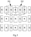
- FIG. 3 is a schematic diagram of a pixel arrangement of another OLED display panel in the prior art. As shown in FIG. 3 , only the G sub-pixel of each pixel is used separately, and each of the R and B sub-pixels is shared by adjacent pixels. For example, a pixel 201 and a pixel 202 share an R sub-pixel. Although such a method can increase a PPI of a display screen, however in this arrangement, R and B sub-pixels are shared by adjacent pixels, thus a whole display effect may include a distortion and is not a full color display in a real sense.
- a main objective of this application is to provide a pixel structure and an OLED display panel, to resolve problems existing in the prior art.
- a first aspect of embodiments of the present application provides a pixel structure, wherein the pixel structure includes a plurality of pixel groups, each of the pixel groups including a first pixel and a second pixel that are adjacent in a first direction and are disposed in a staggered manner in a second direction perpendicular to the first direction.
- Each of the first pixel and the second pixel includes sub-pixels of three different colors arranged along the second direction, and a distance between two sub-pixels of a same color respectively of the first pixel and the second pixel in the first direction is equal to that in the second direction.
- a central line of a first sub-pixel in the second pixel extending along the first direction overlaps with a borderline between a first sub-pixel and a second sub-pixel in the first pixel; or a central line of a first sub-pixel in a first pixel extending along the first direction overlaps a borderline between a first sub-pixel and a second sub-pixel in the second pixel.
- the first pixel includes a first sub-pixel, a second sub-pixel, and a third sub-pixel that are sequentially arranged along the second direction; and the second pixel includes a third sub-pixel, a first sub-pixel, and a second sub-pixel that are sequentially arranged along the second direction.
- a length-to-width ratio of an aperture of each of the sub-pixel ranges from 1 to 1.5.
- distances between centers of adjacent two sub-pixels are same.
- a shape and an area of the sub-pixels of a same color in the first pixel is same to that in the second pixel, respectively.
- the sub-pixels include a red sub-pixel, a green sub-pixel, and a blue sub-pixel.
- each of a shape and an area of the sub-pixels in the pixel group is the same.
- an area of the red sub-pixel is same to an area of the green sub-pixel, and an area of the blue sub-pixel is larger than the area of the red sub-pixel.
- the first direction is a row direction
- the second direction is a column direction
- the first direction is a column direction
- the second direction is a row direction
- a second aspect of the embodiments of the present application provides an OLED display panel, wherein the OLED display panel includes any pixel structure according to the first aspect.
- the pixel structure and OLED display panel provided by the embodiments of this application can achieve a full-color display in a real sense, and are compactly arranged so as to reduce a spacing between pixels, thus, an increased PPI is achieved by the following features: the first pixel and the second pixel are adjacently arranged along the first direction and each includes sub-pixels of three different colors; the sub-pixels are sequentially arranged along the second direction; a central line of the third sub-pixel in the second pixel extending along the first direction overlaps a borderline between the first sub-pixel and the second sub-pixel in the first pixel; a distance between two sub-pixels of a same color respectively of the first pixel and the second pixel in the first direction is equal to that in the second direction.
- one pixel can present a display effect of two pixels, thereby further improving display resolution of a screen and a manufacturing yield, and reducing difficulties in an evaporation mask manufacturing process and an evaporation process.
- a first direction is an X direction (also referred to as a row direction or a horizontal direction)
- a second direction is a Y direction (also referred to as a column direction or a vertical direction)
- the first direction is perpendicular to the second direction.
- the accompanying drawings merely show a part of a pixel structure.
- a quantity of pixels is not limited thereto, and the quantity of pixels may be varied correspondingly according to an actual display requirement.
- the first row, second row, first column, second column, and the like in this application are used for describing this application by using illustrations in the drawings as reference standards, and do not refer to rows and columns in an actual product.
- first direction and the second direction do not need to be perpendicular to each other.
- descriptions are provided below by using a case in which the first direction and the second direction are perpendicular to each other.
- a pixel structure provided by a first embodiment of this application includes a plurality of pixel groups, each of the pixel groups including a first pixel 30 and a second pixel 31 that are arranged adjacent in a first direction and are disposed in a staggered manner in a second direction, and each of the first pixel 30 and the second pixel 31 comprising sub-pixels of three different colors.
- a central line of the first sub-pixel (the sub-pixel located at an uppermost position) in the second pixel 31 extending along the first direction overlaps a borderline between the first sub-pixel and the second sub-pixel (the sub-pixel located at a middle position) in the first pixel 30.
- a central line of the first sub-pixel in the first pixel 30 extending along the first direction overlaps a borderline between the first sub-pixel and the second sub-pixel in the second pixel 31.
- the first pixel 30 includes a first sub-pixel 301, a second sub-pixel 303, and a third sub-pixel 305 that are sequentially arranged along the second direction.
- the second pixel 31 includes a third sub-pixel 311, a first sub-pixel 313, and a second sub-pixel 315 that are sequentially arranged along the second direction.
- arrangement structures of sub-pixels in the first pixel 30 and the second pixel 31 are not limited to the configurations in FIG. 4 to FIG. 8 .
- a sub-pixel arrangement may include various permutations and combinations.
- FIG. 9a and FIG. 9b show a configuration different from a configuration of FIG. 4 .
- sub-pixel arrangement structures of FIG. 4 to FIG. 8 are used for description below.
- a shape of each of the sub-pixels may be a rectangle or an oblong. No limitation is imposed in this embodiment.
- the first sub-pixel, the second sub-pixel, and the third sub-pixel in each of the first pixel 30 and the second pixel 31 include a red (R) sub-pixel, a green (G) sub-pixel, and a blue (B) sub-pixel. That is, in the embodiment of this application, the first sub-pixel is one of the red (R) sub-pixel, the green (G) sub-pixel, and the blue (B) sub-pixel; the second sub-pixel is one of the red (R) sub-pixel, the green (G) sub-pixel, and the blue (B) sub-pixel; the third sub-pixel is one of the red (R) sub-pixel, the green (G) sub-pixel, and the blue (B) sub-pixel. Colors of the first sub-pixel, the second sub-pixel, and the third sub-pixel are different from one another.
- the first sub-pixel 301 is the red (R) sub-pixel
- the second sub-pixel 303 is the green (G) sub-pixel
- the third sub-pixel 305 is the blue (B) sub-pixel. Therefore, the first sub-pixel 301 includes a red (R) light-emitting region 302 and a red (R) non-light-emitting region (not numbered in the figure), and includes an organic emission layer for emitting red light.
- the second sub-pixel 303 includes a green (G) light-emitting region 304 and a green (G) non-light-emitting region (not numbered in the figure), and includes an organic emission layer for emitting green light.
- the third sub-pixel 305 includes a blue (B) light-emitting region 306 and a blue (B) non-light-emitting region (not numbered in the figure), and includes an organic emission layer for emitting blue light.
- the first sub-pixel 313 is the red (R) sub-pixel
- the second sub-pixel 315 is the green (G) sub-pixel
- the third sub-pixel 311 is the blue (B) sub-pixel. Therefore, the first sub-pixel 313 includes a red (R) light-emitting region 314 and a red (R) non-light-emitting region (not numbered in the figure), and includes an organic emitting layer for emitting red light.
- the second sub-pixel 315 includes a green (G) light-emitting region 316 and a green (G) non-light-emitting region (not numbered in the figure), and includes an organic emitting layer for emitting green light.
- the third sub-pixel 311 includes a blue (B) light-emitting region 312 and a blue (B) non-light-emitting region (not numbered in the figure), and includes an organic emitting layer for emitting blue light.
- the shared side is the borderline between the first sub-pixel 301 and the second sub-pixel 303.
- the "border” or “borderline” described herein does not define a physical “border” or “borderline”, but may refer to a virtual “border” or “borderline” between two sub-pixels in a pixel.
- a distance between two sub-pixels of a same color that respectively of the first pixel 30 and the second pixel 31 in the first direction is equal to that in the second direction. That is, a distance between two sub-pixels of a same color in a pixel group in the first direction is equal to that in the second direction.
- a distance between an R sub-pixel of a first column and an R sub-pixel in a second column is x in a row direction and is y in a column direction, where x is equal to y.
- a distance between a G sub-pixel in the first column and a G sub-pixel in the second column is x in the row direction and is y in the column direction, where x is equal to y.
- a configuration of a B sub-pixel is similar to the above (not shown in the figure), and details are not described herein again.
- each of the pixels includes RGB three-color sub-pixels, and can achieve a full color display in a real sense.
- the pixel may be applied to a display panel with a resolution that is the same in the first direction and in the second direction or a display panel with a resolution that is different in the first direction and in the second direction.
- a pixel may present a display effect of two pixels, thereby further improving a virtual display resolution of a screen.
- the original resolution n as an example, by sharing in the first direction, the resolution of the pixel arrangement can be doubled to 2n.
- dashed-line triangles in FIG. 4 For a sharing manner, refer to dashed-line triangles in FIG. 4 . For example, in FIG.
- an R sub-pixel and a G sub-pixel in a third column are shared by B sub-pixels that are adjacent to the R sub-pixel and the G sub-pixel, in a second column and a fourth column.
- a B sub-pixel of the third column is shared by R sub-pixels and G sub-pixels that are adjacent to the B sub-pixel, in the second column and the fourth column.
- value ranges of respective aperture length-to-width ratios of two sub-pixels of a same color respectively of the first pixel 30 and the second pixel 31 are 1 to 1. 5.
- an aperture length-to-width ratio of an R sub-pixel is d:z, where a value range of d:z is 1 to 1.5.
- Configurations of a G sub-pixel and a B sub-pixel are similar to the R sub-pixel. Details are not described herein again.
- an aperture length-to-width ratio of a sub-pixel is 1.5, a design margin that can be satisfied is relatively large.
- a bridge (as shown by b in FIG. 6 and b1 in FIG. 7 ) between sub-pixels of a same color may alternatively be adjusted by adjusting a length-to-width ratio.
- a bridge value b1 in FIG. 7 is greater than a bridge value b in FIG. 6 . Therefore, compared with FIG. 6 , FIG. 7 has a higher mechanical stability, less difficulties in manufacturing process and evaporation process of a fine metal mask, and a higher manufacturing yield.
- a distance between centers of two adjacent sub-pixels is the same.
- the embodiment can enable the pixels to be arranged more compactly, reduce a spacing between pixels, and thus a PPI is increased.
- shapes and areas of two sub-pixels of a same color respectively of the first pixel 30 and the second pixel 31 are both the same. Since all sub-pixels of a same color have a same shape and a same area, manufacturing process and evaporation process difficulties for a metal mask can be further reduced. Further, shapes and areas of all sub-pixels in the pixel group may also be maintained the same.
- an area of the red sub-pixel may be the same as an area of the green sub-pixel, and an area of the blue sub-pixel may be larger than an area of the red sub-pixel.
- a second embodiment of the present application provides an OLED display panel.
- the OLED display panel includes the pixel structure according to the first embodiment.
- the first embodiment may be referred to for the pixel structure. Details are not described herein again.
- a display solution of a pixel structure in an OLED display panel is described with reference to FIG. 8 :
- a length-to-width ratio of a real pixel may be 2:1.
- the sub-pixels of each column correspondingly display a column of pixels.
- Two display driving methods may be used as follows:
Landscapes
- Engineering & Computer Science (AREA)
- Physics & Mathematics (AREA)
- Computer Hardware Design (AREA)
- General Physics & Mathematics (AREA)
- Theoretical Computer Science (AREA)
- Optics & Photonics (AREA)
- Electroluminescent Light Sources (AREA)
- Devices For Indicating Variable Information By Combining Individual Elements (AREA)
Abstract
Description
- This application relates to the field of display technologies, and in particular, to a pixel structure and an Organic Light-Emitting Diode (OLED) display panel including the pixel structure.
- An Organic Light-Emitting Diode (OLED) is an active light-emitting device. Compared with a conventional Liquid Crystal Display (LCD) display, the OLED display technology does not need a backlight source and has a self-light-emitting property. A relatively thin organic material film layer and a relatively thin glass substrate are used in an OLED. When a current passes through, the organic material film layer emits light. Therefore, an OLED display panel can significantly save electric energy, may be manufactured to be lighter and thinner, withstand a broader temperature variation range than an LCD display screen, as well as have a larger visible angle. The OLED display panel is expected to become a next-generation panel display technology after the LCD, and is one of the technologies that draw most attention among the current panel display technologies.
- There are many OLED screen body colorization methods. Currently, an OLED colorization technology that is relatively mature and has been successfully mass-produced is an OLED evaporation technology. The OLED evaporation technology adopts a conventional RGB stripe arrangement manner is adopted for evaporation. A side-by-side arrangement has the best picture effect. In the side-by-side arrangement, there are three sub-pixels, namely, red, green, and blue (R, G, and B) sub-pixels, in a pixel range. Each of the sub-pixels is quadrilateral and has an independent organic light-emitting device. An organic light-emitting device is formed at a corresponding pixel position on an array substrate through a Fine Metal Mask (FMM) by using an evaporation film-forming, where the FMM is usually referred to as a metal mask or an evaporation mask for short. A technology for producing an OLED display panel with a high PPI (Pixel Per Inch, the number of pixels per inch) mainly focuses on a fine and mechanically stable FMM and pixel (sub-pixel) arrangement.
-
FIG. 1 is a schematic diagram of a pixel arrangement of an OLED display panel in the prior art. As shown inFIG. 1 , a side-by-side pixel arrangement is used in the OLED display panel. Each pixel includes anR sub-pixel region 101, aG sub-pixel region 103, and aB sub-pixel region 105. Wherein theR sub-pixel region 101 includes an R light-emitting region 102 and an R non-light-emitting region (not numbered). TheG sub-pixel region 103 includes a G light-emitting region 104 and a G non-light-emitting region (not numbered). TheB sub-pixel region 105 includes a B light-emitting region 106 and a B non-light-emitting region (not numbered). Areas of the R, G, and B sub-pixel regions shown inFIG. 1 are respectively equal to areas of the light-emitting regions, and the R, G, and B sub-pixels are arranged in a straight line. Specifically, a light-emitting region of each sub-pixel region includes a cathode, an anode, and an electroluminescent layer (also referred to an organic emission layer). The electroluminescent layer is located between the cathode and the anode and configured to generate a light of a predetermined color to implement display. When a display panel in the prior art is prepared, it usually needs to perform an evaporation process for three times to separately form an electroluminescent layer of a corresponding color (red, green, or blue) in a light-emitting region of a pixel region of the corresponding color. - Usually, the FMM shown in
FIG. 2 is used for evaporation in the OLED display panel shown inFIG. 1 . Such an FMM includes a shieldedregion 107 and several evaporation opening 108. A shielded region between twoadjacent evaporation openings 108 in a same column is referred to as a bridge (a connection bridge). To avoid generating a shielding effect on a sub-pixel during evaporation, a sufficient distance needs to be kept between the sub-pixel and the bridge. Consequently, a vertical length of the sub-pixel is reduced, and an aperture ratio of each sub-pixel is affected. A conventional side-by-side arrangement of RGB pixels can only reach up to 200 to 300 PPI, and it is difficult to achieve a high resolution display effect in this manner. With the increasing demand of users for the resolution of OLED display panel, such a side-by-side arrangement of RGB pixels cannot satisfy a design requirement of a product for a high PPI. -
FIG. 3 is a schematic diagram of a pixel arrangement of another OLED display panel in the prior art. As shown inFIG. 3 , only the G sub-pixel of each pixel is used separately, and each of the R and B sub-pixels is shared by adjacent pixels. For example, apixel 201 and apixel 202 share an R sub-pixel. Although such a method can increase a PPI of a display screen, however in this arrangement, R and B sub-pixels are shared by adjacent pixels, thus a whole display effect may include a distortion and is not a full color display in a real sense. - A main objective of this application is to provide a pixel structure and an OLED display panel, to resolve problems existing in the prior art.
- To achieve the foregoing objective, a first aspect of embodiments of the present application provides a pixel structure, wherein the pixel structure includes a plurality of pixel groups, each of the pixel groups including a first pixel and a second pixel that are adjacent in a first direction and are disposed in a staggered manner in a second direction perpendicular to the first direction.
- Each of the first pixel and the second pixel includes sub-pixels of three different colors arranged along the second direction, and a distance between two sub-pixels of a same color respectively of the first pixel and the second pixel in the first direction is equal to that in the second direction.
- Optionally, a central line of a first sub-pixel in the second pixel extending along the first direction overlaps with a borderline between a first sub-pixel and a second sub-pixel in the first pixel; or a central line of a first sub-pixel in a first pixel extending along the first direction overlaps a borderline between a first sub-pixel and a second sub-pixel in the second pixel.
- Optionally, the first pixel includes a first sub-pixel, a second sub-pixel, and a third sub-pixel that are sequentially arranged along the second direction; and the second pixel includes a third sub-pixel, a first sub-pixel, and a second sub-pixel that are sequentially arranged along the second direction.
- Optionally, a length-to-width ratio of an aperture of each of the sub-pixel ranges from 1 to 1.5.
- Optionally, in the second direction, distances between centers of adjacent two sub-pixels are same.
- Optionally, a shape and an area of the sub-pixels of a same color in the first pixel is same to that in the second pixel, respectively.
- Optionally, the sub-pixels include a red sub-pixel, a green sub-pixel, and a blue sub-pixel.
- Optionally, each of a shape and an area of the sub-pixels in the pixel group is the same.
- Optionally, in the pixel group, an area of the red sub-pixel is same to an area of the green sub-pixel, and an area of the blue sub-pixel is larger than the area of the red sub-pixel.
- Optionally, the first direction is a row direction, and the second direction is a column direction; or the first direction is a column direction, and the second direction is a row direction.
- In addition, to achieve the foregoing objective, a second aspect of the embodiments of the present application provides an OLED display panel, wherein the OLED display panel includes any pixel structure according to the first aspect.
- The pixel structure and OLED display panel provided by the embodiments of this application can achieve a full-color display in a real sense, and are compactly arranged so as to reduce a spacing between pixels, thus, an increased PPI is achieved by the following features: the first pixel and the second pixel are adjacently arranged along the first direction and each includes sub-pixels of three different colors; the sub-pixels are sequentially arranged along the second direction; a central line of the third sub-pixel in the second pixel extending along the first direction overlaps a borderline between the first sub-pixel and the second sub-pixel in the first pixel; a distance between two sub-pixels of a same color respectively of the first pixel and the second pixel in the first direction is equal to that in the second direction. By sharing adjacent sub-pixels, one pixel can present a display effect of two pixels, thereby further improving display resolution of a screen and a manufacturing yield, and reducing difficulties in an evaporation mask manufacturing process and an evaporation process.
-
-
FIG. 1 is a schematic diagram of pixel arrangement of an OLED display panel in the prior art; -
FIG. 2 is schematic diagram of an FMM corresponding toFIG. 1 ; -
FIG. 3 is a schematic diagram of pixel arrangement of another OLED display panel in the prior art; -
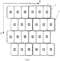
FIG. 4 is a schematic diagram of a pixel structure according to an embodiment of this application; -
FIG. 5 is a schematic structural diagram of a pixel group in a pixel structure according to an embodiment of this application; -
FIG. 6 andFIG. 7 are schematic structural diagrams of pixel group having different pixel aperture length-to-width ratios in a pixel structure according to an embodiment of this application; -
FIG. 8 is a schematic diagram of display of a pixel structure according to an embodiment of this application; and -
FIG. 9a andFIG. 9b are schematic diagrams of another pixel structure according to an embodiment of this application. - This application is described in further detail by referring to the accompanying drawings. In the respective accompanying drawings, same elements are represented by using similar reference signs. For clearness, respective parts in the accompanying drawings are not drawn proportionally. In addition, some well-known parts are not shown in the drawings.
- This embodiment is described below with reference to
FIG. 4 to FIG. 6 , where a first direction is an X direction (also referred to as a row direction or a horizontal direction), a second direction is a Y direction (also referred to as a column direction or a vertical direction), and the first direction is perpendicular to the second direction. For brevity, the accompanying drawings merely show a part of a pixel structure. In an actual product, a quantity of pixels is not limited thereto, and the quantity of pixels may be varied correspondingly according to an actual display requirement. The first row, second row, first column, second column, and the like in this application are used for describing this application by using illustrations in the drawings as reference standards, and do not refer to rows and columns in an actual product. - It should be noted that in this embodiment, the first direction and the second direction do not need to be perpendicular to each other. For convenience, descriptions are provided below by using a case in which the first direction and the second direction are perpendicular to each other.
- As shown in
FIG. 4 andFIG. 5 , a pixel structure provided by a first embodiment of this application includes a plurality of pixel groups, each of the pixel groups including afirst pixel 30 and asecond pixel 31 that are arranged adjacent in a first direction and are disposed in a staggered manner in a second direction, and each of thefirst pixel 30 and thesecond pixel 31 comprising sub-pixels of three different colors. A central line of the first sub-pixel (the sub-pixel located at an uppermost position) in thesecond pixel 31 extending along the first direction overlaps a borderline between the first sub-pixel and the second sub-pixel (the sub-pixel located at a middle position) in thefirst pixel 30. - Referring to
FIG. 9a andFIG. 9b , in another embodiment, a central line of the first sub-pixel in thefirst pixel 30 extending along the first direction overlaps a borderline between the first sub-pixel and the second sub-pixel in thesecond pixel 31. - The
first pixel 30 includes afirst sub-pixel 301, asecond sub-pixel 303, and athird sub-pixel 305 that are sequentially arranged along the second direction. Thesecond pixel 31 includes athird sub-pixel 311, afirst sub-pixel 313, and asecond sub-pixel 315 that are sequentially arranged along the second direction. - It should be noted that in this embodiment, arrangement structures of sub-pixels in the
first pixel 30 and thesecond pixel 31 are not limited to the configurations inFIG. 4 to FIG. 8 . A sub-pixel arrangement may include various permutations and combinations. For example,FIG. 9a andFIG. 9b show a configuration different from a configuration ofFIG. 4 . For convenience in description, sub-pixel arrangement structures ofFIG. 4 to FIG. 8 are used for description below. - In this embodiment, a shape of each of the sub-pixels may be a rectangle or an oblong. No limitation is imposed in this embodiment.
- In this embodiment, the first sub-pixel, the second sub-pixel, and the third sub-pixel in each of the
first pixel 30 and thesecond pixel 31 include a red (R) sub-pixel, a green (G) sub-pixel, and a blue (B) sub-pixel. That is, in the embodiment of this application, the first sub-pixel is one of the red (R) sub-pixel, the green (G) sub-pixel, and the blue (B) sub-pixel; the second sub-pixel is one of the red (R) sub-pixel, the green (G) sub-pixel, and the blue (B) sub-pixel; the third sub-pixel is one of the red (R) sub-pixel, the green (G) sub-pixel, and the blue (B) sub-pixel. Colors of the first sub-pixel, the second sub-pixel, and the third sub-pixel are different from one another. - Using
FIG. 5 as an example, in thefirst pixel 30, thefirst sub-pixel 301 is the red (R) sub-pixel, thesecond sub-pixel 303 is the green (G) sub-pixel, and thethird sub-pixel 305 is the blue (B) sub-pixel. Therefore, thefirst sub-pixel 301 includes a red (R) light-emittingregion 302 and a red (R) non-light-emitting region (not numbered in the figure), and includes an organic emission layer for emitting red light. Thesecond sub-pixel 303 includes a green (G) light-emittingregion 304 and a green (G) non-light-emitting region (not numbered in the figure), and includes an organic emission layer for emitting green light. Thethird sub-pixel 305 includes a blue (B) light-emittingregion 306 and a blue (B) non-light-emitting region (not numbered in the figure), and includes an organic emission layer for emitting blue light. In thesecond pixel 31, thefirst sub-pixel 313 is the red (R) sub-pixel, thesecond sub-pixel 315 is the green (G) sub-pixel, and thethird sub-pixel 311 is the blue (B) sub-pixel. Therefore, thefirst sub-pixel 313 includes a red (R) light-emittingregion 314 and a red (R) non-light-emitting region (not numbered in the figure), and includes an organic emitting layer for emitting red light. Thesecond sub-pixel 315 includes a green (G) light-emittingregion 316 and a green (G) non-light-emitting region (not numbered in the figure), and includes an organic emitting layer for emitting green light. Thethird sub-pixel 311 includes a blue (B) light-emittingregion 312 and a blue (B) non-light-emitting region (not numbered in the figure), and includes an organic emitting layer for emitting blue light. - A central line (shown by A in
FIG. 4 andFIG. 5 ) of thethird sub-pixel 311 in thesecond pixel 31 extending along the first direction overlaps a borderline between thefirst sub-pixel 301 and thesecond sub-pixel 303 in thefirst pixel 30. - It should be noted that because in the
first pixel 30, thefirst sub-pixel 301 and thesecond sub-pixel 303 share one side, thus, the shared side is the borderline between thefirst sub-pixel 301 and thesecond sub-pixel 303. However, it should be understood that the "border" or "borderline" described herein does not define a physical "border" or "borderline", but may refer to a virtual "border" or "borderline" between two sub-pixels in a pixel. - A distance between two sub-pixels of a same color that respectively of the
first pixel 30 and thesecond pixel 31 in the first direction is equal to that in the second direction. That is, a distance between two sub-pixels of a same color in a pixel group in the first direction is equal to that in the second direction. - Using
FIG. 6 as an example, a distance between an R sub-pixel of a first column and an R sub-pixel in a second column is x in a row direction and is y in a column direction, where x is equal to y. A distance between a G sub-pixel in the first column and a G sub-pixel in the second column is x in the row direction and is y in the column direction, where x is equal to y. A configuration of a B sub-pixel is similar to the above (not shown in the figure), and details are not described herein again. By using such a pixel arrangement, the pixels can be arranged more compactly, a spacing between pixels is reduced, and thus a PPI is increased. - In this embodiment, each of the pixels includes RGB three-color sub-pixels, and can achieve a full color display in a real sense. On the other hand, the pixel may be applied to a display panel with a resolution that is the same in the first direction and in the second direction or a display panel with a resolution that is different in the first direction and in the second direction. In a manner of sharing a sub-pixel by adjacent pixels, a pixel may present a display effect of two pixels, thereby further improving a virtual display resolution of a screen. Using the original resolution n as an example, by sharing in the first direction, the resolution of the pixel arrangement can be doubled to 2n. For a sharing manner, refer to dashed-line triangles in
FIG. 4 . For example, inFIG. 4 , an R sub-pixel and a G sub-pixel in a third column are shared by B sub-pixels that are adjacent to the R sub-pixel and the G sub-pixel, in a second column and a fourth column. A B sub-pixel of the third column is shared by R sub-pixels and G sub-pixels that are adjacent to the B sub-pixel, in the second column and the fourth column. - In an embodiment, value ranges of respective aperture length-to-width ratios of two sub-pixels of a same color respectively of the
first pixel 30 and thesecond pixel 31 are 1 to 1. 5. - Please refer to
FIG. 6 andFIG. 7 , an aperture length-to-width ratio of an R sub-pixel is d:z, where a value range of d:z is 1 to 1.5. Configurations of a G sub-pixel and a B sub-pixel are similar to the R sub-pixel. Details are not described herein again. When an aperture length-to-width ratio of a sub-pixel is 1.5, a design margin that can be satisfied is relatively large. A bridge (as shown by b inFIG. 6 and b1 inFIG. 7 ) between sub-pixels of a same color may alternatively be adjusted by adjusting a length-to-width ratio. An increase of a value of the bridge can improve a mechanical stability, reduce difficulties in manufacturing process and evaporation process of a fine metal mask, and thus a manufacturing yield can be increased. UsingFIG. 6 andFIG. 7 as examples, a bridge value b1 inFIG. 7 is greater than a bridge value b inFIG. 6 . Therefore, compared withFIG. 6 ,FIG. 7 has a higher mechanical stability, less difficulties in manufacturing process and evaporation process of a fine metal mask, and a higher manufacturing yield. - In an embodiment, in the second direction, a distance between centers of two adjacent sub-pixels is the same. The embodiment can enable the pixels to be arranged more compactly, reduce a spacing between pixels, and thus a PPI is increased.
- In an embodiment, shapes and areas of two sub-pixels of a same color respectively of the
first pixel 30 and thesecond pixel 31 are both the same. Since all sub-pixels of a same color have a same shape and a same area, manufacturing process and evaporation process difficulties for a metal mask can be further reduced. Further, shapes and areas of all sub-pixels in the pixel group may also be maintained the same. - Because the B sub-pixel has the lowest light-emitting efficiency, in the pixel group of another embodiment, an area of the red sub-pixel may be the same as an area of the green sub-pixel, and an area of the blue sub-pixel may be larger than an area of the red sub-pixel.
- A second embodiment of the present application provides an OLED display panel. The OLED display panel includes the pixel structure according to the first embodiment.
- The first embodiment may be referred to for the pixel structure. Details are not described herein again.
- To further describe this embodiment, a display solution of a pixel structure in an OLED display panel is described with reference to
FIG. 8 :
As shown inFIG. 8 , in a row direction, a length-to-width ratio of a real pixel may be 2:1. The sub-pixels of each column correspondingly display a column of pixels. Two display driving methods may be used as follows: - A first display driving method is not displaying parts of RGB sub-pixels of a corresponding image located in a dashed-line box.
- A second display driving method is displaying parts of RGB sub-pixels of a corresponding image located in a dashed-line box at a small proportion (for example, 30%) of brightness and displaying parts of RGB sub-pixels of a corresponding image not located in the dashed-line box at a large proportion (for example, 70%) of brightness. In this way, not only a brightness difference between horizontally adjacent columns can be ensured, but also display of a single point is not excessively distorted. Certainly, the brightness display proportions may be half and half (that is, the parts of the sub-pixels located in the dashed-line box are displayed at 50% of the brightness, and the parts of the sub-pixels not located in the dashed-line box are displayed at 50% of the brightness). In this way, adjacent two columns have the same brightness, thereby display details are blurred. This method is applicable to a high-PPI display.
- The embodiments according to this application are described above. All details of the embodiments are not described specifically, and this application is not limited to merely the specific embodiments either. Obviously, according to the descriptions above, many modifications and changes may be made. The embodiments that are selected and specifically described in this description are used for better explaining the principle and actual application of this application, so as to enable of a person skilled in the art to favorably use this application and modifications based on this application. This application is only limited by the claims and all scopes and equivalents of the claims.
Claims (11)
- A pixel structure comprising a plurality of pixel groups, each of the pixel groups comprising a first pixel and a second pixel adjacent in a first direction and disposed in a staggered manner in a second direction perpendicular to the first direction,
each of the first pixel and the second pixel comprising sub-pixels of three different colors arranged along the second direction; a distance between two sub-pixels of a same color respectively of the first pixel and the second pixel in the first direction is equal to that in the second direction. - The pixel structure according to claim 1, wherein a central line of a first sub-pixel in the second pixel extending along the first direction overlaps with a borderline between a first sub-pixel and a second sub-pixel in the first pixel; or
a central line of a first sub-pixel in the first pixel extending along the first direction overlaps a borderline between a first sub-pixel and a second sub-pixel in the second pixel. - The pixel structure according to claim 1, wherein the first pixel comprises a first sub-pixel, a second sub-pixel, and a third sub-pixel sequentially arranged along the second direction; and
the second pixel comprises a third sub-pixel, a first sub-pixel, and a second sub-pixel sequentially arranged along the second direction. - The pixel structure according to claim 1, wherein a length-to-width ratio of an aperture of each of the sub-pixels ranges from 1 to 1.5.
- The pixel structure according to claim 1, wherein in the second direction, distances between centers of adjacent two sub-pixels are same.
- The pixel structure according to claim 1, wherein a shape and an area of the sub-pixels of a same color in the first pixel is same to that in the second pixel, respectively.
- The pixel structure according to any one of claims 1 to 6, wherein the sub-pixels comprise a red sub-pixel, a green sub-pixel, and a blue sub-pixel.
- The pixel structure according to claim 7, wherein a shape and an area of the sub-pixels in the pixel group are respectively same.
- The pixel structure according to claim 7, wherein in the pixel group, an area of the red sub-pixel is same to an area of the green sub-pixel, and an area of the blue sub-pixel is larger than the area of the red sub-pixel.
- The pixel structure according to claims 1 to 9, wherein the first direction is a row direction and the second direction is a column direction; or
the first direction is a column direction and the second direction is a row direction. - An Organic Light-Emitting Diode (OLED) display panel comprising the pixel structure according to any one of claims 1 to 10.
Applications Claiming Priority (2)
| Application Number | Priority Date | Filing Date | Title |
|---|---|---|---|
| CN201721111056.XU CN207425858U (en) | 2017-08-31 | 2017-08-31 | A kind of dot structure and OLED display panel |
| PCT/CN2018/090495 WO2019041958A1 (en) | 2017-08-31 | 2018-06-08 | Pixel structure and oled display panel |
Publications (2)
| Publication Number | Publication Date |
|---|---|
| EP3678184A1 true EP3678184A1 (en) | 2020-07-08 |
| EP3678184A4 EP3678184A4 (en) | 2020-09-02 |
Family
ID=62315343
Family Applications (1)
| Application Number | Title | Priority Date | Filing Date |
|---|---|---|---|
| EP18851242.0A Pending EP3678184A4 (en) | 2017-08-31 | 2018-06-08 | PIXEL STRUCTURE AND OLED DISPLAY BOARD |
Country Status (6)
| Country | Link |
|---|---|
| US (1) | US11302750B2 (en) |
| EP (1) | EP3678184A4 (en) |
| JP (1) | JP7005657B2 (en) |
| KR (1) | KR20190131580A (en) |
| CN (1) | CN207425858U (en) |
| WO (1) | WO2019041958A1 (en) |
Families Citing this family (12)
| Publication number | Priority date | Publication date | Assignee | Title |
|---|---|---|---|---|
| CN207425858U (en) | 2017-08-31 | 2018-05-29 | 昆山国显光电有限公司 | A kind of dot structure and OLED display panel |
| CN108807475B (en) * | 2018-05-31 | 2020-09-25 | 昆山国显光电有限公司 | Pixel arrangement structure and OLED display panel |
| CN110767106B (en) | 2018-09-30 | 2020-09-08 | 云谷(固安)科技有限公司 | Display panel, display screen and display terminal |
| CN109801946B (en) * | 2019-01-30 | 2021-01-26 | 京东方科技集团股份有限公司 | Display panel and display device |
| KR102866754B1 (en) | 2019-03-04 | 2025-09-30 | 삼성디스플레이 주식회사 | Carrier, apparatus for manufacturing a display apparatus having the same and method for manufacturing a display apparatus |
| CN110085654B (en) * | 2019-05-29 | 2021-04-30 | 昆山国显光电有限公司 | Pixel structure, display panel with same and display device |
| EP3836222B1 (en) | 2019-12-10 | 2026-05-20 | Samsung Display Co Ltd | DISPLAY DEVICE |
| US11557635B2 (en) * | 2019-12-10 | 2023-01-17 | Samsung Display Co., Ltd. | Display device, mask assembly, and apparatus for manufacturing the display device |
| JP7665328B2 (en) * | 2020-12-18 | 2025-04-21 | JDI Design and Development 合同会社 | Display device |
| US12185608B2 (en) * | 2021-01-28 | 2024-12-31 | Innolux Corporation | Light emitting device |
| CN119968026A (en) * | 2023-11-07 | 2025-05-09 | 群创光电股份有限公司 | Electronic Devices |
| CN121218815A (en) * | 2024-06-25 | 2025-12-26 | 京东方科技集团股份有限公司 | Display substrate and display device |
Family Cites Families (11)
| Publication number | Priority date | Publication date | Assignee | Title |
|---|---|---|---|---|
| JP2003084125A (en) * | 2001-07-04 | 2003-03-19 | Seiko Epson Corp | Color filter manufacturing method and manufacturing apparatus, liquid crystal display device manufacturing method and manufacturing apparatus, EL light emitting layer mounting substrate manufacturing method and manufacturing apparatus, EL light emitting device manufacturing method and manufacturing apparatus, film forming method and film forming apparatus, Electro-optical device, method of manufacturing the same, and electronic apparatus |
| KR100626284B1 (en) | 2003-11-19 | 2006-09-21 | 엘지.필립스 엘시디 주식회사 | Organic electroluminescent device and manufacturing method thereof |
| US20060103940A1 (en) * | 2004-11-12 | 2006-05-18 | Wintek Corportation | Method for configuring luminous zones and circuit zones of pixels of the display |
| KR100748310B1 (en) | 2006-02-20 | 2007-08-09 | 삼성에스디아이 주식회사 | Organic light emitting display device and manufacturing method |
| JP5189276B2 (en) * | 2006-11-29 | 2013-04-24 | エルジー ディスプレイ カンパニー リミテッド | Image display device |
| TWI559524B (en) * | 2013-01-15 | 2016-11-21 | 友達光電股份有限公司 | Pixel structure of electroluminescent display panel |
| CN103123927B (en) | 2013-01-24 | 2015-05-06 | 昆山维信诺显示技术有限公司 | Pixel structure for OLED display screen and metal mask thereof |
| CN104319283B (en) * | 2014-10-27 | 2016-03-02 | 京东方科技集团股份有限公司 | A kind of organic elctroluminescent device, its driving method and display unit |
| CN104680948B (en) | 2015-03-31 | 2018-01-19 | 京东方科技集团股份有限公司 | A kind of dot structure, its driving method and display device |
| CN106486513B (en) | 2015-08-31 | 2023-09-29 | 昆山国显光电有限公司 | Pixel structure and OLED display panel |
| CN207425858U (en) | 2017-08-31 | 2018-05-29 | 昆山国显光电有限公司 | A kind of dot structure and OLED display panel |
-
2017
- 2017-08-31 CN CN201721111056.XU patent/CN207425858U/en active Active
-
2018
- 2018-06-08 JP JP2019563355A patent/JP7005657B2/en active Active
- 2018-06-08 EP EP18851242.0A patent/EP3678184A4/en active Pending
- 2018-06-08 KR KR1020197032735A patent/KR20190131580A/en not_active Ceased
- 2018-06-08 US US16/323,353 patent/US11302750B2/en active Active
- 2018-06-08 WO PCT/CN2018/090495 patent/WO2019041958A1/en not_active Ceased
Also Published As
| Publication number | Publication date |
|---|---|
| JP7005657B2 (en) | 2022-01-21 |
| US11302750B2 (en) | 2022-04-12 |
| EP3678184A4 (en) | 2020-09-02 |
| US20210359029A1 (en) | 2021-11-18 |
| CN207425858U (en) | 2018-05-29 |
| WO2019041958A1 (en) | 2019-03-07 |
| JP2020519965A (en) | 2020-07-02 |
| KR20190131580A (en) | 2019-11-26 |
Similar Documents
| Publication | Publication Date | Title |
|---|---|---|
| US11302750B2 (en) | Pixel structure and OLED display panel | |
| US11561465B2 (en) | Pixel arrangement structure, organic light emitting device, display device and mask | |
| US10950666B2 (en) | Pixel structure, OLED display screen and evaporation mask | |
| US10692940B2 (en) | Pixel structure and display panel having the same | |
| US20190096962A1 (en) | Pixel structure for organic light-emitting diodes, display panel and display device including the same | |
| US10700136B2 (en) | Pixel structure and organic light emitting display using the pixel structure | |
| CN106449710B (en) | Dot structure and OLED display panel comprising the dot structure | |
| US9343511B1 (en) | Pixel arrangement structure for organic light-emitting diode | |
| CN108010934B (en) | Pixel structure and forming method thereof, OLED display panel and evaporation mask | |
| CN106653799B (en) | Pixel structure and OLED display panel comprising same | |
| CN205845956U (en) | Pixel arrangement structure, display base plate, display device and mask plate | |
| CN206322697U (en) | Dot structure and the OLED display panel for including the dot structure | |
| US20180175121A1 (en) | Pixel arrangement structure, organic light-emitting diode device, display device and mask | |
| CN108091667B (en) | Pixel structure and OLED display panel comprising same | |
| CN109427852B (en) | Pixel structure, mask and display device | |
| CN107644888A (en) | Pixel arrangement structure, display base plate, display device, preparation method and mask plate | |
| CN104576696A (en) | Pixel structure and organic light emitting display adopting same | |
| CN110120406A (en) | A kind of luminescent device and preparation method thereof and display panel | |
| CN206134687U (en) | Dot structure, OLED display panel and coating by vaporization mask version | |
| CN210052744U (en) | Pixel arrangement structure, color film structure and display panel | |
| CN107248522A (en) | A kind of OLED display panel and display device | |
| CN110364546B (en) | Organic light emitting diode OLED pixel arrangement structure | |
| WO2018161704A1 (en) | Display device and manufacturing method therefor | |
| US10937836B2 (en) | Pixel arrangement structure and display device | |
| CN107359181A (en) | A kind of display panel and display device |
Legal Events
| Date | Code | Title | Description |
|---|---|---|---|
| STAA | Information on the status of an ep patent application or granted ep patent |
Free format text: STATUS: THE INTERNATIONAL PUBLICATION HAS BEEN MADE |
|
| PUAI | Public reference made under article 153(3) epc to a published international application that has entered the european phase |
Free format text: ORIGINAL CODE: 0009012 |
|
| STAA | Information on the status of an ep patent application or granted ep patent |
Free format text: STATUS: REQUEST FOR EXAMINATION WAS MADE |
|
| 17P | Request for examination filed |
Effective date: 20191122 |
|
| AK | Designated contracting states |
Kind code of ref document: A1 Designated state(s): AL AT BE BG CH CY CZ DE DK EE ES FI FR GB GR HR HU IE IS IT LI LT LU LV MC MK MT NL NO PL PT RO RS SE SI SK SM TR |
|
| AX | Request for extension of the european patent |
Extension state: BA ME |
|
| A4 | Supplementary search report drawn up and despatched |
Effective date: 20200805 |
|
| RIC1 | Information provided on ipc code assigned before grant |
Ipc: H01L 27/32 20060101AFI20200730BHEP Ipc: G09G 3/3208 20160101ALI20200730BHEP |
|
| DAV | Request for validation of the european patent (deleted) | ||
| DAX | Request for extension of the european patent (deleted) | ||
| STAA | Information on the status of an ep patent application or granted ep patent |
Free format text: STATUS: EXAMINATION IS IN PROGRESS |
|
| 17Q | First examination report despatched |
Effective date: 20251002 |