JP7005657B2 - Pixel structure and OLED display panel - Google Patents
Pixel structure and OLED display panel Download PDFInfo
- Publication number
- JP7005657B2 JP7005657B2 JP2019563355A JP2019563355A JP7005657B2 JP 7005657 B2 JP7005657 B2 JP 7005657B2 JP 2019563355 A JP2019563355 A JP 2019563355A JP 2019563355 A JP2019563355 A JP 2019563355A JP 7005657 B2 JP7005657 B2 JP 7005657B2
- Authority
- JP
- Japan
- Prior art keywords
- pixel
- sub
- pixels
- area
- red
- Prior art date
- Legal status (The legal status is an assumption and is not a legal conclusion. Google has not performed a legal analysis and makes no representation as to the accuracy of the status listed.)
- Active
Links
Images


Classifications
-
- G—PHYSICS
- G09—EDUCATION; CRYPTOGRAPHY; DISPLAY; ADVERTISING; SEALS
- G09G—ARRANGEMENTS OR CIRCUITS FOR CONTROL OF INDICATING DEVICES USING STATIC MEANS TO PRESENT VARIABLE INFORMATION
- G09G3/00—Control arrangements or circuits, of interest only in connection with visual indicators other than cathode-ray tubes
- G09G3/20—Control arrangements or circuits, of interest only in connection with visual indicators other than cathode-ray tubes for presentation of an assembly of a number of characters, e.g. a page, by composing the assembly by combination of individual elements arranged in a matrix no fixed position being assigned to or needed to be assigned to the individual characters or partial characters
- G09G3/22—Control arrangements or circuits, of interest only in connection with visual indicators other than cathode-ray tubes for presentation of an assembly of a number of characters, e.g. a page, by composing the assembly by combination of individual elements arranged in a matrix no fixed position being assigned to or needed to be assigned to the individual characters or partial characters using controlled light sources
- G09G3/30—Control arrangements or circuits, of interest only in connection with visual indicators other than cathode-ray tubes for presentation of an assembly of a number of characters, e.g. a page, by composing the assembly by combination of individual elements arranged in a matrix no fixed position being assigned to or needed to be assigned to the individual characters or partial characters using controlled light sources using electroluminescent panels
- G09G3/32—Control arrangements or circuits, of interest only in connection with visual indicators other than cathode-ray tubes for presentation of an assembly of a number of characters, e.g. a page, by composing the assembly by combination of individual elements arranged in a matrix no fixed position being assigned to or needed to be assigned to the individual characters or partial characters using controlled light sources using electroluminescent panels semiconductive, e.g. using light-emitting diodes [LED]
- G09G3/3208—Control arrangements or circuits, of interest only in connection with visual indicators other than cathode-ray tubes for presentation of an assembly of a number of characters, e.g. a page, by composing the assembly by combination of individual elements arranged in a matrix no fixed position being assigned to or needed to be assigned to the individual characters or partial characters using controlled light sources using electroluminescent panels semiconductive, e.g. using light-emitting diodes [LED] organic, e.g. using organic light-emitting diodes [OLED]
-
- H—ELECTRICITY
- H10—SEMICONDUCTOR DEVICES; ELECTRIC SOLID-STATE DEVICES NOT OTHERWISE PROVIDED FOR
- H10K—ORGANIC ELECTRIC SOLID-STATE DEVICES
- H10K59/00—Integrated devices, or assemblies of multiple devices, comprising at least one organic light-emitting element covered by group H10K50/00
- H10K59/30—Devices specially adapted for multicolour light emission
- H10K59/35—Devices specially adapted for multicolour light emission comprising red-green-blue [RGB] subpixels
- H10K59/353—Devices specially adapted for multicolour light emission comprising red-green-blue [RGB] subpixels characterised by the geometrical arrangement of the RGB subpixels
-
- H—ELECTRICITY
- H10—SEMICONDUCTOR DEVICES; ELECTRIC SOLID-STATE DEVICES NOT OTHERWISE PROVIDED FOR
- H10K—ORGANIC ELECTRIC SOLID-STATE DEVICES
- H10K50/00—Organic light-emitting devices
- H10K50/80—Constructional details
-
- G—PHYSICS
- G09—EDUCATION; CRYPTOGRAPHY; DISPLAY; ADVERTISING; SEALS
- G09G—ARRANGEMENTS OR CIRCUITS FOR CONTROL OF INDICATING DEVICES USING STATIC MEANS TO PRESENT VARIABLE INFORMATION
- G09G2300/00—Aspects of the constitution of display devices
- G09G2300/04—Structural and physical details of display devices
- G09G2300/0439—Pixel structures
- G09G2300/0452—Details of colour pixel setup, e.g. pixel composed of a red, a blue and two green components
-
- G—PHYSICS
- G09—EDUCATION; CRYPTOGRAPHY; DISPLAY; ADVERTISING; SEALS
- G09G—ARRANGEMENTS OR CIRCUITS FOR CONTROL OF INDICATING DEVICES USING STATIC MEANS TO PRESENT VARIABLE INFORMATION
- G09G2300/00—Aspects of the constitution of display devices
- G09G2300/04—Structural and physical details of display devices
- G09G2300/0439—Pixel structures
- G09G2300/0465—Improved aperture ratio, e.g. by size reduction of the pixel circuit, e.g. for improving the pixel density or the maximum displayable luminance or brightness
-
- G—PHYSICS
- G09—EDUCATION; CRYPTOGRAPHY; DISPLAY; ADVERTISING; SEALS
- G09G—ARRANGEMENTS OR CIRCUITS FOR CONTROL OF INDICATING DEVICES USING STATIC MEANS TO PRESENT VARIABLE INFORMATION
- G09G3/00—Control arrangements or circuits, of interest only in connection with visual indicators other than cathode-ray tubes
- G09G3/20—Control arrangements or circuits, of interest only in connection with visual indicators other than cathode-ray tubes for presentation of an assembly of a number of characters, e.g. a page, by composing the assembly by combination of individual elements arranged in a matrix no fixed position being assigned to or needed to be assigned to the individual characters or partial characters
- G09G3/2003—Display of colours
Description
本願はディスプレイテクノロジの分野に関し、具体的には画素構造及びその画素構造を有する有機発光ダイオード(OLED)表示パネルに関する。 The present application relates to the field of display technology, specifically, a pixel structure and an organic light emitting diode (OLED) display panel having the pixel structure.
有機発光ダイオード(OLED)は能動発光デバイスである。従来の液晶表示(LCD)ディスプレイとは対照的に、OLEDディスプレイテクノロジはバックライト源が必要なく自己発光特性がある。OLEDでは、比較的薄い有機素材膜層と、比較的薄いガラス基板とが用いられている。電流を流すとその有機素材膜層が発光する。従って、OLED表示パネルではかなり電気エネルギを節約でき、LCD表示スクリーンに比べて、軽量且つ薄手に製造すること、より広い温度変動域に耐えること、並びにその可視角をより大きくすることができる。OLED表示パネルは、LCD後の次世代パネルディスプレイテクノロジになるものと期待されており、現存するパネルディスプレイテクノロジのなかで最も関心を引いているテクノロジの一つである。 Organic light emitting diodes (OLEDs) are active light emitting devices. In contrast to traditional liquid crystal display (LCD) displays, OLED display technology does not require a backlight source and has self-luminous properties. In OLED, a relatively thin organic material film layer and a relatively thin glass substrate are used. When an electric current is applied, the organic material film layer emits light. Therefore, the OLED display panel can save a considerable amount of electrical energy, can be manufactured lighter and thinner than the LCD display screen, can withstand a wider temperature fluctuation range, and can have a larger viewing angle. OLED display panels are expected to become the next generation panel display technology after LCD, and are one of the most interesting panel display technologies in existence.
OLEDスクリーン本体発色方法は多数ある。現在、比較的成熟していて成功裏に大量生産されているOLED発色テクノロジはOLED蒸着テクノロジである。OLED蒸着テクノロジでは、従来のRGBストライプ配列形態が蒸着向けに採用されている。横並び配列は最良のピクチャ効果を有するものである。横並び配列では3個のサブ画素、即ち赤、緑及び青(R、G及びB)サブ画素が画素域内に存在する。各サブ画素は四辺形であり、独立な有機発光デバイスを有している。有機発光デバイスは、アレイ基板上の対応する画素位置に、蒸着膜形成を用いファインメタルマスク(FMM)を介し形成されており、通常はそのFMMがメタルマスク及び蒸着マスクと略称されている。PPI(1インチ(約2.5cm)当たり画素数(Pixel Per Inch))が高いOLED表示パネルを生産するテクノロジでは、微細で機械的に安定なFMM及び画素(サブ画素)配列が主に注目されている。 There are many methods for coloring the OLED screen body. Currently, the OLED coloring technology that is relatively mature and successfully mass-produced is OLED deposition technology. In OLED vapor deposition technology, the conventional RGB stripe array form is adopted for vapor deposition. The side-by-side arrangement has the best picture effect. In the side-by-side arrangement, there are three sub-pixels, namely red, green and blue (R, G and B) sub-pixels in the pixel area. Each subpixel is quadrilateral and has an independent organic light emitting device. The organic light emitting device is formed at a corresponding pixel position on the array substrate via a fine metal mask (FMM) by using a vapor deposition film formation, and the FMM is usually abbreviated as a metal mask and a vapor deposition mask. Fine and mechanically stable FMMs and pixel (sub-pixel) arrays are the main focus of technology for producing OLED display panels with high PPIs (Pixel Per Inch). ing.
図1は、従来技術におけるOLED表示パネルの画素配列の模式図である。図1に示すように、OLED表示パネルでは横並び画素配列が用いられている。各画素は、Rサブ画素領域101、Gサブ画素領域103及びBサブ画素領域105を有している。それらのうちRサブ画素領域101はR発光領域102及びR非発光領域(付番せず)を有している。Gサブ画素領域103はG発光領域104及びG非発光領域(付番せず)を有している。Bサブ画素領域105はB発光領域106及びB非発光領域(付番せず)を有している。図1に示したR、G及びBサブ画素領域の面積はそれぞれその発光領域の面積と等しく、それらR、G及びBサブ画素が直線をなして配列されている。具体的には、各サブ画素領域の発光領域はカソード、アノード及び電界発光層(有機放射層とも称する)を有している。その電界発光層はカソード・アノード間に所在しており、所定色の光を生成して表示を実現するよう構成されている。従来技術における表示パネルを準備する際には、通常、蒸着プロセスを3回実行することで、対応色(赤、緑又は青)の電界発光層をその対応色の画素領域の発光領域内にそれぞれ形成することが、必要となる。
FIG. 1 is a schematic diagram of a pixel arrangement of an OLED display panel in the prior art. As shown in FIG. 1, a side-by-side pixel arrangement is used in the OLED display panel. Each pixel has an R
通常、図1に示したOLED表示パネルにおける蒸着には図2に示すFMMが用いられる。このFMMは、遮蔽領域107と、幾つかの蒸着開口108とを有している。同じカラム内で隣り合う2個の蒸着開口108間の遮蔽領域はブリッジ(連結ブリッジ)と呼ばれている。蒸着中にサブ画素に対する遮蔽効果が生じることを避けるには、サブ画素・ブリッジ間を十分な距離に保つ必要がある。その結果として、サブ画素の垂直長が縮まり、各サブ画素の開口比が影響を受ける。従来のRGB画素横並び配列では200~300PPIにしか到達できず、この形態で高分解能表示効果を達成するのは難しい。OLED表示パネルの分解能に関するユーザの要請が高まるなか、こうしたRGB画素横並び配列では、高PPI製品設計条件を満足させることができない。
Usually, the FMM shown in FIG. 2 is used for vapor deposition in the OLED display panel shown in FIG. The FMM has a
図3は、従来技術における他のOLED表示パネルの画素配列の模式図である。図3に示すように、各画素のGサブ画素しか専用されておらず、R及びBサブ画素はそれぞれ隣り合う画素により共有されている。例えば、画素201及び画素202がRサブ画素を共有している。こうした方法であれば表示スクリーンのPPIを高めることができるが、この配列に従いR及びBサブ画素を隣り合う画素で共有させると、全体的な表示効果に歪みが入り込みかねず、また本当の意味でフルカラー表示にならない。
FIG. 3 is a schematic diagram of the pixel arrangement of another OLED display panel in the prior art. As shown in FIG. 3, only the G sub-pixel of each pixel is dedicated, and the R and B sub-pixels are shared by adjacent pixels. For example, the
本願の主目的は、画素構造及びOLED表示パネルを提供することで、従来技術に存する諸問題を解決することにある。 A main object of the present application is to solve various problems existing in the prior art by providing a pixel structure and an OLED display panel.
上述の目的を達成すべく、本願の諸実施形態の第1態様により提供される画素構造は複数個の画素群を有し、その画素群が、それぞれ、第1方向においては隣り合いその第1方向に対し垂直な第2方向においては互い違い形態にて配置された、第1画素及び第2画素を有する。 In order to achieve the above object, the pixel structure provided by the first aspect of the embodiments of the present application has a plurality of pixel groups, and the pixel groups are adjacent to each other in the first direction. It has first and second pixels arranged in a staggered manner in the second direction perpendicular to the direction.
第1画素及び第2画素は、それぞれ、第2方向に沿い配列された相異なる三色のサブ画素を有し、第1画素及び第2画素それぞれの同色サブ画素2個間の第1方向における距離が、第2方向におけるそれに等しい。 The first pixel and the second pixel each have sub-pixels of three different colors arranged along the second direction, and in the first direction between two sub-pixels of the same color of each of the first pixel and the second pixel. The distance is equal to that in the second direction.
付随的には、第1方向沿いに延びる第2画素内第1サブ画素中心線を第1画素内第1サブ画素・第2サブ画素間境界線と重ねるか、第1方向沿いに延びる第1画素内第1サブ画素中心線を第2画素内第1サブ画素・第2サブ画素間境界線と重ねる。 Concomitantly, the first sub-pixel center line in the second pixel extending along the first direction is overlapped with the boundary line between the first sub-pixel and the second sub-pixel in the first pixel, or the first extending along the first direction. The center line of the first sub-pixel in the pixel is overlapped with the boundary line between the first sub-pixel and the second sub-pixel in the second pixel.
付随的には、第1画素を、第2方向に沿いその順で配列された第1サブ画素、第2サブ画素及び第3サブ画素を有するものとし、第2画素を、第2方向に沿いその順で配列された第3サブ画素、第1サブ画素及び第2サブ画素を有するものとする。 Concomitantly, the first pixel is assumed to have a first sub-pixel, a second sub-pixel and a third sub-pixel arranged in that order along the second direction, and the second pixel is along the second direction. It is assumed that it has a third sub-pixel, a first sub-pixel, and a second sub-pixel arranged in that order.
付随的には、各サブ画素の開口の長さ対幅比を1~1.5の範囲内とする。 Concomitantly, the length-to-width ratio of the opening of each sub-pixel is set in the range of 1 to 1.5.
付随的には、隣り合う2個のサブ画素の第2方向における中心間距離を同一にする。 Concomitantly, the distance between the centers of two adjacent sub-pixels in the second direction is the same.
付随的には、第1画素内同色サブ画素の形状及び面積を第2画素内のそれとそれぞれ同一にする。 Concomitantly, the shape and area of the sub-pixels of the same color in the first pixel are made the same as those in the second pixel.
付随的には、サブ画素のなかに赤サブ画素、緑サブ画素及び青サブ画素を含める。 Concomitantly, the red sub-pixel, the green sub-pixel, and the blue sub-pixel are included in the sub-pixel.
付随的には、画素群内のサブ画素の形状及び面積それぞれを同一にする。 Concomitantly, the shape and area of the sub-pixels in the pixel group are made the same.
付随的には、画素群内で、赤サブ画素の面積を緑サブ画素の面積と同一にし、青サブ画素の面積を赤サブ画素の面積より大きくする。 Concomitantly, in the pixel group, the area of the red sub-pixel is made the same as the area of the green sub-pixel, and the area of the blue sub-pixel is made larger than the area of the red sub-pixel.
付随的には、第1方向をロー方向、第2方向をカラム方向とするか、第1方向をカラム方向、第2方向をロー方向とする。 Concomitantly, the first direction is the low direction and the second direction is the column direction, or the first direction is the column direction and the second direction is the low direction.
加えて、上掲の目的を発生すべく、本願の諸実施形態の第2態様により提供されるOLED表示パネルは、第1態様に係るいずれかの画素構造を有する。 In addition, the OLED display panel provided by the second aspect of the embodiments of the present application in order to generate the above object has any of the pixel structures according to the first aspect.
本願の諸実施形態により提供される画素構造及びOLED表示パネルでは、第1画素及び第2画素が第1方向に沿い隣り合わせに配置されていてそれぞれ相異なる三色のサブ画素を有すること、サブ画素が第2方向に沿い順次配列されること、第1方向に沿い延びる第2画素内第3サブ画素中心線が第1画素内第1サブ画素・第2サブ画素間境界線と重なること、第1画素及び第2画素それぞれの同色サブ画素2個間の第1方向における距離が第2方向におけるそれに等しいこと、という諸特徴により、本当の意味でフルカラー表示を達成することができ、且つコンパクトに配列して画素間スペースを減らし高いPPIを達成することができる。隣り合うサブ画素を共有することで、1個の画素により画素2個分の表示効果を提供することができるため、スクリーンの表示分解能と製造歩留まりとを更に改善すること、並びに蒸着マスク製造プロセス及び蒸着プロセスにおける難度を下げることができる。 In the pixel structure and the OLED display panel provided by the embodiments of the present application, the first pixel and the second pixel are arranged side by side along the first direction and have sub-pixels of three different colors. Are sequentially arranged along the second direction, the third sub-pixel center line in the second pixel extending along the first direction overlaps with the boundary line between the first sub-pixel and the second sub-pixel in the first pixel. Full-color display can be achieved in the true sense and compact due to the various features that the distance in the first direction between two sub-pixels of the same color of each of the first pixel and the second pixel is equal to that in the second direction. High PPI can be achieved by arranging and reducing the space between pixels. By sharing adjacent sub-pixels, one pixel can provide a display effect equivalent to two pixels, so that the display resolution and manufacturing yield of the screen can be further improved, and the vapor deposition mask manufacturing process and The difficulty in the vapor deposition process can be reduced.
添付図面を参照し本願をより詳細に記述する。個々の添付図面では、同じ要素が同様の参照符号を用い表されている。明瞭性のため、添付図面中の個々の部分は等比的に描かれていない。加えて、幾つかの周知部分が図面には示されていない。 The present application will be described in more detail with reference to the accompanying drawings. In the individual accompanying drawings, the same elements are represented using similar reference numerals. For clarity, the individual parts in the accompanying drawings are not drawn geometrically. In addition, some well-known parts are not shown in the drawings.
[第1実施形態]
以下、図4~図6を参照して本実施形態について記述するところ、第1方向をX方向(ロー方向又は水平方向とも称する)、第2方向をY方向(カラム方向又は垂直方向とも称する)とし、第1方向が第2方向に対し垂直であるとする。簡潔性のため、添付図面には画素構造の一部分のみを示してある。実製品では画素の量がこのようには限定されず、画素の量は実表示条件に従い相応に変わりうる。本願中の第1ロー、第2ロー、第1カラム、第2カラム等は、図面中の描写を参照標準として用いて本願を記述するために用いられており、実製品におけるロー及びカラムを指すものではない。
[First Embodiment]
Hereinafter, when the present embodiment is described with reference to FIGS. 4 to 6, the first direction is the X direction (also referred to as the low direction or the horizontal direction), and the second direction is the Y direction (also referred to as the column direction or the vertical direction). It is assumed that the first direction is perpendicular to the second direction. For brevity, the accompanying drawings show only a portion of the pixel structure. In the actual product, the amount of pixels is not limited in this way, and the amount of pixels may change accordingly according to the actual display conditions. The first row, second row, first column, second column, etc. in the present application are used to describe the present application using the description in the drawings as a reference standard, and refer to the rows and columns in the actual product. It's not a thing.
注記すべきことに、本実施形態では、第1方向及び第2方向を互いに垂直にする必要がない。便宜上、第1方向及び第2方向が互いに垂直であるケースを用いることで、以下、記述が提供されている。 It should be noted that in this embodiment, it is not necessary for the first direction and the second direction to be perpendicular to each other. For convenience, the description is provided below by using the case where the first and second directions are perpendicular to each other.
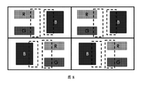
図4及び図5に示すように、本願の第1実施形態により提供される画素構造は複数個の画素群を有しており、その画素群それぞれが、第1方向においては隣り合わせに配列され第2方向においては互い違い形態にて配置された第1画素30及び第2画素31を有しており、その第1画素30及び第2画素31それぞれが、相異なる三色のサブ画素を備えている。第2画素31内第1サブ画素(最上位置に所在するサブ画素)の第1方向沿い延伸中心線が、第1画素30内第1サブ画素・第2サブ画素(中庸位置に所在するサブ画素)間境界線と重なっている。
As shown in FIGS. 4 and 5, the pixel structure provided by the first embodiment of the present application has a plurality of pixel groups, and the pixel groups are arranged side by side in the first direction. In the two directions, the
図9a及び図9bに示すように、他の実施形態では、第1画素内第1サブ画素30の第1方向沿い延伸中心線が、第2画素31内第1サブ画素・第2サブ画素間境界線と重なっている。
As shown in FIGS. 9a and 9b, in another embodiment, the extension center line of the
第1画素30は第1サブ画素301、第2サブ画素303及び第3サブ画素305を有しており、第2方向に沿いそれらがその順で配列されている。第2画素31は第3サブ画素311、第1サブ画素313及び第2サブ画素315を有しており、第2方向に沿いそれらがその順で配列されている。
The
注記すべきことに、本実施形態では、第1画素30及び第2画素31内サブ画素の配列構造が図4~図8中の構成に限定されない。サブ画素配列には様々な順列及び組合せが含まれうる。例えば、図9a及び図9bには、図4の構成とは異なる構成が示されている。記述の便宜上、以下の記述では図4~図8のサブ画素配列構造が用いられている。
It should be noted that in the present embodiment, the arrangement structure of the sub-pixels in the
本実施形態では、各サブ画素の形状を長方形や卵形にすることができる。本実施形態では何ら制限が課されていない。 In this embodiment, the shape of each sub-pixel can be rectangular or oval. No restrictions are imposed in this embodiment.
本実施形態では、第1画素30及び第2画素31それぞれのなかの第1サブ画素、第2サブ画素及び第3サブ画素に、赤(R)サブ画素、緑(G)サブ画素及び青(B)サブ画素が含まれている。即ち、本願の本実施形態では、第1サブ画素が赤(R)サブ画素、緑(G)サブ画素及び青(B)サブ画素のうち一つ、第2サブ画素が赤(R)サブ画素、緑(G)サブ画素及び青(B)サブ画素のうち一つ、第3サブ画素が赤(R)サブ画素、緑(G)サブ画素及び青(B)サブ画素のうち一つとされている。第1サブ画素、第2サブ画素及び第3サブ画素の色は互いに異なっている。
In the present embodiment, the first sub-pixel, the second sub-pixel, and the third sub-pixel in the
一例として図5を用いると、第1画素30では、第1サブ画素301が赤(R)サブ画素、第2サブ画素303が緑(G)サブ画素、第3サブ画素305が青(B)サブ画素となっている。従って、第1サブ画素301は赤(R)発光領域302及び赤(R)非発光領域(図中で付番せず)を有しており、また赤色光を放射する有機放射層を有している。第2サブ画素303は緑(G)発光領域304及び緑(G)非発光領域(図中で付番せず)を有しており、また緑色光を放射する有機放射層を有している。第3サブ画素305は青(B)発光領域306及び青(B)非発光領域(図中で付番せず)を有しており、また青色光を放射する有機放射層を有している。第2画素31では、第1サブ画素313が赤(R)サブ画素、第2サブ画素315が緑(G)サブ画素、第3サブ画素311が青(B)サブ画素となっている。従って、第1サブ画素313は赤(R)発光領域314及び赤(R)非発光領域(図中で付番せず)を有しており、また赤色光を放射する有機放射層を有している。第2サブ画素315は緑(G)発光領域316及び緑(G)非発光領域(図中で付番せず)を有しており、また緑色光を放射する有機放射層を有している。第3サブ画素311は青(B)発光領域312及び青(B)非発光領域(図中で付番せず)を有しており、また青色光を放射する有機放射層を有している。
Using FIG. 5 as an example, in the
第2画素31内第3サブ画素311の第1方向沿い延伸中心線(図4及び図5中にAで示されているもの)は、第1画素30内第1サブ画素301・第2サブ画素303間境界線と重なっている。
The extension center line (indicated by A in FIGS. 4 and 5) of the
注記すべきことに、第1画素30では第1サブ画素301及び第2サブ画素303が一辺を共有しているため、その共有辺が第1サブ画素301・第2サブ画素303間境界線となっている。しかしながら、ご理解頂くべきことに、本願記載の「境界」又は「境界線」は物理的な「境界」又は「境界線」を定めるものではなく、画素内の2個のサブ画素間の仮想的な「境界」又は「境界線」を指すこともある。
It should be noted that in the
第1画素30及び第2画素31それぞれの同色サブ画素2個間の第1方向における距離は、第2方向におけるそれに等しい。即ち、画素群内の同色サブ画素2個間の第1方向における距離が、第2方向におけるそれに等しい。
The distance between the two same-color sub-pixels of the
一例として図6を用いると、第1カラムのRサブ画素と、第2カラム内のRサブ画素との間の距離は、ロー方向においてはx、カラム方向においてはyであり、xがyに等しくなっている。第1カラム内のGサブ画素と、第2カラム内のGサブ画素との間の距離は、ロー方向においてはx、カラム方向においてはyであり、xがyに等しくなっている。Bサブ画素の構成は上掲のものと同様であるので(図中に示さず)、ここでは詳細について再述しない。こうした画素配列を用いることで、画素をよりコンパクトに配列することができ、画素間スペースが減るので、PPIが高まることとなる。 Using FIG. 6 as an example, the distance between the R subpixel in the first column and the R subpixel in the second column is x in the low direction and y in the column direction, where x is y. Are equal. The distance between the G-sub pixel in the first column and the G-sub pixel in the second column is x in the low direction and y in the column direction, where x is equal to y. Since the configuration of the B sub-pixel is the same as that shown above (not shown in the figure), the details are not described here. By using such a pixel arrangement, the pixels can be arranged more compactly, the space between pixels is reduced, and the PPI is increased.
本実施形態では、各画素がRGB三色のサブ画素を有しており、本当の意味でフルカラー表示を達成することができる。他方で、その画素は、第1方向における分解能と第2方向における分解能とが同じである表示パネルにも、第1方向における分解能と第2方向における分解能とが異なる表示パネルにも適用しうる。隣り合う画素によりサブ画素が共有される形態では、1個の画素で画素2個分の表示効果を提供できるので、スクリーンの仮想表示分解能が更に改善されることとなる。元々の分解能nを一例として用いるなら、第1方向における共有により、画素配列の分解能を2nへと倍加することができる。共有形態に関しては、図4中の破線三角形を参照されたい。例えば、図4では、第3カラム内Rサブ画素及びGサブ画素が、第2カラム内及び第4カラム内にありそれらRサブ画素及びGサブ画素と隣り合うBサブ画素によって、共有されている。第3カラムのBサブ画素が、第2カラム内及び第4カラム内にありそのBサブ画素と隣り合うRサブ画素及びGサブ画素によって、共有されている。 In the present embodiment, each pixel has RGB three-color sub-pixels, and full-color display can be achieved in the true sense. On the other hand, the pixel can be applied to a display panel in which the resolution in the first direction and the resolution in the second direction are the same, or a display panel in which the resolution in the first direction and the resolution in the second direction are different. In a form in which sub-pixels are shared by adjacent pixels, one pixel can provide a display effect equivalent to two pixels, so that the virtual display resolution of the screen is further improved. If the original resolution n is used as an example, the resolution of the pixel array can be doubled to 2n by sharing in the first direction. See the dashed triangle in FIG. 4 for the shared form. For example, in FIG. 4, the R-sub pixel and the G-sub pixel in the third column are shared by the B-sub pixel in the second column and the fourth column and adjacent to the R-sub pixel and the G-sub pixel. .. The B sub-pixel of the third column is shared by the R-sub pixel and the G-sub pixel in the second column and the fourth column and adjacent to the B sub pixel.
ある実施形態では、第1画素30及び第2画素31それぞれの同色サブ画素2個の個別開口長さ対幅比の値域が、1~1.5とされる。
In one embodiment, the range of the individual aperture length to width ratio of two sub-pixels of the same color of each of the
図6及び図7を参照頂ける通り、Rサブ画素の開口長さ対幅比はd:zであり、d:zの値域は1~1.5である。Gサブ画素及びBサブ画素の構成はRサブ画素と同様である。ここでは詳細について再述しない。サブ画素の開口長さ対幅比が1.5である場合、満足させうる設計マージンは比較的広くなる。或いは、長さ対幅比を調整することで、同色サブ画素間ブリッジ(図6にてb、図7にてb1により示されているもの)を調整してもよい。ブリッジ値の増大により機械的安定性を高め、ファインメタルマスクの製造プロセス及び蒸着プロセスにおける難度を下げることができ、ひいては製造歩留まりを高めることができる。図6及び図7を例として用いると、図7におけるブリッジ値b1は図6におけるブリッジ値bより大きい。従って、図6に比べ、図7の方が機械的安定性が高く、ファインメタルマスクの製造プロセス及び蒸着プロセスにおける難度が低く、且つ製造歩留まりが高い。 As can be seen in FIGS. 6 and 7, the aperture length to width ratio of the R subpixel is d: z, and the range of d: z is 1 to 1.5. The configurations of the G-sub pixel and the B-sub pixel are the same as those of the R-sub pixel. I will not restate the details here. When the aperture length to width ratio of the sub-pixels is 1.5, the design margin that can be satisfied is relatively wide. Alternatively, the bridge between sub-pixels of the same color (shown by b in FIG. 6 and b1 in FIG. 7) may be adjusted by adjusting the length-to-width ratio. By increasing the bridge value, the mechanical stability can be improved, the difficulty in the manufacturing process and the vapor deposition process of the fine metal mask can be reduced, and the manufacturing yield can be increased. Using FIGS. 6 and 7 as examples, the bridge value b1 in FIG. 7 is larger than the bridge value b in FIG. Therefore, compared to FIG. 6, FIG. 7 has higher mechanical stability, less difficulty in the fine metal mask manufacturing process and the vapor deposition process, and a higher manufacturing yield.
ある実施形態では、第2方向にて、隣り合う2個のサブ画素の中心間距離が同一とされる。この実施形態により、画素をよりコンパクトに配列し、画素間スペースを減らすことが可能になるため、PPIが高まる。 In one embodiment, the distance between the centers of two adjacent sub-pixels is the same in the second direction. According to this embodiment, the pixels can be arranged more compactly and the space between pixels can be reduced, so that the PPI is increased.
ある実施形態では、第1画素30及び第2画素31それぞれの同色サブ画素2個の形状及び面積が共に同一とされる。同色サブ画素全てが同形状且つ同面積であるので、メタルマスクに係る製造プロセス及び蒸着プロセスの難度を更に下げることができる。更に、画素群内のサブ画素全ての形状及び面積を同一に保つこともできる。
In one embodiment, the shapes and areas of the two sub-pixels of the same color of the
Bサブ画素の発光効率が最も低いので、他の実施形態の画素群では、赤サブ画素の面積が緑サブ画素の面積と同一とされること並びに青サブ画素の面積が赤サブ画素の面積より大きくされることがありうる。 Since the emission efficiency of the B sub-pixel is the lowest, in the pixel group of other embodiments, the area of the red sub-pixel is the same as the area of the green sub-pixel, and the area of the blue sub-pixel is larger than the area of the red sub-pixel. It can be made larger.
[第2実施形態]
本願の第2実施形態ではOLED表示パネルが提供される。本OLED表示パネルは第1実施形態に係る画素構造を有している。
[Second Embodiment]
A second embodiment of the present application provides an OLED display panel. This OLED display panel has a pixel structure according to the first embodiment.
第1実施形態でその画素構造を指すことができる。ここでは詳細について再述しない。 The pixel structure can be referred to in the first embodiment. I will not restate the details here.
本実施形態について更に記述するため、OLED表示パネル内画素構造の表示分解能について図8を参照し記述する。 In order to further describe this embodiment, the display resolution of the pixel structure in the OLED display panel will be described with reference to FIG.
図8に示すように、ロー方向における実画素の長さ対幅比は2:1とすることができる。各カラムのサブ画素により画素のカラムが相応に表される。次の如く二通りのディスプレイ駆動方法を用いることができる。 As shown in FIG. 8, the length-to-width ratio of the actual pixel in the low direction can be 2: 1. The sub-pixels of each column appropriately represent the column of pixels. Two display drive methods can be used as follows.
第1のディスプレイ駆動方法は、対応する画像のうち破線ボックス内に所在するRGBサブ画素の諸部分を表示させないものである。 The first display driving method does not display various parts of the RGB sub-pixels located in the broken line box in the corresponding image.
第2のディスプレイ駆動方法は、対応する画像のうち破線ボックス内に所在するRGBサブ画素の諸部分を低い輝度比率(例えば30%)で表示させ、且つ対応する画像のうち破線ボックス内に所在していないRGBサブ画素の諸部分を高い輝度比率(例えば70%)で表示させるものである。このやり方では、水平方向に隣り合うカラム間の輝度差を確保できるだけでなく、単一点の表示が過剰に歪まなくなる。確かなことに、輝度表示比率を半々にする(即ち、破線ボックス内に所在するサブ画素の諸部分を50%の輝度で表示させ且つ破線ボックスに所在していないサブ画素の諸部分を50%の輝度で表示させる)のでもよい。このやり方では、隣り合う2個のカラムが同輝度となり、表示細部がブラーする(ぶれる)。本方法は高PPIディスプレイに適用可能である。 The second display driving method displays various parts of the RGB sub-pixels located in the broken line box in the corresponding image at a low luminance ratio (for example, 30%), and is located in the broken line box in the corresponding image. Various parts of the RGB sub-pixels that are not used are displayed at a high luminance ratio (for example, 70%). In this method, not only the brightness difference between adjacent columns in the horizontal direction can be secured, but also the display of a single point is not excessively distorted. Certainly, the brightness display ratio is halved (that is, the parts of the sub-pixels located in the broken line box are displayed with 50% brightness, and the parts of the sub-pixels not located in the broken line box are displayed at 50%. It may be displayed with the brightness of). In this method, two adjacent columns have the same brightness, and the display details are blurred (blurred). This method is applicable to high PPI displays.
本願に係る諸実施形態について上述した。それら実施形態の詳細全てが具体的に記述されてはいないし、本願がそれら具体的実施形態のみに限定されるものでもない。自明な通り、上掲の記述に従い、多くの修正及び変更をなすことができる。本明細書にて選択され具体的に記述された諸実施形態は、本願の原理及び実適用をより良好に説明するために用いられており、それにより、本件技術分野に習熟した者(いわゆる当業者)が本願並びに本願に基づく修正物を好適に用いることが可能となる。本願は、特許請求の範囲と、特許請求の範囲の全技術的範囲及び均等物によってのみ、限定される。
The embodiments according to the present application have been described above. Not all of the details of those embodiments are specifically described, nor is the present application limited to these specific embodiments. Obviously, many amendments and changes can be made in accordance with the above description. The embodiments selected and specifically described herein are used to better explain the principles and practical applications of the present application, thereby those skilled in the art (so-called present). It will be possible for a person skilled in the art) to preferably use the present application and the modified product based on the present application. The present application is limited only by the scope of claims and the entire technical scope and equivalents of the scope of claims.
Claims (7)
第1画素が、第2方向に沿いに配列された第1サブ画素、第2サブ画素及び第3サブ画素を備え、第2画素が、第2方向に沿いに配列された第3サブ画素、第1サブ画素及び第2サブ画素を備え、第1サブ画素、第2サブ画素及び第3サブ画素はそれぞれ赤色、緑色及び青色から選択され、
第1の方向に沿った第1画素と第2画素との間の間隙は、第1画素及び第2画素それぞれの同色サブ画素2個の中心の間の第1方向における距離が、第2方向におけるそれに等しくなるようにされており、
前記画素群内で、赤サブ画素の面積が緑サブ画素の面積と同一であり且つ青サブ画素の面積が赤サブ画素の面積より大きい画素構造。 It is a pixel structure including a plurality of pixel groups, and the first pixel and the first pixel group are arranged in a staggered manner in a second direction perpendicular to the first direction and adjacent to each other in the first direction. Equipped with 2 pixels
The first pixel comprises a first sub-pixel, a second sub-pixel and a third sub-pixel arranged along a second direction, and a second pixel is a third sub-pixel arranged along a second direction. The first sub-pixel and the second sub-pixel are provided, and the first sub-pixel, the second sub-pixel and the third sub-pixel are selected from red, green and blue, respectively.
The gap between the first pixel and the second pixel along the first direction is such that the distance in the first direction between the centers of the two same-color subpixels of the first pixel and the second pixel is the second direction. Is made to be equal to that in
Within the pixel group, a pixel structure in which the area of the red sub-pixel is the same as the area of the green sub-pixel and the area of the blue sub-pixel is larger than the area of the red sub-pixel.
第1方向沿いに延びる第1画素内第1サブ画素中心線が第2画素内第1サブ画素・第2サブ画素間境界線と重なっている、
請求項1記載の画素構造。 Whether the center line of the first sub-pixel in the second pixel extending along the first direction overlaps with the boundary line between the first sub-pixel and the second sub-pixel in the first pixel.
The center line of the first sub-pixel in the first pixel extending along the first direction overlaps with the boundary line between the first sub-pixel and the second sub-pixel in the second pixel.
The pixel structure according to claim 1.
第1方向がロー方向であり第2方向がカラム方向であるか、
第1方向がカラム方向であり第2方向がロー方向である、
請求項1乃至5のうちいずれか一項記載の画素構造。 Sub-pixels include red sub-pixels, green sub-pixels and blue sub-pixels.
Whether the first direction is the low direction and the second direction is the column direction
The first direction is the column direction and the second direction is the low direction.
The pixel structure according to any one of claims 1 to 5 .
Applications Claiming Priority (3)
| Application Number | Priority Date | Filing Date | Title |
|---|---|---|---|
| CN201721111056.XU CN207425858U (en) | 2017-08-31 | 2017-08-31 | A kind of dot structure and OLED display panel |
| CN201721111056.X | 2017-08-31 | ||
| PCT/CN2018/090495 WO2019041958A1 (en) | 2017-08-31 | 2018-06-08 | Pixel structure and oled display panel |
Publications (2)
| Publication Number | Publication Date |
|---|---|
| JP2020519965A JP2020519965A (en) | 2020-07-02 |
| JP7005657B2 true JP7005657B2 (en) | 2022-01-21 |
Family
ID=62315343
Family Applications (1)
| Application Number | Title | Priority Date | Filing Date |
|---|---|---|---|
| JP2019563355A Active JP7005657B2 (en) | 2017-08-31 | 2018-06-08 | Pixel structure and OLED display panel |
Country Status (6)
| Country | Link |
|---|---|
| US (1) | US11302750B2 (en) |
| EP (1) | EP3678184A4 (en) |
| JP (1) | JP7005657B2 (en) |
| KR (1) | KR20190131580A (en) |
| CN (1) | CN207425858U (en) |
| WO (1) | WO2019041958A1 (en) |
Families Citing this family (7)
| Publication number | Priority date | Publication date | Assignee | Title |
|---|---|---|---|---|
| CN207425858U (en) | 2017-08-31 | 2018-05-29 | 昆山国显光电有限公司 | A kind of dot structure and OLED display panel |
| CN108807475B (en) * | 2018-05-31 | 2020-09-25 | 昆山国显光电有限公司 | Pixel arrangement structure and OLED display panel |
| CN110767106B (en) * | 2018-09-30 | 2020-09-08 | 云谷(固安)科技有限公司 | Display panel, display screen and display terminal |
| KR20200106589A (en) | 2019-03-04 | 2020-09-15 | 삼성디스플레이 주식회사 | Carrier, apparatus for manufacturing a display apparatus having the same and method for manufacturing a display apparatus |
| CN110085654B (en) * | 2019-05-29 | 2021-04-30 | 昆山国显光电有限公司 | Pixel structure, display panel with same and display device |
| US11557635B2 (en) * | 2019-12-10 | 2023-01-17 | Samsung Display Co., Ltd. | Display device, mask assembly, and apparatus for manufacturing the display device |
| US20220238611A1 (en) * | 2021-01-28 | 2022-07-28 | Innolux Corporation | Light emitting device |
Citations (3)
| Publication number | Priority date | Publication date | Assignee | Title |
|---|---|---|---|---|
| JP2008135333A (en) | 2006-11-29 | 2008-06-12 | Kyocera Corp | Image display device |
| JP2016513334A (en) | 2013-01-24 | 2016-05-12 | クンシャン ビジオノックス ディスプレイ カンパニー リミテッド | Pixel structure used in OLED display device and metal mask thereof |
| US20160293084A1 (en) | 2015-03-31 | 2016-10-06 | Boe Technology Group Co., Ltd. | Pixel structure, method for driving pixel structure and display apparatus |
Family Cites Families (8)
| Publication number | Priority date | Publication date | Assignee | Title |
|---|---|---|---|---|
| JP2003084125A (en) | 2001-07-04 | 2003-03-19 | Seiko Epson Corp | Method and device for manufacturing color filter, method and device for manufacturing liquid crystal display device, method and device for manufacturing substrate for installing el (electroluminescence) light emitting layer, method and device for manufacturing el light emitting device, method and device for film forming |
| KR100626284B1 (en) | 2003-11-19 | 2006-09-21 | 엘지.필립스 엘시디 주식회사 | Organic Electro Luminescence Device And Fabricating Method Thereof |
| US20060103940A1 (en) * | 2004-11-12 | 2006-05-18 | Wintek Corportation | Method for configuring luminous zones and circuit zones of pixels of the display |
| KR100748310B1 (en) | 2006-02-20 | 2007-08-09 | 삼성에스디아이 주식회사 | Organic light emitting display and the making method the same |
| TWI559524B (en) * | 2013-01-15 | 2016-11-21 | 友達光電股份有限公司 | Pixel structure of electroluminescent display panel |
| CN104319283B (en) | 2014-10-27 | 2016-03-02 | 京东方科技集团股份有限公司 | A kind of organic elctroluminescent device, its driving method and display unit |
| CN106486513B (en) * | 2015-08-31 | 2023-09-29 | 昆山国显光电有限公司 | Pixel structure and OLED display panel |
| CN207425858U (en) | 2017-08-31 | 2018-05-29 | 昆山国显光电有限公司 | A kind of dot structure and OLED display panel |
-
2017
- 2017-08-31 CN CN201721111056.XU patent/CN207425858U/en active Active
-
2018
- 2018-06-08 KR KR1020197032735A patent/KR20190131580A/en not_active IP Right Cessation
- 2018-06-08 US US16/323,353 patent/US11302750B2/en active Active
- 2018-06-08 WO PCT/CN2018/090495 patent/WO2019041958A1/en unknown
- 2018-06-08 EP EP18851242.0A patent/EP3678184A4/en active Pending
- 2018-06-08 JP JP2019563355A patent/JP7005657B2/en active Active
Patent Citations (3)
| Publication number | Priority date | Publication date | Assignee | Title |
|---|---|---|---|---|
| JP2008135333A (en) | 2006-11-29 | 2008-06-12 | Kyocera Corp | Image display device |
| JP2016513334A (en) | 2013-01-24 | 2016-05-12 | クンシャン ビジオノックス ディスプレイ カンパニー リミテッド | Pixel structure used in OLED display device and metal mask thereof |
| US20160293084A1 (en) | 2015-03-31 | 2016-10-06 | Boe Technology Group Co., Ltd. | Pixel structure, method for driving pixel structure and display apparatus |
Also Published As
| Publication number | Publication date |
|---|---|
| US11302750B2 (en) | 2022-04-12 |
| EP3678184A1 (en) | 2020-07-08 |
| EP3678184A4 (en) | 2020-09-02 |
| JP2020519965A (en) | 2020-07-02 |
| WO2019041958A1 (en) | 2019-03-07 |
| KR20190131580A (en) | 2019-11-26 |
| CN207425858U (en) | 2018-05-29 |
| US20210359029A1 (en) | 2021-11-18 |
Similar Documents
| Publication | Publication Date | Title |
|---|---|---|
| JP7005657B2 (en) | Pixel structure and OLED display panel | |
| US10950666B2 (en) | Pixel structure, OLED display screen and evaporation mask | |
| US10692940B2 (en) | Pixel structure and display panel having the same | |
| KR102035851B1 (en) | Pixel Structure and Organic Light Emitting Diode (OLED) Display Panel | |
| EP3346497B1 (en) | Pixel structure and oled display panel | |
| US10700136B2 (en) | Pixel structure and organic light emitting display using the pixel structure | |
| KR101700558B1 (en) | Organic light emitting display device | |
| US20190096962A1 (en) | Pixel structure for organic light-emitting diodes, display panel and display device including the same | |
| CN108010934B (en) | Pixel structure and forming method thereof, OLED display panel and evaporation mask | |
| US20180053811A1 (en) | Arrangement of color sub-pixels for full color oled and method of manufacturing same | |
| CN106653799B (en) | Pixel structure and OLED display panel comprising same | |
| CN206322697U (en) | Dot structure and the OLED display panel for including the dot structure | |
| WO2018196496A1 (en) | Pixel structure driving method | |
| WO2017118003A1 (en) | Oled pixel array, method of manufacturing oled pixel array, and oled display panel and display device | |
| US20180212001A1 (en) | Pixel structure, fabrication method thereof, display panel, and display apparatus | |
| CN106157877A (en) | Dot structure and display device | |
| WO2019062278A1 (en) | Pixel arrangement structure, pixel structure and manufacturing method thereof, array substrate, and display panel | |
| CN104659064A (en) | Organic light emitting diode display pixel array structure and display device | |
| JP3211280U (en) | Organic light emitting display panel | |
| CN108807475B (en) | Pixel arrangement structure and OLED display panel | |
| CN212412057U (en) | Display panel, mask assembly and display device | |
| US10937836B2 (en) | Pixel arrangement structure and display device | |
| CN110364546B (en) | Organic light emitting diode OLED pixel arrangement structure | |
| KR20170120488A (en) | Organic light emitting display device | |
| CN113097273B (en) | Display panel and display device |
Legal Events
| Date | Code | Title | Description |
|---|---|---|---|
| A521 | Request for written amendment filed |
Free format text: JAPANESE INTERMEDIATE CODE: A523 Effective date: 20191115 |
|
| A621 | Written request for application examination |
Free format text: JAPANESE INTERMEDIATE CODE: A621 Effective date: 20191115 |
|
| A977 | Report on retrieval |
Free format text: JAPANESE INTERMEDIATE CODE: A971007 Effective date: 20201215 |
|
| A131 | Notification of reasons for refusal |
Free format text: JAPANESE INTERMEDIATE CODE: A131 Effective date: 20210119 |
|
| A521 | Request for written amendment filed |
Free format text: JAPANESE INTERMEDIATE CODE: A523 Effective date: 20210406 |
|
| A02 | Decision of refusal |
Free format text: JAPANESE INTERMEDIATE CODE: A02 Effective date: 20210831 |
|
| A521 | Request for written amendment filed |
Free format text: JAPANESE INTERMEDIATE CODE: A523 Effective date: 20211104 |
|
| C60 | Trial request (containing other claim documents, opposition documents) |
Free format text: JAPANESE INTERMEDIATE CODE: C60 Effective date: 20211104 |
|
| A911 | Transfer to examiner for re-examination before appeal (zenchi) |
Free format text: JAPANESE INTERMEDIATE CODE: A911 Effective date: 20211115 |
|
| C21 | Notice of transfer of a case for reconsideration by examiners before appeal proceedings |
Free format text: JAPANESE INTERMEDIATE CODE: C21 Effective date: 20211116 |
|
| TRDD | Decision of grant or rejection written | ||
| A01 | Written decision to grant a patent or to grant a registration (utility model) |
Free format text: JAPANESE INTERMEDIATE CODE: A01 Effective date: 20220104 |
|
| A61 | First payment of annual fees (during grant procedure) |
Free format text: JAPANESE INTERMEDIATE CODE: A61 Effective date: 20220105 |
|
| R150 | Certificate of patent or registration of utility model |
Ref document number: 7005657 Country of ref document: JP Free format text: JAPANESE INTERMEDIATE CODE: R150 |