EP3676639B1 - Détecteur multicouche à scintillateur monolithique - Google Patents
Détecteur multicouche à scintillateur monolithique Download PDFInfo
- Publication number
- EP3676639B1 EP3676639B1 EP18758583.1A EP18758583A EP3676639B1 EP 3676639 B1 EP3676639 B1 EP 3676639B1 EP 18758583 A EP18758583 A EP 18758583A EP 3676639 B1 EP3676639 B1 EP 3676639B1
- Authority
- EP
- European Patent Office
- Prior art keywords
- scintillator
- monolithic
- ray radiation
- array
- optically reflective
- Prior art date
- Legal status (The legal status is an assumption and is not a legal conclusion. Google has not performed a legal analysis and makes no representation as to the accuracy of the status listed.)
- Active
Links
- 230000004888 barrier function Effects 0.000 claims description 81
- 239000000463 material Substances 0.000 claims description 68
- 230000005855 radiation Effects 0.000 claims description 64
- 239000013078 crystal Substances 0.000 claims description 19
- 238000002591 computed tomography Methods 0.000 claims description 18
- 238000003491 array Methods 0.000 claims description 13
- 238000000034 method Methods 0.000 claims description 11
- 229910019901 yttrium aluminum garnet Inorganic materials 0.000 claims description 6
- 229910019655 synthetic inorganic crystalline material Inorganic materials 0.000 claims description 5
- PFNQVRZLDWYSCW-UHFFFAOYSA-N (fluoren-9-ylideneamino) n-naphthalen-1-ylcarbamate Chemical compound C12=CC=CC=C2C2=CC=CC=C2C1=NOC(=O)NC1=CC=CC2=CC=CC=C12 PFNQVRZLDWYSCW-UHFFFAOYSA-N 0.000 claims description 4
- BEZBEMZKLAZARX-UHFFFAOYSA-N alumane;gadolinium Chemical compound [AlH3].[Gd] BEZBEMZKLAZARX-UHFFFAOYSA-N 0.000 claims description 3
- 229910052733 gallium Inorganic materials 0.000 claims description 3
- 239000002223 garnet Substances 0.000 claims description 3
- 238000004519 manufacturing process Methods 0.000 claims description 3
- 229910052684 Cerium Inorganic materials 0.000 claims description 2
- MCVAAHQLXUXWLC-UHFFFAOYSA-N [O-2].[O-2].[S-2].[Gd+3].[Gd+3] Chemical compound [O-2].[O-2].[S-2].[Gd+3].[Gd+3] MCVAAHQLXUXWLC-UHFFFAOYSA-N 0.000 claims description 2
- JNDMLEXHDPKVFC-UHFFFAOYSA-N aluminum;oxygen(2-);yttrium(3+) Chemical compound [O-2].[O-2].[O-2].[Al+3].[Y+3] JNDMLEXHDPKVFC-UHFFFAOYSA-N 0.000 claims description 2
- 229910052793 cadmium Inorganic materials 0.000 claims description 2
- BDOSMKKIYDKNTQ-UHFFFAOYSA-N cadmium atom Chemical compound [Cd] BDOSMKKIYDKNTQ-UHFFFAOYSA-N 0.000 claims description 2
- GWXLDORMOJMVQZ-UHFFFAOYSA-N cerium Chemical compound [Ce] GWXLDORMOJMVQZ-UHFFFAOYSA-N 0.000 claims description 2
- PBYZMCDFOULPGH-UHFFFAOYSA-N tungstate Chemical compound [O-][W]([O-])(=O)=O PBYZMCDFOULPGH-UHFFFAOYSA-N 0.000 claims description 2
- 229910019990 cerium-doped yttrium aluminum garnet Inorganic materials 0.000 claims 1
- 239000010410 layer Substances 0.000 description 27
- 230000003287 optical effect Effects 0.000 description 14
- 239000000758 substrate Substances 0.000 description 10
- 239000002355 dual-layer Substances 0.000 description 9
- 230000003595 spectral effect Effects 0.000 description 8
- 239000013590 bulk material Substances 0.000 description 5
- 239000011248 coating agent Substances 0.000 description 4
- 238000000576 coating method Methods 0.000 description 4
- 230000000295 complement effect Effects 0.000 description 4
- 238000000926 separation method Methods 0.000 description 4
- 238000013170 computed tomography imaging Methods 0.000 description 3
- 238000001514 detection method Methods 0.000 description 2
- 230000000149 penetrating effect Effects 0.000 description 2
- RFVFQQWKPSOBED-PSXMRANNSA-N 1-myristoyl-2-palmitoyl-sn-glycero-3-phosphocholine Chemical group CCCCCCCCCCCCCCCC(=O)O[C@@H](COP([O-])(=O)OCC[N+](C)(C)C)COC(=O)CCCCCCCCCCCCC RFVFQQWKPSOBED-PSXMRANNSA-N 0.000 description 1
- ZCYVEMRRCGMTRW-UHFFFAOYSA-N 7553-56-2 Chemical compound [I] ZCYVEMRRCGMTRW-UHFFFAOYSA-N 0.000 description 1
- OYPRJOBELJOOCE-UHFFFAOYSA-N Calcium Chemical compound [Ca] OYPRJOBELJOOCE-UHFFFAOYSA-N 0.000 description 1
- GWEVSGVZZGPLCZ-UHFFFAOYSA-N Titan oxide Chemical compound O=[Ti]=O GWEVSGVZZGPLCZ-UHFFFAOYSA-N 0.000 description 1
- 238000010521 absorption reaction Methods 0.000 description 1
- 238000004026 adhesive bonding Methods 0.000 description 1
- 210000000988 bone and bone Anatomy 0.000 description 1
- 229910052791 calcium Inorganic materials 0.000 description 1
- 239000011575 calcium Substances 0.000 description 1
- 238000004364 calculation method Methods 0.000 description 1
- 230000008859 change Effects 0.000 description 1
- 238000000701 chemical imaging Methods 0.000 description 1
- 230000008878 coupling Effects 0.000 description 1
- 238000010168 coupling process Methods 0.000 description 1
- 238000005859 coupling reaction Methods 0.000 description 1
- 230000001419 dependent effect Effects 0.000 description 1
- 230000009977 dual effect Effects 0.000 description 1
- 230000000694 effects Effects 0.000 description 1
- 238000011156 evaluation Methods 0.000 description 1
- 230000005251 gamma ray Effects 0.000 description 1
- 238000003384 imaging method Methods 0.000 description 1
- 229910052740 iodine Inorganic materials 0.000 description 1
- 239000011630 iodine Substances 0.000 description 1
- 238000010147 laser engraving Methods 0.000 description 1
- RCVOTEPLGFCFIG-UHFFFAOYSA-N lutetium(3+);yttrium(3+);silicate Chemical compound [Y+3].[Lu+3].[O-][Si]([O-])([O-])[O-] RCVOTEPLGFCFIG-UHFFFAOYSA-N 0.000 description 1
- 238000005535 overpotential deposition Methods 0.000 description 1
- 239000003973 paint Substances 0.000 description 1
- 230000008569 process Effects 0.000 description 1
- 238000005316 response function Methods 0.000 description 1
- 210000004872 soft tissue Anatomy 0.000 description 1
- 238000003860 storage Methods 0.000 description 1
Images


Classifications
-
- G—PHYSICS
- G01—MEASURING; TESTING
- G01N—INVESTIGATING OR ANALYSING MATERIALS BY DETERMINING THEIR CHEMICAL OR PHYSICAL PROPERTIES
- G01N23/00—Investigating or analysing materials by the use of wave or particle radiation, e.g. X-rays or neutrons, not covered by groups G01N3/00 – G01N17/00, G01N21/00 or G01N22/00
- G01N23/02—Investigating or analysing materials by the use of wave or particle radiation, e.g. X-rays or neutrons, not covered by groups G01N3/00 – G01N17/00, G01N21/00 or G01N22/00 by transmitting the radiation through the material
- G01N23/04—Investigating or analysing materials by the use of wave or particle radiation, e.g. X-rays or neutrons, not covered by groups G01N3/00 – G01N17/00, G01N21/00 or G01N22/00 by transmitting the radiation through the material and forming images of the material
- G01N23/046—Investigating or analysing materials by the use of wave or particle radiation, e.g. X-rays or neutrons, not covered by groups G01N3/00 – G01N17/00, G01N21/00 or G01N22/00 by transmitting the radiation through the material and forming images of the material using tomography, e.g. computed tomography [CT]
-
- G—PHYSICS
- G01—MEASURING; TESTING
- G01T—MEASUREMENT OF NUCLEAR OR X-RADIATION
- G01T1/00—Measuring X-radiation, gamma radiation, corpuscular radiation, or cosmic radiation
- G01T1/16—Measuring radiation intensity
- G01T1/20—Measuring radiation intensity with scintillation detectors
- G01T1/202—Measuring radiation intensity with scintillation detectors the detector being a crystal
-
- G—PHYSICS
- G01—MEASURING; TESTING
- G01T—MEASUREMENT OF NUCLEAR OR X-RADIATION
- G01T1/00—Measuring X-radiation, gamma radiation, corpuscular radiation, or cosmic radiation
- G01T1/16—Measuring radiation intensity
- G01T1/20—Measuring radiation intensity with scintillation detectors
- G01T1/2018—Scintillation-photodiode combinations
- G01T1/20183—Arrangements for preventing or correcting crosstalk, e.g. optical or electrical arrangements for correcting crosstalk
-
- G—PHYSICS
- G01—MEASURING; TESTING
- G01T—MEASUREMENT OF NUCLEAR OR X-RADIATION
- G01T1/00—Measuring X-radiation, gamma radiation, corpuscular radiation, or cosmic radiation
- G01T1/16—Measuring radiation intensity
- G01T1/20—Measuring radiation intensity with scintillation detectors
- G01T1/2018—Scintillation-photodiode combinations
- G01T1/20185—Coupling means between the photodiode and the scintillator, e.g. optical couplings using adhesives with wavelength-shifting fibres
-
- G—PHYSICS
- G01—MEASURING; TESTING
- G01T—MEASUREMENT OF NUCLEAR OR X-RADIATION
- G01T1/00—Measuring X-radiation, gamma radiation, corpuscular radiation, or cosmic radiation
- G01T1/29—Measurement performed on radiation beams, e.g. position or section of the beam; Measurement of spatial distribution of radiation
- G01T1/2914—Measurement of spatial distribution of radiation
- G01T1/2985—In depth localisation, e.g. using positron emitters; Tomographic imaging (longitudinal and transverse section imaging; apparatus for radiation diagnosis sequentially in different planes, steroscopic radiation diagnosis)
-
- H—ELECTRICITY
- H01—ELECTRIC ELEMENTS
- H01L—SEMICONDUCTOR DEVICES NOT COVERED BY CLASS H10
- H01L27/00—Devices consisting of a plurality of semiconductor or other solid-state components formed in or on a common substrate
- H01L27/14—Devices consisting of a plurality of semiconductor or other solid-state components formed in or on a common substrate including semiconductor components sensitive to infrared radiation, light, electromagnetic radiation of shorter wavelength or corpuscular radiation and specially adapted either for the conversion of the energy of such radiation into electrical energy or for the control of electrical energy by such radiation
- H01L27/144—Devices controlled by radiation
- H01L27/146—Imager structures
- H01L27/14643—Photodiode arrays; MOS imagers
- H01L27/14658—X-ray, gamma-ray or corpuscular radiation imagers
- H01L27/14663—Indirect radiation imagers, e.g. using luminescent members
Definitions
- the following relates to a computed tomography (CT) detector array a computed tomography system and a method of manufacturing a computed tomography (CT) radiation detecting apparatus.
- CT computed tomography
- a spectral CT imaging system includes a single broadband source, multiple sources, and/or kVp switching to emit x-ray radiation.
- the emitted x-ray radiation traverses an examination region with an object or subjected located within.
- One configuration includes a multi-layer detector array, located across the examination region from the source that detects x-ray radiation traversing the examination region and impinging thereon.
- the multi-layer detector array includes multiple detector modules, each with multiple detector elements that extend in one or two dimensions in a direction transverse to the incident radiation.
- the X-ray radiation receiving surfaces of the detector elements are also referred to as pixels herein.
- WO2012/127403A2 describes that a method includes obtaining a photosensor substrate having two opposing major surfaces. One of the two opposing major surfaces includes at least one photosensor row of at least one photosensor element, and the obtained photosensor substrate has a thickness equal to or greater than one hundred microns.
- the method further includes optically coupling a scintillator array to the photosensor substrate.
- the scintillator array includes at least one complementary scintillator row of at least one complementary scintillator element, and the at least one complementary scintillator row is optically coupled to the at least one photosensor row and the at least one complementary scintillator element is optically coupled to the at least one photosensor element.
- the method further includes thinning the photosensor substrate optically coupled to the scintillator producing a thinned photosensor substrate that is optically coupled to the scintillator and that has a thickness on the order of less than one hundred microns.
- a radiation detector includes a two-dimensional array of upper scintillators which is disposed facing an x-ray source to convert lower energy radiation events into visible light and transmit higher energy radiation.
- a two-dimensional array of lower scintillators is disposed adjacent the upper scintillators distally from the x-ray source to convert the transmitted higher energy radiation into visible light.
- Upper and lower photodetectors are optically coupled to the respective upper and lower scintillators at an inner side of the scintillators.
- An optical element is optically coupled with the upper scintillators to collect and channel the light from the upper scintillators into corresponding upper photodetectors.
- the authors describe that in this study, to fabricate the 3D crystal block efficiently and precisely, they applied a sub-surface laser engraving (SSLE) technique to a monolithic crystal block instead of gluing segmented small crystals.
- SSLE sub-surface laser engraving
- the SSLE technique provided micro-crack walls which carve a groove into a monolithic scintillator block.
- the authors describe that they evaluated its intrinsic spatial resolution to show a proof of concept of isotropic resolution. It is described that the 3D grids of 2 mm pitch were fabricated into an 18 ⁇ 18 ⁇ 18 mm(3) monolithic lutetium yttrium orthosilicate (LYSO) crystal by the SSLE technique.
- LYSO monolithic lutetium yttrium orthosilicate
- each detector element includes two layers of cuboid shaped and/or frustrum of a square right pyramid shaped scintillators (or scintillator voxels).
- the layers are stacked one on top of another and the stack extends in a direction of the incident radiation.
- a first scintillator in a first layer receives and absorbs X-ray radiation of a first predetermined energy range and produces first light radiation indicative thereof.
- X-ray radiation greater than the first predetermined energy range traverses the first scintillator and is detected by a second scintillator in a second layer, which receives and absorbs this X-ray radiation and produces second light radiation indicative thereof.
- the light radiation is detected by corresponding photosensors, such as photodiodes, which produce electrical signals indicative of an energy of the X-ray radiation.
- Photosensors can be arranged in a vertical or horizontal configuration.
- photosensors are arranged between scintillators and occupy a portion of a surface of the detector that receives the X-ray radiation.
- the photosensors arranged as an array are generally parallel to the incident radiation.
- photosensors are placed in front of or behind the scintillators relative to the X-ray radiation.
- the photosensors arranged as an array are generally perpendicular to the incident radiation.
- the photosensors When placed in front of or between the X-ray radiation and the scintillator, it is advantageous for the photosensors to be transparent to the X-ray radiation, such that the X-ray radiation passes through the photosensors and is then absorbed by the scintillators.
- Each scintillator in each layer of each detector element is typically coated with optically reflective material (e.g., titanium dioxide (TiO 2 ), white paint, etc.) on five of six sides of the cuboid with a sixth side adjacent a corresponding photosensor.
- optically reflective material e.g., titanium dioxide (TiO 2 ), white paint, etc.
- the optically reflective material can mitigate cross talk of light between scintillator of each layer and/or voxel, improve detection efficiency, and/or direct the light to the corresponding photosensor where it is converted to an electrical signal.
- Each scintillator of each layer of each detector element has been mechanically produced (e.g., with a saw, a wire, etc.) and coated with the optically reflective material, and then the scintillators are aligned and stacked.
- the aligning and stacking process can be complex, and it can be difficult to accurately align and stack the scintillators.
- a surface of a first scintillator in a first layer should align with and match a corresponding surface of a second scintillator in a second layer of the same detector element, and the scintillators should align with the corresponding photosensors of each layer.
- inaccurate alignment and/or stacking can lead to detection inefficiencies and degraded image quality.
- appended claim 1 defines a computed tomography (CT) detector array.
- appended claim 6 defines a computed tomography system.
- appended claim 7 defines a method of manufacturing a computed tomography (CT) radiation detecting apparatus.
- the invention may take form in various components and arrangements of components, and in various steps and arrangements of steps.
- the drawings are only for purposes of illustrating the preferred embodiments and are not to be construed as limiting the invention.
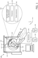
- the CT imaging system 100 includes a rotating gantry 112 supported by a stationary gantry 114.
- the CT imaging system 100 includes an X-ray radiation source 116 supported by the rotating gantry 112 and configured to emit X-ray radiation.
- the emitted X-ray radiation traverses an examination region 118.
- the X-ray radiation traversing the examination region 118 is detected by a multi (e.g., dual) -layer radiation sensitive detector array 120, which is supported by the rotating gantry 112, across from the X-ray radiation source 116.
- a subject support 119 such as a couch, supports an object or subject in the examination region 118.
- a magnified view 122 of a portion of the multi-layer detector array 120 is illustrated.
- the array 120 includes a monolithic scintillator 124.
- the monolithic scintillator 124 includes a plurality of scintillator regions (scintillator voxels), and the regions are separated by an optically reflective barrier therebetween.
- the optically reflective barrier is induced by one or more lasers, etc.
- the induced optically reflective barrier maintains the physical bulk of scintillator material as a single block while adding a reflective barrier between regions by changing the crystal structure of the scintillator material within dimensions of the optically reflective barrier.
- the scintillator material can include, but is not limited to, Gadolinium Oxysulfide (GOS, Gd 2 O 2 S), Yttrium Aluminum Garnet (YAG, Y 3 Al 5 O 12 ), Ce doped YAG (Ce-YAG, Ce Y 3 Al 5 O 12 ), Zinc Selenide (ZnSe), Cadmium Tungstate (CdWO 4 ), Gadolinium Aluminum Gallium Garnet (GAGG Gd 3 Al 2 GA 3 O 12 ), Cerium doped GAGG (Ce Gd 3 Al 2 GA 3 O 12 ), etc.
- the monolithic scintillator 124 mitigates the complexity associated with accurately aligning scintillator voxels, e.g., in a configuration in which layers of scintillator material in each detector element are physically separate and mechanically coupled together.
- Each scintillator region of the monolithic scintillator 124 is disposed adjacent to and is optically coupled to a separate and corresponding photosensor 130.
- the photosensor 130 senses light from one scintillator region of the multiple scintillator regions corresponding to the photosensor 130.
- the photosensors 130 are operative to convert received light to an electrical signal (projection data), which can be further processed and/or routed by readout electronics 140.
- the electrical signal for a scintillator region is indicative of an energy of the x-ray photons absorbed in that scintillator region.
- the electrical signals for a dual layer system will include a first set of electrical signals corresponding to one of the regions (e.g., the top region and lower energy photons) and a second set of electrical signals corresponding to the other region (e.g., the bottom region and higher energy photons).
- a reconstructor 142 reconstructs the projection data with a reconstruction algorithm(s) 144, which can include a spectral reconstruction algorithm(s) and a non-spectral reconstruction algorithm(s).
- the non-spectral reconstruction algorithm(s) produces conventional broadband (non-spectral) volumetric image data, e.g., by combing the spectral projection data and reconstructing the combined volumetric image data.
- the spectral reconstruction algorithm(s) produces spectral volumetric image data, e.g., high and low energy volumetric image data, photo-electric effect and Compton scatter volumetric image data, bone and soft tissue volumetric image data, calcium and iodine volumetric image data sets, etc.
- An operator console (computing device) 150 allows an operator to control an operation of the system 100. This includes selecting an imaging acquisition protocol (e.g., single or multi-energy), selecting a reconstruction algorithm (e.g., single or multi-energy), invoking scanning, invoking a visualization software application, interacting with an executing visualization software application, etc.
- the operator console 150 includes an output device(s) such as a display monitor, a filmer, etc., and an input device(s) such as a mouse, keyboard, etc.
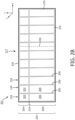
- FIGURES 2A and 2B schematically illustrate a dual-layer vertical detector configuration 200 of a multi-layer radiation sensitive detector array 120.
- the vertical detector 200 includes a slab or row of voxels 201.
- each row of detector voxels 201 includes the monolithic scintillator 124 with a first scintillator region 202 corresponding to a first scintillator layer 204, a second scintillator region 206 corresponding to a second scintillator layer 208, and an optically reflective barrier 210 there between, with the regions 202 and 206 and the optically reflective barrier 210 in a same physical scintillator material bulk 220.
- the optically reflective barrier 210 includes a major surface of a volume that separates the regions 202 and 206 and the major surface is parallel to a surface 250 receiving the incident radiation 117. In some instances, a position (e.g., depth) of the optically reflective barrier 210 in the bulk 220 maximizes an energy separation of the incident radiation.
- the physical bulk 220 receives the incident radiation 117, having traversed to the examination region 118, and converts the X-ray radiation to light radiation at a depth 230 in the bulk material 220 relative to an energy of the X-ray photons of the incident radiation 117.
- lower energy (shallow penetrating) X-ray photons are absorbed in the first region 202
- higher energy (deeper penetrating) X-ray photons are absorbed in the second region 206.
- Each of the regions 202 and 206 is optically coupled respectively to a different corresponding first and second photosensors 240 and 242 on a supporting substrate 244.
- the first scintillator region 202 of the scintillator bulk material 220 is optically coupled to the first photosensor 240 of an array of photosensors 246 and the second scintillator region 204 of the scintillator bulk material 220 is optically coupled to the second photosensor 242 of the array of photosensors 246.
- the array of photosensors 246 includes the first photosensor 240, the second photosensor 242 and the substrate 244.
- the array of photosensors 246 is disposed adjacent to the monolithic scintillator 124 and occupies a portion of the surface 250.
- the disposition of the array of photosensors 242 and the regions 202 and 206 relative to a direction of the incident X-ray radiation identifies the dual layer detector 200 as a vertical arrangement.
- FIGURE 2B schematically illustrates a side view of the scintillator side of one row of the detector voxels 201 of FIGURE 2A along the z-direction for a multi-row configuration.
- the same single physical scintillator material bulk 220 includes both scintillator regions of the dual layers for all for all of N rows of the multi-row configuration of the detector voxels 201, where N is a positive integer.
- the same physical scintillator material bulk 220 can be considered a slab of the scintillator material with scintillator voxel (or pixel) optical barriers 260 that define each scintillator voxel for each row, and the optically reflective barrier 210 defining the two scintillator regions 202 and 206 within each scintillator voxel.
- the detector surface area of one pixel corresponds to the detector volume of a plurality of voxel regions.
- the scintillator voxel optical barriers 260 are optically reflective barriers, similar to the optically reflective barrier 210, e.g., they include changes in the crystal structure of the same physical bulk material 220 induced by laser.
- the voxel optical barriers 260 define cuboid shaped voxels.
- the voxel optical barriers 260 define frustum of a square right pyramid shaped voxels.
- a thickness or depth (y-direction) of the optically reflective barrier 210 is dependent upon a diameter of a focal spot of the laser beam and a minimum thickness for optical separation according to the structure of altered scintillator material.
- the thickness of the optically reflective barrier 210 can be increased by a plurality of altered positions by the focal spot of the laser. That is, the altered positions are further altered in the y-direction, where a major surface the volume of the optically reflective barrier is altered extending in the x-z direction.
- the same physical scintillator material bulk 220 can include an outside or exterior surface 270, which is an optically reflective barrier induced by a laser.
- the outside surface is unchanged by laser and an optically reflective coating is applied.
- Combinations of the outside surface 270 altered to the optically reflective barrier and the optically reflective coating are contemplated.
- the dual layer detector array 200 illustrated in FIGURES 2A-2B is an MxN array of detector elements, with M slabs of scintillator material separated by the substrate 244 of the photosensor array 246 in a vertical arrangement, where M is a positive integer.
- Each slab includes N monolithic scintillator voxels within the same physical scintillator material bulk 220.
- An example of a vertical detector arrangement is discussed in US 9,000,382, filed October 29, 2009 , and entitle "Spectral Imaging Detector,".
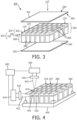
- the configuration 300 includes a single physical bulk 220 of monolithic scintillators 124. Each monolithic scintillator 124 includes the two regions 202 and 206.
- the single physical bulk 220 of monolithic scintillators 124 is disposed between substrates of two arrays of photosensors 310 and 320. Each of the two arrays of photosensors 310, 320 is disposed in a plane parallel to the surface 250 of the dual layer detector 300.
- the optically reflective barrier 210 of the same physical bulk 220 of scintillator material can include multiple sub-barriers such as two or more sub-barriers 330 and 332, which are separated from each other by a distance of 2-100 microns.
- Each of the barriers 330 and 332 includes a major surface of a volume defined by the barriers 330 and 332, which is substantially planar, with the major surface disposed parallel to the surface 250 of the dual layer detector 300.
- Each of the sub-barriers 330 and 332 includes changes to the crystal structure of the bulk material 220, induced by a laser beam.
- the optically reflective barrier comprises two barriers 330, 332 parallel to the surface 250 of the detector array configured to initially receive the X-ray radiation.
- the same physical scintillator material bulk 220 can include a plurality of individual monolithic scintillators 124 separated by the voxel optical barriers 260 and that form a multidimensional MxN array of voxels of the monolithic scintillators 124.
- the same physical scintillator material bulk 220 can include the optically reflective coating, the outside portion 270 of the same physical bulk 220 of the scintillator material altered structurally by laser to an optically reflective barrier, and combinations thereof.
- the arrays of photosensors 310 and 320 can include front illuminated photodiodes (FIP), back illuminated photodiodes (BIP), organic photodiodes (OPD), and combinations thereof.
- FIP front illuminated photodiodes
- BIP back illuminated photodiodes
- OPD organic photodiodes
- One or more of the arrays of photosensors 310, 320 can include a photodiode array that minimizes x-ray absorption, such as OPDs, aggressively thinned FIPs, aggressively thinned BIPs, x-ray transparent photosensors, etc.
- aggressively thinned means thinned to less than 30 microns.
- aggressively thinned means thinned to 30-100 microns.
- aggressively thinned means thinned to 100-200 microns.
- the array of photosensors 310 is optically coupled to the first layer 204 of the same physical bulk 220 of scintillator material, and corresponding photosensors 240 are dimensioned and aligned with corresponding the first regions 202 of each monolithic scintillator 124.
- the array of photosensors 320 opposite the first photosensor array 310 and the same physical bulk 220 of scintillator material is optically coupled to the second layer 206 of the same physical bulk 220 of scintillator material.
- the photosensors 244 of the second photosensor array 320 are dimensioned and aligned with corresponding second regions 206 of each voxel monolithic scintillator 124.
- a controller 400 controls the operation of one or more lasers 410, 420 and relative positioning of the lasers 410, 420 to the same physical bulk 220 of scintillator material positioned by a holder 430.
- a first laser 410 is positioned with a laser beam 412 oriented parallel to the optically reflective barrier 210.
- a second laser 420 is positioned with a laser beam 422 oriented perpendicular to the optically reflective barrier 210.
- one of the first laser 410 or the second laser 420 is omitted. In some embodiments, there are multiple lasers in either orientation.
- the laser beam 412, 422 is focused on a point 414 by at least one lens 416, 426.
- the point 414, 415 can be spherical in shape or elongated along the direction of the laser beam 412, 422.
- the point 414, 415 changes the crystal structure of the same physical bulk 220 of scintillator material according to the operating characteristics of the laser 410, 420.
- the operating characteristics of the laser 410, 420 are relative to the scintillator material. For example, wavelength, power and pulse can vary according to the scintillator material to achieve the change in crystal structure for the optically reflective barrier 210.
- the controller 400 moves the laser beam 412, 422 relative to the holder 430.
- the laser 410, 420 is fixed and the holder 430 moves.
- the laser 410, 420 moves and the holder 430 is fixed.
- both the laser 410, 420 and the holder 430 move.
- the first laser 410 is configured to move the point 414 across positions in a most distant plane of the same physical bulk 220 of scintillator material, and then proceed to positions in a next closest plane successively until changes of the crystal structure for the optically reflective barrier 210 and voxel optical barrier 260 are induced. That is, the point 414 remains between barriers already created and the laser.
- the barriers connect with orthogonal, oblique or non-parallel surfaces. That is, a major surface of a volume defining the optically reflective barrier 210 is non-parallel to a major surface of a volume defining the voxel optical barrier 260.
- FIGURE 5 a flowchart in accordance with an embodiment(s) herein is illustrated.
- the physical bulk 220 of scintillator material is positioned relative to one or more lasers 410, 420.
- the positioning can include receiving the physical bulk 220 of scintillator material in the holder 430.
- the positioning can include changes in position relative to the laser(s) to generate the optically reflective barrier 210 at a next location.
- the physical bulk 220 of scintillator material can include a volume of material for the monolithic scintillator 124 of a single voxel. In some embodiments, the physical bulk 220 of scintillator material can include a volume of material for a 1xN array of monolithic scintillators 124. In some embodiments, the physical bulk 220 of scintillator material can include a volume of material for an MxN array of monolithic scintillators 124.
- the holder is configured to hold combinations of the above.
- slabs of scintillator material for a one dimensional array of monolithic scintillators 124, or material for individual monolithic scintillator blocks 124 can be held together in the holder 430 for generating the optically reflective barrier 210 across mechanically separated slabs or across individually mechanically separated voxels.
- the crystal structure of a portion of the physical bulk 220 for monolithic scintillator blocks 124 is altered by a focused laser to define the plurality of regions in scintillator material for each voxel while maintaining the scintillator material as physically connected structure.
- the altered structural portion forming the optically reflective barrier 210 is oriented parallel to a surface 250 of the physical bulk 220 of scintillator material configured to initially receive the incident radiation 117.
- the altered structural portion of the monolithic scintillator 124 can include two or more barriers 330, 332 parallel to the surface 250 configured to initially receive the incident radiation 117.
- the optically reflective barrier comprises two barriers 330, 332 parallel to the surface 250 of the detector array configured to initially receive the X-ray radiation.
- the two barriers 330, 332 are parallel and separated by a distance between 2 microns and 100 microns. In some embodiments, the distance is between 25 and 100 microns.
- the altered structural portion further includes the voxel optical barrier 260 or a portion thereof.
- the altered portions further form a barrier perpendicular to the surface 250 configured to initially receive the incident radiation.
- the altered structural portion includes an outside surface 270, or a portion thereof, of the physical bulk 220 of scintillator material.
- Acts 500 and 510 are repeated with re-positioning and generating the altered structural portion until the monolithic scintillators 124 are formed.
- the controller 400 is configured to control the positioning and operation of the laser(s) to generate the altered structural portion at each position in a proper order to form the optically reflective barrier 210, and in some embodiments additionally the voxel optical barrier 260 and/or the reflective barrier 270 on the outside surface.
- the monolithic scintillators 124 are aligned with and affixed to one or more photosensor arrays.
- the monolithic scintillators 124 form 1xN dimensional array of voxels, and the monolithic scintillator 124 of each voxel includes the plurality of regions 202, 206 corresponding to layers 204, 208 defined by the optically reflective barrier 210.
- the photosensor array 246 is oriented perpendicular to a surface 250 of the multi-layer detector 120 which initially receives the incident radiation and aligned with and affixed to the physical bulk 220 of scintillator material.
- the first region 202 of each voxel aligns with the corresponding first photosensor 240 and the second region 206 of each voxel aligns with the corresponding second photosensor 242.
- the multi-layer detector array 120 as an MxN array of voxels can be further assembled with an assembly of M one dimensional arrays of voxels.
- the assembly can further include the addition of readout electronics 140.
- the assembly can further include the addition of a supporting substrate.
- the assembly can further include the application of a optically reflective coating.
- the generated monolithic scintillator blocks 124 formed from the structurally altered physical bulk 220 of the scintillator material include a two dimensional array of monolithic scintillators 124, and each monolithic scintillator 124 includes the plurality of regions 202, 206.
- the aligning and affixing includes aligning and affixing the generated monolithic scintillators 124 to a plurality of photosensor arrays 310, 320.
- Each of the plurality of photosensor arrays 310, 320 is oriented parallel to the surface 250 of the multi-layer detector that initially receives the incident radiation 117.
- the generated monolithic scintillators 124 formed from the structurally altered physical bulk 220 of the scintillator material are mechanically separated as individual monolithic scintillators 124, coated and re-assembled as either a 1xN array of monolithic scintillators 124 or an MxN array of monolithic scintillator 124.
- a monolithic scintillator 124 comprises: at least a first scintillator region 202, a second scintillator region 206, and an optically reflective barrier 210 therebetween, the optically reflective barrier comprises two barriers 330, 332 parallel to the surface 250 of the detector array configured to initially receive the X-ray radiation, a crystal structure of the two barriers of the optically reflective barrier has been structurally altered by laser, a material of the optically reflective barrier 210 between the two barriers of the optically reflective barrier 210 is of the same physical bulk as a material of the monolithic scintillator, and the material of the monolithic scintillator is a physically connected material.
- the operation of the controller 410 for positioning and operation of the lasers 410, 420 may be implemented by way of computer readable instructions, encoded or embedded on a computer readable storage medium, which, when executed by a computer processor(s), cause the processor(s) to carry out the described acts. Additionally or alternatively, at least one of the computer readable instructions is carried out by a signal, carrier wave or other transitory medium.
- the controller 410 includes an application specific integrated circuit.
Landscapes
- Health & Medical Sciences (AREA)
- Physics & Mathematics (AREA)
- General Physics & Mathematics (AREA)
- Life Sciences & Earth Sciences (AREA)
- High Energy & Nuclear Physics (AREA)
- Molecular Biology (AREA)
- Spectroscopy & Molecular Physics (AREA)
- Engineering & Computer Science (AREA)
- Chemical & Material Sciences (AREA)
- Power Engineering (AREA)
- Crystallography & Structural Chemistry (AREA)
- Condensed Matter Physics & Semiconductors (AREA)
- Radiology & Medical Imaging (AREA)
- Toxicology (AREA)
- Computer Hardware Design (AREA)
- Microelectronics & Electronic Packaging (AREA)
- Nuclear Medicine, Radiotherapy & Molecular Imaging (AREA)
- Pulmonology (AREA)
- Electromagnetism (AREA)
- Theoretical Computer Science (AREA)
- Analytical Chemistry (AREA)
- Biochemistry (AREA)
- General Health & Medical Sciences (AREA)
- Immunology (AREA)
- Pathology (AREA)
- Measurement Of Radiation (AREA)
- Apparatus For Radiation Diagnosis (AREA)
Claims (10)
- Réseau de détecteurs de tomodensitométrie (CT) (120) comprenant:
un scintillateur monolithique (124) qui comprend:au moins une première région scintillatrice (202),une seconde région scintillatrice (206), etune barrière optiquement réfléchissante (210) entre eux;dans lequel le réseau de détecteurs est configuré pour détecter un rayonnement de rayons X traversant une région d'examen et frappant le scintillateur monolithique et générer des premières données de projection indicatives d'une énergie de rayonnement de rayons x absorbée par la première région de scintillateur et des secondes données de projection indicatives d'une énergie d'un rayonnement de rayons x traversant la première région de scintillateur et absorbé par la seconde région de scintillateur, et dans lequel la barrière optiquement réfléchissante (210) est orientée parallèlement à une surface (250) du réseau de détecteurs configuré pour recevoir initialement un rayonnement de rayons X;et dans lequel la barrière optiquement réfléchissante comprend deux barrières (330, 332) parallèles à la surface (250) du réseau de détecteurs configurées pour recevoir initialement le rayonnement X, dans lequel les deux barrières de la barrière optiquement réfléchissante sont situées au niveau des parties extérieures de la barrière optiquement réfléchissante, dans laquelle une structure cristalline des deux barrières de la barrière optiquement réfléchissante a été structurellement modifiée par laser, et dans laquelle les deux barrières de la barrière optiquement réfléchissante sont séparées par une distance comprise entre 2 microns et 100 microns, et;un matériau de la barrière optiquement réfléchissante (210) entre les deux barrières de la barrière optiquement réfléchissante (210) ayant le même volume physique qu'un matériau du scintillateur monolithique, le matériau du scintillateur monolithique étant un matériau physiquement connecté. - Réseau de détecteurs (120) selon la revendication 1, dans lequel le scintillateur monolithique comprend une même masse physique de matériau scintillateur, et le matériau scintillateur comprend un matériau sélectionné dans un groupe constitué de:Oxysulfure de gadolinium (GOS, Gd2O2S),Grenat d'yttrium et d'aluminium (YAG, Y3Al5O12),Grenat d'yttrium et d'aluminium dopé au cérium (CE YAG, Ce Y3Al5O12),Grenat de gadolinium aluminium gallium (GAGG Gd3Al2GA3O12),Grenat de Gadolinium Aluminium Gallium dopé au cérium (CE GAGG, Ce Gd3Al2GA3O12), Séléniure de zinc (ZnSe), etTungstate de cadmium (CdWO4).
- Réseau de détecteurs (120) selon l'une des revendications 1-2, dans lequel le scintillateur monolithique comprend une partie d'un matériau scintillateur unique en vrac d'une pluralité d'éléments de détection, dans lequel chaque élément de détection comprend une première région de scintillateur et une deuxième région de scintillateur.
- Réseau de détecteurs (120) selon l'une quelconque des revendications 1-3, dans lequel le scintillateur monolithique est disposé de manière adjacente à un réseau de photocapteurs (244), dans lequel le réseau de photocapteurs est disposé dans un plan perpendiculaire à une surface (250) du réseau de détecteurs qui reçoit initialement le rayonnement X.
- Réseau de détecteurs (120) selon l'une quelconque des revendications 1-3, dans lequel le scintillateur monolithique est disposé entre deux réseaux de photocapteurs (310, 320), dans lequel chacun des deux réseaux de photocapteurs est disposé dans un plan parallèle à une surface (250) du réseau de détecteurs qui reçoit initialement un rayonnement de rayons X.
- Système de tomodensitométrie (100), comprenant:une source de rayonnement X (116) configurée pour émettre un rayonnement X qui traverse une région d'examen; etun réseau de détecteurs (120) selon l'une quelconque des revendications 1-5.
- Procédé de fabrication d'un appareil de détection de rayonnement par tomodensitométrie (CT), comprenant:modification d'une structure cristalline d'une partie (210) d'une masse physique unique (220) de matériau scintillateur par un laser focalisé (410, 420) pour définir une première pluralité de régions (202) et une seconde pluralité de régions d'un scintillateur monolithique tout en conservant la masse physique unique en tant que structure cristalline physiquement connectée, la première pluralité de régions (202) correspondant à une première couche (204) et la seconde pluralité de régions correspondant à une seconde couche (208), la partie modifiée étant entre la première couche et la seconde couche, et dans lequel la partie modifiée est orientée parallèlement à une surface (250) de l'appareil de détection configuré pour recevoir initialement un rayonnement X;dans lequel la partie de l'ensemble physique unique du matériau scintillateur modifié comprend deux barrières (330, 332) parallèles à la surface (250) du réseau de détecteurs configuré pour recevoir initialement le rayonnement X, dans lequel les deux barrières sont situées dans les parties extérieures de la partie de l'ensemble physique unique du matériau scintillateur modifié, dans lequel un matériau entre les deux barrières est du même volume physique qu'un matériau du scintillateur monolithique, dans lequel le matériau du scintillateur monolithique est un matériau physiquement connecté, et dans lequel les deux barrières sont séparées par une distance comprise entre 2 microns et 100 microns.
- Procédé selon la revendication 7, dans lequel la partie modifiée de la masse physique unique comprend en outre un volume (270) avec une surface qui est une surface extérieure de la masse physique unique.
- Procédé selon l'une quelconque des revendications 7-8, dans lequel la masse physique unique de matériau scintillateur comprend une pluralité de scintillateurs monolithiques dans un réseau unidimensionnel de scintillateurs monolithiques, chaque scintillateur monolithique comportant la pluralité de régions; et comprenant en outre:
aligner et fixer la masse physique unique de matériau scintillateur à un réseau de photocapteurs (244), le réseau de photocapteurs étant orienté perpendiculairement à la surface de l'appareil de détection configuré pour recevoir initialement un rayonnement de rayons X. - Procédé selon l'une quelconque des revendications 7-9, dans lequel la masse physique unique de matériau scintillateur comprend une pluralité de scintillateurs monolithiques dans un réseau bidimensionnel de scintillateurs, chaque scintillateur monolithique comportant deux régions; et comprenant en outre: aligner et fixer la masse physique unique de matériau scintillateur entre deux réseaux de photocapteurs (310, 320), chacun des deux réseaux de photocapteurs étant orienté parallèlement à la surface de l'appareil de détection configuré pour recevoir initialement un rayonnement de rayons X.
Applications Claiming Priority (2)
| Application Number | Priority Date | Filing Date | Title |
|---|---|---|---|
| US201762552563P | 2017-08-31 | 2017-08-31 | |
| PCT/EP2018/072383 WO2019042797A1 (fr) | 2017-08-31 | 2018-08-20 | Détecteur multicouche à scintillateur monolithique |
Publications (2)
| Publication Number | Publication Date |
|---|---|
| EP3676639A1 EP3676639A1 (fr) | 2020-07-08 |
| EP3676639B1 true EP3676639B1 (fr) | 2024-04-24 |
Family
ID=63294221
Family Applications (1)
| Application Number | Title | Priority Date | Filing Date |
|---|---|---|---|
| EP18758583.1A Active EP3676639B1 (fr) | 2017-08-31 | 2018-08-20 | Détecteur multicouche à scintillateur monolithique |
Country Status (5)
| Country | Link |
|---|---|
| US (1) | US11181488B2 (fr) |
| EP (1) | EP3676639B1 (fr) |
| JP (2) | JP7181283B2 (fr) |
| CN (1) | CN111133338A (fr) |
| WO (1) | WO2019042797A1 (fr) |
Families Citing this family (3)
| Publication number | Priority date | Publication date | Assignee | Title |
|---|---|---|---|---|
| CA3080643C (fr) | 2018-05-23 | 2021-06-15 | The Research Foundation For The State University Of New York | Imageur a rayons x a ecran plat avec substrat de verre scintillant |
| WO2023235270A1 (fr) * | 2022-05-31 | 2023-12-07 | University Of Washington | Détection codée pour tomodensitométrie à émission de photon unique |
| CN114878604A (zh) * | 2022-07-11 | 2022-08-09 | 芯晟捷创光电科技(常州)有限公司 | 一种射线探测器、探测方法和探测系统 |
Family Cites Families (18)
| Publication number | Priority date | Publication date | Assignee | Title |
|---|---|---|---|---|
| JP5268633B2 (ja) * | 2005-04-26 | 2013-08-21 | コーニンクレッカ フィリップス エレクトロニクス エヌ ヴィ | スペクトルctのための検出器アレイ |
| US7968853B2 (en) * | 2005-04-26 | 2011-06-28 | Koninklijke Philips Electronics N.V. | Double decker detector for spectral CT |
| RU2505840C2 (ru) | 2008-11-18 | 2014-01-27 | Конинклейке Филипс Электроникс Н.В. | Детектор спектральной визуализации |
| CN101937095B (zh) * | 2009-06-30 | 2012-05-09 | 同方威视技术股份有限公司 | 双能x射线探测器及双能x射线探测器阵列装置 |
| US9040924B2 (en) | 2009-10-27 | 2015-05-26 | University Of Washington Through Its Center For Commercialization | Optical-interface patterning for radiation detector crystals |
| US9513387B2 (en) | 2010-02-01 | 2016-12-06 | Siemens Aktiengesellschaft | System and method for providing depth of interaction detection using positron emission tomography |
| EP2671097B1 (fr) * | 2011-02-03 | 2016-10-19 | Koninklijke Philips N.V. | Détecteurs verticaux sensibles à un rayonnement à une ou à plusieurs énergies |
| CN103443652B (zh) | 2011-03-24 | 2017-02-15 | 皇家飞利浦有限公司 | 谱成像探测器 |
| US9411057B2 (en) * | 2011-04-01 | 2016-08-09 | Medtronic Navigation, Inc. | X-ray imaging system and method |
| EP2694999B1 (fr) * | 2011-04-06 | 2019-10-02 | Koninklijke Philips N.V. | Détecteur d'imagerie |
| WO2013080104A2 (fr) | 2011-12-02 | 2013-06-06 | Koninklijke Philips Electronics N.V. | Appareil de détection de rayonnement |
| US9012857B2 (en) * | 2012-05-07 | 2015-04-21 | Koninklijke Philips N.V. | Multi-layer horizontal computed tomography (CT) detector array with at least one thin photosensor array layer disposed between at least two scintillator array layers |
| JP2013246156A (ja) | 2012-05-29 | 2013-12-09 | Natl Inst Of Radiological Sciences | 3次元放射線位置検出器 |
| WO2015011587A1 (fr) * | 2013-07-23 | 2015-01-29 | Koninklijke Philips N.V. | Réseau de détecteurs imageurs (spectraux/non spectraux) hybride et éléments électroniques de traitement correspondants |
| WO2015131102A1 (fr) | 2014-02-28 | 2015-09-03 | The General Hospital Corporation | Système et procédé de traitement de détecteurs de rayonnement à l'aide de faisceaux laser |
| JP6529858B2 (ja) * | 2014-08-20 | 2019-06-12 | キヤノンメディカルシステムズ株式会社 | X線ct装置及びx線検出器 |
| JP6704737B2 (ja) | 2015-01-30 | 2020-06-03 | 浜松ホトニクス株式会社 | 放射線検出器 |
| CN108139491B (zh) | 2015-10-21 | 2022-06-07 | 皇家飞利浦有限公司 | 用于低能量辐射量子和高能量辐射量子的组合探测的辐射探测器 |
-
2018
- 2018-08-20 EP EP18758583.1A patent/EP3676639B1/fr active Active
- 2018-08-20 JP JP2020511809A patent/JP7181283B2/ja active Active
- 2018-08-20 WO PCT/EP2018/072383 patent/WO2019042797A1/fr unknown
- 2018-08-20 US US16/642,292 patent/US11181488B2/en active Active
- 2018-08-20 CN CN201880061019.3A patent/CN111133338A/zh active Pending
-
2022
- 2022-09-14 JP JP2022146094A patent/JP2022174229A/ja active Pending
Also Published As
| Publication number | Publication date |
|---|---|
| CN111133338A (zh) | 2020-05-08 |
| JP2020531183A (ja) | 2020-11-05 |
| US20210072167A1 (en) | 2021-03-11 |
| WO2019042797A1 (fr) | 2019-03-07 |
| JP2022174229A (ja) | 2022-11-22 |
| EP3676639A1 (fr) | 2020-07-08 |
| US11181488B2 (en) | 2021-11-23 |
| JP7181283B2 (ja) | 2022-11-30 |
Similar Documents
| Publication | Publication Date | Title |
|---|---|---|
| EP1876955B1 (fr) | Detecteur a double niveau pour tomographie spectrale par ordinateur | |
| US10371830B2 (en) | Radiation detector for combined detection of low-energy radiation quanta and high-energy radiation quanta | |
| US20190204460A1 (en) | Detector systems for integrated radiation imaging | |
| US7233640B2 (en) | CT detector having an optical mask layer | |
| US9012857B2 (en) | Multi-layer horizontal computed tomography (CT) detector array with at least one thin photosensor array layer disposed between at least two scintillator array layers | |
| EP3676639B1 (fr) | Détecteur multicouche à scintillateur monolithique | |
| JP5016180B2 (ja) | X線像取得装置 | |
| EP2926165B1 (fr) | Détecteur d'imagerie | |
| KR101898794B1 (ko) | 광자 계수형 검출기 | |
| US7211801B2 (en) | Radiation detector | |
| US6823038B2 (en) | X-ray detector array and method for manufacturing same | |
| US20150212216A1 (en) | Positron Emission Tomography and Single Photon Emission Computed Tomography based on Intensity Attenuation Shadowing Methods and Effects | |
| CN204241697U (zh) | 三维空间曲面多能量闪烁探测器 | |
| US20210278553A1 (en) | Three-dimensional solid state imaging photodetector | |
| EP3428691A1 (fr) | Détecteur de rayons x et son procédé de fabrication | |
| US20170184728A1 (en) | Scintillator configurations and methods for fabricating the same | |
| EP4095565A1 (fr) | Dispositif pour la détection de rayons gamma avec codification de profondeur d'interaction et temps de vol | |
| JPH11248843A (ja) | 2次元アレイ型放射線検出器 |
Legal Events
| Date | Code | Title | Description |
|---|---|---|---|
| STAA | Information on the status of an ep patent application or granted ep patent |
Free format text: STATUS: UNKNOWN |
|
| STAA | Information on the status of an ep patent application or granted ep patent |
Free format text: STATUS: THE INTERNATIONAL PUBLICATION HAS BEEN MADE |
|
| PUAI | Public reference made under article 153(3) epc to a published international application that has entered the european phase |
Free format text: ORIGINAL CODE: 0009012 |
|
| STAA | Information on the status of an ep patent application or granted ep patent |
Free format text: STATUS: REQUEST FOR EXAMINATION WAS MADE |
|
| 17P | Request for examination filed |
Effective date: 20200331 |
|
| AK | Designated contracting states |
Kind code of ref document: A1 Designated state(s): AL AT BE BG CH CY CZ DE DK EE ES FI FR GB GR HR HU IE IS IT LI LT LU LV MC MK MT NL NO PL PT RO RS SE SI SK SM TR |
|
| AX | Request for extension of the european patent |
Extension state: BA ME |
|
| DAV | Request for validation of the european patent (deleted) | ||
| DAX | Request for extension of the european patent (deleted) | ||
| STAA | Information on the status of an ep patent application or granted ep patent |
Free format text: STATUS: EXAMINATION IS IN PROGRESS |
|
| 17Q | First examination report despatched |
Effective date: 20220621 |
|
| GRAP | Despatch of communication of intention to grant a patent |
Free format text: ORIGINAL CODE: EPIDOSNIGR1 |
|
| STAA | Information on the status of an ep patent application or granted ep patent |
Free format text: STATUS: GRANT OF PATENT IS INTENDED |
|
| INTG | Intention to grant announced |
Effective date: 20231201 |
|
| GRAS | Grant fee paid |
Free format text: ORIGINAL CODE: EPIDOSNIGR3 |
|
| GRAA | (expected) grant |
Free format text: ORIGINAL CODE: 0009210 |
|
| STAA | Information on the status of an ep patent application or granted ep patent |
Free format text: STATUS: THE PATENT HAS BEEN GRANTED |
|
| AK | Designated contracting states |
Kind code of ref document: B1 Designated state(s): AL AT BE BG CH CY CZ DE DK EE ES FI FR GB GR HR HU IE IS IT LI LT LU LV MC MK MT NL NO PL PT RO RS SE SI SK SM TR |
|
| REG | Reference to a national code |
Ref country code: GB Ref legal event code: FG4D |
|
| REG | Reference to a national code |
Ref country code: CH Ref legal event code: EP |
|
| REG | Reference to a national code |
Ref country code: DE Ref legal event code: R096 Ref document number: 602018068555 Country of ref document: DE |
|
| REG | Reference to a national code |
Ref country code: IE Ref legal event code: FG4D |