EP3675304B1 - Control device for 3-terminal static dc transformer - Google Patents
Control device for 3-terminal static dc transformer Download PDFInfo
- Publication number
- EP3675304B1 EP3675304B1 EP18848068.5A EP18848068A EP3675304B1 EP 3675304 B1 EP3675304 B1 EP 3675304B1 EP 18848068 A EP18848068 A EP 18848068A EP 3675304 B1 EP3675304 B1 EP 3675304B1
- Authority
- EP
- European Patent Office
- Prior art keywords
- voltage
- terminal
- self
- terminals
- extinguishing
- Prior art date
- Legal status (The legal status is an assumption and is not a legal conclusion. Google has not performed a legal analysis and makes no representation as to the accuracy of the status listed.)
- Active
Links
Images

Classifications
-
- H—ELECTRICITY
- H02—GENERATION; CONVERSION OR DISTRIBUTION OF ELECTRIC POWER
- H02M—APPARATUS FOR CONVERSION BETWEEN AC AND AC, BETWEEN AC AND DC, OR BETWEEN DC AND DC, AND FOR USE WITH MAINS OR SIMILAR POWER SUPPLY SYSTEMS; CONVERSION OF DC OR AC INPUT POWER INTO SURGE OUTPUT POWER; CONTROL OR REGULATION THEREOF
- H02M1/00—Details of apparatus for conversion
- H02M1/36—Means for starting or stopping converters
-
- H—ELECTRICITY
- H02—GENERATION; CONVERSION OR DISTRIBUTION OF ELECTRIC POWER
- H02M—APPARATUS FOR CONVERSION BETWEEN AC AND AC, BETWEEN AC AND DC, OR BETWEEN DC AND DC, AND FOR USE WITH MAINS OR SIMILAR POWER SUPPLY SYSTEMS; CONVERSION OF DC OR AC INPUT POWER INTO SURGE OUTPUT POWER; CONTROL OR REGULATION THEREOF
- H02M3/00—Conversion of DC power input into DC power output
- H02M3/22—Conversion of DC power input into DC power output with intermediate conversion into AC
- H02M3/24—Conversion of DC power input into DC power output with intermediate conversion into AC by static converters
- H02M3/28—Conversion of DC power input into DC power output with intermediate conversion into AC by static converters using discharge tubes with control electrode or semiconductor devices with control electrode to produce the intermediate AC
- H02M3/325—Conversion of DC power input into DC power output with intermediate conversion into AC by static converters using discharge tubes with control electrode or semiconductor devices with control electrode to produce the intermediate AC using devices of a triode or a transistor type requiring continuous application of a control signal
- H02M3/335—Conversion of DC power input into DC power output with intermediate conversion into AC by static converters using discharge tubes with control electrode or semiconductor devices with control electrode to produce the intermediate AC using devices of a triode or a transistor type requiring continuous application of a control signal using semiconductor devices only
- H02M3/33561—Conversion of DC power input into DC power output with intermediate conversion into AC by static converters using discharge tubes with control electrode or semiconductor devices with control electrode to produce the intermediate AC using devices of a triode or a transistor type requiring continuous application of a control signal using semiconductor devices only having more than one ouput with independent control
-
- H—ELECTRICITY
- H02—GENERATION; CONVERSION OR DISTRIBUTION OF ELECTRIC POWER
- H02M—APPARATUS FOR CONVERSION BETWEEN AC AND AC, BETWEEN AC AND DC, OR BETWEEN DC AND DC, AND FOR USE WITH MAINS OR SIMILAR POWER SUPPLY SYSTEMS; CONVERSION OF DC OR AC INPUT POWER INTO SURGE OUTPUT POWER; CONTROL OR REGULATION THEREOF
- H02M3/00—Conversion of DC power input into DC power output
- H02M3/22—Conversion of DC power input into DC power output with intermediate conversion into AC
- H02M3/24—Conversion of DC power input into DC power output with intermediate conversion into AC by static converters
- H02M3/28—Conversion of DC power input into DC power output with intermediate conversion into AC by static converters using discharge tubes with control electrode or semiconductor devices with control electrode to produce the intermediate AC
- H02M3/325—Conversion of DC power input into DC power output with intermediate conversion into AC by static converters using discharge tubes with control electrode or semiconductor devices with control electrode to produce the intermediate AC using devices of a triode or a transistor type requiring continuous application of a control signal
- H02M3/335—Conversion of DC power input into DC power output with intermediate conversion into AC by static converters using discharge tubes with control electrode or semiconductor devices with control electrode to produce the intermediate AC using devices of a triode or a transistor type requiring continuous application of a control signal using semiconductor devices only
- H02M3/33569—Conversion of DC power input into DC power output with intermediate conversion into AC by static converters using discharge tubes with control electrode or semiconductor devices with control electrode to produce the intermediate AC using devices of a triode or a transistor type requiring continuous application of a control signal using semiconductor devices only having several active switching elements
- H02M3/33576—Conversion of DC power input into DC power output with intermediate conversion into AC by static converters using discharge tubes with control electrode or semiconductor devices with control electrode to produce the intermediate AC using devices of a triode or a transistor type requiring continuous application of a control signal using semiconductor devices only having several active switching elements having at least one active switching element at the secondary side of an isolation transformer
-
- H—ELECTRICITY
- H02—GENERATION; CONVERSION OR DISTRIBUTION OF ELECTRIC POWER
- H02M—APPARATUS FOR CONVERSION BETWEEN AC AND AC, BETWEEN AC AND DC, OR BETWEEN DC AND DC, AND FOR USE WITH MAINS OR SIMILAR POWER SUPPLY SYSTEMS; CONVERSION OF DC OR AC INPUT POWER INTO SURGE OUTPUT POWER; CONTROL OR REGULATION THEREOF
- H02M7/00—Conversion of AC power input into DC power output; Conversion of DC power input into AC power output
- H02M7/42—Conversion of DC power input into AC power output without possibility of reversal
- H02M7/44—Conversion of DC power input into AC power output without possibility of reversal by static converters
- H02M7/48—Conversion of DC power input into AC power output without possibility of reversal by static converters using discharge tubes with control electrode or semiconductor devices with control electrode
- H02M7/53—Conversion of DC power input into AC power output without possibility of reversal by static converters using discharge tubes with control electrode or semiconductor devices with control electrode using devices of a triode or transistor type requiring continuous application of a control signal
- H02M7/537—Conversion of DC power input into AC power output without possibility of reversal by static converters using discharge tubes with control electrode or semiconductor devices with control electrode using devices of a triode or transistor type requiring continuous application of a control signal using semiconductor devices only, e.g. single switched pulse inverters
- H02M7/5387—Conversion of DC power input into AC power output without possibility of reversal by static converters using discharge tubes with control electrode or semiconductor devices with control electrode using devices of a triode or transistor type requiring continuous application of a control signal using semiconductor devices only, e.g. single switched pulse inverters in a bridge configuration
Definitions
- the present invention generally relates to a control device, and in particular can be suitably applied to a control device which controls the drive of a three-terminal static DC converter to which three DC terminals are connected via a high-frequency alternating current.
- a two-terminal static converter known as a solid state transformer, which converts DC into a high-frequency AC voltage, boosts or drops the high-frequency AC voltage via an AC converter, and thereafter once again converts the AC voltage into DC
- a three-terminal static converter capable of safely expanding the connection (this is hereinafter referred to as a "three-terminal static DC converter"), rather than a two-terminal static converter, is desirable.
- a three-terminal static DC converter is a device that is used when performing DC distribution or the like, and comprises first to third DC terminals in which bridge circuits respectively configured from four self-extinguishing elements and DC capacitors are connected in parallel, and is a DC converter capable of mutually accommodating power among the first to third DC terminals.
- PTL 1 discloses charging the DC capacitors of the respective terminals by using a pre-charge circuit which is normally provided separately.
- PTL 2 discloses a method of inserting a resistor into a main circuit which controls the drive of a three-terminal static converter, charging the DC capacitors with a current that is limited by resistance, and short circuiting the resistor after the charging is complete.
- the present invention was devised in view of the foregoing points, and an object of this invention is to propose a control device capable of safely activating a three-terminal static DC converter while suppressing the increase in the size of the device comprising the three-terminal static DC converter as well as the increase in product cost.
- the dependent claim contains an advantageous embodiment of the present invention.
- control device capable of safely activating a three-terminal static DC converter while suppressing the increase in the size of the device comprising the three-terminal static DC converter as well as the increase in product cost.
- reference numeral 1 shows a three-terminal static DC converter as a whole according to this embodiment.
- the three-terminal static DC converter 1 is configured by comprising a first bridge circuit 3A and a first DC capacitor 4A connected in parallel between first and second terminals 2AA, 2AB configuring a first DC terminal 2A, a second bridge circuit 3B and a second DC capacitor 4B connected in parallel between first and second terminals 2BA, 2BB configuring a second DC terminal 2B, a third bridge circuit 3C and a third DC capacitor 4C connected in parallel between first and second terminals 2CA, 2CB configuring a third DC terminal 2C, and a three-winding wire high frequency transformer 5 which connects the first to third bridge circuits 3A to 3C.
- the first bridge circuit 3A is configured from a single phase inverter (also referred to as “self-excited single phase inverter”) in which first to fourth self-extinguishing elements 10A to 13A as typified by IGBT (Insulated Gate Bipolar Transistors) or power MOSFET (Metal-Oxide-Semiconductor Field-Effect Transistors) are connected in a bridge shape, and first to fourth diodes 14A to 17A are respectively connected in parallel to the first to fourth self-extinguishing elements 10A to 13A.
- IGBT Insulated Gate Bipolar Transistors
- MOSFET Metal-Oxide-Semiconductor Field-Effect Transistors
- connection midpoint of the first and fourth self-extinguishing elements 10A, 13A is connected to the first terminal 2AA of the first DC terminal 2A, and a connection midpoint of the second and third self-extinguishing elements 11A, 12A is connected to the second terminal 2AB of the first DC terminal 2A.
- the second bridge circuit 3B is configured from a single phase inverter in which first to fourth self-extinguishing elements 10B to 13B are connected in a bridge shape, and first to fourth diodes 14B to 17B are respectively connected in parallel to the first to fourth self-extinguishing elements 10B to 13B. Furthermore, with the second bridge circuit 3B, a connection midpoint of the first and fourth self-extinguishing elements 10B, 13B is connected to the first terminal 2BA of the second DC terminal 2B, and a connection midpoint of the second and third self-extinguishing elements 11B, 12B is connected to the second terminal 2BB of the second DC terminal 2B.
- the third bridge circuit 3C is configured from a single phase inverter in which first to fourth self-extinguishing elements 10C to 13C are connected in a bridge shape, and first to fourth diodes 14C to 17C are respectively connected in parallel to the first to fourth self-extinguishing elements 10C to 13C. Furthermore, with the third bridge circuit 3C, a connection midpoint of the first and fourth self-extinguishing elements 10C, 13C is connected to the first terminal 2CA of the third DC terminal 2C, and a connection midpoint of the second and third self-extinguishing elements 11C, 12C is connected to the second terminal 2CB of the third DC terminal 2C.
- the three-winding wire high frequency transformer 5 is configured by comprising first to third winding wires 18A to 18C wound around an iron core 19.
- the first winding wire 18A is connected between the connection midpoint of the first and second self-extinguishing elements 10A, 11A and the connection midpoint of the third and fourth self-extinguishing elements 12A, 13A in the first bridge circuit 3A.
- the second winding wire 18B is connected between the connection midpoint of the first and second self-extinguishing elements 10B, 11B and the connection midpoint of the third and fourth self-extinguishing elements 12B, 13B in the second bridge circuit 3B
- the third winding wire 18C is connected between the connection midpoint of the first and second self-extinguishing elements 10C, 11C and the connection midpoint of the third and fourth self-extinguishing elements 12C, 13C in the third bridge circuit 3C.
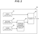
- Fig. 2 shows the configuration of a control device 20 according to this embodiment which controls the operation of the first to third bridge circuits 3A to 3C during the normal operation of the three-terminal static DC converter 1.
- the control device 20 is configured by comprising first to third detectors 21 to 23, a minimum voltage terminal detection circuit 24, and an arithmetic circuit 25.
- the first detector 21 is a voltage detector which detects a voltage Ed1 between the first and second terminals 2AA, 2AB of the first DC terminal 2A, and outputs the detected voltage Ed1, as first voltage information, to the arithmetic circuit 25.
- the second detector 22 is a voltage detector which detects a voltage Ed2 between the first and second terminals 2BA, 2BB of the second DC terminal 2B, and outputs the detected voltage Ed2, as second voltage information, to the minimum voltage terminal detection circuit 24.
- the third detector 23 is a voltage detector which detects a voltage Ed3 between the first and second terminals 2CA, 2CB of the third DC terminal 2C, and outputs the detected voltage Ed3, as third voltage information, to the minimum voltage terminal detection circuit 24.
- the minimum voltage terminal detection circuit 24 has a function of selecting the lower voltage (voltage Ed2 or voltage Ed3) of either the voltage Ed2 between the first and second terminals 2BA, 2BB of the second DC terminal 2B and the voltage Ed3 between the first and second terminals 2CA, 2CB of the third DC terminal 2C, which form an output-side terminal pair of the three-terminal static DC converter 1 of this embodiment, and notifying the selected lower voltage (voltage Ed2 or voltage Ed3) to the arithmetic circuit 25.
- the minimum voltage terminal detection circuit 24 selects the second or third voltage information, whichever is of a lower voltage, based on the second voltage information provided by the second detector 22 and the third voltage information provided by the third detector 23, and transfers the selected second or third voltage information to the arithmetic circuit 25.
- the arithmetic circuit 25 has a function of controlling the charging of the second and third DC capacitors 4B, 4C connected respectively to the second and third bridge circuits 3B, 3C based on the first voltage information provided by the first detector 21 and the second or third voltage information provided by the minimum voltage terminal detection circuit 24.
- the arithmetic circuit 25 by sending first to fourth on-pulse signals S1 to S4 respectively to the first to fourth self-extinguishing elements 10A to 13A of the first bridge circuit 3A and driving the first to fourth self-extinguishing elements 10A to 13A at the required timing, generates potential differences (voltage Ed2, Ed3) respectively between the first and second terminals 2BA, 2BB of the second DC terminal 2B and between the first and second terminals 2CA, 2CB of the third DC terminal 2C, and thereby charges the second and third DC capacitors 4B, 4C.
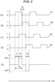
- Fig. 3(A) to Fig. 3(D) show waveform examples of the first to fourth on-pulse signals S1 to S4 provided respectively from the arithmetic circuit 25 to the first to fourth self-extinguishing elements 10A to 13A of the first bridge circuit 3A upon activation of the three-terminal static DC converter 1.
- the arithmetic circuit 25 does not provide the first to fourth on-pulse signals to the first to fourth self-extinguishing elements 10B to 13B, 10C to 13C of the second and third bridge circuits 3B, 3C to keep the first to fourth self-extinguishing elements 10B to 13B, 10C to 13C of the second and third bridge circuits 3B, 3C in an OFF state, and only the respective first to fourth diodes 14B to 17B, 14C to 17C connected in parallel to the first to fourth self-extinguishing elements 10B to 13B, 10C to 13C are operated.
- the arithmetic circuit 25 upon activation of the three-terminal static DC converter 1, causes the first and second self-extinguishing elements 10A, 11A of the first bridge circuit 3A to operate at 50% of the conduction duty ratio.
- a dead time Td is secured between the ON period of the first self-extinguishing element 10A and the ON period of the second self-extinguishing element 11A.
- the "ON period" of the first self-extinguishing element 10A and the second self-extinguishing element 11A is the period that the first self-extinguishing element 10A and the second self-extinguishing element 11A are turned ON and operated as a result of the first on-pulse signal S1 and the second on-pulse signal S2 rise to a logical "1" level.
- the same also applies to the third and fourth self-extinguishing elements 12A, 13A.
- the arithmetic circuit 25 also causes the third and fourth self-extinguishing elements 12A, 13A of the first bridge circuit 3A to operate at 50% of the conduction duty ratio. Even in the foregoing case, in order to avoid a DC short circuit, a dead time Td is secured between the ON period of the third self-extinguishing element 12A and the ON period of the fourth self-extinguishing element 13A.
- the arithmetic circuit 25 adjusts the phases of the first to fourth on-pulse signals S1 to S4 so that the foregoing ON period of the first self-extinguishing element 10A and the ON period of the third self-extinguishing element 12A periodically overlap for only a given period of time, and so that the ON period of the second self-extinguishing element 11A and the ON period of the fourth self-extinguishing element 13A regularly overlap only for a given period of time.
- a current will flow into the third DC capacitor 4C (that is, a potential difference Ed3 will be generated between the first and second terminals 2CA, 2CB of the third DC terminal 2C) via the second diode 15C, the third winding wire 18C and the fourth diode 17C, or via the third diode 16C, the third winding wire 18C and the first diode 14C, and the third DC capacitor 4C is thereby charged.
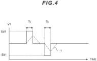
- the first and third self-extinguishing elements 10A, 12A are simultaneously turned ON and operated, and during other times the second and fourth self-extinguishing elements 11A, 13A are simultaneously turned ON and operated. Consequently, a voltage V1 of a size of "Ed1" or "-Ed1" will alternately appear in the first winding wire 18A of the three-winding wire high frequency transformer 5 at half the cycle that the first to fourth self-extinguishing elements 10A to 13A is turned ON/OFF.
- Ip 1 L ⁇ 0 Tc Ed 1 dt
- the maximum value Ip is equal to or less than the ampacity of the first to fourth self-extinguishing elements 10B to 13B, 10C to 13C configuring the second and third bridge circuits 3B, 3C.
- the size of the current I2, I3 that will flow to the second bridge circuit 3B and the third bridge circuit 3C will be determined based on the size of the voltage Ed2, Ed3 that appears in the second or third DC terminal 2B, 2C. Accordingly, upon determining the current value Im, the current value Im needs to be kept to a size that is equal to or less than the current rating of the first to fourth self-extinguishing elements 10B to 13B, 10C to 13C configuring the second or third bridge circuit 3B, 3C connected to the second or third DC terminal 2B, 2C in which a higher voltage will appear.
- the maximum value of the ON period T may be obtained by applying, as the denominator, (Ed1 - Ed2) or (Ed1 - Ed3) in substitute for "Ed1" on the right side of Formula (3).
- the greater potential (Ed1 - Ed2" or "Ed1 - Ed3" should be selected.
- the arithmetic circuit 25 of the control device 20 selects the smaller of either voltages Ed2, Ed3 detected respectively by the second detector 22 and the third detector 23, and computes the conduction period Tc of the first bridge circuit 3A based on the following formula.
- Tc L ⁇ Im Ed 1 ⁇ Min Ed 2 , Ed 3
- delay time ⁇ means the delay time of the period that the third on-pulse signal S3 rises to the logical "1" level relative to the period that the first on-pulse signal S1 rises to the logical "1” level, and the delay time of the period that the fourth on-pulse signal S4 rises to the logical "1” level relative to the period that the second on-pulse signal S2 rises to the logical "1" level.
- the arithmetic circuit 25 controls the size of the current I1 that flows to the first winding wire 18A of the three-winding wire high frequency transformer 5, which controls the delay time ⁇ of the third on-pulse signal S3 relative to the first on-pulse signal S1 or the delay time ⁇ of the fourth on-pulse signal S4 relative to the second on-pulse signal S2, and thereby controls the size of the current I2, I3 to flow to the second and third winding wires 18B, 18C of the three-winding wire high frequency transformer 5, and eventually to the second and third bridge circuits 3B, 3C.
- the second DC capacitor 4B connected to the second DC terminal 2B and the third DC capacitor 4C to the third DC terminal 2C are charged based on the control of the control device 20 which controls the drive of the first to third bridge circuits 3A to 3C during the normal operation of the three-terminal static DC converter 1. Accordingly to this embodiment, there is no need to separately prepare circuits or devices for activating the three-terminal static DC converter 1, which are not used during normal operation, and the overall cost can be reduced by that much.
- control device 20 controls the delay time ⁇ of the first to fourth on-pulse signals S1 to S4 so that the size of the currents I2, I3 which respectively flow to the second and third winding wires 18B, 18C of the three-winding wire high frequency transformer 5 due to the current I1 flowing to the first winding wire 18A of the three-winding wire high frequency transformer 5 to be equal to or less than the current rating of the first to fourth self-extinguishing elements 10B to 13B, 10C to 13C configuring the second and third bridge circuits 3B, 3C.
- the three-winding wire high frequency transformer 5 can be safely activated without damaging the first to fourth self-extinguishing elements 10B to 13B configuring the second bridge circuit 3B and the first to fourth self-extinguishing elements 10C to 13C configuring the third bridge circuit 3C.
- control device capable of safely activating a three-terminal static DC converter while suppressing the increase in the size of the device comprising the three-terminal static DC converter as well as the increase in product cost.
- the present invention is not limited thereto, and can be broadly applied to a multi-terminal static DC converter configured such that three or more single phase inverters, to which DC capacitors are respectively connected in parallel on a DC side, are connected on an AC side via a high frequency transformer having winding wires in a quantity corresponding to a number of the single phase inverters, and power can be accommodated among three or more DC terminals to which the corresponding single phase inverters are respectively connected.
Landscapes
- Engineering & Computer Science (AREA)
- Power Engineering (AREA)
- Inverter Devices (AREA)
- Dc-Dc Converters (AREA)
- Direct Current Feeding And Distribution (AREA)
Description
- The present invention generally relates to a control device, and in particular can be suitably applied to a control device which controls the drive of a three-terminal static DC converter to which three DC terminals are connected via a high-frequency alternating current.
- In recent years, as countermeasures against global warming, the use of renewable energy as typified by solar power generation is increasing across the globe, and consequently the use of secondary batteries for storing renewable energy is also increasing. Moreover, the use of fuel cells that generate electricity from natural gas has also begun. Because solar power generators, secondary batteries and fuel cells generate or store power via DC, the power output therefrom is used by being converted into AC via an inverter.
- Nevertheless, under circumstances where the use of renewable energy is expected to increase in the future, the introduction of DC power transmission or DC distribution, in which the power output from solar power generators and the like is used as is without being converted into AC, is expected. This is based on the background that inverters are now inexpensive and highly reliable due to the development of self-extinguishing semiconductor devices in which their ON/OFF can be arbitrarily switched based on external signals, and the research and development of DC transmission and DC distribution as the next-generation distribution system are underway.
- Meanwhile, when connecting different voltages via DC, a two-terminal static converter known as a solid state transformer, which converts DC into a high-frequency AC voltage, boosts or drops the high-frequency AC voltage via an AC converter, and thereafter once again converts the AC voltage into DC, is broadly used. Nevertheless, when using a converter in a DC distribution system, the adoption of a three-terminal static converter capable of safely expanding the connection (this is hereinafter referred to as a "three-terminal static DC converter"), rather than a two-terminal static converter, is desirable.
- A three-terminal static DC converter is a device that is used when performing DC distribution or the like, and comprises first to third DC terminals in which bridge circuits respectively configured from four self-extinguishing elements and DC capacitors are connected in parallel, and is a DC converter capable of mutually accommodating power among the first to third DC terminals.
- With this kind of three-terminal static converter, it is necessary to charge the respective DC capacitors connected to each of the DC terminals before operation, and maintain the voltage of these DC terminals at a predetermined voltage. As a method therefor, for example,
PTL 1 discloses charging the DC capacitors of the respective terminals by using a pre-charge circuit which is normally provided separately. Moreover, PTL 2 discloses a method of inserting a resistor into a main circuit which controls the drive of a three-terminal static converter, charging the DC capacitors with a current that is limited by resistance, and short circuiting the resistor after the charging is complete. -
- [PTL 1]
Japanese Unexamined Patent Application Publication No. H11-196529 - [PTL 2]
Japanese Unexamined Patent Application Publication No. 2008-259253 - Meanwhile, conventionally, the charging of three DC capacitors required for activating the three-terminal static converter was performed using circuits or devices other than the main circuit described above. Nevertheless, because these circuits or devices are not used during the normal operation of a three-terminal static converter, there was a problem in that the size of the overall device comprising the three-terminal static converter, and the product cost thereof, would increase.
- Moreover, when activating a three-terminal static converter, it is important that the three-terminal static converter can be activated safely without being damaged.
- The present invention was devised in view of the foregoing points, and an object of this invention is to propose a control device capable of safely activating a three-terminal static DC converter while suppressing the increase in the size of the device comprising the three-terminal static DC converter as well as the increase in product cost.
- This object is solved by the features of the independent claim. The dependent claim contains an advantageous embodiment of the present invention.
- According to the present invention, it is possible to realize a control device capable of safely activating a three-terminal static DC converter while suppressing the increase in the size of the device comprising the three-terminal static DC converter as well as the increase in product cost.
-
- [
Fig. 1 ]
Fig. 1 is a circuit diagram showing the three-terminal static DC converter according to this embodiment. - [
Fig. 2 ]
Fig. 2 is a block diagram showing a partial configuration of the control device which controls the three-terminal static DC converter ofFig. 1 . - [
Fig. 3 ]
Fig. 3(A) to Fig. 3(D) are waveform diagrams showing waveform examples of the first to fourth on-pulse signals, andFig. 3(E) is a waveform diagram showing a waveform example of the AC voltage generated in the first bridge circuit. - [
Fig. 4 ]
Fig. 4 is a waveform diagram showing waveform examples of the AC voltage and the AC current generated in the first bridge circuit. - An embodiment of the present invention is now explained in detail with reference to the appended drawings.
- In
Fig. 1 ,reference numeral 1 shows a three-terminal static DC converter as a whole according to this embodiment. The three-terminalstatic DC converter 1 is configured by comprising afirst bridge circuit 3A and afirst DC capacitor 4A connected in parallel between first and second terminals 2AA, 2AB configuring afirst DC terminal 2A, asecond bridge circuit 3B and asecond DC capacitor 4B connected in parallel between first and second terminals 2BA, 2BB configuring asecond DC terminal 2B, athird bridge circuit 3C and athird DC capacitor 4C connected in parallel between first and second terminals 2CA, 2CB configuring athird DC terminal 2C, and a three-winding wirehigh frequency transformer 5 which connects the first tothird bridge circuits 3A to 3C. - The
first bridge circuit 3A is configured from a single phase inverter (also referred to as "self-excited single phase inverter") in which first to fourth self-extinguishingelements 10A to 13A as typified by IGBT (Insulated Gate Bipolar Transistors) or power MOSFET (Metal-Oxide-Semiconductor Field-Effect Transistors) are connected in a bridge shape, and first tofourth diodes 14A to 17A are respectively connected in parallel to the first to fourth self-extinguishingelements 10A to 13A. - With the
first bridge circuit 3A, a connection midpoint of the first and fourth self-extinguishingelements first DC terminal 2A, and a connection midpoint of the second and third self-extinguishingelements first DC terminal 2A. - Similarly, the
second bridge circuit 3B is configured from a single phase inverter in which first to fourth self-extinguishing elements 10B to 13B are connected in a bridge shape, and first tofourth diodes 14B to 17B are respectively connected in parallel to the first to fourth self-extinguishing elements 10B to 13B. Furthermore, with thesecond bridge circuit 3B, a connection midpoint of the first and fourth self-extinguishingelements second DC terminal 2B, and a connection midpoint of the second and third self-extinguishingelements second DC terminal 2B. - Moreover, the
third bridge circuit 3C is configured from a single phase inverter in which first to fourth self-extinguishing elements 10C to 13C are connected in a bridge shape, and first tofourth diodes 14C to 17C are respectively connected in parallel to the first to fourth self-extinguishing elements 10C to 13C. Furthermore, with thethird bridge circuit 3C, a connection midpoint of the first and fourth self-extinguishingelements third DC terminal 2C, and a connection midpoint of the second and third self-extinguishingelements third DC terminal 2C. - The three-winding wire
high frequency transformer 5 is configured by comprising first tothird winding wires 18A to 18C wound around aniron core 19. Thefirst winding wire 18A is connected between the connection midpoint of the first and second self-extinguishingelements elements first bridge circuit 3A. Moreover, the second windingwire 18B is connected between the connection midpoint of the first and second self-extinguishingelements elements second bridge circuit 3B, and thethird winding wire 18C is connected between the connection midpoint of the first and second self-extinguishingelements elements third bridge circuit 3C. -
Fig. 2 shows the configuration of acontrol device 20 according to this embodiment which controls the operation of the first tothird bridge circuits 3A to 3C during the normal operation of the three-terminalstatic DC converter 1. Thecontrol device 20 is configured by comprising first tothird detectors 21 to 23, a minimum voltage terminal detection circuit 24, and anarithmetic circuit 25. - The
first detector 21 is a voltage detector which detects a voltage Ed1 between the first and second terminals 2AA, 2AB of thefirst DC terminal 2A, and outputs the detected voltage Ed1, as first voltage information, to thearithmetic circuit 25. Moreover, thesecond detector 22 is a voltage detector which detects a voltage Ed2 between the first and second terminals 2BA, 2BB of thesecond DC terminal 2B, and outputs the detected voltage Ed2, as second voltage information, to the minimum voltage terminal detection circuit 24. Furthermore, thethird detector 23 is a voltage detector which detects a voltage Ed3 between the first and second terminals 2CA, 2CB of thethird DC terminal 2C, and outputs the detected voltage Ed3, as third voltage information, to the minimum voltage terminal detection circuit 24. - The minimum voltage terminal detection circuit 24 has a function of selecting the lower voltage (voltage Ed2 or voltage Ed3) of either the voltage Ed2 between the first and second terminals 2BA, 2BB of the
second DC terminal 2B and the voltage Ed3 between the first and second terminals 2CA, 2CB of thethird DC terminal 2C, which form an output-side terminal pair of the three-terminalstatic DC converter 1 of this embodiment, and notifying the selected lower voltage (voltage Ed2 or voltage Ed3) to thearithmetic circuit 25. In effect, the minimum voltage terminal detection circuit 24 selects the second or third voltage information, whichever is of a lower voltage, based on the second voltage information provided by thesecond detector 22 and the third voltage information provided by thethird detector 23, and transfers the selected second or third voltage information to thearithmetic circuit 25. - The
arithmetic circuit 25 has a function of controlling the charging of the second andthird DC capacitors third bridge circuits first detector 21 and the second or third voltage information provided by the minimum voltage terminal detection circuit 24. - In effect, the
arithmetic circuit 25, by sending first to fourth on-pulse signals S1 to S4 respectively to the first to fourth self-extinguishingelements 10A to 13A of thefirst bridge circuit 3A and driving the first to fourth self-extinguishingelements 10A to 13A at the required timing, generates potential differences (voltage Ed2, Ed3) respectively between the first and second terminals 2BA, 2BB of thesecond DC terminal 2B and between the first and second terminals 2CA, 2CB of thethird DC terminal 2C, and thereby charges the second andthird DC capacitors -
Fig. 3(A) to Fig. 3(D) show waveform examples of the first to fourth on-pulse signals S1 to S4 provided respectively from thearithmetic circuit 25 to the first to fourth self-extinguishingelements 10A to 13A of thefirst bridge circuit 3A upon activation of the three-terminalstatic DC converter 1. - Here, as the premise, let it be assumed that a DC voltage was applied to the
first DC terminal 2A and the voltage Ed1 between the first and second terminals 2AA, 2AB of thefirst DC terminal 2A is being maintained at a fixed voltage. Moreover, let it be assumed that the second andthird DC capacitors second DC terminal 2B and the voltage Ed3 between the first and second terminals 2CA, 2CB of thethird DC terminal 2C are both 0V. - Note that, upon activation of the three-terminal
static DC converter 1, thearithmetic circuit 25 does not provide the first to fourth on-pulse signals to the first to fourth self-extinguishingelements 10B to 13B, 10C to 13C of the second andthird bridge circuits extinguishing elements 10B to 13B, 10C to 13C of the second andthird bridge circuits fourth diodes 14B to 17B, 14C to 17C connected in parallel to the first to fourth self-extinguishing elements 10B to 13B, 10C to 13C are operated. - As evident from
Fig. 3(A) to Fig. 3(D) , upon activation of the three-terminalstatic DC converter 1, thearithmetic circuit 25 causes the first and second self-extinguishing elements first bridge circuit 3A to operate at 50% of the conduction duty ratio. Here, in order to avoid a DC short circuit, a dead time Td is secured between the ON period of the first self-extinguishingelement 10A and the ON period of the second self-extinguishingelement 11A. Note that the "ON period" of the first self-extinguishingelement 10A and the second self-extinguishingelement 11A is the period that the first self-extinguishingelement 10A and the second self-extinguishingelement 11A are turned ON and operated as a result of the first on-pulse signal S1 and the second on-pulse signal S2 rise to a logical "1" level. The same also applies to the third and fourth self-extinguishingelements - Moreover, the
arithmetic circuit 25 also causes the third and fourth self-extinguishingelements first bridge circuit 3A to operate at 50% of the conduction duty ratio. Even in the foregoing case, in order to avoid a DC short circuit, a dead time Td is secured between the ON period of the third self-extinguishingelement 12A and the ON period of the fourth self-extinguishingelement 13A. - Furthermore, the
arithmetic circuit 25 adjusts the phases of the first to fourth on-pulse signals S1 to S4 so that the foregoing ON period of the first self-extinguishingelement 10A and the ON period of the third self-extinguishingelement 12A periodically overlap for only a given period of time, and so that the ON period of the second self-extinguishingelement 11A and the ON period of the fourth self-extinguishingelement 13A regularly overlap only for a given period of time. - When the first to fourth self-extinguishing
elements 10A to 13A of thefirst bridge circuit 3A are operated based on the foregoing first to fourth on-pulse signals S1 to S4, as shown with the solid lines inFig. 4 , the value of the voltage V1 that is generated in the first windingwire 18A of the three-winding wirehigh frequency transformer 5 during a period Tc in which the ON period of the first self-extinguishingelement 10A (period that the first on-pulse signal S1 rises to the logical "1" level) and the ON period of the third self-extinguishingelement 12A (period that the third on-pulse signal S3 rises to the logical "1" level) overlap will be "Ed1", and the value of the voltage V1 that is generated in the foregoing first windingwire 18A during a period Tc in which the ON period of the second self-extinguishingelement 11A (period that the second on-pulse signal S2 rises to the logical "1" level) and the ON period of the fourth self-extinguishingelement 13A (period that the fourth on-pulse signal S4 rises to the logical "1" level) overlap will be "-Ed1". Note that, in the following explanation, this period Tc is referred to as the conduction period of thefirst bridge circuit 3A. - When a voltage V1 of a size of "Ed1" or "-Ed1" appears in the first winding
wire 18A of the three-winding wirehigh frequency transformer 5, as shown with the dashed lines inFig. 4 , a current I1 will flow to the first windingwire 18A and, when the value of the voltage V1 of the first windingwire 18A becomes zero, the current I1 will stop flowing. Note that, because the three-terminalstatic DC converter 1 has an inductance L in the three-winding wirehigh frequency transformer 5 and the like, the value of the current I1 will change, as shown with the dashed lines inFig. 4 , as a primary function with the time as the variable. - Meanwhile, when a voltage V1 of a size of "Ed1" or "-Ed1" shown with the solid lines in
Fig. 4 is generated in the first windingwire 18A of the three-winding wirehigh frequency transformer 5, on the side of thesecond bridge circuit 3B, a current will flow into thesecond DC capacitor 4B (that is, a potential difference Ed2 will be generated between the first and second terminals 2BA, 2BB of the second DC terminal 2B) via thesecond diode 15B, the second windingwire 18B and thefourth diode 17B, or via thethird diode 16B, the second windingwire 18B and thefirst diode 14B, and thesecond DC capacitor 4B is thereby charged. - Similarly, here, on the side of the
third bridge circuit 3C, a current will flow into thethird DC capacitor 4C (that is, a potential difference Ed3 will be generated between the first and second terminals 2CA, 2CB of thethird DC terminal 2C) via thesecond diode 15C, the third windingwire 18C and thefourth diode 17C, or via thethird diode 16C, the third windingwire 18C and thefirst diode 14C, and thethird DC capacitor 4C is thereby charged. - Meanwhile, with a single phase inverter that is generally configured in the same manner as the
first bridge circuit 3A, the first and third self-extinguishingelements elements wire 18A of the three-winding wirehigh frequency transformer 5 at half the cycle that the first to fourth self-extinguishingelements 10A to 13A is turned ON/OFF. - Meanwhile, because the potential difference Ed2 between the first and second terminals 2BA, 2BB of the
second DC terminal 2B and the potential difference Ed3 between the first and second terminals 2CA, 2CB of thethird DC terminal 2C in the second andthird bridge circuits third bridge circuits third DC capacitors first bridge circuit 3A is started. - When the current value of the foregoing current I2, I3 exceeds the current rating of the first to fourth self-extinguishing
elements 10B to 13B, 10C to 13C configuring the second andthird bridge circuits elements 10B to 13B, 10C to 13C may become damaged. Accordingly, the peak value Ip of the foregoing current I2, I3 needs to be kept within a range that will not damage the first to fourth self-extinguishingelements 10B to 13B, 10C to 13C. - As such, the method of charging the second and
third DC capacitors third bridge circuits elements 10B to 13B, 10C to 13C of the second andthird bridge circuits - The maximum value Ip of the foregoing current I2, I3 will be as shown in the following formula when the inductance of the circuit of the three-winding wire high frequency transformer or the like is L, and the conduction period is Tc.
[Math 1]
- The maximum value Ip of the foregoing current I2, I3 can also be expressed with the following formula as the calculation result of Formula (1) above.
[Math 2]
- Accordingly, it will suffice so as long as the maximum value Ip is equal to or less than the ampacity of the first to fourth self-extinguishing
elements 10B to 13B, 10C to 13C configuring the second andthird bridge circuits elements 10B to 13B, 10C to 13C is Im, the maximum value of the conduction period Tc of thefirst bridge circuit 3A can be calculated based on the following formula.
[Math 3]
- Here, because the resistance value of the
second bridge circuit 3B and the resistance value of thethird bridge circuit 3C are the same, the size of the current I2, I3 that will flow to thesecond bridge circuit 3B and thethird bridge circuit 3C will be determined based on the size of the voltage Ed2, Ed3 that appears in the second orthird DC terminal elements 10B to 13B, 10C to 13C configuring the second orthird bridge circuit third DC terminal - Moreover, while the foregoing explanation was provided on the assumption that the potential Ed2 between the first and second terminals 2BA, 2BB of the
second DC terminal 2B and the potential Ed3 between the first and second terminals 2CA, 2CB of thethird DC terminal 2C are zero, if there is a residual charge in thesecond DC capacitor 4B or thethird DC capacitor 4C, the maximum value of the ON period T may be obtained by applying, as the denominator, (Ed1 - Ed2) or (Ed1 - Ed3) in substitute for "Ed1" on the right side of Formula (3). In the foregoing case, in order to suppress the current peak, the greater potential ("Ed1 - Ed2" or "Ed1 - Ed3") should be selected. - In light of the above, the
arithmetic circuit 25 of thecontrol device 20 according to this embodiment explained above with reference toFig. 2 selects the smaller of either voltages Ed2, Ed3 detected respectively by thesecond detector 22 and thethird detector 23, and computes the conduction period Tc of thefirst bridge circuit 3A based on the following formula.
[Math 4]
- Moreover, the
arithmetic circuit 25 calculates the delay time δ of the third on-pulse signal S3 relative to the first on-pulse signal S1 or the delay time δ of the fourth on-pulse signal S4 relative to the second on-pulse signal S2 based on the following formula
[Math 5]
- Note that the term "delay time δ" as used herein means the delay time of the period that the third on-pulse signal S3 rises to the logical "1" level relative to the period that the first on-pulse signal S1 rises to the logical "1" level, and the delay time of the period that the fourth on-pulse signal S4 rises to the logical "1" level relative to the period that the second on-pulse signal S2 rises to the logical "1" level.
- Consequently, an AC voltage and an AC current (voltage V1, current I1) of a size that is proportional to the difference between the voltage Ed1 of the
first DC terminal 2A and the lower voltage (voltage Ed2 or voltage Ed3) of the second orthird DC terminal third DC terminal first bridge circuit 3A, and the current I2, I3 according to the foregoing AC current will flow to the second andthird bridge circuits - Accordingly, the
arithmetic circuit 25 controls the size of the current I1 that flows to the first windingwire 18A of the three-winding wirehigh frequency transformer 5, which controls the delay time δ of the third on-pulse signal S3 relative to the first on-pulse signal S1 or the delay time δ of the fourth on-pulse signal S4 relative to the second on-pulse signal S2, and thereby controls the size of the current I2, I3 to flow to the second and third windingwires high frequency transformer 5, and eventually to the second andthird bridge circuits - As described above, in this embodiment, upon activation of the three-terminal
static DC converter 1, thesecond DC capacitor 4B connected to thesecond DC terminal 2B and thethird DC capacitor 4C to thethird DC terminal 2C are charged based on the control of thecontrol device 20 which controls the drive of the first tothird bridge circuits 3A to 3C during the normal operation of the three-terminalstatic DC converter 1. Accordingly to this embodiment, there is no need to separately prepare circuits or devices for activating the three-terminalstatic DC converter 1, which are not used during normal operation, and the overall cost can be reduced by that much. - Moreover, here, the
control device 20 controls the delay time δ of the first to fourth on-pulse signals S1 to S4 so that the size of the currents I2, I3 which respectively flow to the second and third windingwires high frequency transformer 5 due to the current I1 flowing to the first windingwire 18A of the three-winding wirehigh frequency transformer 5 to be equal to or less than the current rating of the first to fourth self-extinguishingelements 10B to 13B, 10C to 13C configuring the second andthird bridge circuits high frequency transformer 5 can be safely activated without damaging the first to fourth self-extinguishingelements 10B to 13B configuring thesecond bridge circuit 3B and the first to fourth self-extinguishingelements 10C to 13C configuring thethird bridge circuit 3C. - Accordingly to this embodiment, it is possible to realize a control device capable of safely activating a three-terminal static DC converter while suppressing the increase in the size of the device comprising the three-terminal static DC converter as well as the increase in product cost.
- While the foregoing embodiment explained a case of applying the present invention to the three-terminal
static DC converter 1 comprising three DC terminals, the present invention is not limited thereto, and can be broadly applied to a multi-terminal static DC converter configured such that three or more single phase inverters, to which DC capacitors are respectively connected in parallel on a DC side, are connected on an AC side via a high frequency transformer having winding wires in a quantity corresponding to a number of the single phase inverters, and power can be accommodated among three or more DC terminals to which the corresponding single phase inverters are respectively connected. - 1...... three-terminal static DC converter, 2A to 2C...... first to third DC terminals, 3A to 3C...... first to third bridge circuits, 4A to 4C...... first to third DC capacitors, 5...... three-winding wire high frequency transformer, 10A to 13A, 10B to 13B, 10C to 13C...... first to fourth self-extinguishing elements, 14A to 17A, 14B to 17B, 14C to 17C...... first to third diodes, 18A to 18C...... first to third winding wires, 19...... iron core, 20...... control device, 21 to 23...... first to third detectors, 24...... minimum voltage terminal detection circuit, 25...... arithmetic circuit.
Claims (2)
- A control device (20) which controls a drive of a multi-terminal static DC converter configured such that three or more single phase inverters (3A-3C), to which DC capacitors (4A-4C) are respectively connected in parallel on a DC side, are connected on an AC side via a high frequency transformer (5) having winding wires (18A-18C) in a quantity corresponding to a number of the single phase inverters (3A-3C), and power can be accommodated among three or more DC terminals (2AA, 2AB, 2BA, 2BB, 2CA, 2CB) to which the corresponding single phase inverters are respectively connected,
wherein the control device comprises:a detector (21-23) which detects a voltage of each of the DC terminals (2AA, 2AB, 2BA, 2BB, 2CA, 2CB) in a state where a DC voltage is applied to one of the DC terminals (2AA, 2AB, 2BA, 2BB, 2CA, 2CB), as an input terminal, and that DC terminal (2AA, 2AB, 2BA, 2BB, 2CA, 2CB) is maintained at a fixed voltage;a minimum voltage terminal selection circuit (24) which selects the DC terminal (2AA, 2AB, 2BA, 2BB, 2CA, 2CB) with a lowest voltage among the DC terminals (2AA, 2AB, 2BA, 2BB, 2CA, 2CB) to which the DC voltage has not been applied based on a detection result of the detector (21-23); andan arithmetic circuit (25) configured to control the single phase inverter (3A-3C) to which the DC voltage has been applied to generate a current (11) of a size proportional to a difference between the voltage of the DC terminal (2AA, 2AB, 2BA, 2BB, 2CA, 2CB) to which the DC voltage has been applied and the voltage of the DC terminal (2AA, 2AB, 2BA, 2BB, 2CA, 2CB) selected by the minimum voltage terminal selection circuit (24). - The control device (20) according to claim 1,
wherein the single phase inverter (3A-3C) comprises: four self-extinguishing elements (10A-13A, 10B-13B, 10C-13C) connected in a bridge shape,
wherein the arithmetic circuit (25):calculates, based on the difference between the voltage of the DC terminal (2AA, 2AB, 2BA, 2BB, 2CA, 2CB) to which the DC voltage has been applied and the voltage of the DC terminal (2AA, 2AB, 2BA, 2BB, 2CA, 2CB) selected by the minimum voltage terminal selection circuit (24), a delay time (δ) of a period, relative to a period that one of the self-extinguishing elements (10A-13A, 10B-13B, 10C-13C) is turned ON and operated, that another self-extinguishing element (10A-13A, 10B-13B, 10C-13C) that is not adjacent to the one self-extinguishing element (10A-13A, 10B-13B, 10C-13C) is turned ON and operated; andcontrols, based on the calculated delay time (δ), the single phase inverter (3A-3C) connected to the DC terminal (2AA, 2AB, 2BA, 2BB, 2CA, 2CB) to which the DC voltage has been applied so as to generate a current (11) of a size that is proportional to the difference between the voltage of the DC terminal (2AA, 2AB, 2BA, 2BB, 2CA, 2CB) to which the DC voltage has been applied and the voltage of the DC terminal (2AA, 2AB, 2BA, 2BB, 2CA, 2CB) selected by the minimum voltage terminal selection circuit (24).
Applications Claiming Priority (2)
| Application Number | Priority Date | Filing Date | Title |
|---|---|---|---|
| JP2017159304A JP6932373B2 (en) | 2017-08-22 | 2017-08-22 | Control device for 3-terminal static DC transformer |
| PCT/JP2018/030561 WO2019039410A1 (en) | 2017-08-22 | 2018-08-17 | Control device for 3-terminal static dc transformer |
Publications (3)
| Publication Number | Publication Date |
|---|---|
| EP3675304A1 EP3675304A1 (en) | 2020-07-01 |
| EP3675304A4 EP3675304A4 (en) | 2021-05-05 |
| EP3675304B1 true EP3675304B1 (en) | 2024-01-17 |
Family
ID=65439066
Family Applications (1)
| Application Number | Title | Priority Date | Filing Date |
|---|---|---|---|
| EP18848068.5A Active EP3675304B1 (en) | 2017-08-22 | 2018-08-17 | Control device for 3-terminal static dc transformer |
Country Status (5)
| Country | Link |
|---|---|
| US (1) | US11201550B2 (en) |
| EP (1) | EP3675304B1 (en) |
| JP (1) | JP6932373B2 (en) |
| CA (1) | CA3073658C (en) |
| WO (1) | WO2019039410A1 (en) |
Families Citing this family (1)
| Publication number | Priority date | Publication date | Assignee | Title |
|---|---|---|---|---|
| US12132408B2 (en) * | 2022-08-12 | 2024-10-29 | Virginia Tech Intellectual Properties, Inc. | Electronic transformer for current sharing and load-independent voltage gain |
Family Cites Families (11)
| Publication number | Priority date | Publication date | Assignee | Title |
|---|---|---|---|---|
| US4931918A (en) * | 1988-07-29 | 1990-06-05 | Yokogawa Electric Corporation | Ringing choke converter |
| JPH11196529A (en) * | 1997-12-26 | 1999-07-21 | Toshiba Corp | Power supply |
| JP4104868B2 (en) * | 2001-01-31 | 2008-06-18 | 松下電器産業株式会社 | Switching power supply |
| JP5044258B2 (en) | 2007-03-30 | 2012-10-10 | パナソニック株式会社 | DC power distribution system |
| JP4924499B2 (en) * | 2008-03-19 | 2012-04-25 | Tdk株式会社 | Switching power supply |
| JP2011200095A (en) * | 2010-02-26 | 2011-10-06 | Sanyo Electric Co Ltd | Battery system |
| US10270439B2 (en) * | 2013-02-27 | 2019-04-23 | Hengchun Mao | High efficiency resonant power converters and resonant gate drivers |
| JP6470645B2 (en) * | 2015-06-26 | 2019-02-13 | 株式会社日立製作所 | Power converter and wind power generation system |
| CN108475990B (en) * | 2015-10-13 | 2021-01-26 | 日产自动车株式会社 | Power converter |
| JP6416436B2 (en) * | 2016-03-22 | 2018-10-31 | 三菱電機株式会社 | Power converter |
| US10141740B2 (en) * | 2016-06-22 | 2018-11-27 | Cree, Inc. | Auxiliary supply generation for power converters |
-
2017
- 2017-08-22 JP JP2017159304A patent/JP6932373B2/en active Active
-
2018
- 2018-08-17 EP EP18848068.5A patent/EP3675304B1/en active Active
- 2018-08-17 US US16/641,173 patent/US11201550B2/en active Active
- 2018-08-17 WO PCT/JP2018/030561 patent/WO2019039410A1/en not_active Ceased
- 2018-08-17 CA CA3073658A patent/CA3073658C/en active Active
Also Published As
| Publication number | Publication date |
|---|---|
| JP6932373B2 (en) | 2021-09-08 |
| JP2019041436A (en) | 2019-03-14 |
| WO2019039410A1 (en) | 2019-02-28 |
| CA3073658A1 (en) | 2019-02-28 |
| CA3073658C (en) | 2022-08-09 |
| US11201550B2 (en) | 2021-12-14 |
| EP3675304A1 (en) | 2020-07-01 |
| EP3675304A4 (en) | 2021-05-05 |
| US20200195156A1 (en) | 2020-06-18 |
Similar Documents
| Publication | Publication Date | Title |
|---|---|---|
| US10148095B2 (en) | Method and apparatus for compensating non-active currents in electrical power networks | |
| EP3633841B1 (en) | Power conversion device | |
| EP2357721A1 (en) | Power conversion device | |
| EP3171503A1 (en) | Cascaded multilevel converter self-test system and self-test method for the same | |
| JP6334336B2 (en) | Power converter | |
| CN102484372A (en) | Power conditioner for photovoltaic power generation | |
| CN105637752B (en) | Bidirectional isolation type DC/DC converter and intelligent network using the bidirectional isolation type DC/DC converter | |
| US10027234B2 (en) | Power conversion device for performing power conversion between DC and DC by controlling switching of a semiconductor switching element | |
| US12149179B2 (en) | Power converter with controller alternately turning on switches | |
| JP2016128753A (en) | Electric leakage determination device | |
| EP2658109A1 (en) | Power converting apparatus, operating method thereof, and solar power generation system | |
| US10069438B2 (en) | Power converter with capacitor voltage balancing | |
| JP2016063575A (en) | Inverter | |
| EP2945246B1 (en) | Voltage adjusting apparatus | |
| CN117277837A (en) | Energy storage converter and control method | |
| EP3675304A1 (en) | Control device for 3-terminal static dc transformer | |
| US20180367134A1 (en) | Voltage balancing of voltage source converters | |
| JP2018014880A (en) | System and method for power inverter with controllable clamps | |
| US20240291390A1 (en) | Control apparatus for three-terminal static dc transformer | |
| EP3261243B1 (en) | Power conversion device and initial charging method therefor | |
| Khadse et al. | Design of battery storage system for Microgrid | |
| Pallo et al. | Short-circuit fault ride-through of flying-capacitor multilevel converters through rapid fault detection and idle-mode operation | |
| JP7549636B2 (en) | Power conversion device, solar power generation system, and power conversion method | |
| Todorčević et al. | A modulation strategy for wide voltage output in DAB based DC-DC modular multilevel converter | |
| KR20180106389A (en) | inverter system |
Legal Events
| Date | Code | Title | Description |
|---|---|---|---|
| STAA | Information on the status of an ep patent application or granted ep patent |
Free format text: STATUS: THE INTERNATIONAL PUBLICATION HAS BEEN MADE |
|
| PUAI | Public reference made under article 153(3) epc to a published international application that has entered the european phase |
Free format text: ORIGINAL CODE: 0009012 |
|
| STAA | Information on the status of an ep patent application or granted ep patent |
Free format text: STATUS: REQUEST FOR EXAMINATION WAS MADE |
|
| 17P | Request for examination filed |
Effective date: 20200319 |
|
| AK | Designated contracting states |
Kind code of ref document: A1 Designated state(s): AL AT BE BG CH CY CZ DE DK EE ES FI FR GB GR HR HU IE IS IT LI LT LU LV MC MK MT NL NO PL PT RO RS SE SI SK SM TR |
|
| AX | Request for extension of the european patent |
Extension state: BA ME |
|
| DAV | Request for validation of the european patent (deleted) | ||
| DAX | Request for extension of the european patent (deleted) | ||
| A4 | Supplementary search report drawn up and despatched |
Effective date: 20210401 |
|
| RIC1 | Information provided on ipc code assigned before grant |
Ipc: H02J 1/00 20060101AFI20210326BHEP Ipc: H02M 3/28 20060101ALI20210326BHEP Ipc: H02M 7/48 20070101ALI20210326BHEP Ipc: H02M 1/36 20070101ALI20210326BHEP Ipc: H02M 3/335 20060101ALI20210326BHEP |
|
| RIN1 | Information on inventor provided before grant (corrected) |
Inventor name: IMAI, TAKASHI Inventor name: KADO, YUICHI |
|
| RIC1 | Information provided on ipc code assigned before grant |
Ipc: H02M 3/335 20060101ALI20230526BHEP Ipc: H02M 1/36 20070101ALI20230526BHEP Ipc: H02M 7/48 20070101ALI20230526BHEP Ipc: H02M 3/28 20060101ALI20230526BHEP Ipc: H02J 1/00 20060101AFI20230526BHEP |
|
| GRAP | Despatch of communication of intention to grant a patent |
Free format text: ORIGINAL CODE: EPIDOSNIGR1 |
|
| STAA | Information on the status of an ep patent application or granted ep patent |
Free format text: STATUS: GRANT OF PATENT IS INTENDED |
|
| INTG | Intention to grant announced |
Effective date: 20230807 |
|
| P01 | Opt-out of the competence of the unified patent court (upc) registered |
Effective date: 20231025 |
|
| GRAS | Grant fee paid |
Free format text: ORIGINAL CODE: EPIDOSNIGR3 |
|
| GRAA | (expected) grant |
Free format text: ORIGINAL CODE: 0009210 |
|
| STAA | Information on the status of an ep patent application or granted ep patent |
Free format text: STATUS: THE PATENT HAS BEEN GRANTED |
|
| AK | Designated contracting states |
Kind code of ref document: B1 Designated state(s): AL AT BE BG CH CY CZ DE DK EE ES FI FR GB GR HR HU IE IS IT LI LT LU LV MC MK MT NL NO PL PT RO RS SE SI SK SM TR |
|
| P02 | Opt-out of the competence of the unified patent court (upc) changed |
Effective date: 20231207 |
|
| RAP3 | Party data changed (applicant data changed or rights of an application transferred) |
Owner name: IKS CO., LTD. |
|
| REG | Reference to a national code |
Ref country code: GB Ref legal event code: FG4D |
|
| RIN1 | Information on inventor provided before grant (corrected) |
Inventor name: IMAI, TAKASHI Inventor name: KADO, YUICHI |
|
| REG | Reference to a national code |
Ref country code: DE Ref legal event code: R096 Ref document number: 602018064331 Country of ref document: DE |
|
| REG | Reference to a national code |
Ref country code: CH Ref legal event code: EP |
|
| REG | Reference to a national code |
Ref country code: IE Ref legal event code: FG4D |
|
| REG | Reference to a national code |
Ref country code: LT Ref legal event code: MG9D |
|
| REG | Reference to a national code |
Ref country code: NL Ref legal event code: MP Effective date: 20240117 |
|
| REG | Reference to a national code |
Ref country code: AT Ref legal event code: MK05 Ref document number: 1651162 Country of ref document: AT Kind code of ref document: T Effective date: 20240117 |
|
| PG25 | Lapsed in a contracting state [announced via postgrant information from national office to epo] |
Ref country code: NL Free format text: LAPSE BECAUSE OF FAILURE TO SUBMIT A TRANSLATION OF THE DESCRIPTION OR TO PAY THE FEE WITHIN THE PRESCRIBED TIME-LIMIT Effective date: 20240117 |
|
| PG25 | Lapsed in a contracting state [announced via postgrant information from national office to epo] |
Ref country code: NL Free format text: LAPSE BECAUSE OF FAILURE TO SUBMIT A TRANSLATION OF THE DESCRIPTION OR TO PAY THE FEE WITHIN THE PRESCRIBED TIME-LIMIT Effective date: 20240117 |
|
| PG25 | Lapsed in a contracting state [announced via postgrant information from national office to epo] |
Ref country code: IS Free format text: LAPSE BECAUSE OF FAILURE TO SUBMIT A TRANSLATION OF THE DESCRIPTION OR TO PAY THE FEE WITHIN THE PRESCRIBED TIME-LIMIT Effective date: 20240517 |
|
| PG25 | Lapsed in a contracting state [announced via postgrant information from national office to epo] |
Ref country code: LT Free format text: LAPSE BECAUSE OF FAILURE TO SUBMIT A TRANSLATION OF THE DESCRIPTION OR TO PAY THE FEE WITHIN THE PRESCRIBED TIME-LIMIT Effective date: 20240117 |
|
| PG25 | Lapsed in a contracting state [announced via postgrant information from national office to epo] |
Ref country code: GR Free format text: LAPSE BECAUSE OF FAILURE TO SUBMIT A TRANSLATION OF THE DESCRIPTION OR TO PAY THE FEE WITHIN THE PRESCRIBED TIME-LIMIT Effective date: 20240418 |
|
| PG25 | Lapsed in a contracting state [announced via postgrant information from national office to epo] |
Ref country code: RS Free format text: LAPSE BECAUSE OF FAILURE TO SUBMIT A TRANSLATION OF THE DESCRIPTION OR TO PAY THE FEE WITHIN THE PRESCRIBED TIME-LIMIT Effective date: 20240417 Ref country code: HR Free format text: LAPSE BECAUSE OF FAILURE TO SUBMIT A TRANSLATION OF THE DESCRIPTION OR TO PAY THE FEE WITHIN THE PRESCRIBED TIME-LIMIT Effective date: 20240117 |
|
| PG25 | Lapsed in a contracting state [announced via postgrant information from national office to epo] |
Ref country code: ES Free format text: LAPSE BECAUSE OF FAILURE TO SUBMIT A TRANSLATION OF THE DESCRIPTION OR TO PAY THE FEE WITHIN THE PRESCRIBED TIME-LIMIT Effective date: 20240117 |
|
| PG25 | Lapsed in a contracting state [announced via postgrant information from national office to epo] |
Ref country code: AT Free format text: LAPSE BECAUSE OF FAILURE TO SUBMIT A TRANSLATION OF THE DESCRIPTION OR TO PAY THE FEE WITHIN THE PRESCRIBED TIME-LIMIT Effective date: 20240117 |
|
| PG25 | Lapsed in a contracting state [announced via postgrant information from national office to epo] |
Ref country code: RS Free format text: LAPSE BECAUSE OF FAILURE TO SUBMIT A TRANSLATION OF THE DESCRIPTION OR TO PAY THE FEE WITHIN THE PRESCRIBED TIME-LIMIT Effective date: 20240417 Ref country code: NO Free format text: LAPSE BECAUSE OF FAILURE TO SUBMIT A TRANSLATION OF THE DESCRIPTION OR TO PAY THE FEE WITHIN THE PRESCRIBED TIME-LIMIT Effective date: 20240417 Ref country code: LT Free format text: LAPSE BECAUSE OF FAILURE TO SUBMIT A TRANSLATION OF THE DESCRIPTION OR TO PAY THE FEE WITHIN THE PRESCRIBED TIME-LIMIT Effective date: 20240117 Ref country code: IS Free format text: LAPSE BECAUSE OF FAILURE TO SUBMIT A TRANSLATION OF THE DESCRIPTION OR TO PAY THE FEE WITHIN THE PRESCRIBED TIME-LIMIT Effective date: 20240517 Ref country code: HR Free format text: LAPSE BECAUSE OF FAILURE TO SUBMIT A TRANSLATION OF THE DESCRIPTION OR TO PAY THE FEE WITHIN THE PRESCRIBED TIME-LIMIT Effective date: 20240117 Ref country code: GR Free format text: LAPSE BECAUSE OF FAILURE TO SUBMIT A TRANSLATION OF THE DESCRIPTION OR TO PAY THE FEE WITHIN THE PRESCRIBED TIME-LIMIT Effective date: 20240418 Ref country code: FI Free format text: LAPSE BECAUSE OF FAILURE TO SUBMIT A TRANSLATION OF THE DESCRIPTION OR TO PAY THE FEE WITHIN THE PRESCRIBED TIME-LIMIT Effective date: 20240117 Ref country code: ES Free format text: LAPSE BECAUSE OF FAILURE TO SUBMIT A TRANSLATION OF THE DESCRIPTION OR TO PAY THE FEE WITHIN THE PRESCRIBED TIME-LIMIT Effective date: 20240117 Ref country code: BG Free format text: LAPSE BECAUSE OF FAILURE TO SUBMIT A TRANSLATION OF THE DESCRIPTION OR TO PAY THE FEE WITHIN THE PRESCRIBED TIME-LIMIT Effective date: 20240117 Ref country code: AT Free format text: LAPSE BECAUSE OF FAILURE TO SUBMIT A TRANSLATION OF THE DESCRIPTION OR TO PAY THE FEE WITHIN THE PRESCRIBED TIME-LIMIT Effective date: 20240117 |
|
| PG25 | Lapsed in a contracting state [announced via postgrant information from national office to epo] |
Ref country code: PL Free format text: LAPSE BECAUSE OF FAILURE TO SUBMIT A TRANSLATION OF THE DESCRIPTION OR TO PAY THE FEE WITHIN THE PRESCRIBED TIME-LIMIT Effective date: 20240117 Ref country code: PT Free format text: LAPSE BECAUSE OF FAILURE TO SUBMIT A TRANSLATION OF THE DESCRIPTION OR TO PAY THE FEE WITHIN THE PRESCRIBED TIME-LIMIT Effective date: 20240517 |
|
| PG25 | Lapsed in a contracting state [announced via postgrant information from national office to epo] |
Ref country code: SE Free format text: LAPSE BECAUSE OF FAILURE TO SUBMIT A TRANSLATION OF THE DESCRIPTION OR TO PAY THE FEE WITHIN THE PRESCRIBED TIME-LIMIT Effective date: 20240117 Ref country code: PT Free format text: LAPSE BECAUSE OF FAILURE TO SUBMIT A TRANSLATION OF THE DESCRIPTION OR TO PAY THE FEE WITHIN THE PRESCRIBED TIME-LIMIT Effective date: 20240517 Ref country code: PL Free format text: LAPSE BECAUSE OF FAILURE TO SUBMIT A TRANSLATION OF THE DESCRIPTION OR TO PAY THE FEE WITHIN THE PRESCRIBED TIME-LIMIT Effective date: 20240117 Ref country code: LV Free format text: LAPSE BECAUSE OF FAILURE TO SUBMIT A TRANSLATION OF THE DESCRIPTION OR TO PAY THE FEE WITHIN THE PRESCRIBED TIME-LIMIT Effective date: 20240117 |
|
| PG25 | Lapsed in a contracting state [announced via postgrant information from national office to epo] |
Ref country code: DK Free format text: LAPSE BECAUSE OF FAILURE TO SUBMIT A TRANSLATION OF THE DESCRIPTION OR TO PAY THE FEE WITHIN THE PRESCRIBED TIME-LIMIT Effective date: 20240117 |
|
| PG25 | Lapsed in a contracting state [announced via postgrant information from national office to epo] |
Ref country code: SM Free format text: LAPSE BECAUSE OF FAILURE TO SUBMIT A TRANSLATION OF THE DESCRIPTION OR TO PAY THE FEE WITHIN THE PRESCRIBED TIME-LIMIT Effective date: 20240117 |
|
| REG | Reference to a national code |
Ref country code: DE Ref legal event code: R097 Ref document number: 602018064331 Country of ref document: DE |
|
| PG25 | Lapsed in a contracting state [announced via postgrant information from national office to epo] |
Ref country code: EE Free format text: LAPSE BECAUSE OF FAILURE TO SUBMIT A TRANSLATION OF THE DESCRIPTION OR TO PAY THE FEE WITHIN THE PRESCRIBED TIME-LIMIT Effective date: 20240117 Ref country code: CZ Free format text: LAPSE BECAUSE OF FAILURE TO SUBMIT A TRANSLATION OF THE DESCRIPTION OR TO PAY THE FEE WITHIN THE PRESCRIBED TIME-LIMIT Effective date: 20240117 |
|
| PG25 | Lapsed in a contracting state [announced via postgrant information from national office to epo] |
Ref country code: SK Free format text: LAPSE BECAUSE OF FAILURE TO SUBMIT A TRANSLATION OF THE DESCRIPTION OR TO PAY THE FEE WITHIN THE PRESCRIBED TIME-LIMIT Effective date: 20240117 |
|
| PG25 | Lapsed in a contracting state [announced via postgrant information from national office to epo] |
Ref country code: SM Free format text: LAPSE BECAUSE OF FAILURE TO SUBMIT A TRANSLATION OF THE DESCRIPTION OR TO PAY THE FEE WITHIN THE PRESCRIBED TIME-LIMIT Effective date: 20240117 Ref country code: SK Free format text: LAPSE BECAUSE OF FAILURE TO SUBMIT A TRANSLATION OF THE DESCRIPTION OR TO PAY THE FEE WITHIN THE PRESCRIBED TIME-LIMIT Effective date: 20240117 Ref country code: RO Free format text: LAPSE BECAUSE OF FAILURE TO SUBMIT A TRANSLATION OF THE DESCRIPTION OR TO PAY THE FEE WITHIN THE PRESCRIBED TIME-LIMIT Effective date: 20240117 Ref country code: EE Free format text: LAPSE BECAUSE OF FAILURE TO SUBMIT A TRANSLATION OF THE DESCRIPTION OR TO PAY THE FEE WITHIN THE PRESCRIBED TIME-LIMIT Effective date: 20240117 Ref country code: DK Free format text: LAPSE BECAUSE OF FAILURE TO SUBMIT A TRANSLATION OF THE DESCRIPTION OR TO PAY THE FEE WITHIN THE PRESCRIBED TIME-LIMIT Effective date: 20240117 Ref country code: CZ Free format text: LAPSE BECAUSE OF FAILURE TO SUBMIT A TRANSLATION OF THE DESCRIPTION OR TO PAY THE FEE WITHIN THE PRESCRIBED TIME-LIMIT Effective date: 20240117 |
|
| PLBE | No opposition filed within time limit |
Free format text: ORIGINAL CODE: 0009261 |
|
| STAA | Information on the status of an ep patent application or granted ep patent |
Free format text: STATUS: NO OPPOSITION FILED WITHIN TIME LIMIT |
|
| PG25 | Lapsed in a contracting state [announced via postgrant information from national office to epo] |
Ref country code: IT Free format text: LAPSE BECAUSE OF FAILURE TO SUBMIT A TRANSLATION OF THE DESCRIPTION OR TO PAY THE FEE WITHIN THE PRESCRIBED TIME-LIMIT Effective date: 20240117 |
|
| 26N | No opposition filed |
Effective date: 20241018 |
|
| PG25 | Lapsed in a contracting state [announced via postgrant information from national office to epo] |
Ref country code: IT Free format text: LAPSE BECAUSE OF FAILURE TO SUBMIT A TRANSLATION OF THE DESCRIPTION OR TO PAY THE FEE WITHIN THE PRESCRIBED TIME-LIMIT Effective date: 20240117 |
|
| REG | Reference to a national code |
Ref country code: CH Ref legal event code: PL |
|
| PG25 | Lapsed in a contracting state [announced via postgrant information from national office to epo] |
Ref country code: LU Free format text: LAPSE BECAUSE OF NON-PAYMENT OF DUE FEES Effective date: 20240817 |
|
| GBPC | Gb: european patent ceased through non-payment of renewal fee |
Effective date: 20240817 |
|
| PG25 | Lapsed in a contracting state [announced via postgrant information from national office to epo] |
Ref country code: CH Free format text: LAPSE BECAUSE OF NON-PAYMENT OF DUE FEES Effective date: 20240831 Ref country code: SI Free format text: LAPSE BECAUSE OF FAILURE TO SUBMIT A TRANSLATION OF THE DESCRIPTION OR TO PAY THE FEE WITHIN THE PRESCRIBED TIME-LIMIT Effective date: 20240117 Ref country code: MC Free format text: LAPSE BECAUSE OF FAILURE TO SUBMIT A TRANSLATION OF THE DESCRIPTION OR TO PAY THE FEE WITHIN THE PRESCRIBED TIME-LIMIT Effective date: 20240117 |
|
| REG | Reference to a national code |
Ref country code: BE Ref legal event code: MM Effective date: 20240831 |
|
| PG25 | Lapsed in a contracting state [announced via postgrant information from national office to epo] |
Ref country code: GB Free format text: LAPSE BECAUSE OF NON-PAYMENT OF DUE FEES Effective date: 20240817 |
|
| PG25 | Lapsed in a contracting state [announced via postgrant information from national office to epo] |
Ref country code: BE Free format text: LAPSE BECAUSE OF NON-PAYMENT OF DUE FEES Effective date: 20240831 |
|
| PG25 | Lapsed in a contracting state [announced via postgrant information from national office to epo] |
Ref country code: IE Free format text: LAPSE BECAUSE OF NON-PAYMENT OF DUE FEES Effective date: 20240817 |
|
| PGFP | Annual fee paid to national office [announced via postgrant information from national office to epo] |
Ref country code: DE Payment date: 20250828 Year of fee payment: 8 |
|
| PGFP | Annual fee paid to national office [announced via postgrant information from national office to epo] |
Ref country code: FR Payment date: 20250827 Year of fee payment: 8 |
|
| PG25 | Lapsed in a contracting state [announced via postgrant information from national office to epo] |
Ref country code: CY Free format text: LAPSE BECAUSE OF FAILURE TO SUBMIT A TRANSLATION OF THE DESCRIPTION OR TO PAY THE FEE WITHIN THE PRESCRIBED TIME-LIMIT; INVALID AB INITIO Effective date: 20180817 |
|
| PG25 | Lapsed in a contracting state [announced via postgrant information from national office to epo] |
Ref country code: HU Free format text: LAPSE BECAUSE OF FAILURE TO SUBMIT A TRANSLATION OF THE DESCRIPTION OR TO PAY THE FEE WITHIN THE PRESCRIBED TIME-LIMIT; INVALID AB INITIO Effective date: 20180817 |