EP3675154A1 - Method for evaluating electrical defect density of semiconductor layer, and semiconductor element - Google Patents
Method for evaluating electrical defect density of semiconductor layer, and semiconductor element Download PDFInfo
- Publication number
- EP3675154A1 EP3675154A1 EP18847691.5A EP18847691A EP3675154A1 EP 3675154 A1 EP3675154 A1 EP 3675154A1 EP 18847691 A EP18847691 A EP 18847691A EP 3675154 A1 EP3675154 A1 EP 3675154A1
- Authority
- EP
- European Patent Office
- Prior art keywords
- semiconductor layer
- layer
- defect density
- current
- electrical defect
- Prior art date
- Legal status (The legal status is an assumption and is not a legal conclusion. Google has not performed a legal analysis and makes no representation as to the accuracy of the status listed.)
- Pending
Links
- 239000004065 semiconductor Substances 0.000 title claims abstract description 119
- 230000007547 defect Effects 0.000 title claims abstract description 83
- 238000000034 method Methods 0.000 title claims abstract description 37
- 239000000758 substrate Substances 0.000 description 48
- 230000002123 temporal effect Effects 0.000 description 21
- 150000004767 nitrides Chemical class 0.000 description 14
- 239000003990 capacitor Substances 0.000 description 9
- 239000012535 impurity Substances 0.000 description 5
- 238000011156 evaluation Methods 0.000 description 4
- 229910002704 AlGaN Inorganic materials 0.000 description 3
- OKTJSMMVPCPJKN-UHFFFAOYSA-N Carbon Chemical compound [C] OKTJSMMVPCPJKN-UHFFFAOYSA-N 0.000 description 2
- 229910052799 carbon Inorganic materials 0.000 description 2
- 230000007423 decrease Effects 0.000 description 2
- 230000005516 deep trap Effects 0.000 description 2
- 230000000694 effects Effects 0.000 description 2
- 238000004519 manufacturing process Methods 0.000 description 2
- 238000009825 accumulation Methods 0.000 description 1
- 230000004069 differentiation Effects 0.000 description 1
- 239000000463 material Substances 0.000 description 1
- 238000005259 measurement Methods 0.000 description 1
- 229910052751 metal Inorganic materials 0.000 description 1
- 239000002184 metal Substances 0.000 description 1
- 150000002739 metals Chemical class 0.000 description 1
- 238000012986 modification Methods 0.000 description 1
- 230000004048 modification Effects 0.000 description 1
- 230000010287 polarization Effects 0.000 description 1
- 230000002269 spontaneous effect Effects 0.000 description 1
- 230000005533 two-dimensional electron gas Effects 0.000 description 1
Images


Classifications
-
- G—PHYSICS
- G01—MEASURING; TESTING
- G01R—MEASURING ELECTRIC VARIABLES; MEASURING MAGNETIC VARIABLES
- G01R31/00—Arrangements for testing electric properties; Arrangements for locating electric faults; Arrangements for electrical testing characterised by what is being tested not provided for elsewhere
- G01R31/26—Testing of individual semiconductor devices
- G01R31/2601—Apparatus or methods therefor
-
- H—ELECTRICITY
- H01—ELECTRIC ELEMENTS
- H01L—SEMICONDUCTOR DEVICES NOT COVERED BY CLASS H10
- H01L22/00—Testing or measuring during manufacture or treatment; Reliability measurements, i.e. testing of parts without further processing to modify the parts as such; Structural arrangements therefor
- H01L22/10—Measuring as part of the manufacturing process
- H01L22/14—Measuring as part of the manufacturing process for electrical parameters, e.g. resistance, deep-levels, CV, diffusions by electrical means
-
- H—ELECTRICITY
- H01—ELECTRIC ELEMENTS
- H01L—SEMICONDUCTOR DEVICES NOT COVERED BY CLASS H10
- H01L29/00—Semiconductor devices specially adapted for rectifying, amplifying, oscillating or switching and having potential barriers; Capacitors or resistors having potential barriers, e.g. a PN-junction depletion layer or carrier concentration layer; Details of semiconductor bodies or of electrodes thereof ; Multistep manufacturing processes therefor
- H01L29/02—Semiconductor bodies ; Multistep manufacturing processes therefor
- H01L29/12—Semiconductor bodies ; Multistep manufacturing processes therefor characterised by the materials of which they are formed
- H01L29/20—Semiconductor bodies ; Multistep manufacturing processes therefor characterised by the materials of which they are formed including, apart from doping materials or other impurities, only AIIIBV compounds
- H01L29/2003—Nitride compounds
-
- H—ELECTRICITY
- H01—ELECTRIC ELEMENTS
- H01L—SEMICONDUCTOR DEVICES NOT COVERED BY CLASS H10
- H01L29/00—Semiconductor devices specially adapted for rectifying, amplifying, oscillating or switching and having potential barriers; Capacitors or resistors having potential barriers, e.g. a PN-junction depletion layer or carrier concentration layer; Details of semiconductor bodies or of electrodes thereof ; Multistep manufacturing processes therefor
- H01L29/02—Semiconductor bodies ; Multistep manufacturing processes therefor
- H01L29/12—Semiconductor bodies ; Multistep manufacturing processes therefor characterised by the materials of which they are formed
- H01L29/20—Semiconductor bodies ; Multistep manufacturing processes therefor characterised by the materials of which they are formed including, apart from doping materials or other impurities, only AIIIBV compounds
- H01L29/207—Semiconductor bodies ; Multistep manufacturing processes therefor characterised by the materials of which they are formed including, apart from doping materials or other impurities, only AIIIBV compounds further characterised by the doping material
-
- H—ELECTRICITY
- H01—ELECTRIC ELEMENTS
- H01L—SEMICONDUCTOR DEVICES NOT COVERED BY CLASS H10
- H01L29/00—Semiconductor devices specially adapted for rectifying, amplifying, oscillating or switching and having potential barriers; Capacitors or resistors having potential barriers, e.g. a PN-junction depletion layer or carrier concentration layer; Details of semiconductor bodies or of electrodes thereof ; Multistep manufacturing processes therefor
- H01L29/66—Types of semiconductor device ; Multistep manufacturing processes therefor
- H01L29/68—Types of semiconductor device ; Multistep manufacturing processes therefor controllable by only the electric current supplied, or only the electric potential applied, to an electrode which does not carry the current to be rectified, amplified or switched
- H01L29/76—Unipolar devices, e.g. field effect transistors
- H01L29/772—Field effect transistors
- H01L29/778—Field effect transistors with two-dimensional charge carrier gas channel, e.g. HEMT ; with two-dimensional charge-carrier layer formed at a heterojunction interface
- H01L29/7786—Field effect transistors with two-dimensional charge carrier gas channel, e.g. HEMT ; with two-dimensional charge-carrier layer formed at a heterojunction interface with direct single heterostructure, i.e. with wide bandgap layer formed on top of active layer, e.g. direct single heterostructure MIS-like HEMT
Definitions
- the present invention relates to a method for evaluating the electrical defect density of a semiconductor layer and a semiconductor element.
- a defect level formed by impurities, defects, or the like in a semiconductor layer
- generation of a leakage current or variation of a threshold voltage will be caused. Therefore, in order to manufacture a highly reliable semiconductor element, it is important to know the density of electrical defects (defects due to atomic defect or residual impurity) in the semiconductor layer.
- the density of the electrical defects is approximately equal to the sum of the carrier density and the density of the charge trapped in the defect level.
- Non-Patent Literature 1 a method for deriving a carrier density profile in a semiconductor layer from a CV curve (a curve showing the relationship between a capacitor capacitance and a gate voltage) profile (see, e.g., Non-Patent Literature 1).
- Non-Patent Literature 1 O. Ambacher, et al., "Two-dimensional electron gases induced by spontaneous and piezoelectric polarization charges in N- and Ga-face AlGaN/GaN heterostructures," Journal of Applied Physics 85, 3222, 1999 .
- One embodiment of the present invention provides a method for evaluating electrical defect density of a semiconductor layer of the following [ 1 ] to [ 3 ] and a semiconductor element of the following [ 4 ] to [ 6 ].
- the present invention it is possible to provide a method for evaluating the electrical defect density of a semiconductor layer, which can be applied to a wide bandgap semiconductor having a deep defect level, and a semiconductor element having a low electrical defect density which can be evaluated by the method.
- FIG. 1 is a vertical cross-sectional view of a semiconductor element 1 which is an example of a semiconductor element suitable for evaluation by the method for evaluating electrical defect density of a semiconductor layer according to this embodiment.
- the semiconductor element 1 includes a substrate 10 made of a semiconductor such as Si, a nitride semiconductor layer 12 made of GaN or the like formed on the substrate 10 via a buffer layer 11 , and an electrode 13 having a laminated structure made of a plurality of metals such as Ti/Al/Ni/Au.
- the nitride semiconductor layer 12 includes, e.g., an impurity-doped nitride semiconductor layer 12 a made of a GaN film doped with impurities such as C (carbon) and an undoped nitride semiconductor layer 12 b made of a GaN film or the like which is undoped with impurities, on the impurity-doped nitride semiconductor layer 12 a.
- the materials and thicknesses of the buffer layer 11 , the impurity-doped nitride semiconductor layer 12 a, and the undoped nitride semiconductor layer 12 b can be arbitrarily determined, in a method for evaluating an electrical defect density of a semiconductor described later, as an example, the nitride semiconductor layer 12 , the impurity-doped nitride semiconductor layer 12 a, and the undoped nitride semiconductor layer 12 b are a GaN layer 12 , the C-GaN layer 12 a, and an undoped GaN layer 12 b, respectively.
- the thicknesses of the buffer layer 11 , the C-GaN layer 12 a, and the undoped GaN layer 12 b were 3.5 ⁇ m, 730 nm, and 570 nm, respectively.
- the electrode 13 may have an arbitrary shape, but similarly, as an example, a circular electrode having a radius of 560 ⁇ m and an area of 1 mm 2 was used.
- a voltage can be applied between the substrate 10 and the electrode 13 by a variable DC power source 14.
- the current (substrate current) flowing through the substrate 10 can be measured by the ammeter 15 a and the current (electrode current) flowing through the electrode 13 can be measured by the ammeter 15 b.
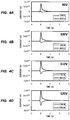
- FIGS. 2 A to 2 D , 3 A to 3 D , 4 A to 4 D , 5 A to 5 D , and 6 A to 6 D are graphs showing temporal changes in substrate current and electrode current when the applied voltage is 10 to 200 V. The value of the substrate current is multiplied by -1.
- the electrode current flows backward, but this is presumably because the electrons emitted from the trap level of the nitride semiconductor layer 12 are excessive to the electrons emitted from the trap level of the buffer layer 11 , so that a well is formed in the nitride semiconductor layer 12 and the potential of the nitride semiconductor layer 12 is increased so that electrons are supplied from the electrode 13.
- the density of electrical defects in the nitride semiconductor layer 12 made of, e.g., a GaN layer which is a part of the semiconductor layer is obtained.
- the density of electric charge emitted from a deep defect level can be obtained, it is also possible to obtain the electrical defect density of a wide bandgap semiconductor having a deep defect level.
- two types of electrical defect density evaluation methods will be described using this semiconductor element 1. In the following description, charge and electric capacity of each part are defined per unit area.
- the first method is a method of obtaining the density of the electrical defect of the semiconductor layer from the substrate current measured by the ammeter 15 a.
- ⁇ 0 is the dielectric constant of vacuum
- ⁇ G is the relative permittivity of the GaN layer 12
- ⁇ b is the relative permittivity of the buffer layer 11
- d G is the thickness of the GaN layer 12
- d b is the thickness of the buffer layer 11.
- ⁇ G and ⁇ b are 9.5 and 8.5 respectively, d G and d b are 1.3 ⁇ m and 3.5 ⁇ m, respectively, and the area of the electrode 13 corresponding to the area of the capacitor is 1 mm 2 .
- C cap is calculated to be 16 pF.
- Q cap is the accumulated charge when the semiconductor element 1 is an ideal capacitor in which all the regions of the buffer layer 11 and the GaN layer 12 (hereinafter referred to as epitaxial layer), and Q dep is the charge released from the epitaxial layer.
- Q cap can be obtained by integrating the substrate current I sub with the time ( 0 to 0 +) until the charge accumulates in the capacitor as shown in the following equation 3 , since the time until the charge accumulates in the capacitor is on the order of nanoseconds, the substrate current I sub which is enough for calculating Q cap cannot be measured under the usual measurement environment (the time resolution of the measuring apparatus is on the order of microseconds).
- Q cap ⁇ 0 0 + I sub dt
- Q cap is expressed by the product of C cap and the applied voltage V as in the following equation 4.
- C cap can be obtained from Equation 1 and is 16 pF for the semiconductor element 1. Therefore, for example, Q cap is obtained as 1.12 ⁇ 10 -9 C when the applied voltage V is 70 V. [Equation 4 ]
- Q cap C cap V
- Q dep when the applied voltage V of the semiconductor element 1 is 70 V can be obtained as 1.73 ⁇ 10 -10 C using the integrated value of the substrate current I sub up to 10 seconds.
- the substrate current I sub when the applied voltage V is 70 V is shown in FIG. 3 C .
- FIG. 7 is a graph obtained by plotting Q cap obtained from Equation 4 and Q total obtained from Equations 2 , 4 , and 5 for each applied voltage.
- the difference Q dep between Q total and Q cap at each applied voltage is caused by an increase in capacitance due to depletion of the epitaxial layer.
- the thickness z of the depletion layer is calculated. For example, it is calculated that z is 4.07 ⁇ m when the applied voltage V of the semiconductor element 1 is 70 V. In this case, since the thickness of the buffer layer 11 is 3.5 ⁇ m, the entire region of the buffer layer 11 is depleted, and the region of 0.57 ⁇ m thickness on the buffer layer 11 side of the GaN layer 12 is depleted.
- FIG. 8 is a graph showing the relationship between the applied voltage V and the thickness z of the depletion layer (at the position of the upper end of the depletion layer with reference to the interface between the substrate 10 and the buffer layer 11 ).
- the applied voltage V is 5 V, the entire region of the buffer layer 11 is depleted.
- Equation 9 is a formula showing the relationship between the electrical defect density ⁇ in the epitaxial layer in the steady state and the applied voltage V.
- x is a distance in the thickness direction with the interface between the substrate 10 and the buffer layer 11 as the origin
- ⁇ is a function of x.
- V q ⁇ z ⁇ 0 z ⁇ x ⁇ xdx
- Equation 12 it is possible to derive the electrical defect density ⁇ in the epitaxial layer at the position z (the distance from the interface between the substrate 10 and the buffer layer 11 ) with reference to the interface between the substrate 10 and the buffer layer 11.
- FIG. 9 is a graph showing the relationship between the electrical defect density ⁇ in the GaN layer 12 in the steady state obtained from Equation 12 and the position z.
- the maximum value of the electrical defect density of the GaN layer 12 which is obtained by using the charge amount immediately after the current application and the charge amount in the steady state as described above, is preferably 1.0 ⁇ 10 19 cm -3 or less, more preferably 2.0 ⁇ 10 18 cm -3 or less.
- an AlGaN layer is formed on the GaN layer 12 , and a region having a depth of several nm from the interface with the AlGaN layer of the GaN layer 12 serves as a current path.
- the second method is a method of obtaining the density of the electrical defect of the semiconductor layer from the difference between the substrate current measured by the ammeter 15 a and the electrode current measured by the ammeter 15 b.
- FIG. 10 is a graph showing the relationship between the net charge amount Q net accumulated in the epitaxial layer which is obtained by Equation 13 and the applied voltage V.
- the region where the net charge amount Q net decreases with the increase of the applied voltage V in FIG. 10 is the region where the electrode current flows backward.
- the net charge amount Q net is equal to the planar density (surface density) of the defects in the region where the net charge amount Q net decreases with the increase of the applied voltage V in FIG. 10 (the region where the applied voltage V is 20 V or less).
- the relationship between the net charge amount Q net and the applied voltage V in FIG. 10 can be converted into the relationship between the planar density of the defects and the position z.
- FIG. 11 is a graph showing the relationship between the planar density of electrical defects in the GaN layer 12 and the position z.
- the semiconductor element 1 having the structure shown in FIG. 1 was used as a sample of the electrical defect density evaluation method.
- the semiconductor element 1 has a substrate 10 made of Si having a ( 111 ) plane as a main surface, a GaN layer 12 formed on the substrate 10 via a buffer layer 11 , an electrode 13 having a Ti/Al/Ni/Au laminated structure.
- the GaN layer 12 has a C-GaN layer 12 a made of a GaN film doped with C (carbon) and an undoped GaN layer 12 b composed of a GaN film not doped with impurities on the C-GaN layer 12 a.
- the thicknesses of the buffer layer 11 , the C-GaN layer 12 a, and the undoped GaN layer 12 b were 3.5 ⁇ m, 730 nm, and 570 nm, respectively.
- the electrode 13 was a circular electrode having a radius of 560 ⁇ m and an area of 1 mm 2 .
- This electrical defect density is substantially equal to the electrical defect density obtained by the first method.
- the electrical defect density in the GaN layer 12 is obtained from the slope of the line in FIG. 11 . That is, by dividing the minute change amount of the planar density in a certain region in the GaN layer 12 by the minute change amount of the distance, the electrical defect density in that region can be obtained.
- the planar density of electrical defects increases with two gradients.
- the electrical defect density in the two regions where the slopes of increase of the planar density of this defects differ from each other is calculated as 3.7 ⁇ 10 14 cm -3 (in the region where the position z is approximately 3.5 to 3.8 ⁇ m) and 2.0 ⁇ 10 15 cm -3 (in the region where the position z is approximately 3.8 to 3.9 ⁇ m). It is considered that 3.7 ⁇ 10 14 cm -3 is equivalent to the electrical defect density obtained by the first method and indicates the electrical defect density in the region close to the buffer layer 11. Further, 2.0 ⁇ 10 15 cm -3 is considered to indicate the electrical defect density of the interface between the C-GaN layer 12 a and the undoped GaN layer 12 b or the undoped GaN layer 12 b.
- the method for evaluating the electrical defect density of a semiconductor in the above embodiment the density of the charge trapped in the deep defect level can be examined. Therefore, the method for evaluating the electrical defect density of a semiconductor in the above embodiment is particularly useful as a method for evaluating the electrical defect density of a wide bandgap semiconductor having a deep defect level, for example, a semiconductor layer having a bandgap of 2.5 eV or more.
- a highly reliable semiconductor device can be manufactured by using a semiconductor template including a semiconductor layer evaluated by the method for evaluating electrical defect density of a semiconductor in the above embodiment.
- it is useful for manufacturing a power device such as a power transistor using a wide bandgap semiconductor.
- the structure of the semiconductor element to be evaluated in the method for evaluating electrical defect density of a semiconductor layer according to the present invention is not limited to the structure of the semiconductor element 1.
- the substrate is not particularly limited as long as it is an electrically conductive substrate, and even when an insulating substrate is used, a semiconductor layer to be evaluated may be formed on the insulating substrate via an electrically conductive layer. In this case, instead of the substrate current, the current of the conductive layer on the insulating substrate is measured.
- the layer structure and composition of the semiconductor layer are also not particularly limited.
- the electrode is not particularly limited as long as it is an ohmic electrode.
- a method for evaluating the electrical defect density of a semiconductor layer applicable to a wide bandgap semiconductor having a deep defect level and a semiconductor element with a low electrical defect density which can be evaluated by the method are provided.
Landscapes
- Engineering & Computer Science (AREA)
- Manufacturing & Machinery (AREA)
- Physics & Mathematics (AREA)
- General Physics & Mathematics (AREA)
- Computer Hardware Design (AREA)
- Microelectronics & Electronic Packaging (AREA)
- Power Engineering (AREA)
- Testing Or Measuring Of Semiconductors Or The Like (AREA)
- Junction Field-Effect Transistors (AREA)
- Investigating Or Analyzing Materials By The Use Of Electric Means (AREA)
Abstract
Description
- The present invention relates to a method for evaluating the electrical defect density of a semiconductor layer and a semiconductor element.
- In a semiconductor element such as a transistor, if electrons or holes are trapped in a defect level (trap level) formed by impurities, defects, or the like in a semiconductor layer, generation of a leakage current or variation of a threshold voltage will be caused. Therefore, in order to manufacture a highly reliable semiconductor element, it is important to know the density of electrical defects (defects due to atomic defect or residual impurity) in the semiconductor layer. The density of the electrical defects is approximately equal to the sum of the carrier density and the density of the charge trapped in the defect level.
- Conventionally, there has been known a method for deriving a carrier density profile in a semiconductor layer from a CV curve (a curve showing the relationship between a capacitor capacitance and a gate voltage) profile (see, e.g., Non-Patent Literature 1).
- Non-Patent Literature 1: O. Ambacher, et al., "Two-dimensional electron gases induced by spontaneous and piezoelectric polarization charges in N- and Ga-face AlGaN/GaN heterostructures," Journal of Applied Physics 85, 3222, 1999.
- However, with the method for deriving the carrier density from the CV curve profile, it is difficult to monitor the density of electrons and holes trapped in a deep trap level. For this reason, it is difficult to evaluate the electrical defect density of a wide bandgap semiconductor having a deep trap level.
- It is an object of the present invention to provide a method for evaluating the electrical defect density of a semiconductor layer applicable to a wide bandgap semiconductor having a deep defect level and a semiconductor element having a low electrical defect density which can be evaluated by the method.
- One embodiment of the present invention provides a method for evaluating electrical defect density of a semiconductor layer of the following [1] to [3] and a semiconductor element of the following [4] to [6].
- [1] A method for evaluating an electrical defect density of a semiconductor layer, comprising:
- a step for measuring an electric current by applying a voltage to a semiconductor layer; and
- a step for deriving the electrical defect density in the semiconductor layer with use of a measured electric current value.
- [2] The method for evaluating an electrical defect density of a semiconductor layer according to [1] as above, wherein the electrical defect density in the semiconductor layer is derived using a value of a current on a low potential side of the semiconductor layer.
- [3] The method for evaluating an electrical defect density of a semiconductor layer according to [1] as above, wherein the electrical defect density in the semiconductor layer is derived by using a difference between a value of a current on a low potential side of the semiconductor layer and a value of a current on a high potential side of the semiconductor layer.
- [4] A semiconductor element, comprising:
a semiconductor layer serving as a current path, wherein a maximum value of an electrical defect density obtained by using a charge amount immediately after current application and a charge amount in steady state of the semiconductor layer is 1.0×1019 cm-3 or less. - [5] The semiconductor element, according to [4] as above, wherein a planar density of electrical defects in the semiconductor layer obtained by using a net charge amount accumulated in the semiconductor layer by the current application increases with two gradients, in a region where the planar density of the electrical defects increases as a distance from a low potential side surface at the time of the current application to the semiconductor layer.
- [6] The semiconductor element according to [4] or [5] as above, wherein a bandgap of the semiconductor layer is 2.5 eV or more.
- According to the present invention, it is possible to provide a method for evaluating the electrical defect density of a semiconductor layer, which can be applied to a wide bandgap semiconductor having a deep defect level, and a semiconductor element having a low electrical defect density which can be evaluated by the method.
-
-
FIG. 1 is a vertical sectional view of an example of a semiconductor element suitable for evaluation by the method for evaluating electrical defect density of a semiconductor layer according to this embodiment. -
FIG. 2A is a graph showing temporal changes in substrate current and electrode current when the applied voltage is 10V. -
FIG. 2B is a graph showing temporal changes in substrate current and electrode current when the applied voltage is 20V. -
FIG. 2C is a graph showing temporal changes in substrate current and electrode current when the applied voltage is 30V. -
FIG. 2D is a graph showing temporal changes in substrate current and electrode current when the applied voltage is 40V. -
FIG. 3A is a graph showing temporal changes in substrate current and electrode current when the applied voltage is 50V. -
FIG. 3B is a graph showing temporal changes in substrate current and electrode current when the applied voltage is 60V. -
FIG. 3C is a graph showing temporal changes in substrate current and electrode current when the applied voltage is 70V. -
FIG. 3D is a graph showing temporal changes in the substrate current and the electrode current when the applied voltage is 80V. -
FIG. 4A is a graph showing temporal changes in substrate current and electrode current when the applied voltage is 90V. -
FIG. 4B is a graph showing temporal changes in substrate current and electrode current when the applied voltage is 100V. -
FIG. 4C is a graph showing temporal changes in substrate current and electrode current when the applied voltage is 110V. -
FIG. 4D is a graph showing temporal changes in substrate current and electrode current when the applied voltage is 120V. -
FIG. 5A is a graph showing temporal changes in substrate current and electrode current when the applied voltage is 130V. -
FIG. 5B is a graph showing temporal changes in substrate current and electrode current when the applied voltage is 140V. -
FIG. 5C is a graph showing temporal changes in substrate current and electrode current when the applied voltage is 150V. -
FIG. 5D is a graph showing temporal changes in substrate current and the electrode current when the applied voltage is 160V. -
FIG. 6A is a graph showing temporal changes in substrate current and electrode current when the applied voltage is 170V. -
FIG. 6B is a graph showing temporal changes in substrate current and electrode current when the applied voltage is 180V. -
FIG. 6C is a graph showing temporal changes in substrate current and electrode current when the applied voltage is 190V. -
FIG. 6D is a graph showing temporal changes in substrate current and electrode current when the applied voltage is 200V. -
FIG. 7 is a graph plotting Qcap and QTOTAL for each applied voltage. -
FIG. 8 is a graph showing the relationship between the thickness z of the depletion layer and the applied voltage V. -
FIG. 9 is a graph showing the relationship between the electrical defect density ρ in the epitaxial layer in the steady state and the position z. -
FIG. 10 is a graph showing the relationship between the net charge amount Qnet accumulated in the epitaxial layer and the applied voltage V. -
FIG. 11 is a graph showing the relationship between the planar density of electrical defects in the GaN layer and the position z. -
FIG. 1 is a vertical cross-sectional view of asemiconductor element 1 which is an example of a semiconductor element suitable for evaluation by the method for evaluating electrical defect density of a semiconductor layer according to this embodiment. - The
semiconductor element 1 includes asubstrate 10 made of a semiconductor such as Si, anitride semiconductor layer 12 made of GaN or the like formed on thesubstrate 10 via abuffer layer 11, and anelectrode 13 having a laminated structure made of a plurality of metals such as Ti/Al/Ni/Au. Thenitride semiconductor layer 12 includes, e.g., an impurity-dopednitride semiconductor layer 12a made of a GaN film doped with impurities such as C (carbon) and an undopednitride semiconductor layer 12b made of a GaN film or the like which is undoped with impurities, on the impurity-dopednitride semiconductor layer 12a. - Although the materials and thicknesses of the
buffer layer 11, the impurity-dopednitride semiconductor layer 12a, and the undopednitride semiconductor layer 12b can be arbitrarily determined, in a method for evaluating an electrical defect density of a semiconductor described later, as an example, thenitride semiconductor layer 12, the impurity-dopednitride semiconductor layer 12a, and the undopednitride semiconductor layer 12b are aGaN layer 12, the C-GaN layer 12a, and anundoped GaN layer 12b, respectively. The thicknesses of thebuffer layer 11, the C-GaN layer 12a, and theundoped GaN layer 12b were 3.5 µm, 730 nm, and 570 nm, respectively. Also, theelectrode 13 may have an arbitrary shape, but similarly, as an example, a circular electrode having a radius of 560 µm and an area of 1 mm 2 was used. - A voltage can be applied between the
substrate 10 and theelectrode 13 by a variableDC power source 14. The current (substrate current) flowing through thesubstrate 10 can be measured by theammeter 15a and the current (electrode current) flowing through theelectrode 13 can be measured by theammeter 15b. -
FIGS. 2A to 2D ,3A to 3D ,4A to 4D ,5A to 5D , and6A to 6D are graphs showing temporal changes in substrate current and electrode current when the applied voltage is 10 to 200V. The value of the substrate current is multiplied by -1. - When the applied voltage is 90V or more, the electrode current flows backward, but this is presumably because the electrons emitted from the trap level of the
nitride semiconductor layer 12 are excessive to the electrons emitted from the trap level of thebuffer layer 11, so that a well is formed in thenitride semiconductor layer 12 and the potential of thenitride semiconductor layer 12 is increased so that electrons are supplied from theelectrode 13. - In the present embodiment, the density of electrical defects in the
nitride semiconductor layer 12 made of, e.g., a GaN layer which is a part of the semiconductor layer is obtained. According to the present embodiment, since the density of electric charge emitted from a deep defect level can be obtained, it is also possible to obtain the electrical defect density of a wide bandgap semiconductor having a deep defect level. Hereinafter, two types of electrical defect density evaluation methods will be described using thissemiconductor element 1. In the following description, charge and electric capacity of each part are defined per unit area. - The first method is a method of obtaining the density of the electrical defect of the semiconductor layer from the substrate current measured by the
ammeter 15a. - When the
semiconductor element 1 is regarded as a capacitor, the capacitance Ccap of thesemiconductor element 1, which is an ideal capacitor in which all regions of thebuffer layer 11 and theGaN layer 12 are depleted, is expressed by thefollowing equation 1.
[Equation 1]
- Here, ε 0 is the dielectric constant of vacuum, εG is the relative permittivity of the
GaN layer 12, εb is the relative permittivity of thebuffer layer 11, dG is the thickness of theGaN layer 12, and db is the thickness of thebuffer layer 11. As described above, the method for evaluating the electrical defect density of the semiconductor layer according to the present embodiment can also be applied to a semiconductor element including a plurality of semiconductor layers having different dielectric constants. - In the
semiconductor element 1, εG and εb are 9.5 and 8.5 respectively, dG and db are 1.3 µm and 3.5 µm, respectively, and the area of theelectrode 13 corresponding to the area of the capacitor is 1 mm 2 . As a result, Ccap is calculated to be 16 pF. - Further, the charge Qtotal accumulated in the depletion layers formed in the
buffer layer 11 and theGaN layer 12 is expressed by thefollowing equation 2.
[Equation 2]
- Here, Qcap is the accumulated charge when the
semiconductor element 1 is an ideal capacitor in which all the regions of thebuffer layer 11 and the GaN layer 12 (hereinafter referred to as epitaxial layer), and Qdep is the charge released from the epitaxial layer. - Among them, Qcap can be obtained by integrating the substrate current Isub with the time (0 to 0+) until the charge accumulates in the capacitor as shown in the
following equation 3, since the time until the charge accumulates in the capacitor is on the order of nanoseconds, the substrate current Isub which is enough for calculating Qcap cannot be measured under the usual measurement environment (the time resolution of the measuring apparatus is on the order of microseconds).
[Equation 3]
- On the other hand, Qcap is expressed by the product of Ccap and the applied voltage V as in the following equation 4. As described above, Ccap can be obtained from
Equation 1 and is 16 pF for thesemiconductor element 1. Therefore, for example, Qcap is obtained as 1.12 × 10⁻⁹ C when the applied voltage V is 70V.
[Equation 4]
- Qdep can be obtained by integrating the substrate current Isub with the time (0 + to ∞) after charge accumulation in the capacitor (steady state) as expressed by the following equation 5.
[Equation 5]
- From Equation 5, for example, Qdep when the applied voltage V of the
semiconductor element 1 is 70V can be obtained as 1.73 × 10⁻¹⁰ C using the integrated value of the substrate current Isub up to 10 seconds. The substrate current Isub when the applied voltage V is 70V is shown inFIG. 3C . - From Qcap obtained from Equation 4 and Qdep obtained from Equation 5, Qtotal is obtained using
Equation 2. -
FIG. 7 is a graph obtained by plotting Qcap obtained from Equation 4 and Qtotal obtained fromEquations 2, 4, and 5 for each applied voltage. The difference Qdep between Qtotal and Qcap at each applied voltage is caused by an increase in capacitance due to depletion of the epitaxial layer. - The electric capacity Cdep of the depletion layer in the steady state can be obtained using the following Equation 6.
[Equation 6]
- Also, when the thickness z of the depletion layer is larger than the thickness db of the
buffer layer 11, Cdep is expressed by the following Equation 7.
[Equation 7]
- From Equation 7, the thickness z of the depletion layer is calculated. For example, it is calculated that z is 4.07 µm when the applied voltage V of the
semiconductor element 1 is 70V. In this case, since the thickness of thebuffer layer 11 is 3.5 µm, the entire region of thebuffer layer 11 is depleted, and the region of 0.57 µm thickness on thebuffer layer 11 side of theGaN layer 12 is depleted. -
FIG. 8 is a graph showing the relationship between the applied voltage V and the thickness z of the depletion layer (at the position of the upper end of the depletion layer with reference to the interface between thesubstrate 10 and the buffer layer 11). When the applied voltage V is 5V, the entire region of thebuffer layer 11 is depleted. - When the relative permittivity εG of the
GaN layer 12 and the relative permittivity εb of thebuffer layer 11 can be regarded as being equal (εGε 0 = εbε 0 = ε), the above equations can be simplified. In this case, fromEquation 1 and Equation 4, Ccap and Qcap are expressed as ε/d and εV/d, respectively. FromEquations 2, 5, 6, and 7, Cdep is expressed as ε/z. As a result, the following Equation 8 is established.
[Equation 9]
- The following Equation 9 is a formula showing the relationship between the electrical defect density ρ in the epitaxial layer in the steady state and the applied voltage V. Here, x is a distance in the thickness direction with the interface between the
substrate 10 and thebuffer layer 11 as the origin, and ρ is a function of x.
[Equation 9]
- In Equation 9 and
Equations buffer layer 11 and theGaN layer 12, and is expressed as a function of the thickness z of the depletion layer. Equation 7 can be expressed using this ε as the followingEquation 10.
[Equation 10]
- The following
Equation 11 is derived from the first-order differentiation of Equation 9 with z.
[Equation 11]
- Then, the following
Equation 12 is obtained by modifyingEquation 10.
[Equation 12]
- From
Equation 12, it is possible to derive the electrical defect density ρ in the epitaxial layer at the position z (the distance from the interface between thesubstrate 10 and the buffer layer 11) with reference to the interface between thesubstrate 10 and thebuffer layer 11. -
FIG. 9 is a graph showing the relationship between the electrical defect density ρ in theGaN layer 12 in the steady state obtained fromEquation 12 and the position z. - For example, in the case where the
GaN layer 12 is used as a layer serving as a current path of a high electron mobility transistor (HEMT), the maximum value of the electrical defect density of theGaN layer 12, which is obtained by using the charge amount immediately after the current application and the charge amount in the steady state as described above, is preferably 1.0×1019 cm -3 or less, more preferably 2.0×1018 cm -3 or less. In the HEMT, an AlGaN layer is formed on theGaN layer 12, and a region having a depth of several nm from the interface with the AlGaN layer of theGaN layer 12 serves as a current path. - The second method is a method of obtaining the density of the electrical defect of the semiconductor layer from the difference between the substrate current measured by the
ammeter 15a and the electrode current measured by theammeter 15b. - The net charge amount Qnet accumulated in the epitaxial layer of the
semiconductor element 1 as a capacitor can be obtained by integrating the difference between the substrate current Isub and the electrode current Iele with time.
[Equation 13]
-
FIG. 10 is a graph showing the relationship between the net charge amount Qnet accumulated in the epitaxial layer which is obtained byEquation 13 and the applied voltage V. The region where the net charge amount Qnet decreases with the increase of the applied voltage V inFIG. 10 is the region where the electrode current flows backward. - It can be assumed that the net charge amount Qnet is equal to the planar density (surface density) of the defects in the region where the net charge amount Qnet decreases with the increase of the applied voltage V in
FIG. 10 (the region where the applied voltage V is 20V or less). Using the thickness z of the depletion layer at each voltage of the applied voltage V obtained by the first method, the relationship between the net charge amount Qnet and the applied voltage V inFIG. 10 can be converted into the relationship between the planar density of the defects and the position z. -
FIG. 11 is a graph showing the relationship between the planar density of electrical defects in theGaN layer 12 and the position z. - In the example, the
semiconductor element 1 having the structure shown inFIG. 1 was used as a sample of the electrical defect density evaluation method. Thesemiconductor element 1 has asubstrate 10 made of Si having a (111) plane as a main surface, aGaN layer 12 formed on thesubstrate 10 via abuffer layer 11, anelectrode 13 having a Ti/Al/Ni/Au laminated structure. TheGaN layer 12 has a C-GaN layer 12a made of a GaN film doped with C (carbon) and anundoped GaN layer 12b composed of a GaN film not doped with impurities on the C-GaN layer 12a. The thicknesses of thebuffer layer 11, the C-GaN layer 12a, and theundoped GaN layer 12b were 3.5 µm, 730 nm, and 570 nm, respectively. In addition, theelectrode 13 was a circular electrode having a radius of 560 µm and an area of 1 mm 2 . - The value of the intercept of
FIG. 11 , that is, the value of the planar density of the defects at the interface (z = 3.5 µm) between thebuffer layer 11 and theGaN layer 12 is 5.6×1010 cm-2 . Assuming that the defects are uniformly distributed in thebuffer layer 11 having a thickness of 3.5 µm, the electrical defect density in thebuffer layer 11 is calculated as 5.6×1010 cm -2 /3.5 µm = 1.4×1016 cm-3 . This electrical defect density is substantially equal to the electrical defect density obtained by the first method. - The electrical defect density in the
GaN layer 12 is obtained from the slope of the line inFIG. 11 . That is, by dividing the minute change amount of the planar density in a certain region in theGaN layer 12 by the minute change amount of the distance, the electrical defect density in that region can be obtained. - According to
FIG. 11 , in a region where the planar density of electrical defects increases (a region where the position z is about 3.5 to 3.9 µm) as a distance from the interface with thebuffer layer 11 which is the low potential side surface at the time of current application, the planar density of electrical defects increases with two gradients. - The electrical defect density in the two regions where the slopes of increase of the planar density of this defects differ from each other is calculated as 3.7×1014 cm -3 (in the region where the position z is approximately 3.5 to 3.8 µm) and 2.0×1015 cm -3 (in the region where the position z is approximately 3.8 to 3.9 µm). It is considered that 3.7×1014 cm -3 is equivalent to the electrical defect density obtained by the first method and indicates the electrical defect density in the region close to the
buffer layer 11. Further, 2.0×1015 cm -3 is considered to indicate the electrical defect density of the interface between the C-GaN layer 12a and theundoped GaN layer 12b or theundoped GaN layer 12b. - According to the method for evaluating the electrical defect density of a semiconductor in the above embodiment, the density of the charge trapped in the deep defect level can be examined. Therefore, the method for evaluating the electrical defect density of a semiconductor in the above embodiment is particularly useful as a method for evaluating the electrical defect density of a wide bandgap semiconductor having a deep defect level, for example, a semiconductor layer having a bandgap of 2.5 eV or more.
- A highly reliable semiconductor device can be manufactured by using a semiconductor template including a semiconductor layer evaluated by the method for evaluating electrical defect density of a semiconductor in the above embodiment. In particular, it is useful for manufacturing a power device such as a power transistor using a wide bandgap semiconductor.
- As described above, the structure of the semiconductor element to be evaluated in the method for evaluating electrical defect density of a semiconductor layer according to the present invention is not limited to the structure of the
semiconductor element 1. For example, the substrate is not particularly limited as long as it is an electrically conductive substrate, and even when an insulating substrate is used, a semiconductor layer to be evaluated may be formed on the insulating substrate via an electrically conductive layer. In this case, instead of the substrate current, the current of the conductive layer on the insulating substrate is measured. The layer structure and composition of the semiconductor layer are also not particularly limited. In addition, the electrode is not particularly limited as long as it is an ohmic electrode. - Although the embodiments of the present invention have been described above, the present invention is not limited to the above-described embodiments, and various modifications can be made without departing from the gist of the invention.
- In addition, the embodiment described above does not limit the invention according to the claims. It should also be noted that not all combinations of features described in the embodiments are indispensable to means for solving the problem of the invention.
- A method for evaluating the electrical defect density of a semiconductor layer applicable to a wide bandgap semiconductor having a deep defect level and a semiconductor element with a low electrical defect density which can be evaluated by the method are provided.
-
- 1
- Semiconductor element
- 10
- Substrate
- 11
- Buffer layer
- 12
- GaN layer
- 12a
- C-GaN layer
- 12b
- Undoped GaN layer
- 13
- Electrode
Claims (6)
- A method for evaluating an electrical defect density of a semiconductor layer, comprising:a step for measuring an electric current by applying a voltage to a semiconductor layer; anda step for deriving the electrical defect density in the semiconductor layer with use of a measured electric current value.
- The method for evaluating an electrical defect density of a semiconductor layer according to claim 1, wherein the electrical defect density in the semiconductor layer is derived using a value of a current on a low potential side of the semiconductor layer.
- The method for evaluating an electrical defect density of a semiconductor layer according to claim 1, wherein the electrical defect density in the semiconductor layer is derived by using a difference between a value of a current on a low potential side of the semiconductor layer and a value of a current on a high potential side of the semiconductor layer.
- A semiconductor element, comprising:
a semiconductor layer serving as a current path, wherein a maximum value of an electrical defect density obtained by using a charge amount immediately after current application and a charge amount in steady state of the semiconductor layer is 1.0×1019 cm -3 or less. - The semiconductor element, according to claim 4, wherein a planar density of electrical defects in the semiconductor layer obtained by using a net charge amount accumulated in the semiconductor layer by the current application increases with two gradients, in a region where the planar density of the electrical defects increases as a distance from a low potential side surface at the time of the current application to the semiconductor layer.
- The semiconductor element according to claim 4 or 5, wherein a bandgap of the semiconductor layer is 2.5 eV or more.
Applications Claiming Priority (2)
| Application Number | Priority Date | Filing Date | Title |
|---|---|---|---|
| JP2017161604A JP7220508B2 (en) | 2017-08-24 | 2017-08-24 | Method for evaluating electrical defect concentration in semiconductor layer |
| PCT/JP2018/029484 WO2019039257A1 (en) | 2017-08-24 | 2018-08-06 | Method for evaluating electrical defect density of semiconductor layer, and semiconductor element |
Publications (2)
| Publication Number | Publication Date |
|---|---|
| EP3675154A1 true EP3675154A1 (en) | 2020-07-01 |
| EP3675154A4 EP3675154A4 (en) | 2021-07-14 |
Family
ID=65438747
Family Applications (1)
| Application Number | Title | Priority Date | Filing Date |
|---|---|---|---|
| EP18847691.5A Pending EP3675154A4 (en) | 2017-08-24 | 2018-08-06 | Method for evaluating electrical defect density of semiconductor layer, and semiconductor element |
Country Status (6)
| Country | Link |
|---|---|
| US (1) | US11513149B2 (en) |
| EP (1) | EP3675154A4 (en) |
| JP (2) | JP7220508B2 (en) |
| CN (1) | CN111033711A (en) |
| TW (1) | TWI791592B (en) |
| WO (1) | WO2019039257A1 (en) |
Families Citing this family (1)
| Publication number | Priority date | Publication date | Assignee | Title |
|---|---|---|---|---|
| CN113203930B (en) * | 2021-04-23 | 2022-11-11 | 深圳市时代速信科技有限公司 | Schottky junction reliability assessment method and device |
Family Cites Families (8)
| Publication number | Priority date | Publication date | Assignee | Title |
|---|---|---|---|---|
| US6177292B1 (en) | 1996-12-05 | 2001-01-23 | Lg Electronics Inc. | Method for forming GaN semiconductor single crystal substrate and GaN diode with the substrate |
| JPH11126911A (en) * | 1997-10-24 | 1999-05-11 | Nippon Steel Corp | Pn junction diode and method for evaluating semiconductor substrate using the same |
| JPH11154696A (en) * | 1997-11-20 | 1999-06-08 | Nec Corp | Method of measuring mosfet capacitance |
| JP3251245B2 (en) * | 1998-06-10 | 2002-01-28 | 松下電器産業株式会社 | Method for evaluating semiconductor substrate and method for managing manufacturing process of semiconductor device |
| JP3269459B2 (en) | 1998-07-28 | 2002-03-25 | 日本電気株式会社 | MISFET overlap length measuring method, measuring device, and recording medium recording extraction program |
| JP2001196434A (en) * | 2000-01-06 | 2001-07-19 | Seiko Epson Corp | Method for evaluating transistor |
| JP2013074181A (en) * | 2011-09-28 | 2013-04-22 | Toyota Motor Corp | Semiconductor device and manufacturing method of the same |
| WO2013073623A1 (en) * | 2011-11-15 | 2013-05-23 | 富士電機株式会社 | Semiconductor device and method for manufacturing semiconductor device |
-
2017
- 2017-08-24 JP JP2017161604A patent/JP7220508B2/en active Active
-
2018
- 2018-08-06 EP EP18847691.5A patent/EP3675154A4/en active Pending
- 2018-08-06 WO PCT/JP2018/029484 patent/WO2019039257A1/en unknown
- 2018-08-06 CN CN201880054972.5A patent/CN111033711A/en active Pending
- 2018-08-06 US US16/639,040 patent/US11513149B2/en active Active
- 2018-08-16 TW TW107128599A patent/TWI791592B/en active
-
2023
- 2023-01-31 JP JP2023012882A patent/JP7441345B2/en active Active
Also Published As
| Publication number | Publication date |
|---|---|
| JP2023052789A (en) | 2023-04-12 |
| CN111033711A (en) | 2020-04-17 |
| TW201920971A (en) | 2019-06-01 |
| US11513149B2 (en) | 2022-11-29 |
| US20200225276A1 (en) | 2020-07-16 |
| TWI791592B (en) | 2023-02-11 |
| EP3675154A4 (en) | 2021-07-14 |
| JP7220508B2 (en) | 2023-02-10 |
| WO2019039257A1 (en) | 2019-02-28 |
| JP2019040988A (en) | 2019-03-14 |
| JP7441345B2 (en) | 2024-02-29 |
Similar Documents
| Publication | Publication Date | Title |
|---|---|---|
| Lagger et al. | Towards understanding the origin of threshold voltage instability of AlGaN/GaN MIS-HEMTs | |
| Ricco et al. | Oxide-thickness determination in thin-insulator MOS structures | |
| US11114296B2 (en) | Semiconductor wafer, electronic device, method of performing inspection on semiconductor wafer, and method of manufacturing electronic device | |
| Yeluri et al. | Interface states at the SiN/AlGaN interface on GaN heterojunctions for Ga and N-polar material | |
| DE102016216005B4 (en) | Method of evaluating a semiconductor device and apparatus for evaluating a semiconductor device | |
| Sun et al. | AC transconductance dispersion (ACGD): A method to profile oxide traps in MOSFETs without body contact | |
| Frigeri | An EBIC method for the quantitative determination of dopant concentration at striations in LEC GaAs | |
| JP7441345B2 (en) | semiconductor element | |
| Koester et al. | Length dependence of quantized conductance in ballistic constrictions fabricated on InAs/AlSb quantum wells | |
| Latrach et al. | Trap states analysis in AlGaN/AlN/GaN and InAlN/AlN/GaN high electron mobility transistors | |
| Wilson et al. | Recent Advancement in Charge-and Photo-Assisted Non-Contact Electrical Characterization of SiC, GaN, and AlGaN/GaN HEMT | |
| Zhang et al. | Direct determination of energy band alignments of Ni/Al 2 O 3/GaN MOS structures using internal photoemission spectroscopy | |
| Bera et al. | High frequency characterization and continuum modeling of ultrathin high-k (ZrO2) gate dielectrics on strained-Si | |
| Zubkov et al. | Voltage–capacitance and admittance investigations of electron states in self-organized InAs/GaAs quantum dots | |
| Yakovlev et al. | Investigation of delta-doped pHEMT InGaAs/GaAs/AlGaAs structures by the electrochemical capacitance-voltage technique | |
| Yakovlev et al. | Electrochemical capacitance-voltage profiling of nonuniformly doped GaAs heterostructures with SQWs and MQWs for LED applications | |
| Nanver et al. | Test structures without metal contacts for DC measurement of 2D-materials deposited on silicon | |
| Panepinto et al. | Temperature dependent EBIC and deep level transient spectroscopy investigation of different types of misfit-dislocations at MOVPE grown GaAs/InGaAs/GaAs-single-quantum wells | |
| Frolov et al. | Measurements of doping density in InAs by capacitance-voltage techniques with electrolyte barriers | |
| CN114300370A (en) | Depletion voltage acquisition method | |
| Nifa et al. | Novel CV measurements based method for the extraction of GaN buffer layer residual doping level in HEMT | |
| Findlay et al. | Recent Advancement in Charge and Photo-Assisted Non-Contact Electrical Characterization of SiC, GaN, and AlGaN/GaN HEMT | |
| Lorin et al. | Investigation of the role of back barrier depth and conductivity on the dynamic Ron and substrate ramping behavior of GaN Schottky diodes on silicon substrate | |
| Rivera et al. | Photocapacitance characteristics of (In, Ga) N/GaN MQW structures | |
| Kammeugne et al. | In Depth Parasitic Capacitance Analysis on GaN-HEMTs with Recessed MIS Gate |
Legal Events
| Date | Code | Title | Description |
|---|---|---|---|
| STAA | Information on the status of an ep patent application or granted ep patent |
Free format text: STATUS: THE INTERNATIONAL PUBLICATION HAS BEEN MADE |
|
| PUAI | Public reference made under article 153(3) epc to a published international application that has entered the european phase |
Free format text: ORIGINAL CODE: 0009012 |
|
| STAA | Information on the status of an ep patent application or granted ep patent |
Free format text: STATUS: REQUEST FOR EXAMINATION WAS MADE |
|
| 17P | Request for examination filed |
Effective date: 20200314 |
|
| AK | Designated contracting states |
Kind code of ref document: A1 Designated state(s): AL AT BE BG CH CY CZ DE DK EE ES FI FR GB GR HR HU IE IS IT LI LT LU LV MC MK MT NL NO PL PT RO RS SE SI SK SM TR |
|
| AX | Request for extension of the european patent |
Extension state: BA ME |
|
| DAV | Request for validation of the european patent (deleted) | ||
| DAX | Request for extension of the european patent (deleted) | ||
| RIC1 | Information provided on ipc code assigned before grant |
Ipc: H01L 21/66 20060101AFI20210324BHEP Ipc: H01L 29/20 20060101ALN20210324BHEP |
|
| A4 | Supplementary search report drawn up and despatched |
Effective date: 20210611 |
|
| RIC1 | Information provided on ipc code assigned before grant |
Ipc: H01L 21/66 20060101AFI20210607BHEP Ipc: H01L 29/20 20060101ALN20210607BHEP Ipc: H01L 29/207 20060101ALN20210607BHEP |