EP3672371B1 - Verfahren zur begrenzung der stromeinschaltung in kraftfahrzeugbeleuchtungsvorrichtungen - Google Patents
Verfahren zur begrenzung der stromeinschaltung in kraftfahrzeugbeleuchtungsvorrichtungen Download PDFInfo
- Publication number
- EP3672371B1 EP3672371B1 EP18215631.5A EP18215631A EP3672371B1 EP 3672371 B1 EP3672371 B1 EP 3672371B1 EP 18215631 A EP18215631 A EP 18215631A EP 3672371 B1 EP3672371 B1 EP 3672371B1
- Authority
- EP
- European Patent Office
- Prior art keywords
- input
- switching circuit
- control signal
- lighting device
- driver device
- Prior art date
- Legal status (The legal status is an assumption and is not a legal conclusion. Google has not performed a legal analysis and makes no representation as to the accuracy of the status listed.)
- Active
Links
Images
Classifications
-
- H—ELECTRICITY
- H05—ELECTRIC TECHNIQUES NOT OTHERWISE PROVIDED FOR
- H05B—ELECTRIC HEATING; ELECTRIC LIGHT SOURCES NOT OTHERWISE PROVIDED FOR; CIRCUIT ARRANGEMENTS FOR ELECTRIC LIGHT SOURCES, IN GENERAL
- H05B45/00—Circuit arrangements for operating light-emitting diodes [LED]
- H05B45/30—Driver circuits
- H05B45/37—Converter circuits
- H05B45/3725—Switched mode power supply [SMPS]
-
- H—ELECTRICITY
- H02—GENERATION; CONVERSION OR DISTRIBUTION OF ELECTRIC POWER
- H02M—APPARATUS FOR CONVERSION BETWEEN AC AND AC, BETWEEN AC AND DC, OR BETWEEN DC AND DC, AND FOR USE WITH MAINS OR SIMILAR POWER SUPPLY SYSTEMS; CONVERSION OF DC OR AC INPUT POWER INTO SURGE OUTPUT POWER; CONTROL OR REGULATION THEREOF
- H02M3/00—Conversion of DC power input into DC power output
- H02M3/02—Conversion of DC power input into DC power output without intermediate conversion into AC
- H02M3/04—Conversion of DC power input into DC power output without intermediate conversion into AC by static converters
- H02M3/10—Conversion of DC power input into DC power output without intermediate conversion into AC by static converters using discharge tubes with control electrode or semiconductor devices with control electrode
- H02M3/145—Conversion of DC power input into DC power output without intermediate conversion into AC by static converters using discharge tubes with control electrode or semiconductor devices with control electrode using devices of a triode or transistor type requiring continuous application of a control signal
- H02M3/155—Conversion of DC power input into DC power output without intermediate conversion into AC by static converters using discharge tubes with control electrode or semiconductor devices with control electrode using devices of a triode or transistor type requiring continuous application of a control signal using semiconductor devices only
-
- H—ELECTRICITY
- H02—GENERATION; CONVERSION OR DISTRIBUTION OF ELECTRIC POWER
- H02H—EMERGENCY PROTECTIVE CIRCUIT ARRANGEMENTS
- H02H9/00—Emergency protective circuit arrangements for limiting excess current or voltage without disconnection
- H02H9/001—Emergency protective circuit arrangements for limiting excess current or voltage without disconnection limiting speed of change of electric quantities, e.g. soft switching on or off
- H02H9/002—Emergency protective circuit arrangements for limiting excess current or voltage without disconnection limiting speed of change of electric quantities, e.g. soft switching on or off limiting inrush current on switching on of inductive loads subjected to remanence, e.g. transformers
-
- H—ELECTRICITY
- H02—GENERATION; CONVERSION OR DISTRIBUTION OF ELECTRIC POWER
- H02M—APPARATUS FOR CONVERSION BETWEEN AC AND AC, BETWEEN AC AND DC, OR BETWEEN DC AND DC, AND FOR USE WITH MAINS OR SIMILAR POWER SUPPLY SYSTEMS; CONVERSION OF DC OR AC INPUT POWER INTO SURGE OUTPUT POWER; CONTROL OR REGULATION THEREOF
- H02M3/00—Conversion of DC power input into DC power output
- H02M3/02—Conversion of DC power input into DC power output without intermediate conversion into AC
- H02M3/04—Conversion of DC power input into DC power output without intermediate conversion into AC by static converters
- H02M3/10—Conversion of DC power input into DC power output without intermediate conversion into AC by static converters using discharge tubes with control electrode or semiconductor devices with control electrode
- H02M3/145—Conversion of DC power input into DC power output without intermediate conversion into AC by static converters using discharge tubes with control electrode or semiconductor devices with control electrode using devices of a triode or transistor type requiring continuous application of a control signal
- H02M3/155—Conversion of DC power input into DC power output without intermediate conversion into AC by static converters using discharge tubes with control electrode or semiconductor devices with control electrode using devices of a triode or transistor type requiring continuous application of a control signal using semiconductor devices only
- H02M3/156—Conversion of DC power input into DC power output without intermediate conversion into AC by static converters using discharge tubes with control electrode or semiconductor devices with control electrode using devices of a triode or transistor type requiring continuous application of a control signal using semiconductor devices only with automatic control of output voltage or current, e.g. switching regulators
-
- H—ELECTRICITY
- H05—ELECTRIC TECHNIQUES NOT OTHERWISE PROVIDED FOR
- H05B—ELECTRIC HEATING; ELECTRIC LIGHT SOURCES NOT OTHERWISE PROVIDED FOR; CIRCUIT ARRANGEMENTS FOR ELECTRIC LIGHT SOURCES, IN GENERAL
- H05B45/00—Circuit arrangements for operating light-emitting diodes [LED]
- H05B45/30—Driver circuits
- H05B45/32—Pulse-control circuits
- H05B45/325—Pulse-width modulation [PWM]
-
- H—ELECTRICITY
- H05—ELECTRIC TECHNIQUES NOT OTHERWISE PROVIDED FOR
- H05B—ELECTRIC HEATING; ELECTRIC LIGHT SOURCES NOT OTHERWISE PROVIDED FOR; CIRCUIT ARRANGEMENTS FOR ELECTRIC LIGHT SOURCES, IN GENERAL
- H05B45/00—Circuit arrangements for operating light-emitting diodes [LED]
- H05B45/30—Driver circuits
- H05B45/37—Converter circuits
-
- H—ELECTRICITY
- H05—ELECTRIC TECHNIQUES NOT OTHERWISE PROVIDED FOR
- H05B—ELECTRIC HEATING; ELECTRIC LIGHT SOURCES NOT OTHERWISE PROVIDED FOR; CIRCUIT ARRANGEMENTS FOR ELECTRIC LIGHT SOURCES, IN GENERAL
- H05B45/00—Circuit arrangements for operating light-emitting diodes [LED]
- H05B45/50—Circuit arrangements for operating light-emitting diodes [LED] responsive to malfunctions or undesirable behaviour of LEDs; responsive to LED life; Protective circuits
-
- H—ELECTRICITY
- H02—GENERATION; CONVERSION OR DISTRIBUTION OF ELECTRIC POWER
- H02H—EMERGENCY PROTECTIVE CIRCUIT ARRANGEMENTS
- H02H9/00—Emergency protective circuit arrangements for limiting excess current or voltage without disconnection
- H02H9/001—Emergency protective circuit arrangements for limiting excess current or voltage without disconnection limiting speed of change of electric quantities, e.g. soft switching on or off
Definitions
- the invention lies in the field of driver devices for automotive lighting devices, and in particular for automotive lighting devices involving electroluminescent components, such as light emitting diodes, LEDs.
- LEDs are small components capable of producing beams having high luminosity at relatively low supply current intensities.
- interesting lighting contours may be designed, while at the same time both space and electrical power is saved, as compared to incandescent light sources.
- a voltage difference of a value equal or larger than a LED's forward voltage is applied to its two terminals, an electrical current flow through the LED and photons are emitted.
- the luminescence of a LED is an increasing function of the electrical current intensity that passes through it. As the luminescence is required to conform to predetermined regulations, it is important to carefully drive the intensity of the electrical current supplied to LEDs.
- driver devices for driving the power supply of a LED which generally use a DC/DC converter circuit to transform an electrical current having a first intensity, as supplied for example by an internal source of an automotive vehicle, such as a battery, into an electrical current having a second intensity, which is appropriate to power the LEDs.
- a current in-rush having an intensity that is larger than the average input current intensity is generally observed. This is due, for example but not only, to the capacitors in the converter circuit, which need to charge and which therefore draw a large electrical current initially.
- the in-rush current may translate may be falsely detected as an overload on the LED driver by the automotive vehicles body controller module. The latter may thus rais a false alert and disable the driver..
- US 2018/160515 A1 discloses a known control system comprising a control unit and a driver device of an automotive lighting device.
- the invention is defined by a control method according to claim 1 and by a control system according to claim 6. Further embodiments are set out in the dependent claims.
- the controlling step may comprise limiting the intensity of the electric current flowing through the first input to a predetermined value for a predetermined timespan.
- the controlling step may preferably comprise the cancellation of said limitation after said predetermined timespan has elapsed.
- the switching circuit may preferably be controlled to connect said first input to said lighting device.
- the switching circuit comprises a field effect transistor having a linear mode.
- the controlling step may further preferably comprise driving the transistor into linear mode using said control signal, so that the transistor acts as a resistance that limits the intensity of the electric current provided to the lighting device.
- the electronic components of said switching circuit may at least partly implement a reverse current protection circuit of said driver device.
- a computer program which, when run on a computer, leads the computer to realize the method steps in accordance with aspects of the invention.
- computer program product comprises a computer readable medium on which the computer program in accordance with an aspect of the invention is stored.
- a control system according to claim 6 is provided.
- the control unit may preferably comprise a microcontroller device operatively connected to said driver device.
- the driver device comprises a DC/DC converter.
- the converter may preferably comprise a switched mode converter circuit.
- the converter may preferably comprise a buck architecture, a boost architecture or a combined buck/boost architecture.
- the converter may be a Single Ended Primary Inductor Convertor, SEPIC.
- the driver control method in accordance with aspects of the invention, it becomes possible to limit the intensity of the in-rush current that arises when for example a LED driver is switched on, or when one among a plurality of available power inputs is connected to the driver.
- the in-rush current is smoothed by driving a switch that connects the driver to the power input first into a linear mode, wherein it acts basically like a resistance, before fully closing it. While in linear mode, the switch opposes itself to the flow of the in-rush current. As the in-rush current intensity is limited, a false overload detection is avoided.
- Field effect transistors are often used as power switched in reverse current protection circuits for LED drivers.
- the method in accordance with aspects of the invention may be advantageously implemented by using these existing hardware components instead of requiring the addition of further hardware components. Indeed, a MOSFET power switch may be driven into linear mode for a small time, by applying the appropriate control signal to its gate terminal.
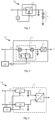
- FIG. 1 illustrates a control system 100 that includes a driver device 110 of an automotive lighting device 10.
- the lighting device is schematically illustrated as comprising a series string of light emitting diodes, LED, but the invention is not limited to this example.
- the driver device is suitable for supplying electricity to the lighting device and comprises electronic circuitry to that effect.
- the driver device comprises means for receiving a first input 112.
- the first input 112 is an electricity supply, as provided for example by an electricity source that is internal to the automotive vehicle, such as a battery.
- the driver device further comprises a switching circuit 114 for selectively connecting said first input to the lighting device and for selectively limiting the intensity of the electric current flowing through the first input.
- a second input 116 for receiving a control signal for the switching circuit is provided.
- the driver device may further comprise other non-illustrated circuitry, for example a known converter circuit.
- the control method of the switching circuit is implemented by a controlling unit 120, which may for example be implemented using a microcontroller device programmed to that effect.
- the controlling unit 120 generates on one of its outputs, functionally connected to the switching circuit 114, a control signal that carries the controls addressed to the switching circuit.
- the control method comprises the steps of
- the predetermined value is a current threshold which may be implemented by various electrical components of the switching circuit. Typically, the limitation is active for about 1 to 2 milliseconds, after which the in-rush phenomenon is generally no longer noticeable. The limitation may as well be active for a shorter or longer period. Past this predetermined time, the control signal 116 closes the switching circuit completely without limiting the supplied current intensity.
- FIG. 2 illustrates the inventive power supply system 200 for implementing a preferred embodiment of the method in accordance with aspects of the invention.
- the system 200 includes a driver device 210 of an automotive lighting device 10.
- the driver device is suitable for supplying electricity to the lighting device and comprises electronic circuitry to that effect.
- the driver device comprises means for receiving a first input 212.
- the first input 212 is an electricity supply, as provided for example by an electricity source that is internal to the automotive vehicle, such as a battery.
- the driver device further comprises a switching circuit 214 for selectively connecting said first input to the lighting device and for selectively limiting the intensity of the electric current provided to the lighting device.
- a second input 216 for receiving a control signal for the switching circuit is provided.
- the driver device may further comprise other circuitry, for example a known converter circuit 215.
- the converter circuit 215 converts the input current into a charge current of appropriate intensity for powering the lighting device.
- the converter circuit may for example comprise a buck converter for lowering the power, a boost converter for raising the power, or a combined boost/buck architecture. It is for example known in the art to use switched mode converter circuits such as a single ended primary inductor converter, SEPIC. In such converters, the performance of the converter is controlled using a switching signal that is not illustrated in the context of the present invention. The switching signal is applied to a control switch of the converter circuit, thereby defining its duty cycle.
- SEPIC single ended primary inductor converter
- the control method of the switching circuit 214 is implemented by a controlling unit 220, which may for example be implemented using a microcontroller device programmed to that effect.
- the controlling unit 220 generates on one of its outputs, functionally connected to the switching circuit 214 through resistance R1, a control signal 216 that carries the controls addressed to the switching circuit.
- the control method comprises the steps of:
- the switching circuit 214 shown in Figure 2 is also used to implement a reverse current protection for the converter circuit 215.
- the state of the MOSFET transistors Q1 and Q2 is driven by control signal 216 through the circuit implemented by the Zener diode D1, the capacitor C1 and the resistance R2.
- the control signal 216 is a pulse width modulated PWM signal, which is a binary periodic signal having an ON state and an OFF state, and which is characterized by its duty cycle, i.e. the ratio between the duration of the ON state and the total period duration.
- the PWM signal is suitable for driving the power switch Q1 selectively into either closed, open or linear mode, as required by the method in accordance with aspects of the invention.
- Applying the PWM signal to the capacitor C1, one terminal of which is connected to the gate of Q1, further helps to filter and smooth the current in-rush that is detected on input 212.
- the example 300 shown in Figure 3 comprises a driver device 310 in which a single converter circuit 315 is shared in time by a plurality of lighting functions, wherein each lighting function may require one of a plurality of available power inputs 312, 312', of which two are illustrated, without limiting the invention to the number of two.
- Each power supply input 312, 312' is associated with a dedicated switching circuit 314, 314', of which each one is akin to the switching circuits described in previous embodiments.
- the switching circuits are controlled by respective control signals 316, 316', which are generated in this example by the common controlling unit 320, and which implement the same functionality that has been described for the control signals 116, 216 in the context of the previous embodiments.
- separate controlling units may as well be used for generating the plurality of control signals.
- Time shared converters are for example used in automotive lighting device.
- a turn indicator, TI, and parking light, PL, function are both requested by the car, the converter supplies both the TI and PL LEDs using a time-sharing schedule and using the same input power supply, for example 312.
- input supply 312' must be used to supply power to the PL alone due to practical and regulation constraints.
- power is detected on input supply 312, which is then used to replace input 312'. There is thus a periodic switching between power supply inputs 312 and 312', which is implemented by controlling the switching circuits 314, 314' accordingly.
- the corresponding switching circuits 314, 314' go into their closed mode, they are driven for 1-2 ms into a linear mode using control signals 316 and 316' respectively, in which they act as a resistance in order to smooth the current in-rush that is otherwise fed forward to the converter circuit 315.
- the proposed method avoids the periodic in-rushes at the converter circuits input, which would otherwise be detected erroneously as driver failure due to input overload.
Landscapes
- Engineering & Computer Science (AREA)
- Power Engineering (AREA)
- Lighting Device Outwards From Vehicle And Optical Signal (AREA)
- Circuit Arrangement For Electric Light Sources In General (AREA)
Claims (7)
- Steuerverfahren für eine Treibervorrichtung (210, 310) einer Kraftfahrzeugbeleuchtungsvorrichtung (10), wobei die Treibervorrichtung geeignet ist zum Zuführen von Elektrizität zu der Kraftfahrzeugbeleuchtungsvorrichtung und einen ersten Eingang (212, 312, 312') zum Empfangen einer Elektrizitätsversorgung, eine Umschaltschaltung (214, 314, 3140) zum selektiven Verbinden des ersten Eingangs mit der Kraftfahrzeugbeleuchtungsvorrichtung und zum selektiven Begrenzen der Intensität des der Kraftfahrzeugbeleuchtungsvorrichtung bereitgestellten elektrischen Stroms, und einen zweiten Eingang (216, 316, 316') zum Empfangen eines Steuersignals für die Umschaltschaltung umfasst, wobei das Steuersignal ein Pulsbreitenmodulations- bzw. PWM-Signal ist und wobei das Verfahren die folgenden Schritte umfasst:- Detektieren des Vorliegens einer Elektrizitätsversorgung an dem ersten Eingang unter Verwendung einer Detektionsschaltung;- nach der Detektion, Steuern der Umschaltschaltung (214, 314, 314') unter Verwendung des Steuersignals (216, 316, 316'), sodass der erste Eingang (212, 312, 312') mit der Beleuchtungsvorrichtung verbunden wird und sodass die Intensität des durch den ersten Eingang fließenden elektrischen Stroms auf einen vorbestimmten Wert begrenzt wird,wobei die Treibervorrichtung (210, 310) einen DC/DC-Wandler (215, 315) umfasst, der einen Eingang und einen Ausgang umfasst, wobei der DC/DC-Wandler einen Eingang umfasst, der über einen ersten Kondensator mit Masse verbunden ist, wobei die Umschaltschaltung einen Ausgang umfasst, der mit dem Eingang des DC/DC-Wandlers verbunden ist, wobei die Umschaltschaltung Folgendes umfasst:- einen Elektrizitätsversorgungseingang, der mit dem ersten Eingang (212, 312, 312') der Treibervorrichtung verbunden ist,- einen Steuersignaleingang, der mit dem zweiten Eingang der Treibervorrichtung verbunden ist, zum Empfangen des Steuersignals (216, 316, 316'),dadurch gekennzeichnet, dass das Verfahren ferner Anlegen des Steuersignals an den Steuersignaleingang umfasst, wobei die Umschaltschaltung ferner Folgendes umfasst:- eine Zener-Diode (D1) mit einer Anode und einer Kathode,- einen zweiten Kondensator (C1) mit einem ersten und einem zweiten Kondensatoranschluss,- einen Widerstand (R2) mit einem ersten und einem zweiten Widerstandsanschluss,- einen ersten Leistungsschalter (Q1) und einen zweiten Leistungsschalter (Q2), wobei es sich bei den Schaltern um Leistungstransistoren des P-Kanal-Anreicherungsmodus-MOSFET-Typs handelt, die jeweils ein erstes und ein zweites Gate, eine erste und eine zweite Source und einen ersten und einen zweiten Drain umfassen,- wobei der Steuersignaleingang durch einen einzelnen ersten Knoten mit dem ersten Gate, dem zweiten Gate, der Anode, dem ersten Widerstandsanschluss und dem ersten Kondensatoranschluss verbunden ist,- wobei die erste Source, die zweite Source, die Kathode, der zweite Kondensatoranschluss und der zweite Widerstandsanschluss in einem zweiten Knoten miteinander verbunden sind,- wobei der erste Drain mit dem Elektrizitätsversorgungseingang verbunden ist,- wobei der zweite Drain mit dem Ausgang der Umschaltschaltung verbunden ist.
- Verfahren nach Anspruch 1, wobei der Schritt des Steuerns der Umschaltschaltung unter Verwendung des Steuersignals nach der Detektion Begrenzen der Intensität des durch den ersten Eingang fließenden elektrischen Stroms auf einen vorbestimmten Wert für eine vorbestimmte Zeitspanne umfasst.
- Verfahren nach Anspruch 2, wobei der der Schritt des Steuerns der Umschaltschaltung unter Verwendung des Steuersignals die Aufhebung der Begrenzung nach Ablauf der vorbestimmten Zeitspanne umfasst.
- Verfahren nach einem der vorhergehenden Ansprüche, wobei der erste Leistungsschalter (Q1) einen linearen Modus aufweist und wobei der Steuerschritt nach der Detektion Ansteuern des ersten Leistungsschalters (Q1) in den linearen Modus unter Verwendung des Steuersignals (216) umfasst, sodass der Transistor als Widerstand wirkt, der die Intensität des der Beleuchtungsvorrichtung bereitgestellten elektrischen Stroms begrenzt.
- Verfahren nach einem der vorhergehenden Ansprüche, wobei das Verfahren ferner Implementieren einer Rückstromschutzschaltung der Treibervorrichtung (210) durch die Umschaltschaltung (214) umfasst.
- Steuersystem (200, 300), umfassend eine Steuereinheit (220, 320) und eine Treibervorrichtung (210, 310) einer Kraftfahrzeugbeleuchtungsvorrichtung (10), wobei die Treibervorrichtung geeignet ist zum Zuführen von Elektrizität zu der Kraftfahrzeugbeleuchtungsvorrichtung und einen ersten Eingang (212, 312, 312') zum Empfangen einer Elektrizitätsversorgung, eine Umschaltschaltung (214, 314, 314') zum selektiven Verbinden des ersten Eingangs mit der Kraftfahrzeugbeleuchtungsvorrichtung und zum selektiven Begrenzen der Intensität des der Kraftfahrzeugbeleuchtungsvorrichtung bereitgestellten elektrischen Stroms, und einen zweiten Eingang (216, 316, 316') zum Empfangen eines Steuersignals für die Umschaltschaltung umfasst, wobei das Steuersignal ein Pulsbreitenmodulations- bzw. PWM-Signal ist und wobei das Verfahren die folgenden Schritte umfasst:- eine Detektionsschaltung zum Detektieren des Vorliegens einer Elektrizitätsversorgung an dem ersten Eingang;- einen Steuersignalgenerator, der ausgelegt ist zum Erzeugen des Steuersignals zum Steuern der Umschaltschaltung nach der Detektion, sodass der erste Eingang mit der Kraftfahrzeugbeleuchtungsvorrichtung verbunden wird und sodass die Intensität des durch den ersten Eingang fließenden elektrischen Stroms auf einen vorbestimmten Wert begrenzt wird; undwobei die Treibervorrichtung (210, 310) einen DC/DC-Wandler (215, 315) umfasst, der einen Eingang und einen Ausgang umfasst, wobei der DC/DC-Wandler einen Eingang umfasst, der über einen ersten Kondensator mit Masse verbunden ist, wobei die Umschaltschaltung einen Ausgang umfasst, der mit dem Eingang des DC/DC-Wandlers verbunden ist, wobei die Umschaltschaltung Folgendes umfasst:- einen Elektrizitätsversorgungseingang, der mit dem ersten Eingang (212, 312, 312`) der Treibervorrichtung verbunden ist,- einen Steuersignaleingang, der mit dem zweiten Eingang der Treibervorrichtung verbunden ist, zum Empfangen des Steuersignals (216, 316, 316'),dadurch gekennzeichnet, dass die Umschaltschaltung ferner Folgendes umfasst:- eine Zener-Diode (D1) mit einer Anode und einer Kathode,- einen zweiten Kondensator (C1) mit einem ersten und einem zweiten Kondensatoranschluss,- einen Widerstand (R2) mit einem ersten und einem zweiten Widerstandsanschluss,- einen ersten Leistungsschalter (Q1) und einen zweiten Leistungsschalter (Q2), wobei es sich bei den Schaltern um Leistungstransistoren des P-Kanal-Anreicherungsmodus-MOSFET-Typs handelt, die jeweils ein erstes und ein zweites Gate, eine erste und eine zweite Source und einen ersten und einen zweiten Drain umfassen,- wobei der Steuersignaleingang durch einen einzelnen ersten Knoten mit dem ersten Gate, dem zweiten Gate, der Anode, dem ersten Widerstandsanschluss und dem ersten Kondensatoranschluss verbunden ist,- wobei die erste Source, die zweite Source, die Kathode, der zweite Kondensatoranschluss und der zweite Widerstandsanschluss in einem zweiten Knoten miteinander verbunden sind,- wobei der erste Drain mit dem Elektrizitätsversorgungseingang verbunden ist,- wobei der zweite Drain mit dem Ausgang der Umschaltschaltung verbunden ist.
- Steuersystem nach Anspruch 6, wobei die Steuerungseinheit (220, 320) eine Mikrocontrollervorrichtung umfasst, die mit der Treibervorrichtung (210, 310) wirkverbunden ist.
Priority Applications (4)
| Application Number | Priority Date | Filing Date | Title |
|---|---|---|---|
| EP18215631.5A EP3672371B1 (de) | 2018-12-21 | 2018-12-21 | Verfahren zur begrenzung der stromeinschaltung in kraftfahrzeugbeleuchtungsvorrichtungen |
| US17/416,275 US11570864B2 (en) | 2018-12-21 | 2019-12-05 | Method for limiting current in-rush in automotive lighting devices |
| PCT/EP2019/083852 WO2020126522A1 (en) | 2018-12-21 | 2019-12-05 | Method for limiting current in-rush in automotive lighting devices |
| CN201980085291.XA CN113243143B (zh) | 2018-12-21 | 2019-12-05 | 用于限制汽车照明装置中的电流浪涌的方法 |
Applications Claiming Priority (1)
| Application Number | Priority Date | Filing Date | Title |
|---|---|---|---|
| EP18215631.5A EP3672371B1 (de) | 2018-12-21 | 2018-12-21 | Verfahren zur begrenzung der stromeinschaltung in kraftfahrzeugbeleuchtungsvorrichtungen |
Publications (2)
| Publication Number | Publication Date |
|---|---|
| EP3672371A1 EP3672371A1 (de) | 2020-06-24 |
| EP3672371B1 true EP3672371B1 (de) | 2024-03-20 |
Family
ID=65019267
Family Applications (1)
| Application Number | Title | Priority Date | Filing Date |
|---|---|---|---|
| EP18215631.5A Active EP3672371B1 (de) | 2018-12-21 | 2018-12-21 | Verfahren zur begrenzung der stromeinschaltung in kraftfahrzeugbeleuchtungsvorrichtungen |
Country Status (4)
| Country | Link |
|---|---|
| US (1) | US11570864B2 (de) |
| EP (1) | EP3672371B1 (de) |
| CN (1) | CN113243143B (de) |
| WO (1) | WO2020126522A1 (de) |
Citations (1)
| Publication number | Priority date | Publication date | Assignee | Title |
|---|---|---|---|---|
| US5811948A (en) * | 1995-08-02 | 1998-09-22 | Nippondenso Co., Ltd. | Control apparatus for electric motor |
Family Cites Families (12)
| Publication number | Priority date | Publication date | Assignee | Title |
|---|---|---|---|---|
| JP3842061B2 (ja) * | 2001-03-26 | 2006-11-08 | 矢崎総業株式会社 | 負荷駆動装置 |
| US8053923B2 (en) * | 2005-12-12 | 2011-11-08 | Mitsubishi Electric Corporation | Light-emitting diode lighting apparatus and vehicle light lighting apparatus using the same |
| CN102801293A (zh) * | 2011-05-23 | 2012-11-28 | 上海航天测控通信研究所 | 一种抑制开机浪涌电流的保护装置 |
| JP5942257B2 (ja) * | 2012-06-08 | 2016-06-29 | パナソニックIpマネジメント株式会社 | 点灯装置および前照灯、車両 |
| CN103826375B (zh) * | 2012-11-16 | 2016-02-10 | 台达电子工业股份有限公司 | 具即时改善电流尖峰因数功能的电子安定器 |
| JP6103348B2 (ja) * | 2012-12-07 | 2017-03-29 | 東芝ライテック株式会社 | 電源回路及び照明装置 |
| JP6491414B2 (ja) * | 2014-02-10 | 2019-03-27 | 新電元工業株式会社 | 車両用ランプ駆動装置及び車両用ランプ駆動方法 |
| JP6418443B2 (ja) * | 2014-09-10 | 2018-11-07 | パナソニックIpマネジメント株式会社 | 点灯装置、照明装置および車両 |
| CN108650747B (zh) * | 2014-09-16 | 2020-11-10 | 株式会社小糸制作所 | 点灯电路及使用该点灯电路的车辆用灯具 |
| TWI620404B (zh) * | 2015-06-05 | 2018-04-01 | 宸定科技股份有限公司 | 一種可應用於外接式硬碟之電源轉換電路 |
| US9985429B2 (en) * | 2016-09-21 | 2018-05-29 | Express Imaging Systems, Llc | Inrush current limiter circuit |
| DE102017214056B3 (de) * | 2017-08-11 | 2018-10-18 | Continental Automotive Gmbh | Treiberschaltung für eine Leuchtdiodenanordnung sowie Leuchtvorrichtung und Kraftfahrzeug |
-
2018
- 2018-12-21 EP EP18215631.5A patent/EP3672371B1/de active Active
-
2019
- 2019-12-05 CN CN201980085291.XA patent/CN113243143B/zh active Active
- 2019-12-05 WO PCT/EP2019/083852 patent/WO2020126522A1/en not_active Ceased
- 2019-12-05 US US17/416,275 patent/US11570864B2/en active Active
Patent Citations (1)
| Publication number | Priority date | Publication date | Assignee | Title |
|---|---|---|---|---|
| US5811948A (en) * | 1995-08-02 | 1998-09-22 | Nippondenso Co., Ltd. | Control apparatus for electric motor |
Also Published As
| Publication number | Publication date |
|---|---|
| US11570864B2 (en) | 2023-01-31 |
| CN113243143B (zh) | 2024-05-07 |
| WO2020126522A1 (en) | 2020-06-25 |
| US20220053620A1 (en) | 2022-02-17 |
| CN113243143A (zh) | 2021-08-10 |
| EP3672371A1 (de) | 2020-06-24 |
Similar Documents
| Publication | Publication Date | Title |
|---|---|---|
| US8970136B2 (en) | Semiconductor light source lighting circuit and vehicular lamp | |
| CN105472834B (zh) | 点灯电路及使用该点灯电路的车辆用灯具 | |
| US9992835B2 (en) | Lighting circuit | |
| US7741788B2 (en) | Light emitting apparatus with current limiting | |
| US9386646B2 (en) | Vehicle lamp and vehicle lamp driving device | |
| CN107148105B (zh) | 用于机动车辆的照明装置的包括多个输出的电源 | |
| US9623791B2 (en) | Lighting device, vehicle illumination device, and vehicle | |
| JP6591814B2 (ja) | 点灯回路およびそれを用いた車両用灯具 | |
| US20150069906A1 (en) | Circuit arrangement, lighting unit for a vehicle and method for driving semiconductor lighting elements | |
| US9986611B2 (en) | Light-emitting element driving device, light-emitting device, and vehicle | |
| US10143055B2 (en) | Illuminating device for vehicles | |
| US9992826B1 (en) | Dual mode constant current LED driver | |
| JP2014050112A (ja) | 直流電源回路およびled点灯回路 | |
| CN114747297A (zh) | 发光控制系统、发光系统、发光控制装置以及发光装置 | |
| US12004275B2 (en) | Controlling light emitting diodes for switching patterns | |
| US11570864B2 (en) | Method for limiting current in-rush in automotive lighting devices | |
| JP2014157785A (ja) | 駆動回路、車輌用灯具 | |
| CN111316548B (zh) | 点灯电路以及车辆用灯具 | |
| JP2021002440A (ja) | 点灯制御装置、点灯制御方法、車両用灯具 | |
| US11490486B2 (en) | Method for maintaining luminosity when switching input power in automotive lighting devices | |
| KR102050367B1 (ko) | 차량용 램프 회로 토폴리지 | |
| CN110651421B (zh) | 具有可选输出电压范围的转换器 | |
| US11987178B2 (en) | Light assembly with a fail safe mode for a low beam function | |
| US10433395B2 (en) | Device for driving the electrical power supply of light sources of an automotive vehicle |
Legal Events
| Date | Code | Title | Description |
|---|---|---|---|
| PUAI | Public reference made under article 153(3) epc to a published international application that has entered the european phase |
Free format text: ORIGINAL CODE: 0009012 |
|
| STAA | Information on the status of an ep patent application or granted ep patent |
Free format text: STATUS: REQUEST FOR EXAMINATION WAS MADE |
|
| 17P | Request for examination filed |
Effective date: 20181221 |
|
| AK | Designated contracting states |
Kind code of ref document: A1 Designated state(s): AL AT BE BG CH CY CZ DE DK EE ES FI FR GB GR HR HU IE IS IT LI LT LU LV MC MK MT NL NO PL PT RO RS SE SI SK SM TR |
|
| AX | Request for extension of the european patent |
Extension state: BA ME |
|
| STAA | Information on the status of an ep patent application or granted ep patent |
Free format text: STATUS: EXAMINATION IS IN PROGRESS |
|
| 17Q | First examination report despatched |
Effective date: 20210514 |
|
| REG | Reference to a national code |
Ref country code: DE Ref legal event code: R079 Free format text: PREVIOUS MAIN CLASS: H05B0033080000 Ipc: H05B0045370000 Ref document number: 602018066812 Country of ref document: DE |
|
| RIC1 | Information provided on ipc code assigned before grant |
Ipc: H05B 45/37 20200101AFI20221207BHEP |
|
| P01 | Opt-out of the competence of the unified patent court (upc) registered |
Effective date: 20230528 |
|
| REG | Reference to a national code |
Ref country code: DE Free format text: PREVIOUS MAIN CLASS: H05B0045370000 Ref country code: DE Ref legal event code: R079 Ref document number: 602018066812 Country of ref document: DE Free format text: PREVIOUS MAIN CLASS: H05B0045370000 Ipc: H05B0045500000 |
|
| GRAP | Despatch of communication of intention to grant a patent |
Free format text: ORIGINAL CODE: EPIDOSNIGR1 |
|
| STAA | Information on the status of an ep patent application or granted ep patent |
Free format text: STATUS: GRANT OF PATENT IS INTENDED |
|
| RIC1 | Information provided on ipc code assigned before grant |
Ipc: H02M 3/155 20060101ALI20230919BHEP Ipc: H05B 45/37 20200101ALI20230919BHEP Ipc: H05B 45/50 20200101AFI20230919BHEP |
|
| INTG | Intention to grant announced |
Effective date: 20231009 |
|
| GRAS | Grant fee paid |
Free format text: ORIGINAL CODE: EPIDOSNIGR3 |
|
| GRAA | (expected) grant |
Free format text: ORIGINAL CODE: 0009210 |
|
| STAA | Information on the status of an ep patent application or granted ep patent |
Free format text: STATUS: THE PATENT HAS BEEN GRANTED |
|
| AK | Designated contracting states |
Kind code of ref document: B1 Designated state(s): AL AT BE BG CH CY CZ DE DK EE ES FI FR GB GR HR HU IE IS IT LI LT LU LV MC MK MT NL NO PL PT RO RS SE SI SK SM TR |
|
| REG | Reference to a national code |
Ref country code: GB Ref legal event code: FG4D |
|
| REG | Reference to a national code |
Ref country code: CH Ref legal event code: EP |
|
| REG | Reference to a national code |
Ref country code: DE Ref legal event code: R096 Ref document number: 602018066812 Country of ref document: DE |
|
| REG | Reference to a national code |
Ref country code: IE Ref legal event code: FG4D |
|
| PG25 | Lapsed in a contracting state [announced via postgrant information from national office to epo] |
Ref country code: LT Free format text: LAPSE BECAUSE OF FAILURE TO SUBMIT A TRANSLATION OF THE DESCRIPTION OR TO PAY THE FEE WITHIN THE PRESCRIBED TIME-LIMIT Effective date: 20240320 |
|
| REG | Reference to a national code |
Ref country code: LT Ref legal event code: MG9D |
|
| PG25 | Lapsed in a contracting state [announced via postgrant information from national office to epo] |
Ref country code: GR Free format text: LAPSE BECAUSE OF FAILURE TO SUBMIT A TRANSLATION OF THE DESCRIPTION OR TO PAY THE FEE WITHIN THE PRESCRIBED TIME-LIMIT Effective date: 20240621 |
|
| PG25 | Lapsed in a contracting state [announced via postgrant information from national office to epo] |
Ref country code: HR Free format text: LAPSE BECAUSE OF FAILURE TO SUBMIT A TRANSLATION OF THE DESCRIPTION OR TO PAY THE FEE WITHIN THE PRESCRIBED TIME-LIMIT Effective date: 20240320 Ref country code: RS Free format text: LAPSE BECAUSE OF FAILURE TO SUBMIT A TRANSLATION OF THE DESCRIPTION OR TO PAY THE FEE WITHIN THE PRESCRIBED TIME-LIMIT Effective date: 20240620 |
|
| REG | Reference to a national code |
Ref country code: NL Ref legal event code: MP Effective date: 20240320 |
|
| PG25 | Lapsed in a contracting state [announced via postgrant information from national office to epo] |
Ref country code: RS Free format text: LAPSE BECAUSE OF FAILURE TO SUBMIT A TRANSLATION OF THE DESCRIPTION OR TO PAY THE FEE WITHIN THE PRESCRIBED TIME-LIMIT Effective date: 20240620 Ref country code: NO Free format text: LAPSE BECAUSE OF FAILURE TO SUBMIT A TRANSLATION OF THE DESCRIPTION OR TO PAY THE FEE WITHIN THE PRESCRIBED TIME-LIMIT Effective date: 20240620 Ref country code: LT Free format text: LAPSE BECAUSE OF FAILURE TO SUBMIT A TRANSLATION OF THE DESCRIPTION OR TO PAY THE FEE WITHIN THE PRESCRIBED TIME-LIMIT Effective date: 20240320 Ref country code: HR Free format text: LAPSE BECAUSE OF FAILURE TO SUBMIT A TRANSLATION OF THE DESCRIPTION OR TO PAY THE FEE WITHIN THE PRESCRIBED TIME-LIMIT Effective date: 20240320 Ref country code: GR Free format text: LAPSE BECAUSE OF FAILURE TO SUBMIT A TRANSLATION OF THE DESCRIPTION OR TO PAY THE FEE WITHIN THE PRESCRIBED TIME-LIMIT Effective date: 20240621 Ref country code: FI Free format text: LAPSE BECAUSE OF FAILURE TO SUBMIT A TRANSLATION OF THE DESCRIPTION OR TO PAY THE FEE WITHIN THE PRESCRIBED TIME-LIMIT Effective date: 20240320 Ref country code: BG Free format text: LAPSE BECAUSE OF FAILURE TO SUBMIT A TRANSLATION OF THE DESCRIPTION OR TO PAY THE FEE WITHIN THE PRESCRIBED TIME-LIMIT Effective date: 20240320 |
|
| REG | Reference to a national code |
Ref country code: AT Ref legal event code: MK05 Ref document number: 1668951 Country of ref document: AT Kind code of ref document: T Effective date: 20240320 |
|
| PG25 | Lapsed in a contracting state [announced via postgrant information from national office to epo] |
Ref country code: SE Free format text: LAPSE BECAUSE OF FAILURE TO SUBMIT A TRANSLATION OF THE DESCRIPTION OR TO PAY THE FEE WITHIN THE PRESCRIBED TIME-LIMIT Effective date: 20240320 Ref country code: LV Free format text: LAPSE BECAUSE OF FAILURE TO SUBMIT A TRANSLATION OF THE DESCRIPTION OR TO PAY THE FEE WITHIN THE PRESCRIBED TIME-LIMIT Effective date: 20240320 |
|
| PG25 | Lapsed in a contracting state [announced via postgrant information from national office to epo] |
Ref country code: NL Free format text: LAPSE BECAUSE OF FAILURE TO SUBMIT A TRANSLATION OF THE DESCRIPTION OR TO PAY THE FEE WITHIN THE PRESCRIBED TIME-LIMIT Effective date: 20240320 |
|
| PG25 | Lapsed in a contracting state [announced via postgrant information from national office to epo] |
Ref country code: NL Free format text: LAPSE BECAUSE OF FAILURE TO SUBMIT A TRANSLATION OF THE DESCRIPTION OR TO PAY THE FEE WITHIN THE PRESCRIBED TIME-LIMIT Effective date: 20240320 |
|
| PG25 | Lapsed in a contracting state [announced via postgrant information from national office to epo] |
Ref country code: IS Free format text: LAPSE BECAUSE OF FAILURE TO SUBMIT A TRANSLATION OF THE DESCRIPTION OR TO PAY THE FEE WITHIN THE PRESCRIBED TIME-LIMIT Effective date: 20240720 |
|
| PG25 | Lapsed in a contracting state [announced via postgrant information from national office to epo] |
Ref country code: SM Free format text: LAPSE BECAUSE OF FAILURE TO SUBMIT A TRANSLATION OF THE DESCRIPTION OR TO PAY THE FEE WITHIN THE PRESCRIBED TIME-LIMIT Effective date: 20240320 Ref country code: PT Free format text: LAPSE BECAUSE OF FAILURE TO SUBMIT A TRANSLATION OF THE DESCRIPTION OR TO PAY THE FEE WITHIN THE PRESCRIBED TIME-LIMIT Effective date: 20240722 |
|
| PG25 | Lapsed in a contracting state [announced via postgrant information from national office to epo] |
Ref country code: ES Free format text: LAPSE BECAUSE OF FAILURE TO SUBMIT A TRANSLATION OF THE DESCRIPTION OR TO PAY THE FEE WITHIN THE PRESCRIBED TIME-LIMIT Effective date: 20240320 |
|
| PG25 | Lapsed in a contracting state [announced via postgrant information from national office to epo] |
Ref country code: EE Free format text: LAPSE BECAUSE OF FAILURE TO SUBMIT A TRANSLATION OF THE DESCRIPTION OR TO PAY THE FEE WITHIN THE PRESCRIBED TIME-LIMIT Effective date: 20240320 Ref country code: CZ Free format text: LAPSE BECAUSE OF FAILURE TO SUBMIT A TRANSLATION OF THE DESCRIPTION OR TO PAY THE FEE WITHIN THE PRESCRIBED TIME-LIMIT Effective date: 20240320 |
|
| PG25 | Lapsed in a contracting state [announced via postgrant information from national office to epo] |
Ref country code: AT Free format text: LAPSE BECAUSE OF FAILURE TO SUBMIT A TRANSLATION OF THE DESCRIPTION OR TO PAY THE FEE WITHIN THE PRESCRIBED TIME-LIMIT Effective date: 20240320 |
|
| PG25 | Lapsed in a contracting state [announced via postgrant information from national office to epo] |
Ref country code: PL Free format text: LAPSE BECAUSE OF FAILURE TO SUBMIT A TRANSLATION OF THE DESCRIPTION OR TO PAY THE FEE WITHIN THE PRESCRIBED TIME-LIMIT Effective date: 20240320 |
|
| PG25 | Lapsed in a contracting state [announced via postgrant information from national office to epo] |
Ref country code: SK Free format text: LAPSE BECAUSE OF FAILURE TO SUBMIT A TRANSLATION OF THE DESCRIPTION OR TO PAY THE FEE WITHIN THE PRESCRIBED TIME-LIMIT Effective date: 20240320 |
|
| PG25 | Lapsed in a contracting state [announced via postgrant information from national office to epo] |
Ref country code: SM Free format text: LAPSE BECAUSE OF FAILURE TO SUBMIT A TRANSLATION OF THE DESCRIPTION OR TO PAY THE FEE WITHIN THE PRESCRIBED TIME-LIMIT Effective date: 20240320 Ref country code: SK Free format text: LAPSE BECAUSE OF FAILURE TO SUBMIT A TRANSLATION OF THE DESCRIPTION OR TO PAY THE FEE WITHIN THE PRESCRIBED TIME-LIMIT Effective date: 20240320 Ref country code: RO Free format text: LAPSE BECAUSE OF FAILURE TO SUBMIT A TRANSLATION OF THE DESCRIPTION OR TO PAY THE FEE WITHIN THE PRESCRIBED TIME-LIMIT Effective date: 20240320 Ref country code: PT Free format text: LAPSE BECAUSE OF FAILURE TO SUBMIT A TRANSLATION OF THE DESCRIPTION OR TO PAY THE FEE WITHIN THE PRESCRIBED TIME-LIMIT Effective date: 20240722 Ref country code: PL Free format text: LAPSE BECAUSE OF FAILURE TO SUBMIT A TRANSLATION OF THE DESCRIPTION OR TO PAY THE FEE WITHIN THE PRESCRIBED TIME-LIMIT Effective date: 20240320 Ref country code: IS Free format text: LAPSE BECAUSE OF FAILURE TO SUBMIT A TRANSLATION OF THE DESCRIPTION OR TO PAY THE FEE WITHIN THE PRESCRIBED TIME-LIMIT Effective date: 20240720 Ref country code: ES Free format text: LAPSE BECAUSE OF FAILURE TO SUBMIT A TRANSLATION OF THE DESCRIPTION OR TO PAY THE FEE WITHIN THE PRESCRIBED TIME-LIMIT Effective date: 20240320 Ref country code: EE Free format text: LAPSE BECAUSE OF FAILURE TO SUBMIT A TRANSLATION OF THE DESCRIPTION OR TO PAY THE FEE WITHIN THE PRESCRIBED TIME-LIMIT Effective date: 20240320 Ref country code: CZ Free format text: LAPSE BECAUSE OF FAILURE TO SUBMIT A TRANSLATION OF THE DESCRIPTION OR TO PAY THE FEE WITHIN THE PRESCRIBED TIME-LIMIT Effective date: 20240320 Ref country code: AT Free format text: LAPSE BECAUSE OF FAILURE TO SUBMIT A TRANSLATION OF THE DESCRIPTION OR TO PAY THE FEE WITHIN THE PRESCRIBED TIME-LIMIT Effective date: 20240320 |
|
| PG25 | Lapsed in a contracting state [announced via postgrant information from national office to epo] |
Ref country code: IT Free format text: LAPSE BECAUSE OF FAILURE TO SUBMIT A TRANSLATION OF THE DESCRIPTION OR TO PAY THE FEE WITHIN THE PRESCRIBED TIME-LIMIT Effective date: 20240320 |
|
| REG | Reference to a national code |
Ref country code: DE Ref legal event code: R097 Ref document number: 602018066812 Country of ref document: DE |
|
| PG25 | Lapsed in a contracting state [announced via postgrant information from national office to epo] |
Ref country code: IT Free format text: LAPSE BECAUSE OF FAILURE TO SUBMIT A TRANSLATION OF THE DESCRIPTION OR TO PAY THE FEE WITHIN THE PRESCRIBED TIME-LIMIT Effective date: 20240320 |
|
| PG25 | Lapsed in a contracting state [announced via postgrant information from national office to epo] |
Ref country code: DK Free format text: LAPSE BECAUSE OF FAILURE TO SUBMIT A TRANSLATION OF THE DESCRIPTION OR TO PAY THE FEE WITHIN THE PRESCRIBED TIME-LIMIT Effective date: 20240320 |
|
| PLBE | No opposition filed within time limit |
Free format text: ORIGINAL CODE: 0009261 |
|
| STAA | Information on the status of an ep patent application or granted ep patent |
Free format text: STATUS: NO OPPOSITION FILED WITHIN TIME LIMIT |
|
| PG25 | Lapsed in a contracting state [announced via postgrant information from national office to epo] |
Ref country code: DK Free format text: LAPSE BECAUSE OF FAILURE TO SUBMIT A TRANSLATION OF THE DESCRIPTION OR TO PAY THE FEE WITHIN THE PRESCRIBED TIME-LIMIT Effective date: 20240320 |
|
| 26N | No opposition filed |
Effective date: 20241223 |
|
| PG25 | Lapsed in a contracting state [announced via postgrant information from national office to epo] |
Ref country code: SI Free format text: LAPSE BECAUSE OF FAILURE TO SUBMIT A TRANSLATION OF THE DESCRIPTION OR TO PAY THE FEE WITHIN THE PRESCRIBED TIME-LIMIT Effective date: 20240320 |
|
| PG25 | Lapsed in a contracting state [announced via postgrant information from national office to epo] |
Ref country code: MC Free format text: LAPSE BECAUSE OF FAILURE TO SUBMIT A TRANSLATION OF THE DESCRIPTION OR TO PAY THE FEE WITHIN THE PRESCRIBED TIME-LIMIT Effective date: 20240320 |
|
| REG | Reference to a national code |
Ref country code: CH Ref legal event code: PL |
|
| PG25 | Lapsed in a contracting state [announced via postgrant information from national office to epo] |
Ref country code: LU Free format text: LAPSE BECAUSE OF NON-PAYMENT OF DUE FEES Effective date: 20241221 |
|
| GBPC | Gb: european patent ceased through non-payment of renewal fee |
Effective date: 20241221 |
|
| REG | Reference to a national code |
Ref country code: BE Ref legal event code: MM Effective date: 20241231 |
|
| PG25 | Lapsed in a contracting state [announced via postgrant information from national office to epo] |
Ref country code: GB Free format text: LAPSE BECAUSE OF NON-PAYMENT OF DUE FEES Effective date: 20241221 Ref country code: BE Free format text: LAPSE BECAUSE OF NON-PAYMENT OF DUE FEES Effective date: 20241231 |
|
| PG25 | Lapsed in a contracting state [announced via postgrant information from national office to epo] |
Ref country code: CH Free format text: LAPSE BECAUSE OF NON-PAYMENT OF DUE FEES Effective date: 20241231 |
|
| PG25 | Lapsed in a contracting state [announced via postgrant information from national office to epo] |
Ref country code: IE Free format text: LAPSE BECAUSE OF NON-PAYMENT OF DUE FEES Effective date: 20241221 |
|
| PGFP | Annual fee paid to national office [announced via postgrant information from national office to epo] |
Ref country code: FR Payment date: 20251230 Year of fee payment: 8 |
|
| PGFP | Annual fee paid to national office [announced via postgrant information from national office to epo] |
Ref country code: DE Payment date: 20251231 Year of fee payment: 8 |
|
| PG25 | Lapsed in a contracting state [announced via postgrant information from national office to epo] |
Ref country code: CY Free format text: LAPSE BECAUSE OF FAILURE TO SUBMIT A TRANSLATION OF THE DESCRIPTION OR TO PAY THE FEE WITHIN THE PRESCRIBED TIME-LIMIT Effective date: 20240320 |
|
| PG25 | Lapsed in a contracting state [announced via postgrant information from national office to epo] |
Ref country code: TR Free format text: LAPSE BECAUSE OF FAILURE TO SUBMIT A TRANSLATION OF THE DESCRIPTION OR TO PAY THE FEE WITHIN THE PRESCRIBED TIME-LIMIT Effective date: 20240320 |
|
| PG25 | Lapsed in a contracting state [announced via postgrant information from national office to epo] |
Ref country code: HU Free format text: LAPSE BECAUSE OF FAILURE TO SUBMIT A TRANSLATION OF THE DESCRIPTION OR TO PAY THE FEE WITHIN THE PRESCRIBED TIME-LIMIT; INVALID AB INITIO Effective date: 20181221 |