EP3671982A1 - Opto-elektronische iii-v-on-silicium-nanoridge-vorrichtung mit einer nachgewachsenen rippenstruktur - Google Patents
Opto-elektronische iii-v-on-silicium-nanoridge-vorrichtung mit einer nachgewachsenen rippenstruktur Download PDFInfo
- Publication number
- EP3671982A1 EP3671982A1 EP18215210.8A EP18215210A EP3671982A1 EP 3671982 A1 EP3671982 A1 EP 3671982A1 EP 18215210 A EP18215210 A EP 18215210A EP 3671982 A1 EP3671982 A1 EP 3671982A1
- Authority
- EP
- European Patent Office
- Prior art keywords
- ridge structure
- electro
- optical device
- iii
- ridge
- Prior art date
- Legal status (The legal status is an assumption and is not a legal conclusion. Google has not performed a legal analysis and makes no representation as to the accuracy of the status listed.)
- Withdrawn
Links
- 229910052710 silicon Inorganic materials 0.000 title description 7
- 239000010703 silicon Substances 0.000 title description 3
- 230000005693 optoelectronics Effects 0.000 title 1
- 239000000463 material Substances 0.000 claims abstract description 51
- 239000004065 semiconductor Substances 0.000 claims abstract description 51
- 230000006798 recombination Effects 0.000 claims abstract description 46
- 238000005215 recombination Methods 0.000 claims abstract description 46
- 239000002800 charge carrier Substances 0.000 claims description 34
- 238000000034 method Methods 0.000 claims description 21
- 230000003287 optical effect Effects 0.000 claims description 21
- 238000005530 etching Methods 0.000 claims description 16
- 239000002096 quantum dot Substances 0.000 claims description 4
- 230000002250 progressing effect Effects 0.000 claims description 2
- 229910001218 Gallium arsenide Inorganic materials 0.000 description 11
- 239000000758 substrate Substances 0.000 description 7
- 230000007547 defect Effects 0.000 description 5
- 238000010521 absorption reaction Methods 0.000 description 4
- 230000008901 benefit Effects 0.000 description 3
- 238000002347 injection Methods 0.000 description 3
- 239000007924 injection Substances 0.000 description 3
- 238000004519 manufacturing process Methods 0.000 description 3
- 239000002184 metal Substances 0.000 description 3
- 229910052751 metal Inorganic materials 0.000 description 3
- VYPSYNLAJGMNEJ-UHFFFAOYSA-N Silicium dioxide Chemical compound O=[Si]=O VYPSYNLAJGMNEJ-UHFFFAOYSA-N 0.000 description 2
- XUIMIQQOPSSXEZ-UHFFFAOYSA-N Silicon Chemical compound [Si] XUIMIQQOPSSXEZ-UHFFFAOYSA-N 0.000 description 2
- 230000008878 coupling Effects 0.000 description 2
- 238000010168 coupling process Methods 0.000 description 2
- 238000005859 coupling reaction Methods 0.000 description 2
- 230000005684 electric field Effects 0.000 description 2
- 230000000149 penetrating effect Effects 0.000 description 2
- 230000008569 process Effects 0.000 description 2
- 239000006096 absorbing agent Substances 0.000 description 1
- 230000009286 beneficial effect Effects 0.000 description 1
- 229910052681 coesite Inorganic materials 0.000 description 1
- 229910052802 copper Inorganic materials 0.000 description 1
- 229910052906 cristobalite Inorganic materials 0.000 description 1
- 230000001419 dependent effect Effects 0.000 description 1
- 230000000694 effects Effects 0.000 description 1
- 238000000407 epitaxy Methods 0.000 description 1
- 239000012212 insulator Substances 0.000 description 1
- 238000002955 isolation Methods 0.000 description 1
- 230000007246 mechanism Effects 0.000 description 1
- 238000001465 metallisation Methods 0.000 description 1
- 238000001451 molecular beam epitaxy Methods 0.000 description 1
- 238000005498 polishing Methods 0.000 description 1
- 238000005036 potential barrier Methods 0.000 description 1
- 239000000377 silicon dioxide Substances 0.000 description 1
- 229910052682 stishovite Inorganic materials 0.000 description 1
- 239000000126 substance Substances 0.000 description 1
- 229910052905 tridymite Inorganic materials 0.000 description 1
Images




Classifications
-
- H—ELECTRICITY
- H01—ELECTRIC ELEMENTS
- H01S—DEVICES USING THE PROCESS OF LIGHT AMPLIFICATION BY STIMULATED EMISSION OF RADIATION [LASER] TO AMPLIFY OR GENERATE LIGHT; DEVICES USING STIMULATED EMISSION OF ELECTROMAGNETIC RADIATION IN WAVE RANGES OTHER THAN OPTICAL
- H01S5/00—Semiconductor lasers
- H01S5/20—Structure or shape of the semiconductor body to guide the optical wave ; Confining structures perpendicular to the optical axis, e.g. index or gain guiding, stripe geometry, broad area lasers, gain tailoring, transverse or lateral reflectors, special cladding structures, MQW barrier reflection layers
- H01S5/22—Structure or shape of the semiconductor body to guide the optical wave ; Confining structures perpendicular to the optical axis, e.g. index or gain guiding, stripe geometry, broad area lasers, gain tailoring, transverse or lateral reflectors, special cladding structures, MQW barrier reflection layers having a ridge or stripe structure
-
- H—ELECTRICITY
- H01—ELECTRIC ELEMENTS
- H01S—DEVICES USING THE PROCESS OF LIGHT AMPLIFICATION BY STIMULATED EMISSION OF RADIATION [LASER] TO AMPLIFY OR GENERATE LIGHT; DEVICES USING STIMULATED EMISSION OF ELECTROMAGNETIC RADIATION IN WAVE RANGES OTHER THAN OPTICAL
- H01S5/00—Semiconductor lasers
- H01S5/20—Structure or shape of the semiconductor body to guide the optical wave ; Confining structures perpendicular to the optical axis, e.g. index or gain guiding, stripe geometry, broad area lasers, gain tailoring, transverse or lateral reflectors, special cladding structures, MQW barrier reflection layers
- H01S5/22—Structure or shape of the semiconductor body to guide the optical wave ; Confining structures perpendicular to the optical axis, e.g. index or gain guiding, stripe geometry, broad area lasers, gain tailoring, transverse or lateral reflectors, special cladding structures, MQW barrier reflection layers having a ridge or stripe structure
- H01S5/2205—Structure or shape of the semiconductor body to guide the optical wave ; Confining structures perpendicular to the optical axis, e.g. index or gain guiding, stripe geometry, broad area lasers, gain tailoring, transverse or lateral reflectors, special cladding structures, MQW barrier reflection layers having a ridge or stripe structure comprising special burying or current confinement layers
- H01S5/2206—Structure or shape of the semiconductor body to guide the optical wave ; Confining structures perpendicular to the optical axis, e.g. index or gain guiding, stripe geometry, broad area lasers, gain tailoring, transverse or lateral reflectors, special cladding structures, MQW barrier reflection layers having a ridge or stripe structure comprising special burying or current confinement layers based on III-V materials
- H01S5/2207—GaAsP based
-
- H—ELECTRICITY
- H01—ELECTRIC ELEMENTS
- H01S—DEVICES USING THE PROCESS OF LIGHT AMPLIFICATION BY STIMULATED EMISSION OF RADIATION [LASER] TO AMPLIFY OR GENERATE LIGHT; DEVICES USING STIMULATED EMISSION OF ELECTROMAGNETIC RADIATION IN WAVE RANGES OTHER THAN OPTICAL
- H01S5/00—Semiconductor lasers
- H01S5/02—Structural details or components not essential to laser action
- H01S5/0206—Substrates, e.g. growth, shape, material, removal or bonding
- H01S5/021—Silicon based substrates
-
- H—ELECTRICITY
- H01—ELECTRIC ELEMENTS
- H01S—DEVICES USING THE PROCESS OF LIGHT AMPLIFICATION BY STIMULATED EMISSION OF RADIATION [LASER] TO AMPLIFY OR GENERATE LIGHT; DEVICES USING STIMULATED EMISSION OF ELECTROMAGNETIC RADIATION IN WAVE RANGES OTHER THAN OPTICAL
- H01S5/00—Semiconductor lasers
- H01S5/04—Processes or apparatus for excitation, e.g. pumping, e.g. by electron beams
- H01S5/042—Electrical excitation ; Circuits therefor
- H01S5/0425—Electrodes, e.g. characterised by the structure
- H01S5/04252—Electrodes, e.g. characterised by the structure characterised by the material
-
- H—ELECTRICITY
- H01—ELECTRIC ELEMENTS
- H01S—DEVICES USING THE PROCESS OF LIGHT AMPLIFICATION BY STIMULATED EMISSION OF RADIATION [LASER] TO AMPLIFY OR GENERATE LIGHT; DEVICES USING STIMULATED EMISSION OF ELECTROMAGNETIC RADIATION IN WAVE RANGES OTHER THAN OPTICAL
- H01S5/00—Semiconductor lasers
- H01S5/20—Structure or shape of the semiconductor body to guide the optical wave ; Confining structures perpendicular to the optical axis, e.g. index or gain guiding, stripe geometry, broad area lasers, gain tailoring, transverse or lateral reflectors, special cladding structures, MQW barrier reflection layers
- H01S5/2054—Methods of obtaining the confinement
- H01S5/2077—Methods of obtaining the confinement using lateral bandgap control during growth, e.g. selective growth, mask induced
-
- H—ELECTRICITY
- H01—ELECTRIC ELEMENTS
- H01S—DEVICES USING THE PROCESS OF LIGHT AMPLIFICATION BY STIMULATED EMISSION OF RADIATION [LASER] TO AMPLIFY OR GENERATE LIGHT; DEVICES USING STIMULATED EMISSION OF ELECTROMAGNETIC RADIATION IN WAVE RANGES OTHER THAN OPTICAL
- H01S5/00—Semiconductor lasers
- H01S5/20—Structure or shape of the semiconductor body to guide the optical wave ; Confining structures perpendicular to the optical axis, e.g. index or gain guiding, stripe geometry, broad area lasers, gain tailoring, transverse or lateral reflectors, special cladding structures, MQW barrier reflection layers
- H01S5/22—Structure or shape of the semiconductor body to guide the optical wave ; Confining structures perpendicular to the optical axis, e.g. index or gain guiding, stripe geometry, broad area lasers, gain tailoring, transverse or lateral reflectors, special cladding structures, MQW barrier reflection layers having a ridge or stripe structure
- H01S5/2202—Structure or shape of the semiconductor body to guide the optical wave ; Confining structures perpendicular to the optical axis, e.g. index or gain guiding, stripe geometry, broad area lasers, gain tailoring, transverse or lateral reflectors, special cladding structures, MQW barrier reflection layers having a ridge or stripe structure by making a groove in the upper laser structure
-
- H—ELECTRICITY
- H01—ELECTRIC ELEMENTS
- H01S—DEVICES USING THE PROCESS OF LIGHT AMPLIFICATION BY STIMULATED EMISSION OF RADIATION [LASER] TO AMPLIFY OR GENERATE LIGHT; DEVICES USING STIMULATED EMISSION OF ELECTROMAGNETIC RADIATION IN WAVE RANGES OTHER THAN OPTICAL
- H01S5/00—Semiconductor lasers
- H01S5/20—Structure or shape of the semiconductor body to guide the optical wave ; Confining structures perpendicular to the optical axis, e.g. index or gain guiding, stripe geometry, broad area lasers, gain tailoring, transverse or lateral reflectors, special cladding structures, MQW barrier reflection layers
- H01S5/22—Structure or shape of the semiconductor body to guide the optical wave ; Confining structures perpendicular to the optical axis, e.g. index or gain guiding, stripe geometry, broad area lasers, gain tailoring, transverse or lateral reflectors, special cladding structures, MQW barrier reflection layers having a ridge or stripe structure
- H01S5/2205—Structure or shape of the semiconductor body to guide the optical wave ; Confining structures perpendicular to the optical axis, e.g. index or gain guiding, stripe geometry, broad area lasers, gain tailoring, transverse or lateral reflectors, special cladding structures, MQW barrier reflection layers having a ridge or stripe structure comprising special burying or current confinement layers
- H01S5/2206—Structure or shape of the semiconductor body to guide the optical wave ; Confining structures perpendicular to the optical axis, e.g. index or gain guiding, stripe geometry, broad area lasers, gain tailoring, transverse or lateral reflectors, special cladding structures, MQW barrier reflection layers having a ridge or stripe structure comprising special burying or current confinement layers based on III-V materials
-
- H—ELECTRICITY
- H01—ELECTRIC ELEMENTS
- H01S—DEVICES USING THE PROCESS OF LIGHT AMPLIFICATION BY STIMULATED EMISSION OF RADIATION [LASER] TO AMPLIFY OR GENERATE LIGHT; DEVICES USING STIMULATED EMISSION OF ELECTROMAGNETIC RADIATION IN WAVE RANGES OTHER THAN OPTICAL
- H01S5/00—Semiconductor lasers
- H01S5/30—Structure or shape of the active region; Materials used for the active region
- H01S5/305—Structure or shape of the active region; Materials used for the active region characterised by the doping materials used in the laser structure
- H01S5/3054—Structure or shape of the active region; Materials used for the active region characterised by the doping materials used in the laser structure p-doping
Definitions
- the present invention relates to the development of a monolithic active electro-optical device (e.g. a Light Emitting Diode (LED), a LASER, a modulator, or a photo-detector).
- the electro-optical device may be fabricated using the so-called nanoridge aspect ratio trapping (ART) approach.
- ART nanoridge aspect ratio trapping
- the invention proposes a monolithic integrated electro-optical device, which comprises a III-V-semiconductor-material ridge structure provided on a Si-based support region.
- the electro-optical device includes a III-V semiconductor material (e.g. GaAs) ridge structure, which is grown in a narrow Shallow Trench Isolation (STI) trench on a silicon V-groove formed in a Si support layer.
- the STI trench has a high aspect ratio (i.e. a ratio of its depth vs. its width is larger than at least 1), which has the advantage that misfits and dislocation defects are efficiently trapped (thus called ART) as soon as the III-V semiconductor material is grown inside the trench, and the outgrown III-V semiconductor ridge material, i.e. the freestanding ridge structure, is free or nearly free of defects.
- the Si support layer is highly n-doped, and is in contact with a metallic interface (the cathode - e.g. realized by a W contact plug).
- the ridge structure itself comprises:
- a passive waveguide e.g. a Si-waveguide
- a passive waveguide can be brought into close proximity of the active region of the ridge structure, for instance, for evanescent coupling of optical power into and out of the ridge structure.
- a significant amount of charge carriers must be available in the recombination region (e.g. the quantum wells or quantum dots) to recombine radiatively and to support a stimulated emission.
- the recombination region e.g. the quantum wells or quantum dots
- non-radiative recombination processes such as Shockley-Read-Hall and Auger recombination - provide alternative routes for charge carriers to recombine, and thus reduce the charge carrier density in the laser active region.
- interfaces between untreated III-V semiconductor material (e.g. GaAs) and the surrounding dielectric suffer from high surface Shockley-Read-Hall recombination rates (e.g. the surface recombination velocity may be in the order of 1E+6 cm/s).
- FIG. 6 shows that there are still regions in the III-V semiconductor material ridge structure of the electro-optical device, where lowly-doped III-V semiconductor material (e.g. GaAs), which contains significant densities of both electrons and holes, is exposed to the surrounding dielectric.
- lowly-doped III-V semiconductor material e.g. GaAs
- the regions where lowly-doped III-V semiconductor material regions are exposed to the dielectric are in particular:
- embodiments of the present invention aim to provide an improved electro-optical device.
- An objective is in particular to provide an electro-optical device with a ridge structure, which shows better lasing abilities.
- a main goal is to reduce or even eliminate surface recombination at exposed III-V semiconductor material regions, in order to increase/maximize charge carries densities in the active/recombination region of the device.
- the embodiments base on the following considerations.
- a metallic contact interface to the doped top region of the ridge structure was necessary, which resulted in excessive optical loss.
- the fin structure was provided by etching the ridge structure, so as to push downwards the optical mode, i.e. away from the metallic contact interface. Etching the fin structure also removes a significant amount of the higher band-gap capping layer, which increases considerably the surface recombination rate. In the worst cases, the surface recombination rates increased to a point that made lasing operation no longer possible.
- the embodiments of the present invention base on the idea of not etching the fin structure, but instead growing the fin structure (or multiple fin structures) on the ridge structure.
- a first aspect of the invention provides a monolithic integrated electro-optical device, comprising: a first-conductivity-type Si-based support region; a III-V-semiconductor-material ridge structure extending from the Si-based support region, the ridge structure containing a recombination region, a III-V-semiconductor capping layer having a higher band-gap than the III-V semiconductor material of the ridge structure and being provided on an outer surface of the ridge structure, and at least one second-conductivity-type III-V-semiconductor fin structure narrower than and extending upwards from the top surface of the ridge structure through an opening in the capping layer on the top surface of the ridge structure.
- the fin structure is not fabricated by etching the ridge structure.
- the fin structure - and thus also the opening in the top surface capping layer - may be at least 50% narrower than the entire top surface of the ridge structure. This means that at least 50% of the top surface of the ridge structure are still protected by the capping layer.
- the capping layer may be a NID capping layer, but it can also be doped (first or second conductivity type).
- the only exposed interfaces at the top of the electro-optical device are then the interfaces between the fin structure and material surrounding the fin structure, e.g. a surrounding dielectric.
- surface recombination at these interfaces can be largely suppressed by making the fin structure highly-doped. Since the fin structure is also used as a channel to inject charge carriers into the recombination region of the ridge structure, such high doping is anyhow beneficial.
- the recombination region may be the region, in which the optical mode is concentrated and in which the recombination takes place.
- the fin structure can additionally function in the same way as the etched fin structure of the electro-optical device shown in FIG. 5 , i.e. in operation of the device it pushes the optical mode downwards towards the recombination region.
- the terms “upwards”, “top”, “above” etc. relate to the terms “downwards”, “bottom”, “below” etc. according to a fabrication direction, e.g. by epitaxial growth, of the electro-optical device. That is, the "lowest” point of the ridge structure is on the support region, and the support region is “below” the ridge structure.
- the ridge structure extends “upwards” from the support region, and the fin structure is provide “on top” and “above” the ridge structure.
- first-conductivity-type may be an n-type or p-type
- second-conductivity-type may respectively be a p-type or n-type
- first-conductivity-type charge carriers may thus be electrons or holes
- second-conductivity-type charge carriers may respectively be holes or electrons.
- the electro-optical device of the first aspect shows much better lasing abilities than the electro-optical device shown in FIG. 5 .
- the fin structure is grown onto the top surface of the ridge structure.
- the fin structure is grown through/into the opening formed in the top surface capping layer, which may be produced before the growth of the fin structure, e.g. by etching.
- the width and height of the fin structure can be controlled very precisely.
- structural parameters of the fin structure like the doping level and/or band-gap structure can be controlled well during its growth.
- the fin structure may be grown epitaxially, particularly by molecular beam epitaxy.
- a doping level in the fin structure is larger than 1E+17 cm -3 .
- the doping level in the fin structure may even be larger than 1E+18 cm -3 , or may even larger than 1E+19 cm -3 .
- the doping level in the fin structure may be between 1E+19 cm -3 and 1E+20 cm -3 .
- the high doping level in the fin structure reduces the surface recombination rate at the interfaces of the fin structure to material (or air) surrounding the fin structure, thus improving the laser efficiency of the device.
- a doping level in the fin structure increases along the extension of the fin structure in a direction away from the top surface of the ridge structure.
- a metallic electrode can be provided on top of the fin structure, in order to efficiently inject charge carriers through the fin structure into the ridge structure.
- a width of the fin structure varies along an extension direction of the ridge structure.
- a distributed feedback (DFB) like reflector or mirror may be created. Further, a balance between diode series resistance and optical loss may be shifted.
- a tuning section, a coupling section or a saturable absorber section of the device could be provided, in which the current level through the ridge structure is lower than in an amplifier section of the device.
- the width of the fin structure may be reduced in the non-amplifying sections, in order to reduce optical loss. The penalty suffered from the increased diode series resistance will be minimal, because the current flowing through the fin structure is lower than in the amplifying section.
- the width of the fin structure may also become zero in some locations, meaning that in some locations there is no fin structure, i.e. one or more gaps are formed between separate fin structures.
- the electro-optical device may comprise a plurality of the second-conductivity-type III-V-semiconductor fin structures, wherein the fin structures extend upwards from the top surface of the ridge structure, each through an associated opening in the capping layer on the top surface of the ridge structure.
- the fin structures may therby be arranged one after the other along the extension direction of the ridge structure.
- a fin structure may be provided only in selected parts of the top surface of the ridge structure (along the extension direction of the ridge structure). For example, along the ridge structure, there may be a part, e.g. 1 ⁇ m long, with a fin structure, followed by another part, e.g. 1 ⁇ m long, without a fin structure, and so on.
- a pitch between the parts with and without fin structure may depend on the ridge structure design.
- the ridge structure, capping layer and fin structure are surrounded by a dielectric, and the fin structure is grown in a trench into the dielectric above the ridge structure.
- the trench may be etched into the dielectric.
- the etching of the dielectric trench also creates the opening in the top surface capping layer.
- the trench can guide the subsequent growth of the fin structure, such that the fin structure in the completed electro-optical device is precisely arranged in the opening of the capping layer. This avoids any unnecessary exposed surfaces.
- the electro-optical device further comprises a first electrode electrically contacting the fin structure and configured to inject second-conductivity-type charge carriers into the ridge structure, and a second electrode electrically contacting the support region and configured to inject first-conductivity-type charge carriers into the ridge structure.
- the first and second electrodes are notably also able to collect excess charge carriers (i.e. those injected charge carriers that did not recombine in the recombination region).
- the first electrode may collect first-conductivity-type charge carriers and the second electrode may collect second-conductivity-type charge carriers.
- the first electrode is provided on the top surface of the fin structure, because in this position it is (spatially) the furthest away from the optical mode (concentrated in the recombination region), which leads to the lowest optical loss.
- the fin structure may be grown such that the doping density at its top is the highest, in order to ensure a particularly good electrical interface between the III-V semiconductor material of the fin structure and the electrode, e.g. realized by a contact metal.
- the Si-based support region may be a first-conductivity-type doped region, which is arranged in a top part of a Si-based substrate.
- the first-conductivity-type Si-based support region is in this case electrically connected to the interface between the III-V semiconductor ridge material and the Si substrate, such that a current can flow.
- the Si-based substrate may be a Silicon on Insulator (SOI) substrate.
- the ridge structure is partly arranged in a trench formed in the support region and/or the ridge structure is grown onto a V-groove formed in the support region.
- the electro-optical device can be fabricated using the ART approach.
- the trench formed in the support region preferably has an aspect ratio of larger than 1, more preferably larger than 1.5, most preferably larger than 3, wherein the aspect ratio is defined by its depth into the support region over its width.
- misfits and dislocation defects are efficiently trapped in the trench at the very bottom of the III-V semiconductor material ridge structure, such that the remaining, outgrown III-V semiconductor ridge structure is free or nearly free of defects. This leads to a better lasing ability of the device.
- the ridge structure comprises a narrower portion arranged on the support region and a wider portion arranged on top of the narrower portion.
- the narrower portion may form a foot of the ridge structure, which is grown in the STI trench on the Si V-groove of the Si based support region, i.e. using the ART approach.
- the wider portion may be a body of the ridge structure that is supported on the foot.
- the wider portion may include the recombination region.
- the wider structure may include a vertical PiN or NiP diode structure, where the recombination region is in the intrinsic part.
- the wider portion may include a first-conductivity-type bottom region, a NID intermediate region provided on the top and possibly on the side surfaces of the bottom region, wherein the intermediate region contains the recombination region, and a second-conductivity-type top region provided on the top and possibly on the side surfaces of the intermediate region.
- the wider portion may be surrounded by the capping layer.
- the narrower portion may be of the first-conductivity type, particularly near the wider portion.
- the ridge structure comprises one or more quantum wells and/or quantum dots and/or quantum wires in the recombination region.
- the quantum wells/wires/dots are provided for the purpose of more efficient charge carrier recombination, such recombination can also happen in the material surrounding these low-dimensional structures. That is, there can be parts of the ridge structure that are not the quantum wells/wires/dots etc., but can still contribute to the recombination. In particular, if the ridge structure includes a vertical PiN or NiP structure. Charge carriers can, for example, also recombine in the bulk area of the above-described intermediate region (i.e. the material surrounding the quantum wells/wires/dots). However, the carrier density in this area is usually orders of magnitude lower than the carrier density in the quantum wells/wires/dots.
- the wavelength emitted due to the charge carriers recombining in that surrounding area will be significantly lower, due to the higher bandgap, than the wavelengths emitted by recombination in the narrower bandgap quantum wells/wires/dots.
- the electro-optical device is a Laser, a Light Emitting Diode, or an optical amplifier.
- a second aspect of the invention provides a method for fabricating a monolithic integrated electro-optical device, the method comprising: providing a first-conductivity-type Si-based support region; growing a III-V-semiconductor-material ridge structure containing a recombination region onto the support region, growing a III-V-semiconductor capping layer having a higher band-gap than the III-V semiconductor material of the ridge structure onto an outer surface of the ridge structure, forming a gap in the capping layer to expose a part of the top surface of the ridge structure, and growing at least one second-conductivity-type III-V-semiconductor fin structure narrower than the top surface of the ridge structure onto the exposed part of the top surface of the ridge structure.
- the method further comprises surrounding the ridge structure by a dielectric, after growing the capping layer, and etching a trench into the dielectric above the ridge structure and into the capping layer to form the gap.
- the method further comprises growing the fin structure in the trench etched into the dielectric and onto the exposed part of the top surface.
- growing the fin structure comprises increasing the doping level with progressing growth.
- growing the ridge structure includes growing a second-conductivity-type layer of III-V semiconductor material below the top surface of the ridge structure.
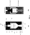
- FIG. 1 shows a monolithic integrated electro-optical device 10 according to an embodiment of the invention, in particular a cross-section of the electro-optical device 10.
- the device 10 is particularly a III-V-on-Si ridge electro optical device.
- the electro-optical device 10 of FIG. 1 may in particular be a Laser, a LED, or an optical amplifier.
- the electro-optical device 10 may be fabricated using the nanoridge ART approach.
- the device 10 particularly comprises a first-conductivity-type Si-based support region 11.
- the support region 11 may be a Si or Si-based (e.g. SiN) substrate.
- the support region 11 may also be a first-conductivity-type top region of an intrinsic Si or Si-based substrate, particularly of a SOI substrate.
- the device 10 further comprises a III-V-semiconductor-material ridge structure 12 extending from the Si-based support region 11, wherein the ridge structure 12 contains a recombination region 13.
- the ridge structure 12 may be fabricated using the ART approach on the support region 11, i.e. may be grown in a high-aspect-ratio trench formed before in the support region.
- the ridge structure 12 may extend on the support region 11 along a direction, which is into the plane in the cross-section shown in FIG. 1 .
- the device 10 further comprises a III-V-semiconductor capping layer 14 having a higher band-gap than the III-V semiconductor material of the ridge structure 12 and being provided on an outer surface of the ridge structure 12.
- the capping layer 14 is shown to encapsulate the ridge structure 12.
- the capping layer 14 may also surround only part of the ridge structure 12, i.e. may only be provided on parts of the outer surface of the ridge structure 12.
- the ridge structure 12 comprises a narrower portion arranged on the support region 11, and a wider portion carried on the narrower portion. In this case, the capping layer 14 may at least be provided on the outer surface of the wider portion.
- the device 10 finally comprises at least one second-conductivity-type III-V-semiconductor fin structure 15, which is narrower than and extends upwards from the top surface of the ridge structure 12. In particular, it extends upwards through an opening 16 formed in the capping layer 15, which is provided on the top surface of the ridge structure 12. After the forming of this opening, capping layer material remains on the top surface on both sides of the opening.
- the fin structure 15 may be at least 50% narrower than the width of the top surface of the ridge structure, i.e. it may be half as wide as the ridge structure at its top surface.
- the fin structure 15 may even be 60%, 70% or even 80% narrower than the top surface of the ridge structure 12.
- the ridge structure 12 i.e.
- the width of the fin structure 15 may vary.
- the fin structure 15 width may vary periodically from wider to narrower and again wider.
- the extension direction of the ridge structure 12 there may even be arranged a plurality of fin structures 15 one after the other.
- This arrangement can also be considered as a fin structure 15 with varying width along the extension direction of the ridge structure 12, wherein the width becomes zero in selected parts.
- the fin structure 15 is not formed by etching as in the device shown in FIG. 5 , but is provided on top of the ridge structure 12 after the ridge structure 12 and the capping layer 14 are made.
- the fin structure 12 may be regrown, i.e. grown on the ridge structure 12 after the ridge structure 12 is grown, and after an opening in the capping layer 14 on the ridge structure 12 is formed.
- the first-conductivity-type may be n-type and the second-conductivity-type p-type.
- First-conductivity-type charge carriers are thus electrons, and second-conductivity-type charge carriers are holed.
- these polarities could also be exchanged.
- FIG. 2 shows in (a) an electro-optical device 10 according to an embodiment of the invention, in particular a cross-section of the electro-optical device, which builds on the device 10 shown in FIG. 1 . Further, FIG. 2 shows in (b) an exemplary doping density in the device 10 shown in (a).
- FIG. 2 (b) exemplarily assumes that the first-conductivity-type is n-type, and the second-conductivity-type is p-type. Same elements in FIG. 1 and FIG. 2 share the same reference signs and function likewise. Accordingly, also the device 10 shown in FIG. 2 (a) includes the Si-based support region 11, the III-V semiconductor material ridge structure 12, the III-V semiconductor capping layer 14, and the fin structure 15.
- FIG. 2 further shows that the ridge structure 12 may include a narrower portion 23 arranged on the support region 11, e.g. in a STI trench and/or V-groove 26 formed in the support region 11, and a wider portion 22 arranged on top of the narrower portion 23. That is the wider portion 22 is freestanding supported by the narrower portion 23.
- the ridge structure 12 in other words is a freestanding ridge structure with a narrower foot and a wider body.
- FIG. 2 shows that the ridge structure 12, the capping layer 14 and the fin structure 15 may be surrounded by a dielectric 24, e.g. an oxide like SiO 2 .
- the fin structure 15 may be grown in a trench, which is provided in (e.g. etched into) the surrounding dielectric 24, wherein the dielectric trench is arranged above the ridge structure 12.
- the electro-optical device 10 may include a first electrode 21, which is in electrical contact with the fin structure 15.
- the first electrode 21 is particularly configured to inject second-conductivity-type charge carriers into the ridge structure 12, and also to collect excess first-conductivity-type charge carriers from the ridge structure 12, i.e. such first-conductivity-type charge carriers that did not recombine in the recombination region 13.
- the device 10 may also include a second electrode 25, which is in electrical contact with the support region 11.
- the second electrode 25 is configured to inject first-conductivity-type charge carriers into the ridge structure 12, and also to collect excess second-conductivity-type charge carriers from the ridge structure 12, i.e.
- the first and/or the second electrode may be a metal contact or plug, e.g. formed by using W, Cu or another suitable metal.
- the fin structure 15 which is in particular not obtained by etching it from/out of the ridge structure 12, but the fin structure 15 is grown on top of the ridge structure 12, i.e. it is regrown after growing and further preparing the ridge structure 12. Thereby, a ridge structure/fin structure interface 20 is formed.
- a fabrication of the device 10, and in particular of the fin structure 15, may thus include the following steps:
- FIG. 3 shows schematically a method 30 for fabricating the device 10 according to an embodiment of the invention.
- the method 30 includes at least the following steps.
- a plurality of electro-optical devices 10 may be fabricated in parallel, particularly by providing a plurality of ridge structures 12 at the same time next to another on the Si-based support region.
- the Si-based support region 11 may belong to (or be) a full wafer, particularly a 200 mm or 300 mm wafer.
- the wafer may finally be diced, in order to separate individual electro-optical devices 10.
- a plurality of STI trenches may be formed in the support region 11, and a ridge structure 12 may be epitaxially grown in each of the STI trenches.
- the method 30 is, due to its relative simplicity, able to achieve high yields of fabricating the electro-optical devices 10.
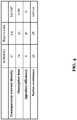
- FIG. 4 shows an overview of some parameters of the electro-optical device 10 including the regrown fin structure 15 comparison to the example device with the etched fin structure. It can be seen from the table shown in FIG. 4 that the device 10 according to embodiments of the present invention shows better (lower) transparency current density, lower absorption loss, higher injection efficiency, and only a marginally higher series resistance.
- the embodiments of the invention base on forming the fin structure 15 on the ridge structure 12, instead of etching it from the ridge structure 12.
- the laser mode of the electro-optical device 10 will have lower absorption loss, because on the one hand the mode is pushed away from the electrode 21, but still has acceptable injection efficiency, because non-radiative recombination at the surface or defects is prevented.
Landscapes
- Physics & Mathematics (AREA)
- Condensed Matter Physics & Semiconductors (AREA)
- General Physics & Mathematics (AREA)
- Electromagnetism (AREA)
- Optics & Photonics (AREA)
- Geometry (AREA)
- Semiconductor Lasers (AREA)
Priority Applications (2)
| Application Number | Priority Date | Filing Date | Title |
|---|---|---|---|
| EP18215210.8A EP3671982A1 (de) | 2018-12-21 | 2018-12-21 | Opto-elektronische iii-v-on-silicium-nanoridge-vorrichtung mit einer nachgewachsenen rippenstruktur |
| US16/719,894 US20200203930A1 (en) | 2018-12-21 | 2019-12-18 | Iii-v-on-silicon nanoridge opto-electronic device with a regrown fin structure |
Applications Claiming Priority (1)
| Application Number | Priority Date | Filing Date | Title |
|---|---|---|---|
| EP18215210.8A EP3671982A1 (de) | 2018-12-21 | 2018-12-21 | Opto-elektronische iii-v-on-silicium-nanoridge-vorrichtung mit einer nachgewachsenen rippenstruktur |
Publications (1)
| Publication Number | Publication Date |
|---|---|
| EP3671982A1 true EP3671982A1 (de) | 2020-06-24 |
Family
ID=64755460
Family Applications (1)
| Application Number | Title | Priority Date | Filing Date |
|---|---|---|---|
| EP18215210.8A Withdrawn EP3671982A1 (de) | 2018-12-21 | 2018-12-21 | Opto-elektronische iii-v-on-silicium-nanoridge-vorrichtung mit einer nachgewachsenen rippenstruktur |
Country Status (2)
| Country | Link |
|---|---|
| US (1) | US20200203930A1 (de) |
| EP (1) | EP3671982A1 (de) |
Cited By (2)
| Publication number | Priority date | Publication date | Assignee | Title |
|---|---|---|---|---|
| WO2022189285A1 (en) * | 2021-03-12 | 2022-09-15 | Sony Semiconductor Solutions Corporation | Time-of-flight portion and time-of-flight portion manufacturing method |
| EP4576453A1 (de) * | 2023-12-22 | 2025-06-25 | Imec VZW | Elektrooptische vorrichtung auf basis von iii-v- und/oder ii-vi- und/oder gruppe iv-halbleitern und verfahren |
Citations (3)
| Publication number | Priority date | Publication date | Assignee | Title |
|---|---|---|---|---|
| US5978402A (en) * | 1996-12-11 | 1999-11-02 | Mitsubishi Denki Kabushiki Kaisha | Semiconductor laser device |
| US6359919B1 (en) * | 1996-07-26 | 2002-03-19 | Kabushiki Kaisha Toshiba | Gallium nitride-based compound semiconductor laser and method of manufacturing the same |
| US20030020079A1 (en) * | 2001-07-27 | 2003-01-30 | Sanyo Electric Co., Ltd. | Nitride-based semiconductor light-emitting device and method of fabricating the same |
-
2018
- 2018-12-21 EP EP18215210.8A patent/EP3671982A1/de not_active Withdrawn
-
2019
- 2019-12-18 US US16/719,894 patent/US20200203930A1/en not_active Abandoned
Patent Citations (3)
| Publication number | Priority date | Publication date | Assignee | Title |
|---|---|---|---|---|
| US6359919B1 (en) * | 1996-07-26 | 2002-03-19 | Kabushiki Kaisha Toshiba | Gallium nitride-based compound semiconductor laser and method of manufacturing the same |
| US5978402A (en) * | 1996-12-11 | 1999-11-02 | Mitsubishi Denki Kabushiki Kaisha | Semiconductor laser device |
| US20030020079A1 (en) * | 2001-07-27 | 2003-01-30 | Sanyo Electric Co., Ltd. | Nitride-based semiconductor light-emitting device and method of fabricating the same |
Cited By (2)
| Publication number | Priority date | Publication date | Assignee | Title |
|---|---|---|---|---|
| WO2022189285A1 (en) * | 2021-03-12 | 2022-09-15 | Sony Semiconductor Solutions Corporation | Time-of-flight portion and time-of-flight portion manufacturing method |
| EP4576453A1 (de) * | 2023-12-22 | 2025-06-25 | Imec VZW | Elektrooptische vorrichtung auf basis von iii-v- und/oder ii-vi- und/oder gruppe iv-halbleitern und verfahren |
Also Published As
| Publication number | Publication date |
|---|---|
| US20200203930A1 (en) | 2020-06-25 |
Similar Documents
| Publication | Publication Date | Title |
|---|---|---|
| CN113396486B (zh) | 具有电介质dbr的磷化铟vcsel | |
| US7348607B2 (en) | Planar avalanche photodiode | |
| JP4056481B2 (ja) | 半導体素子およびその製造方法 | |
| JPS61502434A (ja) | 埋込みへテロ構造を有する半導体デバイス | |
| KR101300298B1 (ko) | Vcsel 및 vcsel의 제조 방법 | |
| US20190101711A1 (en) | Active-Passive Waveguide Photonic System | |
| US10690852B2 (en) | III-V semiconductor waveguide nanoridge structure | |
| US10554018B2 (en) | Hybrid vertical current injection electro-optical device with refractive-index-matched current blocking layer | |
| US20200203930A1 (en) | Iii-v-on-silicon nanoridge opto-electronic device with a regrown fin structure | |
| EP0527615A1 (de) | Verfahren zur Herstellung eines abstimmbaren Halbleiterlasers | |
| US20180278025A1 (en) | Laterally grown edge emitting laser | |
| Wierer et al. | Buried tunnel contact junction AlGaAs-GaAs-InGaAs quantum well heterostructure lasers with oxide-defined lateral currents | |
| US7319076B2 (en) | Low resistance T-shaped ridge structure | |
| US7986721B2 (en) | Semiconductor optical device including a PN junction formed by a second region of a first conductive type semiconductor layer and a second conductive type single semiconductor layer | |
| JP2008288284A (ja) | 半導体光素子及びその製造方法 | |
| EP3671981A1 (de) | Opto-elektronische iii-v-on-silicium-nanoridge-vorrichtung mit trägerblockierungsschichten | |
| US4989050A (en) | Self aligned, substrate emitting LED | |
| WO2003077380A2 (en) | A laser diode with a low absorption diode junction | |
| KR20050085176A (ko) | 표면 발광 반도체 레이저의 매입된 터널 접합부 제조 방법 | |
| US20250208444A1 (en) | Electro-optical devices having ridge semiconductor structure and methods of fabricating the same | |
| JP2007251220A (ja) | 半導体素子およびその製造方法 | |
| US20030062517A1 (en) | Semiconductor device with current confinement structure | |
| JP4461980B2 (ja) | 半導体光素子 | |
| US6751246B2 (en) | Buried ribbon semiconductor laser and a method of fabrication | |
| US20030119222A1 (en) | Hybrid confinement layers of buried heterostructure semiconductor laser |
Legal Events
| Date | Code | Title | Description |
|---|---|---|---|
| PUAI | Public reference made under article 153(3) epc to a published international application that has entered the european phase |
Free format text: ORIGINAL CODE: 0009012 |
|
| STAA | Information on the status of an ep patent application or granted ep patent |
Free format text: STATUS: THE APPLICATION HAS BEEN PUBLISHED |
|
| AK | Designated contracting states |
Kind code of ref document: A1 Designated state(s): AL AT BE BG CH CY CZ DE DK EE ES FI FR GB GR HR HU IE IS IT LI LT LU LV MC MK MT NL NO PL PT RO RS SE SI SK SM TR |
|
| AX | Request for extension of the european patent |
Extension state: BA ME |
|
| STAA | Information on the status of an ep patent application or granted ep patent |
Free format text: STATUS: THE APPLICATION IS DEEMED TO BE WITHDRAWN |
|
| 18D | Application deemed to be withdrawn |
Effective date: 20210112 |