EP3667893A1 - Power conversion device - Google Patents
Power conversion device Download PDFInfo
- Publication number
- EP3667893A1 EP3667893A1 EP17920796.4A EP17920796A EP3667893A1 EP 3667893 A1 EP3667893 A1 EP 3667893A1 EP 17920796 A EP17920796 A EP 17920796A EP 3667893 A1 EP3667893 A1 EP 3667893A1
- Authority
- EP
- European Patent Office
- Prior art keywords
- submodule
- terminal
- circuit
- submodules
- type converter
- Prior art date
- Legal status (The legal status is an assumption and is not a legal conclusion. Google has not performed a legal analysis and makes no representation as to the accuracy of the status listed.)
- Granted
Links
Images




Classifications
-
- H—ELECTRICITY
- H02—GENERATION; CONVERSION OR DISTRIBUTION OF ELECTRIC POWER
- H02M—APPARATUS FOR CONVERSION BETWEEN AC AND AC, BETWEEN AC AND DC, OR BETWEEN DC AND DC, AND FOR USE WITH MAINS OR SIMILAR POWER SUPPLY SYSTEMS; CONVERSION OF DC OR AC INPUT POWER INTO SURGE OUTPUT POWER; CONTROL OR REGULATION THEREOF
- H02M7/00—Conversion of AC power input into DC power output; Conversion of DC power input into AC power output
- H02M7/003—Constructional details, e.g. physical layout, assembly, wiring or busbar connections
-
- H—ELECTRICITY
- H02—GENERATION; CONVERSION OR DISTRIBUTION OF ELECTRIC POWER
- H02M—APPARATUS FOR CONVERSION BETWEEN AC AND AC, BETWEEN AC AND DC, OR BETWEEN DC AND DC, AND FOR USE WITH MAINS OR SIMILAR POWER SUPPLY SYSTEMS; CONVERSION OF DC OR AC INPUT POWER INTO SURGE OUTPUT POWER; CONTROL OR REGULATION THEREOF
- H02M7/00—Conversion of AC power input into DC power output; Conversion of DC power input into AC power output
- H02M7/42—Conversion of DC power input into AC power output without possibility of reversal
- H02M7/44—Conversion of DC power input into AC power output without possibility of reversal by static converters
- H02M7/48—Conversion of DC power input into AC power output without possibility of reversal by static converters using discharge tubes with control electrode or semiconductor devices with control electrode
- H02M7/483—Converters with outputs that each can have more than two voltages levels
-
- H—ELECTRICITY
- H02—GENERATION; CONVERSION OR DISTRIBUTION OF ELECTRIC POWER
- H02M—APPARATUS FOR CONVERSION BETWEEN AC AND AC, BETWEEN AC AND DC, OR BETWEEN DC AND DC, AND FOR USE WITH MAINS OR SIMILAR POWER SUPPLY SYSTEMS; CONVERSION OF DC OR AC INPUT POWER INTO SURGE OUTPUT POWER; CONTROL OR REGULATION THEREOF
- H02M7/00—Conversion of AC power input into DC power output; Conversion of DC power input into AC power output
- H02M7/42—Conversion of DC power input into AC power output without possibility of reversal
- H02M7/44—Conversion of DC power input into AC power output without possibility of reversal by static converters
- H02M7/48—Conversion of DC power input into AC power output without possibility of reversal by static converters using discharge tubes with control electrode or semiconductor devices with control electrode
- H02M7/483—Converters with outputs that each can have more than two voltages levels
- H02M7/4835—Converters with outputs that each can have more than two voltages levels comprising two or more cells, each including a switchable capacitor, the capacitors having a nominal charge voltage which corresponds to a given fraction of the input voltage, and the capacitors being selectively connected in series to determine the instantaneous output voltage
-
- H—ELECTRICITY
- H02—GENERATION; CONVERSION OR DISTRIBUTION OF ELECTRIC POWER
- H02M—APPARATUS FOR CONVERSION BETWEEN AC AND AC, BETWEEN AC AND DC, OR BETWEEN DC AND DC, AND FOR USE WITH MAINS OR SIMILAR POWER SUPPLY SYSTEMS; CONVERSION OF DC OR AC INPUT POWER INTO SURGE OUTPUT POWER; CONTROL OR REGULATION THEREOF
- H02M7/00—Conversion of AC power input into DC power output; Conversion of DC power input into AC power output
- H02M7/42—Conversion of DC power input into AC power output without possibility of reversal
- H02M7/44—Conversion of DC power input into AC power output without possibility of reversal by static converters
- H02M7/48—Conversion of DC power input into AC power output without possibility of reversal by static converters using discharge tubes with control electrode or semiconductor devices with control electrode
- H02M7/53—Conversion of DC power input into AC power output without possibility of reversal by static converters using discharge tubes with control electrode or semiconductor devices with control electrode using devices of a triode or transistor type requiring continuous application of a control signal
- H02M7/537—Conversion of DC power input into AC power output without possibility of reversal by static converters using discharge tubes with control electrode or semiconductor devices with control electrode using devices of a triode or transistor type requiring continuous application of a control signal using semiconductor devices only, e.g. single switched pulse inverters
- H02M7/5387—Conversion of DC power input into AC power output without possibility of reversal by static converters using discharge tubes with control electrode or semiconductor devices with control electrode using devices of a triode or transistor type requiring continuous application of a control signal using semiconductor devices only, e.g. single switched pulse inverters in a bridge configuration
Definitions
- the present disclosure relates to a self-exciting power conversion device formed by cascade-connecting a plurality of converter cells and suitably used in, for example, high-voltage direct-current power transmission, a frequency converter and the like.
- a modular multilevel converter is known as a large-capacity power conversion device connected to a power system.
- the modular multilevel converter has, for each phase of an alternating current, an upper arm circuit connected to a high potential-side DC node and a lower arm circuit connected to a low potential-side DC node.
- Each arm circuit is formed by cascade-connecting multiple converter cells.
- Each converter cell includes a capacitor serving as an energy accumulator, first and second input/output nodes, and a bridge circuit configured to perform switching between connection and non-connection of a portion between these input/output nodes and the capacitor.
- a half bridge-type circuit, a full bridge-type circuit or the like is used as the bridge circuit.
- a method commonly used in an actual high-voltage converter is a method for forming a block from a plurality of converter cells, and vertically stacking the blocks to form a tower (see, for example, Fig. 5 in PTL 1 (International Publication No. 2016/162915 )).
- each block is arranged in a tray of an insulator.
- Half bridge-type converter cells and full bridge-type converter cells may be arranged in a mixed manner to form each arm circuit in some cases.
- a half of a plurality of converter cells forming each arm circuit are full bridge-type converter cells and the other half are half bridge-type converter cells.
- a tower formed only of the full bridge-type converter cells and a tower formed only of the half bridge-type converter cells can be provided.
- each arm circuit includes only a few (e.g., two to three) full bridge-type converter cells
- half bridge-type converter cells and the full bridge-type converter cells must be arranged in a mixed manner in one tower. This causes a problem in terms of space efficiency because the half bridge-type converter cells and the full bridge-type converter cells differ in size.
- the present disclosure has been made in view of the above-described problem and an object of the present disclosure is to provide an MMC-type power conversion device in which half bridge-type converter cells and full bridge-type converter cells can be arranged with high space efficiency.
- the power conversion device according to the present disclosure is widely applicable to the case in which half bridge-type converter cells and full bridge-type converter cells are arranged in a mixed manner, regardless of the number of the converter cells.
- a power conversion device includes a plurality of submodules connected in series to each other.
- Each of the plurality of submodules includes: a first terminal, a second terminal and a third terminal; a first semiconductor switching element; a second semiconductor switching element; and a DC capacitor.
- the first terminal, the second terminal and the third terminal are provided on or provided to protrude from a surface of a package.
- the first semiconductor switching element is built into the package and connected between the first terminal and the second terminal.
- the second semiconductor switching element is built into the package and connected between the second terminal and the third terminal.
- the DC capacitor is built into the package and connected between the first terminal and the third terminal.
- the plurality of submodules include a first submodule and a second submodule that are adjacent to each other.
- the first terminal of the first submodule and the first terminal of the second submodule are connected to each other through a wiring.
- the third terminal of the first submodule and the third terminal of the second submodule are connected to
- a single submodule can be used as a half bridge-type converter cell, and two adjacent submodules can be used as a full bridge-type converter cell by connecting terminals thereof to each other. Therefore, half bridge-type converter cells and full bridge-type converter cells can be arranged with high space efficiency.
- Fig. 1 is a schematic configuration diagram showing an example power conversion device.
- the power conversion device includes leg circuits 4u, 4v and 4w (which are denoted as a leg circuit 4 when they are collectively referred to or an unspecified one is referred to) serving as main circuits, and a central controller 3 configured to control leg circuit 4.
- Leg circuit 4 is provided for each of a plurality of phases forming an alternating current. Leg circuit 4 is connected between an AC circuit 20 and a DC circuit 21, and performs power conversion between these circuits.
- Fig. 1 shows the case in which AC circuit 20 is a three-phase AC circuit, and three leg circuits 4u, 4v and 4w are provided to correspond to a U phase, a V phase and a W phase, respectively.
- AC nodes Nu, Nv and Nw provided in leg circuits 4u, 4v and 4w, respectively, are connected to AC circuit 20 with an interconnection transformer 22 being interposed.
- AC circuit 20 is, for example, an AC power system including an AC power supply and the like.
- Fig. 1 does not show connection of AC nodes Nv and Nw to interconnection transformer 22.
- DC nodes Np and Nn i.e., high potential-side DC node Np and low potential-side DC node Nn
- DC circuit 21 corresponds to a connection wiring to a DC power system in a high-voltage direct-current (HVDC) system or another power conversion device in a BTB (Back To Back) system.
- HVDC high-voltage direct-current
- the HVDC system is configured to convert high-voltage AC power to DC power and perform DC long-distance power transmission.
- Power conversion device 1 in Fig. 1 is used for this AC/DC conversion.
- the BTB system is configured to perform forward conversion for converting AC to DC and reverse conversion for converting DC to AC, thereby implementing power interchange between two AC circuits.
- Power conversion device 1 in Fig. 1 is used for the forward conversion and the reverse conversion.
- AC nodes Nu, Nv and Nw may be connected to AC circuit 20 with an interconnection reactor being interposed.
- AC circuit 20 and each leg circuit 4 may be connected in an AC manner. A detailed configuration of a connection portion connecting AC circuit 20 and each leg circuit 4 in this case will be described below.
- Leg circuit 4u is separated into a high potential-side arm circuit (also referred to as “upper arm circuit” or “primary arm circuit”) 10 extending from high potential-side DC node Np to AC node Nu, and a low potential-side arm circuit (also referred to as “lower arm circuit” or “secondary arm circuit”) 11 extending from low potential-side DC node Nn to AC node Nu.
- a connection point Nu connecting high potential-side arm circuit 10 and low potential-side arm circuit 11 is connected to transformer 22.
- High potential-side DC node Np and low potential-side DC node Nn are connected to DC circuit 21.
- Leg circuits 4v and 4w have a similar configuration, and thus, leg circuit 4u will be described below as a typical example.
- High potential-side arm circuit 10 includes a plurality of half bridge (HB)-type converter cells 5, one or more full bridge (FB)-type converter cells 6, and a reactor 7a.
- the plurality of converter cells 5, at least one converter cell 6 and reactor 7a are connected in series to each other.
- the converter cell may be simply referred to as "cell”.
- Half bridge-type converter cells 5 and one or more full bridge-type converter cells 6 may be connected in any order.
- low potential-side arm circuit 11 includes a plurality of half bridge-type converter cells 5, one or more full bridge-type converter cells 6, and a reactor 7b.
- the plurality of converter cells 5, at least one converter cell 6 and reactor 7b are connected in series to each other.
- Half bridge-type converter cells 5 and one or more full bridge-type converter cells 6 may be connected in any order.
- Reactors 7a and 7b are provided such that arm currents Ipu and Ipn do not rapidly change at the moment when the cells in each leg circuit are turned on or off and an output voltage rapidly changes or when AC circuit 20, DC circuit 21 or the like fails.
- a position where reactor 7a is inserted may be any position in high potential-side arm circuit 10 of leg circuit 4u, and a position where reactor 7b is inserted may be any position in low potential-side arm circuit 11 of leg circuit 4u.
- a plurality of reactors 7a may be provided and a plurality of reactors 7b may be provided. The reactors may be different from each other in inductance value. Furthermore, only reactor 7a of high potential-side arm circuit 10 or only reactor 7b of low potential-side arm circuit 11 may be provided.
- power conversion device 1 in Fig. 1 further includes an AC voltage detector 23, an AC current detector 24, DC voltage detectors 25p and 25n, and arm current detectors 9a and 9b provided in each leg circuit 4. Signals detected by these detectors are input to central controller 3.
- AC voltage detector 23 detects a voltage value Vacu of the U phase of AC circuit 20, a voltage value Vacv of the V phase of AC circuit 20, and a voltage value Vacw of the W phase of AC circuit 20.
- AC current detector 24 detects a current value Iacu of the U phase of AC circuit 20, a current value Iacv of the V phase of AC circuit 20, and a current value Iacw of the W phase of AC circuit 20.
- DC voltage detector 25p detects a voltage of high potential-side DC node Np connected to DC circuit 21.
- DC voltage detector 25n detects a voltage of low potential-side DC node Nn connected to DC circuit 21.
- arm current detectors 9a and 9b provided in leg circuit 4u for the U phase detect arm current Ipu flowing through high potential-side arm circuit 10 and arm current Inu flowing through low potential-side arm circuit 11, respectively.
- arm current detectors 9a and 9b provided in leg circuit 4v for the V phase detect a high potential-side arm current Ipv and a low potential-side arm current Inv, respectively.
- Arm current detectors 9a and 9b provided in leg circuit 4w for the W phase detect a high potential-side arm current Ipw and a low potential-side arm current Inw, respectively. Based on these arm currents, a DC current Idc flowing through DC circuit 21 and a circulating current circulating among the leg circuits can be calculated.
- the signals detected by the above-described detectors are input to central controller 3.
- Central controller 3 further receives, from each cell 5, 6, a signal indicating a detection value of a cell capacitor voltage. Based on the signals detected by the above-described detectors and the information about the cell capacitor voltages, central controller 3 outputs, to each cell 5, 6, a control instruction for controlling an operation state of each cell 5, 6 and an operation/stop instruction (an operation instruction or a stop instruction) for protecting each cell 5, 6.
- Fig. 1 collectively shows a part of signal lines for the signals input from the detectors to central controller 3 and a part of signal lines for the signals transmitted between central controller 3 and cells 5.
- the signal line is individually provided for each detector and for each cell 5, 6.
- a signal line for transmission and a signal line for reception may be separately provided between each cell 5, 6 and central controller 3.
- these signal lines are formed of optical fibers from the viewpoint of noise resistance.
- Central controller 3 is formed by a circuit and can be formed by, for example, at least one microcomputer, or at least one ASIC (Application Specific Integrated Circuit), or at least one FPGA (Field Programmable Gate Array). Alternatively, central controller 3 may be formed by combining any of the foregoing.
- the microcomputer includes at least one processor (e.g., a CPU (Central Processing Unit)).
- the processor can execute all or a part of functions of central controller 3 by reading one or more commands from at least one computer-readable non-transitory storage medium (such as, for example, a magnetic medium such as a hard disk, an optical medium such as a CD (Compact Disk) and a DVD (Digital Video Disk), and a semiconductor memory).
- Fig. 1 shows an example in which AC circuit 20 and a power conversion circuit portion 2 are connected in a DC manner through AC nodes Nu, Nv and Nw provided in leg circuits 4u, 4v and 4w, respectively.
- AC circuit 20 and each leg circuit 4 may be connected in an AC manner with a transformer being interposed.
- Fig. 2 shows a modification of a connection portion connecting the AC circuit and each leg circuit.
- AC circuit 20 and each of leg circuits 4u, 4v and 4w are connected with a three-phase transformer 80B being interposed.
- primary windings 81u, 81v and 81w are ⁇ -connected. Specifically, primary winding 81u of three-phase transformer 80B is connected between the U phase and the V phase of AC circuit 20. Primary winding 81v of three-phase transformer 80B is connected between the V phase and the W phase of AC circuit 20. Primary winding 81w of three-phase transformer 80B is connected between the W phase and the U phase of AC circuit 20.
- Secondary windings 82u, 82v and 82w of three-phase transformer 80B are magnetically coupled to primary windings 81u, 81v and 81w, respectively, with a common iron core being interposed. Furthermore, secondary winding 82u is connected in series to arm circuits 10u and 11u of the U phase, secondary winding 82v is connected in series to arm circuits 10v and 11v of the V phase, and secondary winding 82w is connected in series to arm circuits 10w and 11w of the W phase.
- each of secondary windings 82u, 82v and 82w functions as reactors 7a and 7b of each phase.
- secondary windings 82u, 82v and 82w of three-phase transformer 80B may be provided separately from reactors 7a and 7b.
- a DC magnetic flux generated in the iron core can be canceled out by flowing a DC component through ⁇ -connected primary windings 81u, 81v and 81w.
- Fig. 3 shows another modification of the connection portion connecting the AC circuit and each leg circuit.
- AC circuit 20 and each of leg circuits 4u, 4v and 4w are connected with a three-phase transformer 80C of three windings being interposed.
- one ends of primary windings 81u, 81v and 81w of three-phase transformer 80C in Fig. 3 are connected to power transmission lines of the U phase, the V phase and the W phase of AC circuit 20, respectively, with interconnection transformer 22 being interposed.
- the other ends of primary windings 81u, 81v and 81w of three-phase transformer 80C are connected to a common neutral point 84. That is, in the case of Fig. 3 , primary windings 81u, 81v and 81w are Y-connected.
- Secondary windings 82u, 82v and 82w of three-phase transformer 80C are magnetically coupled to primary windings 81u, 81v and 81w, respectively, with a common iron core being interposed.
- tertiary windings 83u, 83v and 83w connected in series to secondary windings 82u, 82v and 82w, respectively, are further provided.
- the secondary winding of each phase and the corresponding tertiary winding are connected so as to be opposite in polarity, and are wound around the common iron core.
- a connection point connecting the secondary winding of each phase and the corresponding tertiary winding is connected to a common neutral point 810.
- secondary winding 82u and tertiary winding 83u are connected in series to arm circuits 10u and 11u of the U phase.
- Secondary winding 82v and tertiary winding 83v are connected in series to arm circuits 10v and 11v of the V phase.
- Secondary winding 82w and tertiary winding 83w are connected in series to arm circuits 10w and 11w of the W phase.
- each of secondary windings 82u, 82v and 82w and each of tertiary windings 83u, 83v and 83w also function as reactors 7a and 7b of each phase.
- Secondary windings 82u, 82v and 82w and tertiary windings 83u, 83v and 83w of three-phase transformer 80C may be provided separately from reactors 7a and 7b.
- Three-phase transformer 80C in Fig. 3 has an advantage that the DC electromotive force generated in the secondary windings and the electromotive force generated in the tertiary windings are canceled out because of the arm currents (U phase: Ipu, Inu; V phase: Ipv, Inv; W phase: Ipw, Inw) of the respective phases, and thus, a DC magnetic flux is not generated in the iron core.
- half bridge-type converter cell 5 is formed as a single packaged submodule 40.
- Full bridge-type converter cell 6 is formed by combining two submodules 40. This brings about an advantage that arm circuits 10 and 11 in which the half bridge-type converter cells and the full bridge-type converter cells are arranged in a mixed manner can be formed only by submodules 40 having the same shape and size. Description will be given below with reference to the drawings.
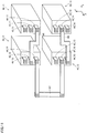
- Fig. 4 shows an example circuit configuration of the submodule.
- Fig. 4(A) shows an example in which one full bridge-type converter cell is formed by combining two submodules 40_1 and 40_2.
- underbars and identification numbers are assigned after the reference characters.
- each submodule 40 includes a package 41, an AC terminal 42, a positive-side terminal 43, a negative-side terminal 44, semiconductor switching elements 45 and 46, diodes 47 and 48, and a DC capacitor 49 serving as an energy accumulator.
- Package 41 includes, for example, a case made of resin.
- AC terminal 42, positive-side terminal 43 and negative-side terminal 44 are provided on or provided to protrude from a surface of package 41.
- Semiconductor switching element 45 is connected between positive-side terminal 43 and AC terminal 42.
- Semiconductor switching element 46 is connected between AC terminal 42 and negative-side terminal 44.
- a self-exciting semiconductor switching element such as an IGBT (Insulated Gate Bipolar Transistor) or a GCT (Gate Commutated Turn-off thyristor) is, for example, used as semiconductor switching elements 45 and 46.
- Diodes 47 and 48 are connected in antiparallel (i.e., in parallel and in a reverse bias direction) to semiconductor switching elements 45 and 46, respectively. Diodes 47 and 48 are provided to ensure a current path when a reverse voltage is applied to corresponding semiconductor switching elements 45 and 46.
- DC capacitor 49 is connected between positive-side terminal 43 and negative-side terminal 44. Therefore, DC capacitor 49 is connected in parallel to semiconductor switching elements 45 and 46 connected in series to each other.
- a positive-side terminal 43_1 of one submodule 40_1 and a positive-side terminal 43_2 of the other submodule 40_2 are connected through a wiring 60.
- a negative-side terminal 44_1 of one submodule 40_1 and a negative-side terminal 44_2 of the other submodule 40_2 are connected through a wiring 61.
- An AC terminal 42_1 of submodule 40_1 and an AC terminal 42_2 of submodule 40_2 are used for connection to other elements or the like that are adjacent on the low potential side.
- bus bar a conductor bar referred to as "bus bar” or a conductor plate
- a conductor bar a conductor bar referred to as "bus bar” or a conductor plate
- a bare wire, a metal pipe or the like may, for example, be used.
- Fig. 4(B) is an equivalent circuit diagram corresponding to Fig. 4(A) .
- positive-side terminals 43_1 and 43_2 coupled to each other as shown in Fig. 4(A) are replaced with one positive-side node 43A.
- Negative-side terminals 44_1 and 44_2 coupled to each other as shown in Fig. 4(A) are replaced with one negative-side node 44A.
- DC capacitors 49_1 and 49_2 connected in parallel as shown in Fig. 4(A) are replaced with one DC capacitor 50.
- full bridge-type converter cell 6 can be formed by the connection between the terminals shown in Fig. 4(A) .
- Fig. 5 is a perspective view schematically showing a physical appearance of the submodule.
- a front/back direction is referred to as "X direction”
- a right/left direction is referred to as “Y direction”
- an up/down direction is referred to as "Z direction”.
- Fig. 5(A) shows an example appearance of single submodule 40.
- submodule 40 has package 41 having a substantially rectangular parallelepiped shape with the X direction being a longitudinal direction.
- AC terminal 42, positive-side terminal 43 and negative-side terminal 44 are provided on a front surface (surface on the +X direction side) of package 41.
- positive-side terminal 43, AC terminal 42 and negative-side terminal 44 are aligned in this order from above.
- this order of alignment is merely one example and the present disclosure is not limited thereto.
- Fig. 5(B) shows an appearance diagram when one full bridge-type converter cell is formed by combining two submodules 40_1 and 40_2.
- submodules 40_1 and 40_2 are arranged side by side in the right/left direction. As a result, the terminals provided in each submodule 40 are arranged to face the common front surface side. As shown in the figure, positive-side terminal 43_1 of one submodule 40_1 and positive-side terminal 43_2 of the other submodule 40_2 are connected through wiring 60. Furthermore, negative-side terminal 44_1 of one submodule 40_1 and negative-side terminal 44_2 of the other submodule 40_2 are connected through wiring 61. In the case of Fig. 5(B) , a conductor bar referred to as "bus bar" is used as wirings 60 and 61.
- Fig. 5 The above-described configuration in Fig. 5 is merely one example, and the shape of package 41 of submodule 40 and arrangement of AC terminal 42, positive-side terminal 43 and negative-side terminal 44 on the surface of package 41 are not limited to the example in Fig. 5 .
- positive-side terminal 43 is used only for connection between two submodules 40 forming the full bridge-type converter cell. Therefore, in Fig. 5(A) , AC terminal 42 and negative-side terminal 44 may be arranged on the front surface (surface on the +X side) of package 41 and positive-side terminal 43 may be arranged on a back surface (surface on the -X side) of package 41.
- Fig. 6 is a circuit diagram showing an example configuration of the high potential-side arm circuit.
- a circuit diagram in Fig. 6(A) shows an example in which full bridge-type converter cells are arranged in the proximity of a high potential-side DC line 26p connected to DC circuit 21.
- a circuit diagram in Fig. 6(B) shows an example in which a full bridge-type converter cell is arranged in the proximity of an AC line 27 connected to AC circuit 20.
- a circuit diagram in Fig. 6(C) shows an example in which half bridge-type converter cells and full bridge-type converter cells are arranged in a mixed manner.
- a plurality of submodules 40 are arranged in the order of submodules 40_1, 40_2, 40_3 ... from the high potential side.
- a full bridge-type converter cell is formed by submodules 40_1 and 40_2. Furthermore, a full bridge-type converter cell is formed by submodules 40_3 and 40_4. Submodule 40_5 is used as a half bridge-type converter cell.
- AC terminal 42_1 of submodule 40_1 is connected to DC line 26p.
- AC terminal 42_2 of submodule 40_2 and an AC terminal 42_3 of submodule 40_3 are connected through a wiring.
- An AC terminal 42_4 of submodule 40_4 and AC terminal 42_5 of submodule 40_5 are connected through a wiring.
- submodules 40_1 to 40_3 are used as half bridge-type converter cells.
- AC terminal 42_1 of submodule 40_1 is connected to DC line 26p.
- Negative-side terminal 44_1 of submodule 40_1 and AC terminal 42_2 of submodule 40_2 are connected through a wiring.
- Negative-side terminal 44_2 of submodule 40_2 and an AC terminal 42_3 of submodule 40_3 are connected through a wiring.
- AC terminals 42 and negative-side terminals 44 are used for connection to the adjacent elements.
- Positive-side terminals 43 are not used for connection.
- submodule 40_1 is used as a half bridge-type converter cell.
- a full bridge-type converter cell is formed by submodules 40_2 and 40_3.
- Submodule 40_4 is used as a half bridge-type converter cell.
- AC terminal 42_1 of submodule 40_1 is connected to DC line 26p.
- Negative-side terminal 44_1 of submodule 40_1 and AC terminal 42_2 of submodule 40_2 are connected through a wiring.
- AC terminal 42_3 of submodule 40_3 and AC terminal 42_4 of submodule 40_4 are connected through a wiring.
- each of AC terminal 42 of one submodule 40 and AC terminal 42 of the other submodule 40 is used for connection to the adjacent external element.
- positive-side terminals 43 are connected to each other and negative-side terminals 44 are connected to each other.
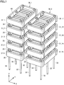
- Fig. 7 is a perspective view schematically showing a physical appearance of the arm circuit.
- a plurality of submodules 40 are aligned in the horizontal direction (Y direction) to form a block, and each block is arranged in a tray-like insulating container 31.
- a plurality of containers 31 are stacked vertically to form a tower 30.
- each insulating container 31 is formed by a bottom plate 35 having a substantially rectangular shape, and a side plate 34 standing from an edge portion of bottom plate 35.
- Lowermost insulating container 31 is supported by a plurality of support rods 32 standing on a floor surface.
- Each of insulating containers 31 provided above lowermost insulating container 31 is supported by a plurality of support rods 33 standing from lowermost insulating container 31.
- an arm circuit is formed by two towers 30_1 and 30_2.
- Tower 30_1 includes five insulating containers 31_1 to 31_5, and tower 30_2 includes five insulating containers 31_11 to 31_15.
- eight submodules 40 are arranged side by side in the horizontal direction (Y direction).
- Y direction the horizontal direction
- respective submodules 40 have the same shape, and thus, submodules 40 can be arranged with high space efficiency.
- connection between submodules 40 will be described in detail with reference to a specific example.
- Fig. 8 is a diagram for illustrating connection between the submodules forming the arm circuit.
- Fig. 8 shows an example in which high potential-side arm circuit 10 is formed by tower 30 including three-tier insulating containers 31_1 to 31_3.
- Six submodules 40 are arranged in each insulating container 31. Specifically, six submodules 40_1 to 40_6 are arranged in insulating container 31_1, six submodules 40_7 to 40_12 are arranged in insulating container 31_2, and six submodules 40_13 to 40_18 are arranged in insulating container 31_3. Submodule 40_1 is on the highest potential side and submodule 40_18 is on the lowest potential side.
- Submodules 40 are arranged horizontally, and thus, the terminals (i.e., positive-side terminal 43, AC terminal 42 and negative-side terminal 44) are provided on the front surface of each submodule 40. This facilitates connection between adjacent submodules 40.
- Fig. 9 is a diagram in which the arrangement of the submodules shown in Fig. 8 is replaced with arrangement of half bridge-type converter cells and full bridge-type converter cells.
- a full bridge-type converter cell is formed by submodules 40_1 and 40_2
- a full bridge-type converter cell is formed by submodules 40_3 and 40_4.
- the other submodules 40 are each used as a half bridge-type converter cell.
- submodule 40_1 and submodule 40_2 forming a full bridge-type converter cell positive-side terminals 43 are connected to each other and negative-side terminals 44 are connected to each other.
- AC terminal 42 of submodule 40_1 is connected to high potential-side DC line 26p of the DC circuit.
- AC terminal 42 of submodule 40_2 is connected to AC terminal 42 of submodule 40_3 that is adjacent on the low potential side.
- submodule 40_3 and submodule 40_4 forming a full bridge-type converter cell
- positive-side terminals 43 are connected to each other and negative-side terminals 44 are connected to each other.
- AC terminal 42 of submodule 40_3 is connected to AC terminal 42 of submodule 40_2 that is adjacent on the high potential side.
- AC terminal 42 of submodule 40_4 is connected to AC terminal 42 of submodule 40_5 that is adjacent on the low potential side.
- Each of submodules 40_5 to 40_18 forms a half bridge-type converter cell.
- AC terminal 42 of each submodule 40 is connected to negative-side terminal 44 of that submodule 40.
- AC terminal 42 of submodule 40 is connected to AC terminal 42 of that submodule 40.
- negative-side terminal 44 of each submodule 40 forming a half bridge-type converter cell is connected to AC terminal 42 of submodule 40 that is adjacent on the low potential side. Whether submodule 40 that is adjacent on the low potential side forms a half bridge-type converter cell or a full bridge-type converter cell, there is no difference. Negative-side terminal 44 of submodule 40_18 on the lowest potential side is connected to AC line 27 of AC circuit 20.
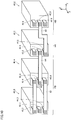
- Fig. 10 is an appearance diagram schematically showing mutual connection among submodules 40_3 to 40_6 in Fig. 8 .
- positive-side terminals 43_3 and 43_4 are connected to each other through a bus bar 62, and negative-side terminals 44_3 and 44_4 are connected to each other through a bus bar 63.
- Each of submodules 40_5 and 40_6 on the low potential side relative to submodule 40_4 is used as a half bridge-type converter cell.
- AC terminal 42_5 of submodule 40_5 is connected, through a bus bar 64, to AC terminal 42_4 of submodule 40_4 that is adjacent on the high potential side and forms a full bridge-type converter cell.
- Negative-side terminal 44_5 of submodule 40_5 is connected, through a bus bar 65, to AC terminal 42_6 of submodule 40_6 that is adjacent on the low potential side and forms a half bridge-type converter cell.
- Fig. 11 is an appearance diagram schematically showing mutual connection among submodules 40_11 to 40_14 in Fig. 8 .
- each of submodules 40_11 to 40_14 is used as a half bridge-type converter cell.
- negative-side terminal 44_11 of submodule 40_11 is connected, through a bus bar 66, to AC terminal 42_12 of submodule 40_12 that is adjacent on the low potential side.
- Negative-side terminal 44_12 of submodule 40_12 is connected, through a bus bar 67, to AC terminal 42_13 of submodule 40_13 that is adjacent on the low potential side.
- Negative-side terminal 44_13 of submodule 40_13 is connected, through a bus bar 68, to AC terminal 42_14 of submodule 40_14 that is adjacent on the low potential side.
- Submodule 40_13 is arranged in insulating container 31_3 provided below insulating container 31_2 in which submodule 40_12 is arranged. Therefore, submodules 40_12 and 40_13 are connected via a relatively long path such that bus bar 67 connecting submodules 40_12 and 40_13 bypasses the side plate of insulating container 31_2.
- the half bridge-type converter cell is formed as single packaged submodule 40, and the full bridge-type converter cell is formed by combining two submodules 40 described above.
- the arm circuit in which the half bridge-type converter cells and the full bridge-type converter cells are arranged in a mixed manner can be formed only by submodules 40 having the same shape and size. Therefore, there can be provided an MMC-type power conversion device in which half bridge-type converter cells and full bridge-type converter cells can be arranged with high space efficiency.
Landscapes
- Engineering & Computer Science (AREA)
- Power Engineering (AREA)
- Inverter Devices (AREA)
Abstract
Description
- The present disclosure relates to a self-exciting power conversion device formed by cascade-connecting a plurality of converter cells and suitably used in, for example, high-voltage direct-current power transmission, a frequency converter and the like.
- A modular multilevel converter (MMC) is known as a large-capacity power conversion device connected to a power system. The modular multilevel converter has, for each phase of an alternating current, an upper arm circuit connected to a high potential-side DC node and a lower arm circuit connected to a low potential-side DC node. Each arm circuit is formed by cascade-connecting multiple converter cells.
- Each converter cell includes a capacitor serving as an energy accumulator, first and second input/output nodes, and a bridge circuit configured to perform switching between connection and non-connection of a portion between these input/output nodes and the capacitor. A half bridge-type circuit, a full bridge-type circuit or the like is used as the bridge circuit.
- A method commonly used in an actual high-voltage converter is a method for forming a block from a plurality of converter cells, and vertically stacking the blocks to form a tower (see, for example,
Fig. 5 in PTL 1 (International Publication No.2016/162915 )). In the case of this literature, each block is arranged in a tray of an insulator. - PTL 1: International Publication No.
2016/162915 - Half bridge-type converter cells and full bridge-type converter cells may be arranged in a mixed manner to form each arm circuit in some cases. As one example, it is conceivable that a half of a plurality of converter cells forming each arm circuit are full bridge-type converter cells and the other half are half bridge-type converter cells. In this case, a tower formed only of the full bridge-type converter cells and a tower formed only of the half bridge-type converter cells can be provided.
- However, as another example, when each arm circuit includes only a few (e.g., two to three) full bridge-type converter cells, half bridge-type converter cells and the full bridge-type converter cells must be arranged in a mixed manner in one tower. This causes a problem in terms of space efficiency because the half bridge-type converter cells and the full bridge-type converter cells differ in size.
- The present disclosure has been made in view of the above-described problem and an object of the present disclosure is to provide an MMC-type power conversion device in which half bridge-type converter cells and full bridge-type converter cells can be arranged with high space efficiency.
- Although the extreme example has been described above, the power conversion device according to the present disclosure is widely applicable to the case in which half bridge-type converter cells and full bridge-type converter cells are arranged in a mixed manner, regardless of the number of the converter cells.
- A power conversion device according to one embodiment includes a plurality of submodules connected in series to each other. Each of the plurality of submodules includes: a first terminal, a second terminal and a third terminal; a first semiconductor switching element; a second semiconductor switching element; and a DC capacitor. The first terminal, the second terminal and the third terminal are provided on or provided to protrude from a surface of a package. The first semiconductor switching element is built into the package and connected between the first terminal and the second terminal. The second semiconductor switching element is built into the package and connected between the second terminal and the third terminal. The DC capacitor is built into the package and connected between the first terminal and the third terminal. The plurality of submodules include a first submodule and a second submodule that are adjacent to each other. The first terminal of the first submodule and the first terminal of the second submodule are connected to each other through a wiring. The third terminal of the first submodule and the third terminal of the second submodule are connected to each other through a wiring.
- According to the above-described embodiment, a single submodule can be used as a half bridge-type converter cell, and two adjacent submodules can be used as a full bridge-type converter cell by connecting terminals thereof to each other. Therefore, half bridge-type converter cells and full bridge-type converter cells can be arranged with high space efficiency.
-
-
Fig. 1 is a schematic configuration diagram showing an example power conversion device. -
Fig. 2 shows a modification of a connection portion connecting an AC circuit and each leg circuit. -
Fig. 3 shows another modification of the connection portion connecting the AC circuit and each leg circuit. -
Fig. 4 shows an example circuit configuration of a submodule. -
Fig. 5 is a perspective view schematically showing a physical appearance of the submodule. -
Fig. 6 is a circuit diagram showing an example configuration of a high potential-side arm circuit. -
Fig. 7 is a perspective view schematically showing a physical appearance of the arm circuit. -
Fig. 8 is a diagram for illustrating connection between the submodules forming the arm circuit. -
Fig. 9 is a diagram in which arrangement of the submodules shown inFig. 8 is replaced with arrangement of half bridge-type converter cells and full bridge-type converter cells. -
Fig. 10 is an appearance diagram schematically showing mutual connection among submodules 40_3 to 40_6 inFig. 8 . -
Fig. 11 is an appearance diagram schematically showing mutual connection among submodules 40_11 to 40_14 inFig. 8 . - Each embodiment will be described in detail hereinafter with reference to the drawings. The same or corresponding portions are denoted by the same reference characters and description thereof will not be repeated.
-
Fig. 1 is a schematic configuration diagram showing an example power conversion device. Referring toFig. 1 , the power conversion device includesleg circuits leg circuit 4 when they are collectively referred to or an unspecified one is referred to) serving as main circuits, and acentral controller 3 configured to controlleg circuit 4. -
Leg circuit 4 is provided for each of a plurality of phases forming an alternating current.Leg circuit 4 is connected between anAC circuit 20 and aDC circuit 21, and performs power conversion between these circuits.Fig. 1 shows the case in whichAC circuit 20 is a three-phase AC circuit, and threeleg circuits - AC nodes Nu, Nv and Nw provided in
leg circuits AC circuit 20 with aninterconnection transformer 22 being interposed.AC circuit 20 is, for example, an AC power system including an AC power supply and the like. For ease of illustration,Fig. 1 does not show connection of AC nodes Nv and Nw tointerconnection transformer 22. - DC nodes Np and Nn (i.e., high potential-side DC node Np and low potential-side DC node Nn) provided in common for each
leg circuit 4 are connected toDC circuit 21.DC circuit 21 corresponds to a connection wiring to a DC power system in a high-voltage direct-current (HVDC) system or another power conversion device in a BTB (Back To Back) system. - The HVDC system is configured to convert high-voltage AC power to DC power and perform DC long-distance power transmission.
Power conversion device 1 inFig. 1 is used for this AC/DC conversion. The BTB system is configured to perform forward conversion for converting AC to DC and reverse conversion for converting DC to AC, thereby implementing power interchange between two AC circuits.Power conversion device 1 inFig. 1 is used for the forward conversion and the reverse conversion. - Instead of using
interconnection transformer 22 inFig. 1 , AC nodes Nu, Nv and Nw may be connected toAC circuit 20 with an interconnection reactor being interposed. In addition, as shown inFigs. 2 and3 ,AC circuit 20 and eachleg circuit 4 may be connected in an AC manner. A detailed configuration of a connection portion connectingAC circuit 20 and eachleg circuit 4 in this case will be described below. -
Leg circuit 4u is separated into a high potential-side arm circuit (also referred to as "upper arm circuit" or "primary arm circuit") 10 extending from high potential-side DC node Np to AC node Nu, and a low potential-side arm circuit (also referred to as "lower arm circuit" or "secondary arm circuit") 11 extending from low potential-side DC node Nn to AC node Nu. A connection point Nu connecting high potential-side arm circuit 10 and low potential-side arm circuit 11 is connected totransformer 22. High potential-side DC node Np and low potential-side DC node Nn are connected toDC circuit 21.Leg circuits leg circuit 4u will be described below as a typical example. - High potential-
side arm circuit 10 includes a plurality of half bridge (HB)-type converter cells 5, one or more full bridge (FB)-type converter cells 6, and areactor 7a. The plurality ofconverter cells 5, at least oneconverter cell 6 andreactor 7a are connected in series to each other. Hereinafter, for ease of description, the converter cell may be simply referred to as "cell". Half bridge-type converter cells 5 and one or more full bridge-type converter cells 6 may be connected in any order. - Similarly, low potential-
side arm circuit 11 includes a plurality of half bridge-type converter cells 5, one or more full bridge-type converter cells 6, and areactor 7b. The plurality ofconverter cells 5, at least oneconverter cell 6 andreactor 7b are connected in series to each other. Half bridge-type converter cells 5 and one or more full bridge-type converter cells 6 may be connected in any order. -
Reactors AC circuit 20,DC circuit 21 or the like fails. - A position where
reactor 7a is inserted may be any position in high potential-side arm circuit 10 ofleg circuit 4u, and a position wherereactor 7b is inserted may be any position in low potential-side arm circuit 11 ofleg circuit 4u. A plurality ofreactors 7a may be provided and a plurality ofreactors 7b may be provided. The reactors may be different from each other in inductance value. Furthermore, onlyreactor 7a of high potential-side arm circuit 10 or onlyreactor 7b of low potential-side arm circuit 11 may be provided. - As detectors configured to measure an amount of electricity (i.e., a current and a voltage) used for control,
power conversion device 1 inFig. 1 further includes anAC voltage detector 23, an ACcurrent detector 24,DC voltage detectors current detectors leg circuit 4. Signals detected by these detectors are input tocentral controller 3. - Specifically,
AC voltage detector 23 detects a voltage value Vacu of the U phase ofAC circuit 20, a voltage value Vacv of the V phase ofAC circuit 20, and a voltage value Vacw of the W phase ofAC circuit 20. ACcurrent detector 24 detects a current value Iacu of the U phase ofAC circuit 20, a current value Iacv of the V phase ofAC circuit 20, and a current value Iacw of the W phase ofAC circuit 20.DC voltage detector 25p detects a voltage of high potential-side DC node Np connected toDC circuit 21.DC voltage detector 25n detects a voltage of low potential-side DC node Nn connected toDC circuit 21. - In addition, arm
current detectors leg circuit 4u for the U phase detect arm current Ipu flowing through high potential-side arm circuit 10 and arm current Inu flowing through low potential-side arm circuit 11, respectively. Similarly, armcurrent detectors leg circuit 4v for the V phase detect a high potential-side arm current Ipv and a low potential-side arm current Inv, respectively. Armcurrent detectors leg circuit 4w for the W phase detect a high potential-side arm current Ipw and a low potential-side arm current Inw, respectively. Based on these arm currents, a DC current Idc flowing throughDC circuit 21 and a circulating current circulating among the leg circuits can be calculated. - The signals detected by the above-described detectors are input to
central controller 3.Central controller 3 further receives, from eachcell central controller 3 outputs, to eachcell cell cell - For ease of illustration,
Fig. 1 collectively shows a part of signal lines for the signals input from the detectors tocentral controller 3 and a part of signal lines for the signals transmitted betweencentral controller 3 andcells 5. Actually, however, the signal line is individually provided for each detector and for eachcell cell central controller 3. In the case of the present embodiment, these signal lines are formed of optical fibers from the viewpoint of noise resistance. -
Central controller 3 is formed by a circuit and can be formed by, for example, at least one microcomputer, or at least one ASIC (Application Specific Integrated Circuit), or at least one FPGA (Field Programmable Gate Array). Alternatively,central controller 3 may be formed by combining any of the foregoing. The microcomputer includes at least one processor (e.g., a CPU (Central Processing Unit)). The processor can execute all or a part of functions ofcentral controller 3 by reading one or more commands from at least one computer-readable non-transitory storage medium (such as, for example, a magnetic medium such as a hard disk, an optical medium such as a CD (Compact Disk) and a DVD (Digital Video Disk), and a semiconductor memory). -
Fig. 1 shows an example in whichAC circuit 20 and a powerconversion circuit portion 2 are connected in a DC manner through AC nodes Nu, Nv and Nw provided inleg circuits AC circuit 20 and eachleg circuit 4 may be connected in an AC manner with a transformer being interposed. Some specific examples will be described below with reference toFigs. 2 and3 . -
Fig. 2 shows a modification of a connection portion connecting the AC circuit and each leg circuit. Referring toFig. 2 ,AC circuit 20 and each ofleg circuits phase transformer 80B being interposed. - As shown in
Fig. 2 , in three-phase transformer 80B,primary windings phase transformer 80B is connected between the U phase and the V phase ofAC circuit 20. Primary winding 81v of three-phase transformer 80B is connected between the V phase and the W phase ofAC circuit 20. Primary winding 81w of three-phase transformer 80B is connected between the W phase and the U phase ofAC circuit 20. -
Secondary windings phase transformer 80B are magnetically coupled toprimary windings arm circuits arm circuits arm circuits - In the case of
Fig. 2 , each ofsecondary windings reactors Fig. 2 ,secondary windings phase transformer 80B may be provided separately fromreactors - A DC magnetic flux generated in the iron core can be canceled out by flowing a DC component through Δ-connected
primary windings -
Fig. 3 shows another modification of the connection portion connecting the AC circuit and each leg circuit. Referring toFig. 3 ,AC circuit 20 and each ofleg circuits - Specifically, one ends of
primary windings Fig. 3 are connected to power transmission lines of the U phase, the V phase and the W phase ofAC circuit 20, respectively, withinterconnection transformer 22 being interposed. The other ends ofprimary windings neutral point 84. That is, in the case ofFig. 3 ,primary windings -
Secondary windings primary windings Fig. 3 ,tertiary windings secondary windings - Furthermore, secondary winding 82u and tertiary winding 83u are connected in series to
arm circuits arm circuits arm circuits Fig. 3 , each ofsecondary windings tertiary windings reactors Secondary windings tertiary windings reactors - Three-phase transformer 80C in
Fig. 3 has an advantage that the DC electromotive force generated in the secondary windings and the electromotive force generated in the tertiary windings are canceled out because of the arm currents (U phase: Ipu, Inu; V phase: Ipv, Inv; W phase: Ipw, Inw) of the respective phases, and thus, a DC magnetic flux is not generated in the iron core. - In the present embodiment, half bridge-
type converter cell 5 is formed as a single packagedsubmodule 40. Full bridge-type converter cell 6 is formed by combining twosubmodules 40. This brings about an advantage that armcircuits submodules 40 having the same shape and size. Description will be given below with reference to the drawings. -
Fig. 4 shows an example circuit configuration of the submodule.Fig. 4(A) shows an example in which one full bridge-type converter cell is formed by combining two submodules 40_1 and 40_2. When a plurality ofsubmodules 40 and components thereof are distinguished from each other as shown inFig. 4(A) , underbars and identification numbers are assigned after the reference characters. - Referring to
Fig. 4(A) , each submodule 40 includes apackage 41, anAC terminal 42, a positive-side terminal 43, a negative-side terminal 44,semiconductor switching elements diodes DC capacitor 49 serving as an energy accumulator. - Various components (such as
semiconductor switching elements diodes submodule 40 are built intopackage 41.Package 41 includes, for example, a case made of resin.AC terminal 42, positive-side terminal 43 and negative-side terminal 44 are provided on or provided to protrude from a surface ofpackage 41. -
Semiconductor switching element 45 is connected between positive-side terminal 43 andAC terminal 42.Semiconductor switching element 46 is connected betweenAC terminal 42 and negative-side terminal 44. A self-exciting semiconductor switching element such as an IGBT (Insulated Gate Bipolar Transistor) or a GCT (Gate Commutated Turn-off thyristor) is, for example, used assemiconductor switching elements -
Diodes semiconductor switching elements Diodes semiconductor switching elements -
DC capacitor 49 is connected between positive-side terminal 43 and negative-side terminal 44. Therefore,DC capacitor 49 is connected in parallel tosemiconductor switching elements - As shown in the figure, when full bridge-
type converter cell 6 is formed by two submodules 40_1 and 40_2, a positive-side terminal 43_1 of one submodule 40_1 and a positive-side terminal 43_2 of the other submodule 40_2 are connected through awiring 60. Furthermore, a negative-side terminal 44_1 of one submodule 40_1 and a negative-side terminal 44_2 of the other submodule 40_2 are connected through awiring 61. An AC terminal 42_1 of submodule 40_1 and an AC terminal 42_2 of submodule 40_2 are used for connection to other elements or the like that are adjacent on the low potential side. - Although a conductor bar referred to as "bus bar" or a conductor plate can, for example, be used as
wirings -
Fig. 4(B) is an equivalent circuit diagram corresponding toFig. 4(A) . In the equivalent circuit diagram ofFig. 4(B) , positive-side terminals 43_1 and 43_2 coupled to each other as shown inFig. 4(A) are replaced with one positive-side node 43A. Negative-side terminals 44_1 and 44_2 coupled to each other as shown inFig. 4(A) are replaced with one negative-side node 44A. DC capacitors 49_1 and 49_2 connected in parallel as shown inFig. 4(A) are replaced with oneDC capacitor 50. As is clear fromFig. 4(B) , it can be seen that full bridge-type converter cell 6 can be formed by the connection between the terminals shown inFig. 4(A) . -
Fig. 5 is a perspective view schematically showing a physical appearance of the submodule. In the following description, a front/back direction is referred to as "X direction", a right/left direction (or a horizontal direction) is referred to as "Y direction", and an up/down direction (or a vertical direction) is referred to as "Z direction". -
Fig. 5(A) shows an example appearance ofsingle submodule 40. In the example inFig. 5(A) ,submodule 40 haspackage 41 having a substantially rectangular parallelepiped shape with the X direction being a longitudinal direction.AC terminal 42, positive-side terminal 43 and negative-side terminal 44 are provided on a front surface (surface on the +X direction side) ofpackage 41. In the case ofFig. 5(A) , positive-side terminal 43,AC terminal 42 and negative-side terminal 44 are aligned in this order from above. However, this order of alignment is merely one example and the present disclosure is not limited thereto. -
Fig. 5(B) shows an appearance diagram when one full bridge-type converter cell is formed by combining two submodules 40_1 and 40_2. - Referring to
Fig. 5(B) , submodules 40_1 and 40_2 are arranged side by side in the right/left direction. As a result, the terminals provided in each submodule 40 are arranged to face the common front surface side. As shown in the figure, positive-side terminal 43_1 of one submodule 40_1 and positive-side terminal 43_2 of the other submodule 40_2 are connected throughwiring 60. Furthermore, negative-side terminal 44_1 of one submodule 40_1 and negative-side terminal 44_2 of the other submodule 40_2 are connected throughwiring 61. In the case ofFig. 5(B) , a conductor bar referred to as "bus bar" is used aswirings - The above-described configuration in
Fig. 5 is merely one example, and the shape ofpackage 41 ofsubmodule 40 and arrangement ofAC terminal 42, positive-side terminal 43 and negative-side terminal 44 on the surface ofpackage 41 are not limited to the example inFig. 5 . For example, as described below, positive-side terminal 43 is used only for connection between twosubmodules 40 forming the full bridge-type converter cell. Therefore, inFig. 5(A) ,AC terminal 42 and negative-side terminal 44 may be arranged on the front surface (surface on the +X side) ofpackage 41 and positive-side terminal 43 may be arranged on a back surface (surface on the -X side) ofpackage 41. - Next, a configuration example of the arm circuit formed by coupling a plurality of submodules will be described.
-
Fig. 6 is a circuit diagram showing an example configuration of the high potential-side arm circuit. A circuit diagram inFig. 6(A) shows an example in which full bridge-type converter cells are arranged in the proximity of a high potential-side DC line 26p connected toDC circuit 21. A circuit diagram inFig. 6(B) shows an example in which a full bridge-type converter cell is arranged in the proximity of anAC line 27 connected toAC circuit 20. A circuit diagram inFig. 6(C) shows an example in which half bridge-type converter cells and full bridge-type converter cells are arranged in a mixed manner. In each of the examples, a plurality ofsubmodules 40 are arranged in the order of submodules 40_1, 40_2, 40_3 ... from the high potential side. - Referring to
Fig. 6(A) , a full bridge-type converter cell is formed by submodules 40_1 and 40_2. Furthermore, a full bridge-type converter cell is formed by submodules 40_3 and 40_4. Submodule 40_5 is used as a half bridge-type converter cell. - In this case, AC terminal 42_1 of submodule 40_1 is connected to
DC line 26p. AC terminal 42_2 of submodule 40_2 and an AC terminal 42_3 of submodule 40_3 are connected through a wiring. An AC terminal 42_4 of submodule 40_4 and AC terminal 42_5 of submodule 40_5 are connected through a wiring. - Referring to
Fig. 6(B) , submodules 40_1 to 40_3 are used as half bridge-type converter cells. - In this case, AC terminal 42_1 of submodule 40_1 is connected to
DC line 26p. Negative-side terminal 44_1 of submodule 40_1 and AC terminal 42_2 of submodule 40_2 are connected through a wiring. Negative-side terminal 44_2 of submodule 40_2 and an AC terminal 42_3 of submodule 40_3 are connected through a wiring. - As described above, when submodules 40 are used as half bridge-type converter cells,
AC terminals 42 and negative-side terminals 44 are used for connection to the adjacent elements. Positive-side terminals 43 are not used for connection. - Referring to
Fig. 6(C) , submodule 40_1 is used as a half bridge-type converter cell. A full bridge-type converter cell is formed by submodules 40_2 and 40_3. Submodule 40_4 is used as a half bridge-type converter cell. - In this case, AC terminal 42_1 of submodule 40_1 is connected to
DC line 26p. Negative-side terminal 44_1 of submodule 40_1 and AC terminal 42_2 of submodule 40_2 are connected through a wiring. AC terminal 42_3 of submodule 40_3 and AC terminal 42_4 of submodule 40_4 are connected through a wiring. - In summary, when the full bridge-type converter cell is formed by two
submodules 40 that are adjacent to each other, each ofAC terminal 42 of one submodule 40 andAC terminal 42 of theother submodule 40 is used for connection to the adjacent external element. In addition, as described with reference toFigs. 4 and5 , in twosubmodules 40 forming the full bridge-type converter cell, positive-side terminals 43 are connected to each other and negative-side terminals 44 are connected to each other. - In contrast, when the half bridge-type converter cell is formed by
single submodule 40,AC terminal 42 and negative-side terminal 44 are used for connection to the adjacent external element. Positive-side terminal 43 is not used. -
Fig. 7 is a perspective view schematically showing a physical appearance of the arm circuit. In the example inFig. 7 , a plurality ofsubmodules 40 are aligned in the horizontal direction (Y direction) to form a block, and each block is arranged in a tray-like insulatingcontainer 31. A plurality ofcontainers 31 are stacked vertically to form atower 30. - In the example in
Fig. 7 , each insulatingcontainer 31 is formed by abottom plate 35 having a substantially rectangular shape, and aside plate 34 standing from an edge portion ofbottom plate 35.Lowermost insulating container 31 is supported by a plurality ofsupport rods 32 standing on a floor surface. Each of insulatingcontainers 31 provided above lowermost insulatingcontainer 31 is supported by a plurality ofsupport rods 33 standing from lowermost insulatingcontainer 31. - Specifically, in the example in
Fig. 7 , an arm circuit is formed by two towers 30_1 and 30_2. Tower 30_1 includes five insulating containers 31_1 to 31_5, and tower 30_2 includes five insulating containers 31_11 to 31_15. In each insulatingcontainer 31, eightsubmodules 40 are arranged side by side in the horizontal direction (Y direction). Of course, the number described above is merely one example and the present disclosure is not limited thereto. - As shown in the figure,
respective submodules 40 have the same shape, and thus, submodules 40 can be arranged with high space efficiency. Next, connection betweensubmodules 40 will be described in detail with reference to a specific example. -
Fig. 8 is a diagram for illustrating connection between the submodules forming the arm circuit. -
Fig. 8 shows an example in which high potential-side arm circuit 10 is formed bytower 30 including three-tier insulating containers 31_1 to 31_3. Sixsubmodules 40 are arranged in each insulatingcontainer 31. Specifically, six submodules 40_1 to 40_6 are arranged in insulating container 31_1, six submodules 40_7 to 40_12 are arranged in insulating container 31_2, and six submodules 40_13 to 40_18 are arranged in insulating container 31_3. Submodule 40_1 is on the highest potential side and submodule 40_18 is on the lowest potential side. -
Submodules 40 are arranged horizontally, and thus, the terminals (i.e., positive-side terminal 43,AC terminal 42 and negative-side terminal 44) are provided on the front surface of each submodule 40. This facilitates connection betweenadjacent submodules 40. -
Fig. 9 is a diagram in which the arrangement of the submodules shown inFig. 8 is replaced with arrangement of half bridge-type converter cells and full bridge-type converter cells. In the example shown inFigs. 8 and9 , a full bridge-type converter cell is formed by submodules 40_1 and 40_2, and a full bridge-type converter cell is formed by submodules 40_3 and 40_4. Theother submodules 40 are each used as a half bridge-type converter cell. - Next, connection between the submodules will be specifically described with reference to
Fig. 8 . First, in submodule 40_1 and submodule 40_2 forming a full bridge-type converter cell, positive-side terminals 43 are connected to each other and negative-side terminals 44 are connected to each other.AC terminal 42 of submodule 40_1 is connected to high potential-side DC line 26p of the DC circuit.AC terminal 42 of submodule 40_2 is connected toAC terminal 42 of submodule 40_3 that is adjacent on the low potential side. - Similarly, in submodule 40_3 and submodule 40_4 forming a full bridge-type converter cell, positive-
side terminals 43 are connected to each other and negative-side terminals 44 are connected to each other.AC terminal 42 of submodule 40_3 is connected toAC terminal 42 of submodule 40_2 that is adjacent on the high potential side.AC terminal 42 of submodule 40_4 is connected toAC terminal 42 of submodule 40_5 that is adjacent on the low potential side. - Each of submodules 40_5 to 40_18 forms a half bridge-type converter cell. In this case, when submodule 40 that is adjacent on the high potential side forms a half bridge-type converter cell,
AC terminal 42 of each submodule 40 is connected to negative-side terminal 44 of thatsubmodule 40. When submodule 40 that is adjacent on the high potential side forms a full bridge-type converter cell,AC terminal 42 ofsubmodule 40 is connected toAC terminal 42 of thatsubmodule 40. - In contrast, negative-
side terminal 44 of each submodule 40 forming a half bridge-type converter cell is connected toAC terminal 42 ofsubmodule 40 that is adjacent on the low potential side. Whethersubmodule 40 that is adjacent on the low potential side forms a half bridge-type converter cell or a full bridge-type converter cell, there is no difference. Negative-side terminal 44 of submodule 40_18 on the lowest potential side is connected toAC line 27 ofAC circuit 20. -
Fig. 10 is an appearance diagram schematically showing mutual connection among submodules 40_3 to 40_6 inFig. 8 . - Referring to
Figs. 8 and10 , as to adjacent submodules 40_3 and 40_4 forming a full bridge-type converter cell, positive-side terminals 43_3 and 43_4 are connected to each other through a bus bar 62, and negative-side terminals 44_3 and 44_4 are connected to each other through abus bar 63. - Each of submodules 40_5 and 40_6 on the low potential side relative to submodule 40_4 is used as a half bridge-type converter cell. In this case, AC terminal 42_5 of submodule 40_5 is connected, through a
bus bar 64, to AC terminal 42_4 of submodule 40_4 that is adjacent on the high potential side and forms a full bridge-type converter cell. Negative-side terminal 44_5 of submodule 40_5 is connected, through abus bar 65, to AC terminal 42_6 of submodule 40_6 that is adjacent on the low potential side and forms a half bridge-type converter cell. -
Fig. 11 is an appearance diagram schematically showing mutual connection among submodules 40_11 to 40_14 inFig. 8 . - Referring to
Figs. 8 and11 , each of submodules 40_11 to 40_14 is used as a half bridge-type converter cell. In this case, negative-side terminal 44_11 of submodule 40_11 is connected, through abus bar 66, to AC terminal 42_12 of submodule 40_12 that is adjacent on the low potential side. Negative-side terminal 44_12 of submodule 40_12 is connected, through abus bar 67, to AC terminal 42_13 of submodule 40_13 that is adjacent on the low potential side. Negative-side terminal 44_13 of submodule 40_13 is connected, through abus bar 68, to AC terminal 42_14 of submodule 40_14 that is adjacent on the low potential side. - Submodule 40_13 is arranged in insulating container 31_3 provided below insulating container 31_2 in which submodule 40_12 is arranged. Therefore, submodules 40_12 and 40_13 are connected via a relatively long path such that
bus bar 67 connecting submodules 40_12 and 40_13 bypasses the side plate of insulating container 31_2. - As described above, according to the power conversion device of the present embodiment, the half bridge-type converter cell is formed as single packaged
submodule 40, and the full bridge-type converter cell is formed by combining twosubmodules 40 described above. As a result, the arm circuit in which the half bridge-type converter cells and the full bridge-type converter cells are arranged in a mixed manner can be formed only bysubmodules 40 having the same shape and size. Therefore, there can be provided an MMC-type power conversion device in which half bridge-type converter cells and full bridge-type converter cells can be arranged with high space efficiency. - It should be understood that the embodiments disclosed herein are illustrative and non-restrictive in every respect. The scope of the present disclosure is defined by the terms of the claims and is intended to include any modifications within the scope and meaning equivalent to the terms of the claims.
- 1 power conversion device; 2 power conversion circuit portion; 3 central controller; 4u, 4v, 4w leg circuit; 5 half bridge-type converter cell; 6 full bridge-type converter cell; 7a, 7b reactor; 9a, 9b arm current detector; 10 high potential-side arm circuit; 11 low potential-side arm circuit; 20 AC circuit; 21 DC circuit; 22 interconnection transformer; 23 AC voltage detector; 24 AC current detector; 25n, 25p DC voltage detector; 30 tower; 31 insulating container; 40 submodule; 41 package; 42 AC terminal; 43 positive-side terminal; 44 negative-side terminal; 45, 46 semiconductor switching element; 47, 48 diode; 49, 50 DC capacitor; Nn low potential-side DC node; Np high potential-side DC node; Nu, Nv, Nw AC node.
Claims (6)
- A power conversion device comprising a plurality of submodules connected in series to each other,
each of the plurality of submodules including:a first terminal, a second terminal and a third terminal, the first to third terminals being provided on or provided to protrude from a surface of a package;a first semiconductor switching element built into the package and connected between the first terminal and the second terminal;a second semiconductor switching element built into the package and connected between the second terminal and the third terminal; anda DC capacitor built into the package and connected between the first terminal and the third terminal,the plurality of submodules including a first submodule and a second submodule,
the first terminal of the first submodule and the first terminal of the second submodule being connected to each other through a wiring,
the third terminal of the first submodule and the third terminal of the second submodule being connected to each other through a wiring. - The power conversion device according to claim 1, wherein
the first submodule is adjacent to the second submodule,
the plurality of submodules include a third submodule adjacent to the second submodule, and
the second terminal of the second submodule and the second terminal of the third submodule are connected to each other through a wiring. - The power conversion device according to claim 1 or 2, wherein
the first submodule is adjacent to the second submodule,
the plurality of submodules include a fourth submodule adjacent to the first submodule, and
the third terminal of the fourth submodule and the second terminal of the first submodule are connected to each other through a wiring. - The power conversion device according to any one of claims 1 to 3, wherein
the plurality of submodules include a fifth submodule and a sixth submodule adjacent to each other, and
the third terminal of the fifth submodule and the second terminal of the sixth submodule are connected to each other through a wiring. - The power conversion device according to claim 4, wherein
the plurality of submodules are divided into a plurality of blocks,
the power conversion device further includes a plurality of insulating containers,
a plurality of submodules forming a corresponding one of the blocks are housed in each of the insulating containers, and
the plurality of insulating containers are stacked vertically to form a tower. - The power conversion device according to claim 5, wherein
the first submodule, the second submodule, the fifth submodule, and the sixth submodule are housed in one of the plurality of insulating containers.
Applications Claiming Priority (1)
| Application Number | Priority Date | Filing Date | Title |
|---|---|---|---|
| PCT/JP2017/028941 WO2019030859A1 (en) | 2017-08-09 | 2017-08-09 | Power conversion device |
Publications (3)
| Publication Number | Publication Date |
|---|---|
| EP3667893A1 true EP3667893A1 (en) | 2020-06-17 |
| EP3667893A4 EP3667893A4 (en) | 2020-08-05 |
| EP3667893B1 EP3667893B1 (en) | 2021-09-22 |
Family
ID=62635787
Family Applications (1)
| Application Number | Title | Priority Date | Filing Date |
|---|---|---|---|
| EP17920796.4A Active EP3667893B1 (en) | 2017-08-09 | 2017-08-09 | Power conversion device |
Country Status (4)
| Country | Link |
|---|---|
| US (1) | US11159092B2 (en) |
| EP (1) | EP3667893B1 (en) |
| JP (1) | JP6345379B1 (en) |
| WO (1) | WO2019030859A1 (en) |
Cited By (2)
| Publication number | Priority date | Publication date | Assignee | Title |
|---|---|---|---|---|
| WO2024132220A1 (en) * | 2022-12-19 | 2024-06-27 | Hitachi Energy Ltd | Converter valve assembly |
| EP4726995A1 (en) * | 2024-10-11 | 2026-04-15 | Maschinenfabrik Reinhausen GmbH | Converter module arrangement and modular multilevel converter (mmc) |
Families Citing this family (20)
| Publication number | Priority date | Publication date | Assignee | Title |
|---|---|---|---|---|
| KR101943884B1 (en) * | 2017-06-02 | 2019-01-30 | 효성중공업 주식회사 | MMC converter and submodule thereof |
| EP3648331A4 (en) * | 2017-06-27 | 2020-07-08 | Mitsubishi Electric Corporation | POWER CONVERSION DEVICE |
| US11901834B2 (en) * | 2018-07-20 | 2024-02-13 | Toshiba Mitsubishi-Electric Industrial Systems Corporation | Power conversion device supported by intersecting panel |
| EP3796539B1 (en) * | 2019-09-17 | 2022-11-23 | Maschinenfabrik Reinhausen GmbH | Modular switching cell |
| US10886858B1 (en) * | 2019-10-15 | 2021-01-05 | University Of Tennessee Research Foundation | Modular multi-level converter pre-chargers |
| JP7374734B2 (en) * | 2019-11-26 | 2023-11-07 | 東芝インフラシステムズ株式会社 | power converter |
| EP4071996A4 (en) * | 2019-12-03 | 2022-11-23 | Mitsubishi Electric Corporation | POWER CONVERSION DEVICE |
| WO2021159219A1 (en) * | 2020-02-14 | 2021-08-19 | Ecole De Technologie Superieure | Three-phase multilevel electric power converter |
| US12255544B2 (en) * | 2020-03-11 | 2025-03-18 | Mitsubishi Electric Corporation | Power conversion device that performs power conversion between DC circuit and AC circuit |
| JP7446932B2 (en) * | 2020-06-25 | 2024-03-11 | 東芝インフラシステムズ株式会社 | Power conversion equipment and switching equipment |
| CN113131778A (en) * | 2021-03-26 | 2021-07-16 | 北京帕斯特电力集成技术有限公司 | Flexible direct current converter valve and flexible direct current converter device |
| JP7008895B1 (en) * | 2021-05-24 | 2022-01-25 | 三菱電機株式会社 | Power converter |
| WO2022259422A1 (en) | 2021-06-09 | 2022-12-15 | 三菱電機株式会社 | Power conversion device |
| JP7588051B2 (en) | 2021-08-25 | 2024-11-21 | 株式会社日立製作所 | Power Converter Device |
| WO2023053173A1 (en) * | 2021-09-28 | 2023-04-06 | 三菱電機株式会社 | Power conversion device and power conversion system |
| US20250015729A1 (en) * | 2021-10-29 | 2025-01-09 | The Governors Of The University Of Alberta | Modular multi-level ac-ac converter |
| EP4439960A4 (en) * | 2021-11-22 | 2024-10-23 | Mitsubishi Electric Corporation | Power conversion system |
| WO2023233544A1 (en) * | 2022-05-31 | 2023-12-07 | 三菱電機株式会社 | Power conversion device |
| CN118264124A (en) * | 2022-12-19 | 2024-06-28 | 日立能源有限公司 | Converter valve assembly |
| JPWO2025094240A1 (en) * | 2023-10-30 | 2025-05-08 |
Family Cites Families (10)
| Publication number | Priority date | Publication date | Assignee | Title |
|---|---|---|---|---|
| DE102009031574A1 (en) * | 2009-06-30 | 2011-01-05 | Siemens Aktiengesellschaft | Construction of a multi-level converter of the electric power supply |
| JP4934703B2 (en) | 2009-07-21 | 2012-05-16 | 株式会社日立製作所 | Power converter |
| JP5894777B2 (en) | 2011-12-07 | 2016-03-30 | 株式会社日立製作所 | Power converter |
| WO2015037537A1 (en) | 2013-09-10 | 2015-03-19 | 独立行政法人産業技術総合研究所 | Power conversion circuit and device |
| CN106134059B (en) | 2014-03-05 | 2019-04-02 | Abb瑞士股份有限公司 | multistage converter |
| GB2546024B (en) * | 2014-10-15 | 2021-01-20 | Abb Schweiz Ag | Power converter circuit |
| WO2016162915A1 (en) | 2015-04-06 | 2016-10-13 | 三菱電機株式会社 | Power conversion device |
| WO2016188504A1 (en) * | 2015-05-28 | 2016-12-01 | 南京南瑞继保电气有限公司 | Converter valve |
| WO2017002390A1 (en) | 2015-06-30 | 2017-01-05 | シャープ株式会社 | Circuit module |
| KR101629397B1 (en) * | 2015-12-03 | 2016-06-13 | 연세대학교 산학협력단 | Apparatus and Method for Controlling of Asymmetric Modular Multilevel Converter |
-
2017
- 2017-08-09 EP EP17920796.4A patent/EP3667893B1/en active Active
- 2017-08-09 JP JP2018514922A patent/JP6345379B1/en active Active
- 2017-08-09 US US16/619,168 patent/US11159092B2/en active Active
- 2017-08-09 WO PCT/JP2017/028941 patent/WO2019030859A1/en not_active Ceased
Cited By (3)
| Publication number | Priority date | Publication date | Assignee | Title |
|---|---|---|---|---|
| WO2024132220A1 (en) * | 2022-12-19 | 2024-06-27 | Hitachi Energy Ltd | Converter valve assembly |
| EP4726995A1 (en) * | 2024-10-11 | 2026-04-15 | Maschinenfabrik Reinhausen GmbH | Converter module arrangement and modular multilevel converter (mmc) |
| WO2026077666A1 (en) * | 2024-10-11 | 2026-04-16 | Maschinenfabrik Reinhausen Gmbh | Converter module arrangement and modular multilevel converter (mmc) |
Also Published As
| Publication number | Publication date |
|---|---|
| WO2019030859A1 (en) | 2019-02-14 |
| US20200177097A1 (en) | 2020-06-04 |
| EP3667893A4 (en) | 2020-08-05 |
| JPWO2019030859A1 (en) | 2019-11-07 |
| JP6345379B1 (en) | 2018-06-20 |
| US11159092B2 (en) | 2021-10-26 |
| EP3667893B1 (en) | 2021-09-22 |
Similar Documents
| Publication | Publication Date | Title |
|---|---|---|
| EP3667893B1 (en) | Power conversion device | |
| US10389268B2 (en) | AC-DC power conversion device including helically cascaded unit cells | |
| JP6359213B1 (en) | Power converter | |
| JP6293379B2 (en) | Modular multilevel converter with thyristor valve | |
| CN102017385B (en) | Power supply device | |
| CN103959633B (en) | Power-converting device | |
| FI122206B (en) | Power Transmission Method and Equipment | |
| KR101862615B1 (en) | Voltage source converter including hybrid active filter | |
| JP6437164B1 (en) | Power conversion apparatus and communication method | |
| KR101373170B1 (en) | Converter | |
| EP2983280A1 (en) | Power conversion device | |
| US11909305B2 (en) | AC-to-DC power converter which removed a common mode component form the output current | |
| EP3602087A1 (en) | Short circuit event detection in electrical converter | |
| Gierschner et al. | Fault-Tolerant Behaviour of the Three-Level Advanced-Active-Neutral-Point-Clamped Converter | |
| EP3758213A1 (en) | Power conversion device, power-generating system, motor drive system, and power interconnection system | |
| JP6719692B1 (en) | Power converter | |
| EP4597781A1 (en) | Electric power conversion system | |
| JP7134306B2 (en) | Power conversion system and its controller | |
| US12322969B2 (en) | Power conversion system |
Legal Events
| Date | Code | Title | Description |
|---|---|---|---|
| STAA | Information on the status of an ep patent application or granted ep patent |
Free format text: STATUS: THE INTERNATIONAL PUBLICATION HAS BEEN MADE |
|
| PUAI | Public reference made under article 153(3) epc to a published international application that has entered the european phase |
Free format text: ORIGINAL CODE: 0009012 |
|
| STAA | Information on the status of an ep patent application or granted ep patent |
Free format text: STATUS: REQUEST FOR EXAMINATION WAS MADE |
|
| 17P | Request for examination filed |
Effective date: 20191213 |
|
| AK | Designated contracting states |
Kind code of ref document: A1 Designated state(s): AL AT BE BG CH CY CZ DE DK EE ES FI FR GB GR HR HU IE IS IT LI LT LU LV MC MK MT NL NO PL PT RO RS SE SI SK SM TR |
|
| AX | Request for extension of the european patent |
Extension state: BA ME |
|
| A4 | Supplementary search report drawn up and despatched |
Effective date: 20200708 |
|
| RIC1 | Information provided on ipc code assigned before grant |
Ipc: H01L 25/04 20140101ALI20200702BHEP Ipc: H02M 7/483 20070101AFI20200702BHEP Ipc: H02M 7/00 20060101ALI20200702BHEP Ipc: H01L 25/10 20060101ALI20200702BHEP |
|
| DAV | Request for validation of the european patent (deleted) | ||
| DAX | Request for extension of the european patent (deleted) | ||
| REG | Reference to a national code |
Ref country code: DE Ref legal event code: R079 Ref document number: 602017046611 Country of ref document: DE Free format text: PREVIOUS MAIN CLASS: H02M0007490000 Ipc: H02M0007483000 |
|
| GRAP | Despatch of communication of intention to grant a patent |
Free format text: ORIGINAL CODE: EPIDOSNIGR1 |
|
| STAA | Information on the status of an ep patent application or granted ep patent |
Free format text: STATUS: GRANT OF PATENT IS INTENDED |
|
| RIC1 | Information provided on ipc code assigned before grant |
Ipc: H01L 25/10 20060101ALI20210212BHEP Ipc: H02M 7/483 20070101AFI20210212BHEP Ipc: H01L 25/04 20140101ALI20210212BHEP Ipc: H02M 7/00 20060101ALI20210212BHEP |
|
| INTG | Intention to grant announced |
Effective date: 20210316 |
|
| GRAS | Grant fee paid |
Free format text: ORIGINAL CODE: EPIDOSNIGR3 |
|
| GRAA | (expected) grant |
Free format text: ORIGINAL CODE: 0009210 |
|
| STAA | Information on the status of an ep patent application or granted ep patent |
Free format text: STATUS: THE PATENT HAS BEEN GRANTED |
|
| AK | Designated contracting states |
Kind code of ref document: B1 Designated state(s): AL AT BE BG CH CY CZ DE DK EE ES FI FR GB GR HR HU IE IS IT LI LT LU LV MC MK MT NL NO PL PT RO RS SE SI SK SM TR |
|
| REG | Reference to a national code |
Ref country code: GB Ref legal event code: FG4D |
|
| REG | Reference to a national code |
Ref country code: IE Ref legal event code: FG4D |
|
| REG | Reference to a national code |
Ref country code: DE Ref legal event code: R096 Ref document number: 602017046611 Country of ref document: DE |
|
| REG | Reference to a national code |
Ref country code: CH Ref legal event code: EP Ref country code: AT Ref legal event code: REF Ref document number: 1433091 Country of ref document: AT Kind code of ref document: T Effective date: 20211015 |
|
| REG | Reference to a national code |
Ref country code: SE Ref legal event code: TRGR |
|
| REG | Reference to a national code |
Ref country code: LT Ref legal event code: MG9D |
|
| REG | Reference to a national code |
Ref country code: NL Ref legal event code: MP Effective date: 20210922 |
|
| PG25 | Lapsed in a contracting state [announced via postgrant information from national office to epo] |
Ref country code: NO Free format text: LAPSE BECAUSE OF FAILURE TO SUBMIT A TRANSLATION OF THE DESCRIPTION OR TO PAY THE FEE WITHIN THE PRESCRIBED TIME-LIMIT Effective date: 20211222 Ref country code: LT Free format text: LAPSE BECAUSE OF FAILURE TO SUBMIT A TRANSLATION OF THE DESCRIPTION OR TO PAY THE FEE WITHIN THE PRESCRIBED TIME-LIMIT Effective date: 20210922 Ref country code: BG Free format text: LAPSE BECAUSE OF FAILURE TO SUBMIT A TRANSLATION OF THE DESCRIPTION OR TO PAY THE FEE WITHIN THE PRESCRIBED TIME-LIMIT Effective date: 20211222 Ref country code: HR Free format text: LAPSE BECAUSE OF FAILURE TO SUBMIT A TRANSLATION OF THE DESCRIPTION OR TO PAY THE FEE WITHIN THE PRESCRIBED TIME-LIMIT Effective date: 20210922 Ref country code: FI Free format text: LAPSE BECAUSE OF FAILURE TO SUBMIT A TRANSLATION OF THE DESCRIPTION OR TO PAY THE FEE WITHIN THE PRESCRIBED TIME-LIMIT Effective date: 20210922 Ref country code: RS Free format text: LAPSE BECAUSE OF FAILURE TO SUBMIT A TRANSLATION OF THE DESCRIPTION OR TO PAY THE FEE WITHIN THE PRESCRIBED TIME-LIMIT Effective date: 20210922 |
|
| REG | Reference to a national code |
Ref country code: AT Ref legal event code: MK05 Ref document number: 1433091 Country of ref document: AT Kind code of ref document: T Effective date: 20210922 |
|
| PG25 | Lapsed in a contracting state [announced via postgrant information from national office to epo] |
Ref country code: LV Free format text: LAPSE BECAUSE OF FAILURE TO SUBMIT A TRANSLATION OF THE DESCRIPTION OR TO PAY THE FEE WITHIN THE PRESCRIBED TIME-LIMIT Effective date: 20210922 Ref country code: GR Free format text: LAPSE BECAUSE OF FAILURE TO SUBMIT A TRANSLATION OF THE DESCRIPTION OR TO PAY THE FEE WITHIN THE PRESCRIBED TIME-LIMIT Effective date: 20211223 |
|
| PG25 | Lapsed in a contracting state [announced via postgrant information from national office to epo] |
Ref country code: AT Free format text: LAPSE BECAUSE OF FAILURE TO SUBMIT A TRANSLATION OF THE DESCRIPTION OR TO PAY THE FEE WITHIN THE PRESCRIBED TIME-LIMIT Effective date: 20210922 |
|
| PG25 | Lapsed in a contracting state [announced via postgrant information from national office to epo] |
Ref country code: IS Free format text: LAPSE BECAUSE OF FAILURE TO SUBMIT A TRANSLATION OF THE DESCRIPTION OR TO PAY THE FEE WITHIN THE PRESCRIBED TIME-LIMIT Effective date: 20220122 Ref country code: SK Free format text: LAPSE BECAUSE OF FAILURE TO SUBMIT A TRANSLATION OF THE DESCRIPTION OR TO PAY THE FEE WITHIN THE PRESCRIBED TIME-LIMIT Effective date: 20210922 Ref country code: RO Free format text: LAPSE BECAUSE OF FAILURE TO SUBMIT A TRANSLATION OF THE DESCRIPTION OR TO PAY THE FEE WITHIN THE PRESCRIBED TIME-LIMIT Effective date: 20210922 Ref country code: PT Free format text: LAPSE BECAUSE OF FAILURE TO SUBMIT A TRANSLATION OF THE DESCRIPTION OR TO PAY THE FEE WITHIN THE PRESCRIBED TIME-LIMIT Effective date: 20220124 Ref country code: PL Free format text: LAPSE BECAUSE OF FAILURE TO SUBMIT A TRANSLATION OF THE DESCRIPTION OR TO PAY THE FEE WITHIN THE PRESCRIBED TIME-LIMIT Effective date: 20210922 Ref country code: NL Free format text: LAPSE BECAUSE OF FAILURE TO SUBMIT A TRANSLATION OF THE DESCRIPTION OR TO PAY THE FEE WITHIN THE PRESCRIBED TIME-LIMIT Effective date: 20210922 Ref country code: ES Free format text: LAPSE BECAUSE OF FAILURE TO SUBMIT A TRANSLATION OF THE DESCRIPTION OR TO PAY THE FEE WITHIN THE PRESCRIBED TIME-LIMIT Effective date: 20210922 Ref country code: EE Free format text: LAPSE BECAUSE OF FAILURE TO SUBMIT A TRANSLATION OF THE DESCRIPTION OR TO PAY THE FEE WITHIN THE PRESCRIBED TIME-LIMIT Effective date: 20210922 Ref country code: CZ Free format text: LAPSE BECAUSE OF FAILURE TO SUBMIT A TRANSLATION OF THE DESCRIPTION OR TO PAY THE FEE WITHIN THE PRESCRIBED TIME-LIMIT Effective date: 20210922 Ref country code: AL Free format text: LAPSE BECAUSE OF FAILURE TO SUBMIT A TRANSLATION OF THE DESCRIPTION OR TO PAY THE FEE WITHIN THE PRESCRIBED TIME-LIMIT Effective date: 20210922 |
|
| REG | Reference to a national code |
Ref country code: DE Ref legal event code: R097 Ref document number: 602017046611 Country of ref document: DE |
|
| PG25 | Lapsed in a contracting state [announced via postgrant information from national office to epo] |
Ref country code: DK Free format text: LAPSE BECAUSE OF FAILURE TO SUBMIT A TRANSLATION OF THE DESCRIPTION OR TO PAY THE FEE WITHIN THE PRESCRIBED TIME-LIMIT Effective date: 20210922 |
|
| PLBE | No opposition filed within time limit |
Free format text: ORIGINAL CODE: 0009261 |
|
| STAA | Information on the status of an ep patent application or granted ep patent |
Free format text: STATUS: NO OPPOSITION FILED WITHIN TIME LIMIT |
|
| 26N | No opposition filed |
Effective date: 20220623 |
|
| PG25 | Lapsed in a contracting state [announced via postgrant information from national office to epo] |
Ref country code: SI Free format text: LAPSE BECAUSE OF FAILURE TO SUBMIT A TRANSLATION OF THE DESCRIPTION OR TO PAY THE FEE WITHIN THE PRESCRIBED TIME-LIMIT Effective date: 20210922 |
|
| PG25 | Lapsed in a contracting state [announced via postgrant information from national office to epo] |
Ref country code: IT Free format text: LAPSE BECAUSE OF FAILURE TO SUBMIT A TRANSLATION OF THE DESCRIPTION OR TO PAY THE FEE WITHIN THE PRESCRIBED TIME-LIMIT Effective date: 20210922 |
|
| PG25 | Lapsed in a contracting state [announced via postgrant information from national office to epo] |
Ref country code: MC Free format text: LAPSE BECAUSE OF FAILURE TO SUBMIT A TRANSLATION OF THE DESCRIPTION OR TO PAY THE FEE WITHIN THE PRESCRIBED TIME-LIMIT Effective date: 20210922 |
|
| REG | Reference to a national code |
Ref country code: CH Ref legal event code: PL |
|
| PG25 | Lapsed in a contracting state [announced via postgrant information from national office to epo] |
Ref country code: LU Free format text: LAPSE BECAUSE OF NON-PAYMENT OF DUE FEES Effective date: 20220809 Ref country code: LI Free format text: LAPSE BECAUSE OF NON-PAYMENT OF DUE FEES Effective date: 20220831 Ref country code: CH Free format text: LAPSE BECAUSE OF NON-PAYMENT OF DUE FEES Effective date: 20220831 |
|
| REG | Reference to a national code |
Ref country code: BE Ref legal event code: MM Effective date: 20220831 |
|
| P01 | Opt-out of the competence of the unified patent court (upc) registered |
Effective date: 20230512 |
|
| PG25 | Lapsed in a contracting state [announced via postgrant information from national office to epo] |
Ref country code: IE Free format text: LAPSE BECAUSE OF NON-PAYMENT OF DUE FEES Effective date: 20220809 |
|
| PG25 | Lapsed in a contracting state [announced via postgrant information from national office to epo] |
Ref country code: BE Free format text: LAPSE BECAUSE OF NON-PAYMENT OF DUE FEES Effective date: 20220831 |
|
| REG | Reference to a national code |
Ref country code: DE Ref legal event code: R084 Ref document number: 602017046611 Country of ref document: DE |
|
| PG25 | Lapsed in a contracting state [announced via postgrant information from national office to epo] |
Ref country code: SM Free format text: LAPSE BECAUSE OF FAILURE TO SUBMIT A TRANSLATION OF THE DESCRIPTION OR TO PAY THE FEE WITHIN THE PRESCRIBED TIME-LIMIT Effective date: 20210922 Ref country code: CY Free format text: LAPSE BECAUSE OF FAILURE TO SUBMIT A TRANSLATION OF THE DESCRIPTION OR TO PAY THE FEE WITHIN THE PRESCRIBED TIME-LIMIT Effective date: 20210922 |
|
| PG25 | Lapsed in a contracting state [announced via postgrant information from national office to epo] |
Ref country code: MK Free format text: LAPSE BECAUSE OF FAILURE TO SUBMIT A TRANSLATION OF THE DESCRIPTION OR TO PAY THE FEE WITHIN THE PRESCRIBED TIME-LIMIT Effective date: 20210922 Ref country code: HU Free format text: LAPSE BECAUSE OF FAILURE TO SUBMIT A TRANSLATION OF THE DESCRIPTION OR TO PAY THE FEE WITHIN THE PRESCRIBED TIME-LIMIT; INVALID AB INITIO Effective date: 20170809 |
|
| PG25 | Lapsed in a contracting state [announced via postgrant information from national office to epo] |
Ref country code: MT Free format text: LAPSE BECAUSE OF FAILURE TO SUBMIT A TRANSLATION OF THE DESCRIPTION OR TO PAY THE FEE WITHIN THE PRESCRIBED TIME-LIMIT Effective date: 20210922 |
|
| PGFP | Annual fee paid to national office [announced via postgrant information from national office to epo] |
Ref country code: DE Payment date: 20250702 Year of fee payment: 9 |
|
| PGFP | Annual fee paid to national office [announced via postgrant information from national office to epo] |
Ref country code: GB Payment date: 20250703 Year of fee payment: 9 |
|
| PGFP | Annual fee paid to national office [announced via postgrant information from national office to epo] |
Ref country code: FR Payment date: 20250703 Year of fee payment: 9 |
|
| PGFP | Annual fee paid to national office [announced via postgrant information from national office to epo] |
Ref country code: SE Payment date: 20250702 Year of fee payment: 9 |
|
| PG25 | Lapsed in a contracting state [announced via postgrant information from national office to epo] |
Ref country code: TR Free format text: LAPSE BECAUSE OF FAILURE TO SUBMIT A TRANSLATION OF THE DESCRIPTION OR TO PAY THE FEE WITHIN THE PRESCRIBED TIME-LIMIT Effective date: 20210922 |