EP3796539B1 - Modular switching cell - Google Patents
Modular switching cell Download PDFInfo
- Publication number
- EP3796539B1 EP3796539B1 EP19197834.5A EP19197834A EP3796539B1 EP 3796539 B1 EP3796539 B1 EP 3796539B1 EP 19197834 A EP19197834 A EP 19197834A EP 3796539 B1 EP3796539 B1 EP 3796539B1
- Authority
- EP
- European Patent Office
- Prior art keywords
- terminal
- cell
- busbar
- capacitor
- switching unit
- Prior art date
- Legal status (The legal status is an assumption and is not a legal conclusion. Google has not performed a legal analysis and makes no representation as to the accuracy of the status listed.)
- Active
Links
- 239000003990 capacitor Substances 0.000 claims description 117
- 238000004519 manufacturing process Methods 0.000 claims description 4
- 210000004027 cell Anatomy 0.000 description 211
- 238000010586 diagram Methods 0.000 description 7
- 230000009977 dual effect Effects 0.000 description 5
- 230000005540 biological transmission Effects 0.000 description 3
- 210000003850 cellular structure Anatomy 0.000 description 2
- 238000000034 method Methods 0.000 description 2
- 239000004065 semiconductor Substances 0.000 description 2
- 238000006243 chemical reaction Methods 0.000 description 1
- 239000000470 constituent Substances 0.000 description 1
- 239000002826 coolant Substances 0.000 description 1
- 239000012809 cooling fluid Substances 0.000 description 1
- 230000001419 dependent effect Effects 0.000 description 1
- 238000009826 distribution Methods 0.000 description 1
- 230000005669 field effect Effects 0.000 description 1
- 229910044991 metal oxide Inorganic materials 0.000 description 1
- 150000004706 metal oxides Chemical class 0.000 description 1
- 238000005457 optimization Methods 0.000 description 1
Images


Classifications
-
- H—ELECTRICITY
- H02—GENERATION; CONVERSION OR DISTRIBUTION OF ELECTRIC POWER
- H02M—APPARATUS FOR CONVERSION BETWEEN AC AND AC, BETWEEN AC AND DC, OR BETWEEN DC AND DC, AND FOR USE WITH MAINS OR SIMILAR POWER SUPPLY SYSTEMS; CONVERSION OF DC OR AC INPUT POWER INTO SURGE OUTPUT POWER; CONTROL OR REGULATION THEREOF
- H02M7/00—Conversion of ac power input into dc power output; Conversion of dc power input into ac power output
- H02M7/003—Constructional details, e.g. physical layout, assembly, wiring or busbar connections
-
- H—ELECTRICITY
- H02—GENERATION; CONVERSION OR DISTRIBUTION OF ELECTRIC POWER
- H02M—APPARATUS FOR CONVERSION BETWEEN AC AND AC, BETWEEN AC AND DC, OR BETWEEN DC AND DC, AND FOR USE WITH MAINS OR SIMILAR POWER SUPPLY SYSTEMS; CONVERSION OF DC OR AC INPUT POWER INTO SURGE OUTPUT POWER; CONTROL OR REGULATION THEREOF
- H02M1/00—Details of apparatus for conversion
- H02M1/0095—Hybrid converter topologies, e.g. NPC mixed with flying capacitor, thyristor converter mixed with MMC or charge pump mixed with buck
-
- H—ELECTRICITY
- H01—ELECTRIC ELEMENTS
- H01G—CAPACITORS; CAPACITORS, RECTIFIERS, DETECTORS, SWITCHING DEVICES OR LIGHT-SENSITIVE DEVICES, OF THE ELECTROLYTIC TYPE
- H01G4/00—Fixed capacitors; Processes of their manufacture
- H01G4/002—Details
- H01G4/018—Dielectrics
- H01G4/06—Solid dielectrics
- H01G4/08—Inorganic dielectrics
- H01G4/10—Metal-oxide dielectrics
-
- H—ELECTRICITY
- H02—GENERATION; CONVERSION OR DISTRIBUTION OF ELECTRIC POWER
- H02M—APPARATUS FOR CONVERSION BETWEEN AC AND AC, BETWEEN AC AND DC, OR BETWEEN DC AND DC, AND FOR USE WITH MAINS OR SIMILAR POWER SUPPLY SYSTEMS; CONVERSION OF DC OR AC INPUT POWER INTO SURGE OUTPUT POWER; CONTROL OR REGULATION THEREOF
- H02M7/00—Conversion of ac power input into dc power output; Conversion of dc power input into ac power output
- H02M7/42—Conversion of dc power input into ac power output without possibility of reversal
- H02M7/44—Conversion of dc power input into ac power output without possibility of reversal by static converters
- H02M7/48—Conversion of dc power input into ac power output without possibility of reversal by static converters using discharge tubes with control electrode or semiconductor devices with control electrode
- H02M7/483—Converters with outputs that each can have more than two voltages levels
- H02M7/4835—Converters with outputs that each can have more than two voltages levels comprising two or more cells, each including a switchable capacitor, the capacitors having a nominal charge voltage which corresponds to a given fraction of the input voltage, and the capacitors being selectively connected in series to determine the instantaneous output voltage
-
- H—ELECTRICITY
- H01—ELECTRIC ELEMENTS
- H01G—CAPACITORS; CAPACITORS, RECTIFIERS, DETECTORS, SWITCHING DEVICES OR LIGHT-SENSITIVE DEVICES, OF THE ELECTROLYTIC TYPE
- H01G2/00—Details of capacitors not covered by a single one of groups H01G4/00-H01G11/00
- H01G2/02—Mountings
- H01G2/04—Mountings specially adapted for mounting on a chassis
-
- H—ELECTRICITY
- H01—ELECTRIC ELEMENTS
- H01G—CAPACITORS; CAPACITORS, RECTIFIERS, DETECTORS, SWITCHING DEVICES OR LIGHT-SENSITIVE DEVICES, OF THE ELECTROLYTIC TYPE
- H01G4/00—Fixed capacitors; Processes of their manufacture
- H01G4/40—Structural combinations of fixed capacitors with other electric elements, the structure mainly consisting of a capacitor, e.g. RC combinations
-
- H—ELECTRICITY
- H01—ELECTRIC ELEMENTS
- H01G—CAPACITORS; CAPACITORS, RECTIFIERS, DETECTORS, SWITCHING DEVICES OR LIGHT-SENSITIVE DEVICES, OF THE ELECTROLYTIC TYPE
- H01G9/00—Electrolytic capacitors, rectifiers, detectors, switching devices, light-sensitive or temperature-sensitive devices; Processes of their manufacture
- H01G9/26—Structural combinations of electrolytic capacitors, rectifiers, detectors, switching devices, light-sensitive or temperature-sensitive devices with each other
Definitions
- the invention regards a modular switching cell.
- the switching cell includes a base module, which can be configured by connecting terminals of the base module via pre-shaped busbars in different ways in order to realize different cell module types.
- the invention further regards a system including said modular switching cell and respective busbars.
- the invention regards a method for manufacturing a modular switching cell.
- Multi-level Modular Converter (MMC) are known.
- MMC is the standard approach within the power converter industry to realise High Voltage Direct Current (HVDC) converters for use in power transmission. They are being widely adopted, too, for use in medium-voltage (MV) drive applications, including power distribution applications such as STATCOM.
- HVDC High Voltage Direct Current
- An MMC converter consists of multiple cells connected in series to form a phase arm; one or two of these may be used per phase, depending on the application.
- Traditional MMC cells are half-bridge or full-bridge, half-bridge cells block voltage in one direction while full-bridge cells block voltage in both directions.
- the MMC cells usually include insulated gate bipolar transistors.
- each phase leg comprises a first cell arrangement comprising a plurality of series-connected converter cells and a second cell arrangement comprising a plurality of series-connected converter cells.
- the phase leg also comprises a circuit breaker arrangement comprising a plurality of circuit breakers arranged to enable alternately connecting the first and second cell arrangements in series, when the voltage is high, and in parallel, when the current is high, by means of the plurality of circuit breakers.
- the ability to modularize aids in scalability and redundancy of this converter design.
- CN202616988U describes the assembly of a full-bridge submodule by using two half-bridge submodules with corresponding capacitors.
- the invention describes a common cell design which uses the same basic mechanical design for either a fully-rated cell or two series half-rated cells, with the latter resulting in the same cost per until power rating and power density as the fully-rated cell. These could share a mainly common design, simplifying the design effort and resulting in a lower cost system.
- the invention is solved by a modular switching cell of a high voltage direct current power converter, which comprises a base module.
- the base module has a first switching unit, a second switching unit, a first capacitor, and a second capacitor. These elements, i.e. the first switching unit, the second switching unit, the first capacitor, and the second capacitor are all mounted on a common chassis. In this way, the base module allows for different interconnection of the elements in order to arrive at different designs.
- the first switching unit and the second switching unit preferably include IGBTs.
- the base module is adapted to receive at least three different busbar sets, each including a plurality of busbars for interconnecting the first switching unit, the second switching unit, the first capacitor, and the second capacitor.
- Each of the busbar sets allows a different design of the base module.
- one of the busbar sets allows forming two parallel half bridge circuits between a first cell terminal and a second cell terminal.
- another one of the busbar sets allows forming two serial half bridge circuits between the first cell terminal and the second cell terminal.
- Yet another one of the busbar sets allows forming a full bridge circuit between the first cell terminal and the second cell terminal. Therefore, each busbar set interconnects the above described elements of the base module in a different manner.
- the base module can be used for different cell types, particularly for different current ratings and topologies. Therefore, the modular switching cell is cheap and allows high power densities.
- the invention provides a common cell design, which uses the same basic mechanical design, i.e. the base module, for either a fully-rated cell or two series of half-rated cells, with the latter resulting in the same cost per unit power rating and power density as the fully rated cell.
- These cell types share a manly common design and thereby simplifying the design effort and resulting in a lower cost system.
- the first switching unit has a first AC voltage terminal, a first negative DC terminal, a first positive DC terminal, a first switch between the first AC voltage terminal and the first negative DC terminal, and a second switch between the first AC voltage terminal and the first positive DC terminal.
- the first switching unit is particularly formed as half bridge module.
- the second switching unit preferably has a second AC voltage terminal, a second negative DC terminal, a second positive DC terminal, a third switch between the second AC voltage terminal and the second negative DC terminal, and a fourth switch between the second AC voltage terminal and the second positive DC terminal.
- the second switching unit is particularly formed as half bridge module.
- the base module is adapted to receive each busbar set such that the busbars of the respective busbar set interconnect all the terminals of the first switching unit and the second switching unit and the first capacitor and the second capacitor.
- the busbars are provided such that they form one of the two parallel half bridge circuits, the two serial half bridge circuits, and the full bridge circuit. Therefore, only the busbars have to be different in case a different circuit has to be provided. Therefore, one basis module can be used for implementing a wide variety of power converters.
- At least the first negative DC terminal is electrically connected to the chassis.
- the chassis preferably functions as chassis ground.
- the second positive DC terminal or the second negative DC terminal are preferably also connected to the chassis. It is preferable that all switching units share the same chassis ground, such that particularly only a single chassis ground potential exists in the modular switching cell.
- the first switch and the second switch of the first switching unit and the third switch and the fourth switch of the second switching unit all include an electronic switch.
- the electronic switch particularly comprises an insulated-gate bipolar transistor (IGBT), and a diode which are wired in parallel to each other.
- IGBTs insulated-gate bipolar transistor
- IGBTs also other electronic switches like integrated gate-commutated thyristors (IGCT), gate turn-off thyristors (GTO-Thyristors), metal oxide semiconductor field-effect transistos (MOSFETs), high-electron-mobility transistors (HEMT) or bipolar junction transistors (BJT) can be used. All these elements can be combined in different manners, i.e. via different busbar sets, in order to realize different modular switching cells and thus power converters.
- IGCT integrated gate-commutated thyristors
- GTO-Thyristors gate turn-off thyristors
- MOSFETs metal oxide semiconductor field
- the modular switching cell preferably includes a single control unit.
- the control unit is adapted to switch the first switch and the second switch of the first switching unit and the third switch and the fourth switch of the second switching unit. In this way, the power input to the modular switching cell can undergo optimal power conversion. The converted power is output. Thereby, the whole control of all the switches is preferably controlled by the single control unit.
- the first switching unit includes a first sub-switching unit and a second sub-switching unit.
- the first switching unit and the second switching unit are not half bridge modules (e.g. half-bridge IGBTs) but rather are single switch modules (e.g. IGBTs).
- the first sub-switching unit preferably includes the first AC voltage terminal, the first negative DC terminal, and the first switch.
- the second sub-switching unit preferably includes the first AC voltage terminal, the first positive DC terminal, and the second switch.
- the second switching unit preferably includes a third sub-switching unit and a fourth sub-switching unit.
- the third sub-switching unit has the second AC voltage terminal, the second negative DC terminal, and the third switch.
- the fourth sub-switching unit on the other side has the second AC voltage terminal, the second positive DC terminal, and, the fourth switch.
- the second switching unit also includes two sub-switching units, which are to be connected separately via the busbars.
- a heat sink is provided.
- the heat sink is particularly provided to dissipated heat of more than one switching unit.
- the first switching unit, the second switching unit, the first capacitor, and the second capacitor are provided with a common heat sink. Therefore, the power density of the cell is improved and the costs for providing the cell is reduced.
- the modular switching cell particularly has a bypass switch provided between the first cell terminal and the second cell terminal.
- the bypass switch is adapted to bypass the switching cell, by shortcutting the first cell terminal and the second cell terminal.
- the bypass switch allows to not use the respective switching cell, e.g. in case of damage of the switching cell.
- failure of one switching cell does not necessarily lead to a failure of the whole converter.
- the bypass switch is omitted and the components of the switching cell are adapted to shortcut the first cell terminal and the second cell terminal in case of component failure.
- the first switching unit, the second switching unit, the first capacitor, and the second capacitor are electrically connectable via the busbar sets all from the same side.
- the busbar set only has to be arranged on one side of the base module to interconnect all the components. Therefore, different cell designs, particularly the cell designs as described above, can be provided in a simplified manner.
- the invention further regards a system including the modular switching cell as described above and at least two of a first busbar set and a second busbar set and a third busbar set. Therefore, the system can be configured to provide different cell designs.
- a converter can preferably be set up from several of these systems.
- the first capacitor is provided between a first capacitor terminal and a second capacitor terminal and the second capacitor is provided between a third capacitor terminal and a fourth capacitor terminal. All these capacitor terminal can be connected via the busbars of the busbar set to connect the switching units and the capacitors.
- the first busbar set includes a first busbar, a second busbar, and a third busbar.
- the first busbar electrically connects the first negative DC terminal and the second negative DC terminal and the second capacitor terminal and the fourth capacitor terminal.
- the second busbar electrically connects the first positive DC terminal and the second positive DC terminal and the first capacitor terminal and the third capacitor terminal.
- the first AC voltage terminal and the second AC voltage terminal are electrically connected via the third busbar.
- the first busbar is the second cell terminal and the third busbar is the first cell terminal. Therefore, the first busbar set preferably defines a fully rated half-bridge cell. This means that the switching units are half-rated and are connected in parallel via the first busbar set.
- the cell design is a half-bridge, while each switching unit particularly carries half the current flowing through each cell.
- the second busbar set includes a fourth busbar, a fifth busbar, a sixth busbar, a seventh busbar, and an eighth busbar.
- the fourth busbar is electrically connected to the first AC voltage terminal.
- the fifth busbar electrically connects the first positive DC terminal and the first capacitor terminal.
- the second negative DC terminal and the fourth capacitor terminal are electrically connected via the sixth busbar.
- the seventh busbar electrically connects the first negative DC terminal and the second positive DC terminal and the second capacitor terminal and the third capacitor terminal.
- the eighth busbar is electrically connected to the second AC voltage terminal.
- the fourth busbar is the first cell terminal and the eighth busbar is the second cell terminal.
- a half-rated dual cell is provided. This means that the two switching units are connected in series such that the cell fulfils the function of two half-rated cells.
- the third busbar set includes the second busbar as described before, the fourth busbar as described before, the eighth busbar as described before, and a ninth busbar.
- the ninth busbar electrically connects the first negative DC terminal and the second negative DC terminal and the second capacitor terminal and the fourth capacitor terminal.
- At least three different cell designs can be produced only by combining the base module with one of the first busbar set and second busbar set and third busbar set. This allows an increased flexibility in providing different cell types and/or converters.
- the busbars of each busbar set advantageously are laminated busbars.
- laminated busbars By providing laminated busbars, the required space for interconnecting the switching units and capacitors is reduced.
- the electrical properties are enhanced, e.g. the stray inductance is reduced.
- Each busbar set includes busbars that define the first cell terminal and the second cell terminal arranged for electrically connecting the switching cell with other components, particularly with other switching cells of the power converter. Therefore, in order to set up a converter, each cell is connected via the respective busbars forming the cell terminals.
- the invention also regards a high voltage direct current power converter.
- the converter includes a three phase voltage input and, for each phase of the three phase voltage input, a plurality of switching cells as described above.
- the switching cells are connected in series. Therefore, the power converter can be provided with flexible and inexpensive switching cells as described above, wherein said switching cells particularly have a high energy density.
- the invention finally regards a method of manufacturing a modular switching cell. The method comprises the following steps: On the one side, a base module is provided by mounting a first switching unit, a second switching unit, a first capacitor, and a second capacitor on a chassis. This base module is adapted to receive different busbar sets in order to realize different cell designs. Hence, at least three different busbar sets are provided.
- Each set includes a plurality of busbars for interconnecting the first switching unit, the second switching unit, the first capacitor, and the second capacitor.
- the busbars of each busbar set are adapted to form one of two parallel half bridge circuits between a first cell terminal and a second cell terminal, and two serial half bridge circuits between the first cell terminal and the second cell terminal, and a full bridge circuit between the first cell terminal and the second cell terminal.
- each busbar set allows another cell design by interconnecting the elements of the base module in different manners.
- one of the busbar sets is mounted on the base element. By mounting the respective busbar set on the base element, a switching cell is provided which has one of the designs listed above. Since any one of the bus bar sets can be mounted on the base module, it is a simple and flexible way of providing different switching cell types.
- Fig. 1 is a schematic view of a high voltage direct current converter 20, particularly for use in power transmission.
- the high voltage direct current power converter 20 includes a three phase voltage input 600 and is adapted to output direct voltage.
- a plurality of switching cells 1 are connected in series.
- a phase output voltage 300 can thus be divided into a plurality of cell voltages 400 of the single switching cells 1 as shown in figure 2 .
- the phase output voltage 300 can be converted to direct voltage.
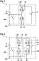
- Figures 3 and 4 show different cell types of the switching cells 1. All switching cells 1 are provided between a first cell terminal 100 and a second cell terminal 200. In figure 3 , a half bridge is shown, while figure 4 shows a full bridge. While the half bridge can block the current in one direction only, the full bridge can block the current in two directions.
- the half bridge design shown in figure 3 therefore is a switching cell 1 using only one single first switching unit 2.
- the switching cell 1 according to the full bridge design shown in figure 4 on the other side has a first switching unit 2 and a second switching unit 3.
- the first switching unit 2 and the second switching unit 3 are half bridge elements. Therefore, the two half bridge elements of the first switching unit 2 and the second switching unit 3 are combined to form a full bridge in figure 4 .
- Each of the switching units 2, 3 therefore has two IGBTs 80 and two diodes 90.
- One IGBT 80 and one diode 90 are connected in parallel and the two sets of parallel IGBT 80 and diode 90 are connected in series. In this way, the above-described half bridge element is formed.
- Each switching cell 1 further includes at least a first capacitor 4.
- the first capacitor 4 is provided in parallel to the switching units 2, 3.
- the switching cells 1 divide the phase output voltage 300 in several cell voltages 400, between the first cell terminal 100 and second cell terminal 200 of the respective switching cell 1, such that the switching cells 1 can be used to convert the phase output voltage 300 to direct voltage.
- a bypass switch 19 may be provided to allow current to bypass the switching cell 1 in case of a cell failure and thus keep the converter 20 operating. This may be realized using a combination of thyristor, mechanical contactor or fast-acting pyrotechnic device.
- the bypass switch 19 may not be required if the semiconductor switch used in the cell fail to short, e.g. specially-designed press-pack IGBTs or integrated gate commutated thyristors (IGCTs).
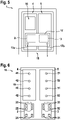
- FIG. 5 is a schematic view of the switching cell 1 according to an embodiment of the invention.
- the switching cell 1 includes a first switching unit 2 and a second switching unit 3 as shown in figures 3 and 4 as well as a first capacitor 4 and a second capacitor 5.
- Figure 5 shows the first switching unit 2, the second switching unit 3, the first capacitor 4 and the second capacitor 5 being mounted on a common chassis 15.
- the two switching units 2, 3 also share the same heat sink 17, such that the switching cell 1 only has a single inlet 17a and outlet 17b for cooling fluid.
- the switching cell 1 also has a common control unit 16, which particularly drives the IGBTs 80 of the switching units 2, 3. Therefore, the switching cell 1 has a higher energy density compared with two single cells only having one switching unit.
- the chassis 15 functions as common chassis ground.
- the switching cell 1 does not have a fixed cell design.
- the switching cell 1 can rather be configured to have different cell designs such that a flexibility in providing a converter 20 with different demands is given.
- the switching cell 1 has a base module 18, which includes the first switching unit 2, the second switching unit 3, the first capacitor 4 and the second capacitor 5.
- the base module 18 is also adapted to receive different busbar sets. Each busbar set connects the elements of the base module 18 in a different manner to realize different cell designs.
- the busbars of the busbar sets contact the elements of the base module 18 all from the same side. Therefore, mounting the busbar sets and electrically connecting the first switching unit 2, the second switching unit 3, the first capacitor 4 and the second capacitor 5 is simplified.
- the first switching unit 2 has a first AC voltage terminal 21, a first negative DC terminal 22, and a first positive DC terminal 23.
- a first switch is provided between the first AC voltage terminal 21 and the first negative DC terminal 22, and a second switch between the first AC voltage terminal 21 and the first positive DC terminal 23, wherein the two switches consist of the above described parallel IGBT 80 and diode 90.
- the second switching unit 3 has a second AC voltage terminal 31, a second negative DC terminal 32, and second positive DC terminal 33.
- a third switch is provided between the second AC voltage terminal 31 and the second negative DC terminal 32, and a fourth switch between the second AC voltage terminal 31 and the second positive DC terminal 33.
- the two switches i.e. the third switch and the fourth switch, consists of the above described parallel IGBT 80 and diode 90.
- the first capacitor 4 is provided between a first capacitor terminal 41 and a second capacitor terminal 42 and the second capacitor 5 is provided between a third capacitor terminal 51 and a fourth capacitor terminal 52. All the terminals described above are preferably on the same side of the switching cell 1 to ensure that the switching cell 1 can be electrically contacted via the busbar sets from a single side.
- the switching cell 1 can be set to different cell designs.
- the two switching units 3, 4 can be paralleled to increase the current rating or to form a full bridge.
- the switching units 3, 4 can also be put in series to form a dual switching cell consisting of two conventional switching cells.
- three different designs are shown which are all realized by different busbar sets with the same base module 18.
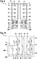
- FIGS 7 and 8 two parallel half bridge circuits between the first cell terminal 100 and the second cell terminal 200 are shown.
- Figure 7 schematically shows the design of the switching cell 1 while figure 8 shows a schematic wire diagram.
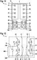
- figures 9 and 10 two serial half bridge circuits between the first cell terminal 100 and the second cell terminal 200 is shown.
- Figure 9 schematically shows the design of the switching cell 1 while figure 10 shows a schematic wire diagram.
- a full bridge circuit between the first cell terminal 100 and the second cell terminal 200 is finally shown in figures 11 and 12.
- Figure 11 schematically shows the design of the switching cell 1, while figure 12 shows a schematic wire diagram.
- a first busbar set including a first busbar 6, a second busbar 7, and a third busbar 8 is used to interconnect the first AC voltage terminal 21, the first negative DC terminal 22, the first positive DC terminal 23, the second AC voltage terminal 31, the second negative DC terminal 32, the second positive DC terminal 33, the first capacitor terminal 41, the second capacitor terminal 42, the third capacitor terminal 51, and the fourth capacitor terminal 52.
- the first negative DC terminal 22 and the second negative DC terminal 32 and the second capacitor terminal 42 and the fourth capacitor terminal 52 are electrically connected via the first busbar 6.
- the first positive DC terminal 23 and the second positive DC terminal 33 and the first capacitor terminal 41 and the third capacitor terminal 51 are electrically connected via the second busbar 7.
- the third busbar 8 electrically connects the first AC voltage terminal 21 and the second AC voltage terminal 31.
- the first busbar 6 is the second cell terminal 200 and the third busbar 8 is the first cell terminal 100.
- the switching cell 1 is a fully-rated half bridge since the parallel connection of components doubles the current the switching cell can carry.
- a common chassis ground is provided via the chassis 15 at the first negative DC terminal 22 and the second negative terminal 23, which are identical in this design.
- the same base module 18 can be provided with a different second busbar set shown in figures 9 and 10 to form a half-rated dual cell.
- the second busbar set includes a fourth busbar 9, a fifth busbar 10, a sixth busbar 11, a seventh busbar 12, and an eighth busbar 13, which interconnect the first AC voltage terminal 21, the first negative DC terminal 22, the first positive DC terminal 23, the second AC voltage terminal 31, the second negative DC terminal 32, the second positive DC terminal 33, the first capacitor terminal 41, the second capacitor terminal 42, the third capacitor terminal 51, and the fourth capacitor terminal 52.
- the first AC voltage terminal 21 is electrically connected to the fourth busbar 9.
- the first positive DC terminal 23 and the first capacitor terminal 41 are electrically connected via the fifth busbar 10.
- the second negative DC terminal 32 and the fourth capacitor terminal 52 are electrically connected via the sixth busbar 11.
- the seventh busbar 12 electrically connects the first negative DC terminal 22 and the second positive DC terminal 33 and the second capacitor terminal 42 and the third capacitor terminal 51.
- the second AC voltage terminal 31 is electrically connected to the eighth busbar 13.
- the fourth busbar 9 is the first cell terminal 100 and the eighth busbar 13 is the second cell terminal 200.
- the first switching unit 2 and the first capacitor 4 form a half-rated half bridge which is connected in series to another half-rated half bridge formed from the second switching unit 3 and the second capacitor 5.
- the two half-rated half bridges are formed as mirror of each other such that they can share the same power supply and controller.
- a common chassis ground is provided by chassis 15 at the first negative DC terminal 22 and the second positive DC terminal which are identical in this design.
- the cell outputs the double cell voltage 500, which is twice the cell voltage 400.
- a fully-rated half bridge or two half-rated half bridges can be provided.
- the same base module 18 can be provided as different cell topologies.
- bypass switch 19 may be used for each of the two half bridges, with the two bypass switches connected in series and the mid-point between them also connected to the mid-point between the two half bridges, or one bypass switch may be used for the whole switching cell 1.
- each one needs the same voltage rating as for the single switching cell 1, while using a single bypass switch for the whole switching cell 1 requires a higher voltage rating since the bypass switch 19 has to carry the double cell voltage 500 which is twice the cell voltage 400.
- Figures 11 and 12 finally show a half-rated full bridge design.
- the two switching units 2, 3, which are formed as half bridge modules, are combined to set up a full bridge.
- a third busbar set including the above-described second busbar 7, the above-described fourth busbar 9, the above-described eighth busbar 13, and an additional ninth busbar 14.
- the ninth busbar 14 electrically connects the first negative DC terminal 22 and the second negative DC terminal 32 and the second capacitor terminal 42 and the fourth capacitor terminal 52.
- the chassis 15 provides a common chassis ground at the first negative DC terminal 22 and the second negative DC terminal 32.
- the busbars of each busbar set advantageously are laminated busbars. This particularly helps to reduce the stray inductance between the IGBTs 80 and the capacitors 4, 5 to ensure optimal switching of the switching cells 1.
- the base module 18 can be provided with another busbar set to form a half-rated full bridge.
- the base module 18 can be provided with another busbar set to form a half-rated full bridge.
- Figure 13 shows the same cell design of the switching cell 1 as shown in figure 7 , wherein a different first switching unit 2 and second switching unit 3 are used.
- the first switching unit 2 and the second switching unit 3 are described as half bridge modules.
- another setup using single switch modules can also be adopted.
- the first switching unit 2 includes a first sub-switching unit 2a and a second sub-switching unit 2b.
- the first sub-switching unit 2a has the first AC voltage terminal 21, the first negative DC terminal 22, and the first switch provided between the first AC voltage terminal 21 and the first negative DC terminal 22.
- the second sub-switching unit 2b also has the first AC voltage terminal 21 and further includes the first positive DC terminal 23, and the second switch provided between the first AC voltage terminal 21 and the first positive DC terminal 23.
- the second switching unit 3 includes a third sub-switching unit 3a and a fourth sub-switching unit 3b.
- the third sub-switching unit 3a has the second AC voltage terminal 31, the second negative DC terminal 32, and the third switch, which is provided between the second AC voltage terminal 31 and the second negative DC terminal 31.
- the fourth sub-switching unit 3b has the second AC voltage terminal 31, the second positive DC terminal 33, and the fourth switch, which is provided between the second AC voltage terminal 31 and the second positive DC terminal 33.
- the sub-switching units 2a, 2b, 3a, 3b have to be contacted separately via the first busbar 6, the second busbar 7, and the third busbar 8, wherein the cell design remains the same as shown in figure 7 .
- the setup of the switching units 2, 3, i.e. the usage of the sub-switching units 2a, 2b, 3a, 3b can be applied to any other cell design, particularly to the designs shown in figure 9 and 11 .
- FIG 14 finally shows a further design option of the switching units 2, 3.
- the switching units 2, 3 are provided as multi-level bridge legs with three levels.
- an additional diode 90 is included in each switching unit 2, 3.
- the switching cell 1 as described above can be used for different purposes, while all switching cells 1 share the same base components. Thus, always the same hardware can be adopted for providing a variety of different switching cells 1 for a convertor 20.
- the switching cells 1 are of lower costs since only one set of control components, e.g. the control unit 16 and the heat sink 17, has to be provided.
- the switching cells 1 are such that a maximum component re-use and design re-use is possible. Further, particularly in the case of the dual cell including two half-rated half bridges, a compact cell design is provided. Since the component count and the number of coolant and electrical connections are reduced, the reliability is increased.
- Reference signs 1 switching cell 100 first cell terminal 2 first switching unit 200 second cell terminal 21 first AC voltage terminal 300 phase output voltage 22 first negative DC terminal 400 cell voltage 23 first positive DC terminal 500 double cell voltage 3 second switching unit 600 three-phase voltage input 31 second AC voltage terminal 32 second negative DC terminal 33 second positive DC terminal 4 first capacitor 41 first capacitor terminal 42 second capacitor terminal 5 second capacitor 51 third capacitor terminal 52 fourth capacitor terminal 6 first busbar 7 second busbar 8 third busbar 9 fourth busbar 10 fifth busbar 11 sixth busbar 12 seventh busbar 13 eighth busbar 14 ninth busbar 15 chassis 16 control unit 17 heat sink 17a inlet 17b outlet 18 base module 19 bypass switch 20 converter unit 80 IGBT 90 Diode
Description
- The invention regards a modular switching cell. Particularly, the switching cell includes a base module, which can be configured by connecting terminals of the base module via pre-shaped busbars in different ways in order to realize different cell module types. The invention further regards a system including said modular switching cell and respective busbars. Finally, the invention regards a method for manufacturing a modular switching cell.
- From the prior art, Multi-level Modular Converter (MMC) are known. The MMC is the standard approach within the power converter industry to realise High Voltage Direct Current (HVDC) converters for use in power transmission. They are being widely adopted, too, for use in medium-voltage (MV) drive applications, including power distribution applications such as STATCOM.
- An MMC converter consists of multiple cells connected in series to form a phase arm; one or two of these may be used per phase, depending on the application. Traditional MMC cells are half-bridge or full-bridge, half-bridge cells block voltage in one direction while full-bridge cells block voltage in both directions. The MMC cells usually include insulated gate bipolar transistors.
- In a family of production converters, there may be a range of overall converter current and voltage ratings, to suit a wide range of applications. Accommodating different voltage ratings is straightforward given that many cells are placed in series to achieve the required voltage rating; however the current rating of the converter typically falls within the current rating of a single cell. Therefore to produce a range of converter current ratings either requires a range of different cell designs, each with a different current rating, or underutilization of the cell current rating for low-current converter designs resulting in a high cost per kW.
- Traditional MMC cell designs are available in the public domain. Many are described in the following publications:
- K. Sharifabadi, L. Harnefors, H-P. Nee, S. Norrga and R. Teodorescu, "Design, Control and Application of Modular Multilevel Converters for HVDC Transmission Systems," John Wiley & Sons/IEE Press, 2016
- M. Merlin, "HVDC activity at Imperial College" 2015, slides 16-18,
- Alstom Grid/GE Grid references: C. Barker, HVDC Plenary Session, IEEE EPEC 2011
- C. Bartzsch, H. Huang, T. Westerweller and M. Davies, "HVDC PLUS and SVC PLUS: Reliable and Cost-effective Power Transmission Solutions with Modular Multilevel Converters," 2011, The problem with the above prior art is that the cell design is highly optimized for a particular topology and current rating. The optimization for a particular current rating affects, for example, the choice of IGBT/diode module, cell capacitor and bypass switch. The current rating is often given as share of a predetermined current value. For example, a fully-rated cell can carry the whole predetermined current. A half-rated cell can only carry half of the predetermined current. While a half-rated cell may theoretically result in half the size, the constituent component availability may preclude this, e.g. if the IGBT module is only available to suit the full cell rating. Even where half-rated cell components are available, each half-rated cell will still require the same quantity of control components, i.e. cell controller, current/voltage sensors, cell power supply, etc., as the fully-rated cell and a similar cost and volume of mechanical components. The rack-support structure for multiple cells will also be different, because of the different size. Therefore a half-rated cell will result in significantly more than half the cost and volume of the fully-rated cell, and hence the resulting MMC converter will be more expensive (€/kW) and less power dense (kW/m3). Furthermore, the half-rated cell will require a separate design, with associated engineering costs.
- This lack of flexibility is also apparent if a full-bridge cell is required. Unless half-rated cell components are available, then a half-rated full-bridge cell will similarly require a separate design, with associated engineering costs.
-
WO2019120468 describes a Modular Multilevel Converter, wherein each phase leg comprises a first cell arrangement comprising a plurality of series-connected converter cells and a second cell arrangement comprising a plurality of series-connected converter cells. The phase leg also comprises a circuit breaker arrangement comprising a plurality of circuit breakers arranged to enable alternately connecting the first and second cell arrangements in series, when the voltage is high, and in parallel, when the current is high, by means of the plurality of circuit breakers. The ability to modularize aids in scalability and redundancy of this converter design. - Furthermore,
CN202616988U describes the assembly of a full-bridge submodule by using two half-bridge submodules with corresponding capacitors. - Therefore, the problem to be solved is finding a switching cell that is cheap, has a high power density and can be used for different topologies and current ratings. This object is solved by the features of the independent claims. The dependent claims contain advantageous embodiments of the invention.
- The invention describes a common cell design which uses the same basic mechanical design for either a fully-rated cell or two series half-rated cells, with the latter resulting in the same cost per until power rating and power density as the fully-rated cell. These could share a mainly common design, simplifying the design effort and resulting in a lower cost system.
- The invention is solved by a modular switching cell of a high voltage direct current power converter, which comprises a base module. The base module has a first switching unit, a second switching unit, a first capacitor, and a second capacitor. These elements, i.e. the first switching unit, the second switching unit, the first capacitor, and the second capacitor are all mounted on a common chassis. In this way, the base module allows for different interconnection of the elements in order to arrive at different designs. The first switching unit and the second switching unit preferably include IGBTs.
- The base module is adapted to receive at least three different busbar sets, each including a plurality of busbars for interconnecting the first switching unit, the second switching unit, the first capacitor, and the second capacitor. Each of the busbar sets allows a different design of the base module. In particular, one of the busbar sets allows forming two parallel half bridge circuits between a first cell terminal and a second cell terminal. In addition, another one of the busbar sets allows forming two serial half bridge circuits between the first cell terminal and the second cell terminal. Yet another one of the busbar sets allows forming a full bridge circuit between the first cell terminal and the second cell terminal. Therefore, each busbar set interconnects the above described elements of the base module in a different manner. Hence, the base module can be used for different cell types, particularly for different current ratings and topologies. Therefore, the modular switching cell is cheap and allows high power densities.
- Therefore, the invention provides a common cell design, which uses the same basic mechanical design, i.e. the base module, for either a fully-rated cell or two series of half-rated cells, with the latter resulting in the same cost per unit power rating and power density as the fully rated cell. These cell types share a manly common design and thereby simplifying the design effort and resulting in a lower cost system.
- Preferably, the first switching unit has a first AC voltage terminal, a first negative DC terminal, a first positive DC terminal, a first switch between the first AC voltage terminal and the first negative DC terminal, and a second switch between the first AC voltage terminal and the first positive DC terminal. In this way, the first switching unit is particularly formed as half bridge module. Further, the second switching unit preferably has a second AC voltage terminal, a second negative DC terminal, a second positive DC terminal, a third switch between the second AC voltage terminal and the second negative DC terminal, and a fourth switch between the second AC voltage terminal and the second positive DC terminal. Again, the second switching unit is particularly formed as half bridge module. The base module is adapted to receive each busbar set such that the busbars of the respective busbar set interconnect all the terminals of the first switching unit and the second switching unit and the first capacitor and the second capacitor. In this way, particularly the first AC voltage terminal, the first negative DC terminal, the first positive DC terminal, the second AC voltage terminal, the second negative DC terminal, the second positive DC terminal, the first capacitor, and the second capacitor are interconnected. The busbars are provided such that they form one of the two parallel half bridge circuits, the two serial half bridge circuits, and the full bridge circuit. Therefore, only the busbars have to be different in case a different circuit has to be provided. Therefore, one basis module can be used for implementing a wide variety of power converters.
- In a preferred embodiment, at least the first negative DC terminal is electrically connected to the chassis. The chassis preferably functions as chassis ground. Depending on the cell design defined by the busbar sets, the second positive DC terminal or the second negative DC terminal are preferably also connected to the chassis. It is preferable that all switching units share the same chassis ground, such that particularly only a single chassis ground potential exists in the modular switching cell.
- Further preferred, the first switch and the second switch of the first switching unit and the third switch and the fourth switch of the second switching unit all include an electronic switch. The electronic switch particularly comprises an insulated-gate bipolar transistor (IGBT), and a diode which are wired in parallel to each other. Instead of IGBTs, also other electronic switches like integrated gate-commutated thyristors (IGCT), gate turn-off thyristors (GTO-Thyristors), metal oxide semiconductor field-effect transistos (MOSFETs), high-electron-mobility transistors (HEMT) or bipolar junction transistors (BJT) can be used. All these elements can be combined in different manners, i.e. via different busbar sets, in order to realize different modular switching cells and thus power converters.
- The modular switching cell preferably includes a single control unit. The control unit is adapted to switch the first switch and the second switch of the first switching unit and the third switch and the fourth switch of the second switching unit. In this way, the power input to the modular switching cell can undergo optimal power conversion. The converted power is output. Thereby, the whole control of all the switches is preferably controlled by the single control unit.
- Further preferred, the first switching unit includes a first sub-switching unit and a second sub-switching unit. In this case, the first switching unit and the second switching unit are not half bridge modules (e.g. half-bridge IGBTs) but rather are single switch modules (e.g. IGBTs). The first sub-switching unit preferably includes the first AC voltage terminal, the first negative DC terminal, and the first switch. The second sub-switching unit preferably includes the first AC voltage terminal, the first positive DC terminal, and the second switch. Thus, the interconnection of the first switching element is still possible via the busbar sets, wherein the two sub-switching units have to be connected separately. In the same way, the second switching unit preferably includes a third sub-switching unit and a fourth sub-switching unit. The third sub-switching unit has the second AC voltage terminal, the second negative DC terminal, and the third switch. The fourth sub-switching unit on the other side has the second AC voltage terminal, the second positive DC terminal, and, the fourth switch. Thus, the second switching unit also includes two sub-switching units, which are to be connected separately via the busbars.
- It is further preferred that a heat sink is provided. The heat sink is particularly provided to dissipated heat of more than one switching unit. Preferably, the first switching unit, the second switching unit, the first capacitor, and the second capacitor are provided with a common heat sink. Therefore, the power density of the cell is improved and the costs for providing the cell is reduced.
- The modular switching cell particularly has a bypass switch provided between the first cell terminal and the second cell terminal. The bypass switch is adapted to bypass the switching cell, by shortcutting the first cell terminal and the second cell terminal. In case a converter is set up of the modular switching cells as described above, the bypass switch allows to not use the respective switching cell, e.g. in case of damage of the switching cell. Thus, failure of one switching cell does not necessarily lead to a failure of the whole converter. In an alternative embodiment, the bypass switch is omitted and the components of the switching cell are adapted to shortcut the first cell terminal and the second cell terminal in case of component failure.
- In another advantageous embodiment, the first switching unit, the second switching unit, the first capacitor, and the second capacitor are electrically connectable via the busbar sets all from the same side. Thus, the busbar set only has to be arranged on one side of the base module to interconnect all the components. Therefore, different cell designs, particularly the cell designs as described above, can be provided in a simplified manner.
- The invention further regards a system including the modular switching cell as described above and at least two of a first busbar set and a second busbar set and a third busbar set. Therefore, the system can be configured to provide different cell designs. A converter can preferably be set up from several of these systems. In the system, the first capacitor is provided between a first capacitor terminal and a second capacitor terminal and the second capacitor is provided between a third capacitor terminal and a fourth capacitor terminal. All these capacitor terminal can be connected via the busbars of the busbar set to connect the switching units and the capacitors. With the different busbar sets, different designs can be provided, wherein these different busbar sets are now described:
The first busbar set includes a first busbar, a second busbar, and a third busbar. The first busbar electrically connects the first negative DC terminal and the second negative DC terminal and the second capacitor terminal and the fourth capacitor terminal. The second busbar electrically connects the first positive DC terminal and the second positive DC terminal and the first capacitor terminal and the third capacitor terminal. Finally, the first AC voltage terminal and the second AC voltage terminal are electrically connected via the third busbar. In this cell design, the first busbar is the second cell terminal and the third busbar is the first cell terminal. Therefore, the first busbar set preferably defines a fully rated half-bridge cell. This means that the switching units are half-rated and are connected in parallel via the first busbar set. Hence, the cell design is a half-bridge, while each switching unit particularly carries half the current flowing through each cell. - In an additional or alternative embodiment, the second busbar set includes a fourth busbar, a fifth busbar, a sixth busbar, a seventh busbar, and an eighth busbar. The fourth busbar is electrically connected to the first AC voltage terminal. The fifth busbar electrically connects the first positive DC terminal and the first capacitor terminal. The second negative DC terminal and the fourth capacitor terminal are electrically connected via the sixth busbar. The seventh busbar electrically connects the first negative DC terminal and the second positive DC terminal and the second capacitor terminal and the third capacitor terminal. Finally, the eighth busbar is electrically connected to the second AC voltage terminal. According to this cell design, the fourth busbar is the first cell terminal and the eighth busbar is the second cell terminal. In this cell design, a half-rated dual cell is provided. This means that the two switching units are connected in series such that the cell fulfils the function of two half-rated cells.
- In another additional or alternative embodiment, the third busbar set includes the second busbar as described before, the fourth busbar as described before, the eighth busbar as described before, and a ninth busbar. The ninth busbar electrically connects the first negative DC terminal and the second negative DC terminal and the second capacitor terminal and the fourth capacitor terminal. This cell design realizes a half-rated full-bridge. Therefore, the switching units are coupled such that they form a full-bridge. Particularly, as described above, each of the switching unit is a half bridge modules, such that these half bridge modules are combined by the third busbar set to form a full-bridge.
- Hence, from the same base module, i.e. from the same switching units and capacitors, at least three different cell designs can be produced only by combining the base module with one of the first busbar set and second busbar set and third busbar set. This allows an increased flexibility in providing different cell types and/or converters.
- The busbars of each busbar set advantageously are laminated busbars. By providing laminated busbars, the required space for interconnecting the switching units and capacitors is reduced. In addition, the electrical properties are enhanced, e.g. the stray inductance is reduced.
- Each busbar set includes busbars that define the first cell terminal and the second cell terminal arranged for electrically connecting the switching cell with other components, particularly with other switching cells of the power converter. Therefore, in order to set up a converter, each cell is connected via the respective busbars forming the cell terminals.
- The invention also regards a high voltage direct current power converter. The converter includes a three phase voltage input and, for each phase of the three phase voltage input, a plurality of switching cells as described above. The switching cells are connected in series. Therefore, the power converter can be provided with flexible and inexpensive switching cells as described above, wherein said switching cells particularly have a high energy density. The invention finally regards a method of manufacturing a modular switching cell. The method comprises the following steps: On the one side, a base module is provided by mounting a first switching unit, a second switching unit, a first capacitor, and a second capacitor on a chassis. This base module is adapted to receive different busbar sets in order to realize different cell designs. Hence, at least three different busbar sets are provided. Each set includes a plurality of busbars for interconnecting the first switching unit, the second switching unit, the first capacitor, and the second capacitor. The busbars of each busbar set are adapted to form one of two parallel half bridge circuits between a first cell terminal and a second cell terminal, and two serial half bridge circuits between the first cell terminal and the second cell terminal, and a full bridge circuit between the first cell terminal and the second cell terminal. Thus, each busbar set allows another cell design by interconnecting the elements of the base module in different manners. As a last step, one of the busbar sets is mounted on the base element. By mounting the respective busbar set on the base element, a switching cell is provided which has one of the designs listed above. Since any one of the bus bar sets can be mounted on the base module, it is a simple and flexible way of providing different switching cell types.
- Further embodiments and advantages will become apparent from the following description of the drawings. In the drawings
- Fig. 1
- is a schematic view of a high voltage direct current power converter according to an embodiment of the present invention,
- Fig. 2
- is a schematic view of a phase output voltage of the high voltage direct current power converter according to the embodiment of the present invention,
- Fig. 3
- is a schematic view of a half-bridge switching cell of the high voltage direct current power converter according to the embodiment of the present invention,
- Fig. 4
- is a schematic view of a full-bridge switching cell of the high voltage direct current power converter according to the embodiment of the present invention,
- Fig. 5
- is a schematic view of a switching cell according to an embodiment of the present invention,
- Fig. 6
- is a schematic view of a base module of the switching cell according to the embodiment of the present invention,
- Fig. 7
- is a schematic view of a first alternative of the switching cell according to the embodiment of the present invention,
- Fig. 8
- is a schematic wire diagram of the first alternative of the switching cell according to the embodiment of the present invention,
- Fig.9
- is a schematic view of a second alternative of the switching cell according to the embodiment of the present invention,
- Fig. 10
- is a schematic wire diagram of the second alternative of the switching cell according to the embodiment of the present invention,
- Fig. 11
- is a schematic view of a third alternative of the switching cell according to the embodiment of the present invention,
- Fig. 12
- is a schematic wire diagram of the third alternative of the switching cell according to the embodiment of the present invention,
- Fig. 13
- is a schematic view of a switching cell according to another embodiment of the invention, and
- Fig. 14
- is a schematic wire diagram of a switching cell in yet another alternative.
-
Fig. 1 is a schematic view of a high voltage directcurrent converter 20, particularly for use in power transmission. The high voltage directcurrent power converter 20 includes a threephase voltage input 600 and is adapted to output direct voltage. For each phase of the threephase voltage input 600, a plurality of switchingcells 1 are connected in series. Aphase output voltage 300 can thus be divided into a plurality ofcell voltages 400 of thesingle switching cells 1 as shown infigure 2 . By respective switching of theswitching cells 1, thephase output voltage 300 can be converted to direct voltage. -
Figures 3 and 4 show different cell types of theswitching cells 1. All switchingcells 1 are provided between afirst cell terminal 100 and asecond cell terminal 200. Infigure 3 , a half bridge is shown, whilefigure 4 shows a full bridge. While the half bridge can block the current in one direction only, the full bridge can block the current in two directions. The half bridge design shown infigure 3 therefore is a switchingcell 1 using only one singlefirst switching unit 2. The switchingcell 1 according to the full bridge design shown infigure 4 on the other side has afirst switching unit 2 and asecond switching unit 3. In this embodiment, thefirst switching unit 2 and thesecond switching unit 3 are half bridge elements. Therefore, the two half bridge elements of thefirst switching unit 2 and thesecond switching unit 3 are combined to form a full bridge infigure 4 . - Each of the switching
units IGBTs 80 and twodiodes 90. OneIGBT 80 and onediode 90 are connected in parallel and the two sets ofparallel IGBT 80 anddiode 90 are connected in series. In this way, the above-described half bridge element is formed. - Each switching
cell 1 further includes at least afirst capacitor 4. Thefirst capacitor 4 is provided in parallel to theswitching units cells 1 divide thephase output voltage 300 inseveral cell voltages 400, between thefirst cell terminal 100 andsecond cell terminal 200 of therespective switching cell 1, such that the switchingcells 1 can be used to convert thephase output voltage 300 to direct voltage. - A
bypass switch 19 may be provided to allow current to bypass the switchingcell 1 in case of a cell failure and thus keep theconverter 20 operating. This may be realized using a combination of thyristor, mechanical contactor or fast-acting pyrotechnic device. Thebypass switch 19 may not be required if the semiconductor switch used in the cell fail to short, e.g. specially-designed press-pack IGBTs or integrated gate commutated thyristors (IGCTs). -
Figure 5 is a schematic view of the switchingcell 1 according to an embodiment of the invention. The switchingcell 1 includes afirst switching unit 2 and asecond switching unit 3 as shown infigures 3 and 4 as well as afirst capacitor 4 and asecond capacitor 5.Figure 5 shows thefirst switching unit 2, thesecond switching unit 3, thefirst capacitor 4 and thesecond capacitor 5 being mounted on acommon chassis 15. The twoswitching units same heat sink 17, such that the switchingcell 1 only has asingle inlet 17a andoutlet 17b for cooling fluid. The switchingcell 1 also has acommon control unit 16, which particularly drives theIGBTs 80 of the switchingunits cell 1 has a higher energy density compared with two single cells only having one switching unit. In addition, since all the components are provided on thesame chassis 15, thechassis 15 functions as common chassis ground. - The switching
cell 1 does not have a fixed cell design. The switchingcell 1 can rather be configured to have different cell designs such that a flexibility in providing aconverter 20 with different demands is given. To allow different cell designs, the switchingcell 1 has abase module 18, which includes thefirst switching unit 2, thesecond switching unit 3, thefirst capacitor 4 and thesecond capacitor 5. Thebase module 18 is also adapted to receive different busbar sets. Each busbar set connects the elements of thebase module 18 in a different manner to realize different cell designs. - Preferably, the busbars of the busbar sets contact the elements of the
base module 18 all from the same side. Therefore, mounting the busbar sets and electrically connecting thefirst switching unit 2, thesecond switching unit 3, thefirst capacitor 4 and thesecond capacitor 5 is simplified. - In order to be electrically contacted by the busbar sets, the
first switching unit 2 has a firstAC voltage terminal 21, a firstnegative DC terminal 22, and a firstpositive DC terminal 23. A first switch is provided between the firstAC voltage terminal 21 and the firstnegative DC terminal 22, and a second switch between the firstAC voltage terminal 21 and the firstpositive DC terminal 23, wherein the two switches consist of the above describedparallel IGBT 80 anddiode 90. - In the same way, the
second switching unit 3 has a secondAC voltage terminal 31, a secondnegative DC terminal 32, and secondpositive DC terminal 33. A third switch is provided between the secondAC voltage terminal 31 and the secondnegative DC terminal 32, and a fourth switch between the secondAC voltage terminal 31 and the secondpositive DC terminal 33. Again, the two switches, i.e. the third switch and the fourth switch, consists of the above describedparallel IGBT 80 anddiode 90. - The
first capacitor 4 is provided between afirst capacitor terminal 41 and asecond capacitor terminal 42 and thesecond capacitor 5 is provided between athird capacitor terminal 51 and afourth capacitor terminal 52. All the terminals described above are preferably on the same side of the switchingcell 1 to ensure that the switchingcell 1 can be electrically contacted via the busbar sets from a single side. - Starting from such a basic design, the switching
cell 1 can be set to different cell designs. Particularly, the two switchingunits units same base module 18. - In
figures 7 and 8 , two parallel half bridge circuits between thefirst cell terminal 100 and thesecond cell terminal 200 are shown.Figure 7 schematically shows the design of the switchingcell 1, whilefigure 8 shows a schematic wire diagram. Infigures 9 and 10 , two serial half bridge circuits between thefirst cell terminal 100 and thesecond cell terminal 200 is shown.Figure 9 schematically shows the design of the switchingcell 1, whilefigure 10 shows a schematic wire diagram. A full bridge circuit between thefirst cell terminal 100 and thesecond cell terminal 200 is finally shown infigures 11 and 12. Figure 11 schematically shows the design of the switchingcell 1, whilefigure 12 shows a schematic wire diagram. - In the design according to
figures 7 and 8 , a first busbar set including afirst busbar 6, asecond busbar 7, and athird busbar 8 is used to interconnect the firstAC voltage terminal 21, the firstnegative DC terminal 22, the firstpositive DC terminal 23, the secondAC voltage terminal 31, the secondnegative DC terminal 32, the secondpositive DC terminal 33, thefirst capacitor terminal 41, thesecond capacitor terminal 42, thethird capacitor terminal 51, and thefourth capacitor terminal 52. - The first
negative DC terminal 22 and the secondnegative DC terminal 32 and thesecond capacitor terminal 42 and thefourth capacitor terminal 52 are electrically connected via thefirst busbar 6. The firstpositive DC terminal 23 and the secondpositive DC terminal 33 and thefirst capacitor terminal 41 and thethird capacitor terminal 51 are electrically connected via thesecond busbar 7. Thethird busbar 8 electrically connects the firstAC voltage terminal 21 and the secondAC voltage terminal 31. In this design, thefirst busbar 6 is thesecond cell terminal 200 and thethird busbar 8 is thefirst cell terminal 100. - As particularly shown in
figure 8 , thefirst switching unit 2, thesecond switching unit 3 as well as thefirst capacitor 4 and thesecond capacitor 5 are connected in parallel to each other. Therefore, the switchingcell 1 is a fully-rated half bridge since the parallel connection of components doubles the current the switching cell can carry. A common chassis ground is provided via thechassis 15 at the firstnegative DC terminal 22 and the secondnegative terminal 23, which are identical in this design. - The
same base module 18 can be provided with a different second busbar set shown infigures 9 and 10 to form a half-rated dual cell. The second busbar set includes afourth busbar 9, afifth busbar 10, asixth busbar 11, aseventh busbar 12, and aneighth busbar 13, which interconnect the firstAC voltage terminal 21, the firstnegative DC terminal 22, the firstpositive DC terminal 23, the secondAC voltage terminal 31, the secondnegative DC terminal 32, the secondpositive DC terminal 33, thefirst capacitor terminal 41, thesecond capacitor terminal 42, thethird capacitor terminal 51, and thefourth capacitor terminal 52. - The first
AC voltage terminal 21 is electrically connected to thefourth busbar 9. The firstpositive DC terminal 23 and thefirst capacitor terminal 41 are electrically connected via thefifth busbar 10. The secondnegative DC terminal 32 and thefourth capacitor terminal 52 are electrically connected via thesixth busbar 11. Theseventh busbar 12 electrically connects the firstnegative DC terminal 22 and the secondpositive DC terminal 33 and thesecond capacitor terminal 42 and thethird capacitor terminal 51. Finally, the secondAC voltage terminal 31 is electrically connected to theeighth busbar 13. In this cell design, thefourth busbar 9 is thefirst cell terminal 100 and theeighth busbar 13 is thesecond cell terminal 200. Thus, thefirst switching unit 2 and thefirst capacitor 4 form a half-rated half bridge which is connected in series to another half-rated half bridge formed from thesecond switching unit 3 and thesecond capacitor 5. Particularly, the two half-rated half bridges are formed as mirror of each other such that they can share the same power supply and controller. A common chassis ground is provided bychassis 15 at the firstnegative DC terminal 22 and the second positive DC terminal which are identical in this design. - In the design of
figures 9 and 10 , the cell outputs thedouble cell voltage 500, which is twice thecell voltage 400. Thus, with the same components, either a fully-rated half bridge or two half-rated half bridges can be provided. Hence, based on the respective needs of theconverter 20, thesame base module 18 can be provided as different cell topologies. - Further, in the design of
figures 9 and 10 , two options apply to thebypass switch 19. Either one bypass switch may be used for each of the two half bridges, with the two bypass switches connected in series and the mid-point between them also connected to the mid-point between the two half bridges, or one bypass switch may be used for thewhole switching cell 1. In case two bypass switches are used, each one needs the same voltage rating as for thesingle switching cell 1, while using a single bypass switch for thewhole switching cell 1 requires a higher voltage rating since thebypass switch 19 has to carry thedouble cell voltage 500 which is twice thecell voltage 400. -
Figures 11 and 12 finally show a half-rated full bridge design. In this design, the two switchingunits second busbar 7, the above-describedfourth busbar 9, the above-describedeighth busbar 13, and an additionalninth busbar 14. Theninth busbar 14 electrically connects the firstnegative DC terminal 22 and the secondnegative DC terminal 32 and thesecond capacitor terminal 42 and thefourth capacitor terminal 52. Thechassis 15 provides a common chassis ground at the firstnegative DC terminal 22 and the secondnegative DC terminal 32. - The busbars of each busbar set advantageously are laminated busbars. This particularly helps to reduce the stray inductance between the
IGBTs 80 and thecapacitors switching cells 1. - Hence, in addition to the fully-rated half bridge and the dual half-rated half bridges, the
base module 18 can be provided with another busbar set to form a half-rated full bridge. Thus there is a wide variety of different cell options which can be provided from onesingle base module 18. -
Figure 13 shows the same cell design of the switchingcell 1 as shown infigure 7 , wherein a differentfirst switching unit 2 andsecond switching unit 3 are used. In the above described embodiments, thefirst switching unit 2 and thesecond switching unit 3 are described as half bridge modules. As shown infigure 13 , another setup using single switch modules can also be adopted. - Thus, the
first switching unit 2 includes a firstsub-switching unit 2a and a secondsub-switching unit 2b. The firstsub-switching unit 2a has the firstAC voltage terminal 21, the firstnegative DC terminal 22, and the first switch provided between the firstAC voltage terminal 21 and the firstnegative DC terminal 22. The secondsub-switching unit 2b also has the firstAC voltage terminal 21 and further includes the firstpositive DC terminal 23, and the second switch provided between the firstAC voltage terminal 21 and the firstpositive DC terminal 23. In an analogous manner, thesecond switching unit 3 includes a thirdsub-switching unit 3a and a fourthsub-switching unit 3b. The thirdsub-switching unit 3a has the secondAC voltage terminal 31, the secondnegative DC terminal 32, and the third switch, which is provided between the secondAC voltage terminal 31 and the secondnegative DC terminal 31. The fourthsub-switching unit 3b has the secondAC voltage terminal 31, the secondpositive DC terminal 33, and the fourth switch, which is provided between the secondAC voltage terminal 31 and the secondpositive DC terminal 33. Thus thesub-switching units first busbar 6, thesecond busbar 7, and thethird busbar 8, wherein the cell design remains the same as shown infigure 7 . The setup of the switchingunits sub-switching units figure 9 and11 . -
Figure 14 finally shows a further design option of the switchingunits units additional diode 90 is included in each switchingunit - In summary, the switching
cell 1 as described above can be used for different purposes, while all switchingcells 1 share the same base components. Thus, always the same hardware can be adopted for providing a variety ofdifferent switching cells 1 for aconvertor 20. The switchingcells 1 are of lower costs since only one set of control components, e.g. thecontrol unit 16 and theheat sink 17, has to be provided. The switchingcells 1 are such that a maximum component re-use and design re-use is possible. Further, particularly in the case of the dual cell including two half-rated half bridges, a compact cell design is provided. Since the component count and the number of coolant and electrical connections are reduced, the reliability is increased.Reference signs 1 switching cell 100 first cell terminal 2 first switching unit 200 second cell terminal 21 first AC voltage terminal 300 phase output voltage 22 first negative DC terminal 400 cell voltage 23 first positive DC terminal 500 double cell voltage 3 second switching unit 600 three- phase voltage input 31 second AC voltage terminal 32 second negative DC terminal 33 second positive DC terminal 4 first capacitor 41 first capacitor terminal 42 second capacitor terminal 5 second capacitor 51 third capacitor terminal 52 fourth capacitor terminal 6 first busbar 7 second busbar 8 third busbar 9 fourth busbar 10 fifth busbar 11 sixth busbar 12 seventh busbar 13 eighth busbar 14 ninth busbar 15 chassis 16 control unit 17 heat sink 17a inlet 17b outlet 18 base module 19 bypass switch 20 converter unit 80 IGBT 90 Diode
Claims (14)
- Modular switching cell (1) of a high voltage direct current power converter (20), comprising a base module (18) with• a first switching unit (2),• a second switching unit (3),• a first capacitor (4), and• a second capacitor (5),characterized in thatthe first switching unit (2), the second switching unit (3), the first capacitor (4), and the second capacitor (5) are mounted on a common chassis (15),wherein the base module (18) is adapted to receive at least three different busbar sets, each including a plurality of busbars (6, 7, 8, 9, 10, 11, 12, 13, 14) for interconnecting the first switching unit (2), the second switching unit (3), the first capacitor (4), and the second capacitor (5) to form one of• two parallel half bridge circuits between a first cell terminal (100) and a second cell terminal (200), and• two serial half bridge circuits between the first cell terminal (100) and the second cell terminal (200), and• a full bridge circuit between the first cell terminal (100) and the second cell terminal (200),wherein the busbar sets are configured to realize different cell designs by using the same base module for either a fully-rated cell being configured to carry a whole predetermined current, or two series half-rated cells being configured to carry half of the predetermined current.
- Modular switching cell (1) according to claim 1, characterized in that• the first switching unit (2) has a first AC voltage terminal (21), a first negative DC terminal (22), a first positive DC terminal (23), a first switch between the first AC voltage terminal (21) and the first negative DC terminal (22), and a second switch between the first AC voltage terminal (21) and the first positive DC terminal (23),• the second switching unit (3) has a second AC voltage terminal (31), a second negative DC terminal (32), a second positive DC terminal (33), a third switch between the second AC voltage terminal (31) and the second negative DC terminal (32), and a fourth switch between the second AC voltage terminal (31) and the second positive DC terminal (33), and• the base module (18) is adapted to receive each busbar set such that the busbars (6, 7, 8, 9, 10, 11, 12, 13, 14) of the respective busbar set interconnect the first AC voltage terminal (21), the first negative DC terminal (22), the first positive DC terminal (23), the second AC voltage terminal (31), the second negative DC terminal (32), the second positive DC terminal (33), the first capacitor (4), and the second capacitor (5) to form one of the two parallel half bridge circuits, the two serial half bridge circuits, and the full bridge circuit.
- Modular switching cell (1) according to claim 2, characterized in that at least the first negative DC terminal (22) is electrically connected to the chassis (15), wherein the chassis (15) functions as chassis ground.
- Modular switching cell (1) according to claim 2 or 3, characterized in that the first switch and the second switch of the first switching unit (2) and the third switch and the fourth switch of the second switching unit (3) all include an electronic switch, particularly an insulated-gate bipolar transistor (80), and a diode (90) which are wired in parallel to each other.
- Modular switching cell (1) according to any one of the claims 2 to 4, characterized by a single control unit (16) adapted to switch the first switch and the second switch of the first switching unit (2) and the third switch and the fourth switch of the second switching unit (3).
- Modular switching cell (1) according to any one of the claims 2 to 5, characterized in that• the first switching unit (2) includes a first sub-switching unit (2a) and a second sub-switching unit (2b),∘ the first sub-switching unit (2a) including the first AC voltage terminal (21), the first negative DC terminal (22), and the first switch, and∘ the second sub-switching unit (2b) including the first AC voltage terminal (21), the first positive DC terminal (23), and the second switch, and• the second switching unit (3) includes a third sub-switching unit (3a) and a fourth sub-switching unit (3b),∘ the third sub-switching unit (3a) including the second AC voltage terminal (31), the second negative DC terminal (32), and the third switch, and∘ the fourth sub-switching unit (3b) including the second AC voltage terminal (31), the second positive DC terminal (33), and the fourth switch.
- Modular switching cell (1) according to any one of the previous claims characterized in that the first switching unit (2), the second switching unit (3), the first capacitor (4), and the second capacitor (5) are provided with a common heat sink (17).
- Modular switching cell (1) according to any one of the previous claims characterized by a bypass switch (19) provided between the first cell terminal (100) and the second cell terminal (200), wherein the bypass switch (19) is adapted to bypass the switching cell (1).
- Modular switching cell (1) according to any one of the previous claims characterized in that the first switching unit (2), the second switching unit (3), the first capacitor (4), and the second capacitor (5), are electrically connectable via the busbar sets all from the same side.
- System including the modular switching cell (1) according any one of claims 2 to 9 and at least two of a first busbar set and a second busbar set and a third busbar set, wherein the first capacitor (4) is provided between a first capacitor terminal (41) and a second capacitor terminal and the second capacitor (5) is provided between a third capacitor terminal (51) and a fourth capacitor terminal (52), wherein• the first busbar set includes a first busbar (6), a second busbar (7), and a third busbar (8), wherein∘ the first negative DC terminal (22) and the second negative DC terminal (32) and the second capacitor terminal (42) and the fourth capacitor terminal (52) are electrically connected via the first busbar (6),∘ the first positive DC terminal (23) and the second positive DC terminal (33) and the first capacitor terminal (41) and the third capacitor terminal (51) are electrically connected via the second busbar (7), and∘ the first AC voltage terminal (21) and the second AC voltage terminal (31) are electrically connected via the third busbar (8),∘ the first busbar (6) is the second cell terminal (200) and the third busbar (8) is the first cell terminal (100),and/or• the second busbar set includes a fourth busbar (9), a fifth busbar (10), a sixth busbar (11), a seventh busbar (12), and an eighth busbar (13), wherein∘ the first AC voltage terminal (21) is electrically connected to the fourth busbar (9),∘ the first positive DC terminal (23) and the first capacitor terminal (41) are electrically connected via the fifth busbar (10),∘ the second negative DC terminal (32) and the fourth capacitor terminal (52) are electrically connected via the sixth busbar (11),∘ the first negative DC terminal (22) and the second positive DC terminal (33) and the second capacitor terminal (42) and the third capacitor terminal (51) are electrically connected via the seventh busbar (12),∘ the second AC voltage terminal (31) is electrically connected to the eighth busbar (13), and∘ the fourth busbar (9) is the first cell terminal (100) and the eighth busbar (13) is the second cell terminal (200),and/or• the third busbar set includes the second busbar (7), the fourth busbar (9), the eighth busbar (13), and a ninth busbar (14) wherein∘ the first negative DC terminal (22) and the second negative DC terminal (32) and the second capacitor terminal (42) and the fourth capacitor terminal (52) are electrically connected via ninth busbar (14).
- System according claim 10 characterized in that the busbars (6, 7, 8, 9, 10, 11, 12, 13, 14) of each busbar set are laminated busbars.
- System according claim 10 or 11 characterized in that each busbar set includes busbars (6, 7, 8, 9, 10, 11, 12, 13, 14) that define the first cell terminal (100) and the second cell terminal (200) arranged for electrically connecting the switching cell (1) with other components, particularly with other switching cells (1), of the power converter (20).
- High voltage direct current power converter (20) including a three phase voltage input (600) and, for each phase of the three phase voltage input (600), a plurality of switching cells (1) according to any one of claims 1 to 9, wherein the switching cells (1) are connected in series.
- Method of manufacturing a modular switching cell (1), characterized by the steps:• providing a base module (18) by mounting a first switching unit (2), a second switching unit (3), a first capacitor (4), and a second capacitor (5) on a common chassis (15).• providing at least three different busbar sets, each including a plurality of busbars (6, 7, 8, 9, 10, 11, 12, 13, 14) for interconnecting the first switching unit (2), the second switching unit (3), the first capacitor (4), and the second capacitor (5), wherein the busbars (6, 7, 8, 9, 10, 11, 12, 13, 14) of each busbar set is adapted to form one of∘ two parallel half bridge circuits between a first cell terminal (100) and a second cell terminal (200), and∘ two serial half bridge circuits between the first cell terminal (100) and the second cell terminal (200), and∘ a full bridge circuit between the first cell terminal (100) and the second cell terminal (200), and• mounting one of the busbar sets on the base element (18),wherein the busbar sets are configured to realize different cell designs by using the same base module for either a fully-rated cell being configured to carry a whole predetermined current, or two series half-rated cells being configured to carry half of the predetermined current.
Priority Applications (6)
| Application Number | Priority Date | Filing Date | Title |
|---|---|---|---|
| EP19197834.5A EP3796539B1 (en) | 2019-09-17 | 2019-09-17 | Modular switching cell |
| KR1020227008978A KR20220061989A (en) | 2019-09-17 | 2020-08-27 | Modular Switching Cell |
| JP2022516324A JP2022548601A (en) | 2019-09-17 | 2020-08-27 | modular switching cell |
| PCT/EP2020/073922 WO2021052730A1 (en) | 2019-09-17 | 2020-08-27 | Modular switching cell |
| CN202080062972.7A CN114342241A (en) | 2019-09-17 | 2020-08-27 | Modular switch unit |
| US17/641,824 US20240048063A1 (en) | 2019-09-17 | 2020-08-27 | Modular switching cell |
Applications Claiming Priority (1)
| Application Number | Priority Date | Filing Date | Title |
|---|---|---|---|
| EP19197834.5A EP3796539B1 (en) | 2019-09-17 | 2019-09-17 | Modular switching cell |
Publications (2)
| Publication Number | Publication Date |
|---|---|
| EP3796539A1 EP3796539A1 (en) | 2021-03-24 |
| EP3796539B1 true EP3796539B1 (en) | 2022-11-23 |
Family
ID=67997378
Family Applications (1)
| Application Number | Title | Priority Date | Filing Date |
|---|---|---|---|
| EP19197834.5A Active EP3796539B1 (en) | 2019-09-17 | 2019-09-17 | Modular switching cell |
Country Status (6)
| Country | Link |
|---|---|
| US (1) | US20240048063A1 (en) |
| EP (1) | EP3796539B1 (en) |
| JP (1) | JP2022548601A (en) |
| KR (1) | KR20220061989A (en) |
| CN (1) | CN114342241A (en) |
| WO (1) | WO2021052730A1 (en) |
Citations (9)
| Publication number | Priority date | Publication date | Assignee | Title |
|---|---|---|---|---|
| EP2254228A1 (en) | 2009-05-20 | 2010-11-24 | ABB Schweiz AG | Electronic switching module and system with such switching modules |
| CN202616988U (en) | 2012-05-03 | 2012-12-19 | Abb研究有限公司 | Half-bridge power converter unit with bypass function |
| CN103441691A (en) | 2013-07-19 | 2013-12-11 | 浙江大学 | Resonance-type power electronic current transformer and current transformer device |
| WO2015131931A1 (en) | 2014-03-05 | 2015-09-11 | Abb Technology Ltd | Multilevel converter |
| WO2018028778A1 (en) | 2016-08-10 | 2018-02-15 | Siemens Aktiengesellschaft | Multilevel converter |
| CN207339661U (en) | 2017-11-13 | 2018-05-08 | 苏州华电电气股份有限公司 | Parallel variable frequency pulse width modulated square wave resonant power |
| JP6345379B1 (en) | 2017-08-09 | 2018-06-20 | 三菱電機株式会社 | Power converter |
| WO2019120468A1 (en) | 2017-12-18 | 2019-06-27 | Abb Schweiz Ag | Mmc phase leg and method for control thereof |
| CN109995258A (en) | 2019-05-15 | 2019-07-09 | 重庆大学 | A kind of inverse-impedance type diode clamp bit submodule and its fault current blocking-up method |
Family Cites Families (4)
| Publication number | Priority date | Publication date | Assignee | Title |
|---|---|---|---|---|
| US7248483B2 (en) * | 2004-08-19 | 2007-07-24 | Xantrex Technology, Inc. | High power density insulated metal substrate based power converter assembly with very low BUS impedance |
| DE102006004031B3 (en) * | 2006-01-27 | 2007-03-08 | Infineon Technologies Ag | Power semiconductor module for inverter etc., has connection points for low and high potentials in sequence that corresponds to that of external connection terminals on two bus rails |
| EP3211784B1 (en) * | 2016-02-25 | 2021-03-31 | GE Energy Power Conversion Technology Ltd | Double submodule for a modular multilevel converter and modular multilevel converter comprising same |
| DE102017221085B4 (en) * | 2017-11-24 | 2020-02-13 | Fraunhofer-Gesellschaft zur Förderung der angewandten Forschung e.V. | Converter circuit |
-
2019
- 2019-09-17 EP EP19197834.5A patent/EP3796539B1/en active Active
-
2020
- 2020-08-27 KR KR1020227008978A patent/KR20220061989A/en unknown
- 2020-08-27 WO PCT/EP2020/073922 patent/WO2021052730A1/en active Application Filing
- 2020-08-27 JP JP2022516324A patent/JP2022548601A/en active Pending
- 2020-08-27 CN CN202080062972.7A patent/CN114342241A/en active Pending
- 2020-08-27 US US17/641,824 patent/US20240048063A1/en active Pending
Patent Citations (9)
| Publication number | Priority date | Publication date | Assignee | Title |
|---|---|---|---|---|
| EP2254228A1 (en) | 2009-05-20 | 2010-11-24 | ABB Schweiz AG | Electronic switching module and system with such switching modules |
| CN202616988U (en) | 2012-05-03 | 2012-12-19 | Abb研究有限公司 | Half-bridge power converter unit with bypass function |
| CN103441691A (en) | 2013-07-19 | 2013-12-11 | 浙江大学 | Resonance-type power electronic current transformer and current transformer device |
| WO2015131931A1 (en) | 2014-03-05 | 2015-09-11 | Abb Technology Ltd | Multilevel converter |
| WO2018028778A1 (en) | 2016-08-10 | 2018-02-15 | Siemens Aktiengesellschaft | Multilevel converter |
| JP6345379B1 (en) | 2017-08-09 | 2018-06-20 | 三菱電機株式会社 | Power converter |
| CN207339661U (en) | 2017-11-13 | 2018-05-08 | 苏州华电电气股份有限公司 | Parallel variable frequency pulse width modulated square wave resonant power |
| WO2019120468A1 (en) | 2017-12-18 | 2019-06-27 | Abb Schweiz Ag | Mmc phase leg and method for control thereof |
| CN109995258A (en) | 2019-05-15 | 2019-07-09 | 重庆大学 | A kind of inverse-impedance type diode clamp bit submodule and its fault current blocking-up method |
Non-Patent Citations (3)
| Title |
|---|
| "Power Electronics", ABB REVIEW - THE CORPORATE TECHNICAL JOURNAL OF THE ABB GROUP, 1 March 2008 (2008-03-01), pages 1 - 80, XP093115792 |
| ALLOCCO J. M.: "LAMINATED BUS BARS FOR POWER SYSTEM INTERCONNECTS.", APEC '97. TWELTH ANNUAL APPLIED POWER ELECTRONICS CONFERENCE AND EXPOSITION. ATLANTA, FEB. 23 - 27, 1997., NEW YORK, IEEE., US, vol. CONF. 12, 23 February 1997 (1997-02-23), US , pages 585 - 589., XP000731005, ISBN: 978-0-7803-3705-3 |
| SMIRNOVA LIUDMILA: "ELECTROMAGNETIC AND THERMAL DESIGN OF A MULTILEVEL CONVERTER WITH HIGH POWER DENSITY AND RELIABILITY", THESIS LAPPEENRANTA UNIVERSITY OF TECHNOLOGY, 1 January 2015 (2015-01-01), pages 1 - 131, XP093115790 |
Also Published As
| Publication number | Publication date |
|---|---|
| KR20220061989A (en) | 2022-05-13 |
| CN114342241A (en) | 2022-04-12 |
| US20240048063A1 (en) | 2024-02-08 |
| JP2022548601A (en) | 2022-11-21 |
| WO2021052730A1 (en) | 2021-03-25 |
| EP3796539A1 (en) | 2021-03-24 |
Similar Documents
| Publication | Publication Date | Title |
|---|---|---|
| Nami et al. | Five level cross connected cell for cascaded converters | |
| US11108338B2 (en) | Dual submodule for a modular multilevel converter and modular multilevel converter including the same | |
| JP6164667B2 (en) | Power conversion circuit and device | |
| US9525348B1 (en) | Power converter having integrated capacitor-blocked transistor cells | |
| KR20160060725A (en) | A new four-level converter cell topology for cascaded modular multilevel converters | |
| WO2007113979A1 (en) | Power converter and its assembling method | |
| WO2012163841A1 (en) | A voltage source converter for a hvdc transmission system | |
| EP3381117B1 (en) | Four-level power converter | |
| US10211642B2 (en) | Electric-power converting device, solar power conditioner system, electricity storage system, uninterruptible power source system, wind power generation system, and motor drive system | |
| KR20090126993A (en) | Multilevel converter consisting of building-block module having power regeneration capability | |
| JP6345361B2 (en) | Power semiconductor module | |
| US10164519B2 (en) | Semiconductor stack for converter with snubber capacitors | |
| US20140167508A1 (en) | Voltage source current controlled multilevel power converter | |
| EP2730018B1 (en) | Integrated boost / 3-level inverter for grid coupling of dc sources, power generation plant and operating method | |
| WO2020059880A1 (en) | Ac voltage output system, power system control system, power system, dc power transmission system, power generation system, and battery system | |
| EP3796539B1 (en) | Modular switching cell | |
| EP3462594B1 (en) | Five-level converter | |
| US20210143750A1 (en) | Modular Inverter | |
| EP3806303A1 (en) | Alternating capacitor step-down dc/dc converter | |
| JP2015089185A (en) | Three-level power conversion device | |
| US11777420B2 (en) | Submodule as a parallel serial full bridge for a modular multilevel converter | |
| Kragl et al. | Battery Inverter System for Stationary, 1500 V Hybrid Battery Storage Applications | |
| WO2018130408A1 (en) | Power module with optimized pin layout | |
| US20230208315A1 (en) | Submodule as a hybrid cell for a modular multilevel converter |
Legal Events
| Date | Code | Title | Description |
|---|---|---|---|
| PUAI | Public reference made under article 153(3) epc to a published international application that has entered the european phase |
Free format text: ORIGINAL CODE: 0009012 |
|
| STAA | Information on the status of an ep patent application or granted ep patent |
Free format text: STATUS: THE APPLICATION HAS BEEN PUBLISHED |
|
| AK | Designated contracting states |
Kind code of ref document: A1 Designated state(s): AL AT BE BG CH CY CZ DE DK EE ES FI FR GB GR HR HU IE IS IT LI LT LU LV MC MK MT NL NO PL PT RO RS SE SI SK SM TR |
|
| AX | Request for extension of the european patent |
Extension state: BA ME |
|
| STAA | Information on the status of an ep patent application or granted ep patent |
Free format text: STATUS: REQUEST FOR EXAMINATION WAS MADE |
|
| 17P | Request for examination filed |
Effective date: 20210924 |
|
| RBV | Designated contracting states (corrected) |
Designated state(s): AL AT BE BG CH CY CZ DE DK EE ES FI FR GB GR HR HU IE IS IT LI LT LU LV MC MK MT NL NO PL PT RO RS SE SI SK SM TR |
|
| GRAP | Despatch of communication of intention to grant a patent |
Free format text: ORIGINAL CODE: EPIDOSNIGR1 |
|
| STAA | Information on the status of an ep patent application or granted ep patent |
Free format text: STATUS: GRANT OF PATENT IS INTENDED |
|
| INTG | Intention to grant announced |
Effective date: 20220719 |
|
| GRAS | Grant fee paid |
Free format text: ORIGINAL CODE: EPIDOSNIGR3 |
|
| GRAA | (expected) grant |
Free format text: ORIGINAL CODE: 0009210 |
|
| STAA | Information on the status of an ep patent application or granted ep patent |
Free format text: STATUS: THE PATENT HAS BEEN GRANTED |
|
| AK | Designated contracting states |
Kind code of ref document: B1 Designated state(s): AL AT BE BG CH CY CZ DE DK EE ES FI FR GB GR HR HU IE IS IT LI LT LU LV MC MK MT NL NO PL PT RO RS SE SI SK SM TR |
|
| REG | Reference to a national code |
Ref country code: GB Ref legal event code: FG4D |
|
| REG | Reference to a national code |
Ref country code: CH Ref legal event code: EP |
|
| REG | Reference to a national code |
Ref country code: AT Ref legal event code: REF Ref document number: 1533766 Country of ref document: AT Kind code of ref document: T Effective date: 20221215 Ref country code: DE Ref legal event code: R096 Ref document number: 602019022163 Country of ref document: DE |
|
| REG | Reference to a national code |
Ref country code: IE Ref legal event code: FG4D |
|
| REG | Reference to a national code |
Ref country code: LT Ref legal event code: MG9D |
|
| REG | Reference to a national code |
Ref country code: NL Ref legal event code: MP Effective date: 20221123 |
|
| REG | Reference to a national code |
Ref country code: AT Ref legal event code: MK05 Ref document number: 1533766 Country of ref document: AT Kind code of ref document: T Effective date: 20221123 |
|
| PG25 | Lapsed in a contracting state [announced via postgrant information from national office to epo] |
Ref country code: SE Free format text: LAPSE BECAUSE OF FAILURE TO SUBMIT A TRANSLATION OF THE DESCRIPTION OR TO PAY THE FEE WITHIN THE PRESCRIBED TIME-LIMIT Effective date: 20221123 Ref country code: PT Free format text: LAPSE BECAUSE OF FAILURE TO SUBMIT A TRANSLATION OF THE DESCRIPTION OR TO PAY THE FEE WITHIN THE PRESCRIBED TIME-LIMIT Effective date: 20230323 Ref country code: NO Free format text: LAPSE BECAUSE OF FAILURE TO SUBMIT A TRANSLATION OF THE DESCRIPTION OR TO PAY THE FEE WITHIN THE PRESCRIBED TIME-LIMIT Effective date: 20230223 Ref country code: LT Free format text: LAPSE BECAUSE OF FAILURE TO SUBMIT A TRANSLATION OF THE DESCRIPTION OR TO PAY THE FEE WITHIN THE PRESCRIBED TIME-LIMIT Effective date: 20221123 Ref country code: FI Free format text: LAPSE BECAUSE OF FAILURE TO SUBMIT A TRANSLATION OF THE DESCRIPTION OR TO PAY THE FEE WITHIN THE PRESCRIBED TIME-LIMIT Effective date: 20221123 Ref country code: ES Free format text: LAPSE BECAUSE OF FAILURE TO SUBMIT A TRANSLATION OF THE DESCRIPTION OR TO PAY THE FEE WITHIN THE PRESCRIBED TIME-LIMIT Effective date: 20221123 Ref country code: AT Free format text: LAPSE BECAUSE OF FAILURE TO SUBMIT A TRANSLATION OF THE DESCRIPTION OR TO PAY THE FEE WITHIN THE PRESCRIBED TIME-LIMIT Effective date: 20221123 |
|
| PG25 | Lapsed in a contracting state [announced via postgrant information from national office to epo] |
Ref country code: RS Free format text: LAPSE BECAUSE OF FAILURE TO SUBMIT A TRANSLATION OF THE DESCRIPTION OR TO PAY THE FEE WITHIN THE PRESCRIBED TIME-LIMIT Effective date: 20221123 Ref country code: PL Free format text: LAPSE BECAUSE OF FAILURE TO SUBMIT A TRANSLATION OF THE DESCRIPTION OR TO PAY THE FEE WITHIN THE PRESCRIBED TIME-LIMIT Effective date: 20221123 Ref country code: LV Free format text: LAPSE BECAUSE OF FAILURE TO SUBMIT A TRANSLATION OF THE DESCRIPTION OR TO PAY THE FEE WITHIN THE PRESCRIBED TIME-LIMIT Effective date: 20221123 Ref country code: IS Free format text: LAPSE BECAUSE OF FAILURE TO SUBMIT A TRANSLATION OF THE DESCRIPTION OR TO PAY THE FEE WITHIN THE PRESCRIBED TIME-LIMIT Effective date: 20230323 Ref country code: HR Free format text: LAPSE BECAUSE OF FAILURE TO SUBMIT A TRANSLATION OF THE DESCRIPTION OR TO PAY THE FEE WITHIN THE PRESCRIBED TIME-LIMIT Effective date: 20221123 Ref country code: GR Free format text: LAPSE BECAUSE OF FAILURE TO SUBMIT A TRANSLATION OF THE DESCRIPTION OR TO PAY THE FEE WITHIN THE PRESCRIBED TIME-LIMIT Effective date: 20230224 |
|
| PG25 | Lapsed in a contracting state [announced via postgrant information from national office to epo] |
Ref country code: NL Free format text: LAPSE BECAUSE OF FAILURE TO SUBMIT A TRANSLATION OF THE DESCRIPTION OR TO PAY THE FEE WITHIN THE PRESCRIBED TIME-LIMIT Effective date: 20221123 |
|
| PG25 | Lapsed in a contracting state [announced via postgrant information from national office to epo] |
Ref country code: SM Free format text: LAPSE BECAUSE OF FAILURE TO SUBMIT A TRANSLATION OF THE DESCRIPTION OR TO PAY THE FEE WITHIN THE PRESCRIBED TIME-LIMIT Effective date: 20221123 Ref country code: RO Free format text: LAPSE BECAUSE OF FAILURE TO SUBMIT A TRANSLATION OF THE DESCRIPTION OR TO PAY THE FEE WITHIN THE PRESCRIBED TIME-LIMIT Effective date: 20221123 Ref country code: EE Free format text: LAPSE BECAUSE OF FAILURE TO SUBMIT A TRANSLATION OF THE DESCRIPTION OR TO PAY THE FEE WITHIN THE PRESCRIBED TIME-LIMIT Effective date: 20221123 Ref country code: DK Free format text: LAPSE BECAUSE OF FAILURE TO SUBMIT A TRANSLATION OF THE DESCRIPTION OR TO PAY THE FEE WITHIN THE PRESCRIBED TIME-LIMIT Effective date: 20221123 Ref country code: CZ Free format text: LAPSE BECAUSE OF FAILURE TO SUBMIT A TRANSLATION OF THE DESCRIPTION OR TO PAY THE FEE WITHIN THE PRESCRIBED TIME-LIMIT Effective date: 20221123 |
|
| REG | Reference to a national code |
Ref country code: DE Ref legal event code: R026 Ref document number: 602019022163 Country of ref document: DE |
|
| PLBI | Opposition filed |
Free format text: ORIGINAL CODE: 0009260 |
|
| PG25 | Lapsed in a contracting state [announced via postgrant information from national office to epo] |
Ref country code: SK Free format text: LAPSE BECAUSE OF FAILURE TO SUBMIT A TRANSLATION OF THE DESCRIPTION OR TO PAY THE FEE WITHIN THE PRESCRIBED TIME-LIMIT Effective date: 20221123 Ref country code: AL Free format text: LAPSE BECAUSE OF FAILURE TO SUBMIT A TRANSLATION OF THE DESCRIPTION OR TO PAY THE FEE WITHIN THE PRESCRIBED TIME-LIMIT Effective date: 20221123 |
|
| 26 | Opposition filed |
Opponent name: HITACHI ENERGY SWITZERLAND AG Effective date: 20230823 |
|
| PLAX | Notice of opposition and request to file observation + time limit sent |
Free format text: ORIGINAL CODE: EPIDOSNOBS2 |
|
| PGFP | Annual fee paid to national office [announced via postgrant information from national office to epo] |
Ref country code: GB Payment date: 20230921 Year of fee payment: 5 |
|
| PG25 | Lapsed in a contracting state [announced via postgrant information from national office to epo] |
Ref country code: SI Free format text: LAPSE BECAUSE OF FAILURE TO SUBMIT A TRANSLATION OF THE DESCRIPTION OR TO PAY THE FEE WITHIN THE PRESCRIBED TIME-LIMIT Effective date: 20221123 |
|
| PGFP | Annual fee paid to national office [announced via postgrant information from national office to epo] |
Ref country code: FR Payment date: 20230919 Year of fee payment: 5 Ref country code: DE Payment date: 20230919 Year of fee payment: 5 |
|
| PLAB | Opposition data, opponent's data or that of the opponent's representative modified |
Free format text: ORIGINAL CODE: 0009299OPPO |
|
| R26 | Opposition filed (corrected) |
Opponent name: HITACHI ENERGY LTD Effective date: 20230823 |
|
| PGFP | Annual fee paid to national office [announced via postgrant information from national office to epo] |
Ref country code: CH Payment date: 20231001 Year of fee payment: 5 |
|
| PLAS | Information related to reply of patent proprietor to notice(s) of opposition deleted |
Free format text: ORIGINAL CODE: EPIDOSDOBS3 |
|
| PLBB | Reply of patent proprietor to notice(s) of opposition received |
Free format text: ORIGINAL CODE: EPIDOSNOBS3 |
|
| PLBB | Reply of patent proprietor to notice(s) of opposition received |
Free format text: ORIGINAL CODE: EPIDOSNOBS3 |