EP3667742A1 - Stapelförmige monolithische aufrecht-metamorphe mehrfachsolarzelle - Google Patents
Stapelförmige monolithische aufrecht-metamorphe mehrfachsolarzelle Download PDFInfo
- Publication number
- EP3667742A1 EP3667742A1 EP19000542.1A EP19000542A EP3667742A1 EP 3667742 A1 EP3667742 A1 EP 3667742A1 EP 19000542 A EP19000542 A EP 19000542A EP 3667742 A1 EP3667742 A1 EP 3667742A1
- Authority
- EP
- European Patent Office
- Prior art keywords
- layer
- tunnel diode
- solar cell
- multiple solar
- sub
- Prior art date
- Legal status (The legal status is an assumption and is not a legal conclusion. Google has not performed a legal analysis and makes no representation as to the accuracy of the status listed.)
- Pending
Links
- 239000000463 material Substances 0.000 claims abstract description 11
- 229910052732 germanium Inorganic materials 0.000 claims abstract description 4
- GNPVGFCGXDBREM-UHFFFAOYSA-N germanium atom Chemical compound [Ge] GNPVGFCGXDBREM-UHFFFAOYSA-N 0.000 claims abstract description 4
- 229910000530 Gallium indium arsenide Inorganic materials 0.000 claims description 10
- 229910001218 Gallium arsenide Inorganic materials 0.000 claims description 8
- 239000002019 doping agent Substances 0.000 claims description 8
- 229910052710 silicon Inorganic materials 0.000 claims description 6
- 239000010703 silicon Substances 0.000 claims description 6
- OKTJSMMVPCPJKN-UHFFFAOYSA-N Carbon Chemical compound [C] OKTJSMMVPCPJKN-UHFFFAOYSA-N 0.000 claims description 4
- 229910052799 carbon Inorganic materials 0.000 claims description 4
- 229910052714 tellurium Inorganic materials 0.000 claims description 3
- PORWMNRCUJJQNO-UHFFFAOYSA-N tellurium atom Chemical compound [Te] PORWMNRCUJJQNO-UHFFFAOYSA-N 0.000 claims description 3
- 229910000980 Aluminium gallium arsenide Inorganic materials 0.000 claims description 2
- GYHNNYVSQQEPJS-UHFFFAOYSA-N Gallium Chemical compound [Ga] GYHNNYVSQQEPJS-UHFFFAOYSA-N 0.000 claims description 2
- BUGBHKTXTAQXES-UHFFFAOYSA-N Selenium Chemical compound [Se] BUGBHKTXTAQXES-UHFFFAOYSA-N 0.000 claims description 2
- NINIDFKCEFEMDL-UHFFFAOYSA-N Sulfur Chemical compound [S] NINIDFKCEFEMDL-UHFFFAOYSA-N 0.000 claims description 2
- 229910052733 gallium Inorganic materials 0.000 claims description 2
- 229910052711 selenium Inorganic materials 0.000 claims description 2
- 239000011669 selenium Substances 0.000 claims description 2
- 229910052717 sulfur Inorganic materials 0.000 claims description 2
- 239000011593 sulfur Substances 0.000 claims description 2
- 238000011161 development Methods 0.000 description 9
- 230000018109 developmental process Effects 0.000 description 9
- 238000010521 absorption reaction Methods 0.000 description 3
- 229910000673 Indium arsenide Inorganic materials 0.000 description 2
- 238000010438 heat treatment Methods 0.000 description 2
- 238000010348 incorporation Methods 0.000 description 2
- RPQDHPTXJYYUPQ-UHFFFAOYSA-N indium arsenide Chemical compound [In]#[As] RPQDHPTXJYYUPQ-UHFFFAOYSA-N 0.000 description 2
- 239000004065 semiconductor Substances 0.000 description 2
- 239000000758 substrate Substances 0.000 description 2
- XUIMIQQOPSSXEZ-UHFFFAOYSA-N Silicon Chemical compound [Si] XUIMIQQOPSSXEZ-UHFFFAOYSA-N 0.000 description 1
- HCHKCACWOHOZIP-UHFFFAOYSA-N Zinc Chemical compound [Zn] HCHKCACWOHOZIP-UHFFFAOYSA-N 0.000 description 1
- 229910052785 arsenic Inorganic materials 0.000 description 1
- 238000012864 cross contamination Methods 0.000 description 1
- 230000001419 dependent effect Effects 0.000 description 1
- 229910052738 indium Inorganic materials 0.000 description 1
- APFVFJFRJDLVQX-UHFFFAOYSA-N indium atom Chemical compound [In] APFVFJFRJDLVQX-UHFFFAOYSA-N 0.000 description 1
- 238000011835 investigation Methods 0.000 description 1
- 238000002488 metal-organic chemical vapour deposition Methods 0.000 description 1
- 150000004767 nitrides Chemical class 0.000 description 1
- 229910052725 zinc Inorganic materials 0.000 description 1
- 239000011701 zinc Substances 0.000 description 1
Images

Classifications
-
- H—ELECTRICITY
- H01—ELECTRIC ELEMENTS
- H01L—SEMICONDUCTOR DEVICES NOT COVERED BY CLASS H10
- H01L31/00—Semiconductor devices sensitive to infrared radiation, light, electromagnetic radiation of shorter wavelength or corpuscular radiation and specially adapted either for the conversion of the energy of such radiation into electrical energy or for the control of electrical energy by such radiation; Processes or apparatus specially adapted for the manufacture or treatment thereof or of parts thereof; Details thereof
- H01L31/04—Semiconductor devices sensitive to infrared radiation, light, electromagnetic radiation of shorter wavelength or corpuscular radiation and specially adapted either for the conversion of the energy of such radiation into electrical energy or for the control of electrical energy by such radiation; Processes or apparatus specially adapted for the manufacture or treatment thereof or of parts thereof; Details thereof adapted as photovoltaic [PV] conversion devices
- H01L31/06—Semiconductor devices sensitive to infrared radiation, light, electromagnetic radiation of shorter wavelength or corpuscular radiation and specially adapted either for the conversion of the energy of such radiation into electrical energy or for the control of electrical energy by such radiation; Processes or apparatus specially adapted for the manufacture or treatment thereof or of parts thereof; Details thereof adapted as photovoltaic [PV] conversion devices characterised by potential barriers
- H01L31/072—Semiconductor devices sensitive to infrared radiation, light, electromagnetic radiation of shorter wavelength or corpuscular radiation and specially adapted either for the conversion of the energy of such radiation into electrical energy or for the control of electrical energy by such radiation; Processes or apparatus specially adapted for the manufacture or treatment thereof or of parts thereof; Details thereof adapted as photovoltaic [PV] conversion devices characterised by potential barriers the potential barriers being only of the PN heterojunction type
- H01L31/0725—Multiple junction or tandem solar cells
-
- H—ELECTRICITY
- H01—ELECTRIC ELEMENTS
- H01L—SEMICONDUCTOR DEVICES NOT COVERED BY CLASS H10
- H01L31/00—Semiconductor devices sensitive to infrared radiation, light, electromagnetic radiation of shorter wavelength or corpuscular radiation and specially adapted either for the conversion of the energy of such radiation into electrical energy or for the control of electrical energy by such radiation; Processes or apparatus specially adapted for the manufacture or treatment thereof or of parts thereof; Details thereof
- H01L31/0248—Semiconductor devices sensitive to infrared radiation, light, electromagnetic radiation of shorter wavelength or corpuscular radiation and specially adapted either for the conversion of the energy of such radiation into electrical energy or for the control of electrical energy by such radiation; Processes or apparatus specially adapted for the manufacture or treatment thereof or of parts thereof; Details thereof characterised by their semiconductor bodies
- H01L31/0256—Semiconductor devices sensitive to infrared radiation, light, electromagnetic radiation of shorter wavelength or corpuscular radiation and specially adapted either for the conversion of the energy of such radiation into electrical energy or for the control of electrical energy by such radiation; Processes or apparatus specially adapted for the manufacture or treatment thereof or of parts thereof; Details thereof characterised by their semiconductor bodies characterised by the material
- H01L31/0264—Inorganic materials
- H01L31/0304—Inorganic materials including, apart from doping materials or other impurities, only AIIIBV compounds
- H01L31/03046—Inorganic materials including, apart from doping materials or other impurities, only AIIIBV compounds including ternary or quaternary compounds, e.g. GaAlAs, InGaAs, InGaAsP
-
- H—ELECTRICITY
- H01—ELECTRIC ELEMENTS
- H01L—SEMICONDUCTOR DEVICES NOT COVERED BY CLASS H10
- H01L31/00—Semiconductor devices sensitive to infrared radiation, light, electromagnetic radiation of shorter wavelength or corpuscular radiation and specially adapted either for the conversion of the energy of such radiation into electrical energy or for the control of electrical energy by such radiation; Processes or apparatus specially adapted for the manufacture or treatment thereof or of parts thereof; Details thereof
- H01L31/0248—Semiconductor devices sensitive to infrared radiation, light, electromagnetic radiation of shorter wavelength or corpuscular radiation and specially adapted either for the conversion of the energy of such radiation into electrical energy or for the control of electrical energy by such radiation; Processes or apparatus specially adapted for the manufacture or treatment thereof or of parts thereof; Details thereof characterised by their semiconductor bodies
- H01L31/0352—Semiconductor devices sensitive to infrared radiation, light, electromagnetic radiation of shorter wavelength or corpuscular radiation and specially adapted either for the conversion of the energy of such radiation into electrical energy or for the control of electrical energy by such radiation; Processes or apparatus specially adapted for the manufacture or treatment thereof or of parts thereof; Details thereof characterised by their semiconductor bodies characterised by their shape or by the shapes, relative sizes or disposition of the semiconductor regions
- H01L31/035236—Superlattices; Multiple quantum well structures
-
- H—ELECTRICITY
- H01—ELECTRIC ELEMENTS
- H01L—SEMICONDUCTOR DEVICES NOT COVERED BY CLASS H10
- H01L31/00—Semiconductor devices sensitive to infrared radiation, light, electromagnetic radiation of shorter wavelength or corpuscular radiation and specially adapted either for the conversion of the energy of such radiation into electrical energy or for the control of electrical energy by such radiation; Processes or apparatus specially adapted for the manufacture or treatment thereof or of parts thereof; Details thereof
- H01L31/04—Semiconductor devices sensitive to infrared radiation, light, electromagnetic radiation of shorter wavelength or corpuscular radiation and specially adapted either for the conversion of the energy of such radiation into electrical energy or for the control of electrical energy by such radiation; Processes or apparatus specially adapted for the manufacture or treatment thereof or of parts thereof; Details thereof adapted as photovoltaic [PV] conversion devices
- H01L31/06—Semiconductor devices sensitive to infrared radiation, light, electromagnetic radiation of shorter wavelength or corpuscular radiation and specially adapted either for the conversion of the energy of such radiation into electrical energy or for the control of electrical energy by such radiation; Processes or apparatus specially adapted for the manufacture or treatment thereof or of parts thereof; Details thereof adapted as photovoltaic [PV] conversion devices characterised by potential barriers
- H01L31/068—Semiconductor devices sensitive to infrared radiation, light, electromagnetic radiation of shorter wavelength or corpuscular radiation and specially adapted either for the conversion of the energy of such radiation into electrical energy or for the control of electrical energy by such radiation; Processes or apparatus specially adapted for the manufacture or treatment thereof or of parts thereof; Details thereof adapted as photovoltaic [PV] conversion devices characterised by potential barriers the potential barriers being only of the PN homojunction type, e.g. bulk silicon PN homojunction solar cells or thin film polycrystalline silicon PN homojunction solar cells
- H01L31/0687—Multiple junction or tandem solar cells
-
- H—ELECTRICITY
- H01—ELECTRIC ELEMENTS
- H01L—SEMICONDUCTOR DEVICES NOT COVERED BY CLASS H10
- H01L31/00—Semiconductor devices sensitive to infrared radiation, light, electromagnetic radiation of shorter wavelength or corpuscular radiation and specially adapted either for the conversion of the energy of such radiation into electrical energy or for the control of electrical energy by such radiation; Processes or apparatus specially adapted for the manufacture or treatment thereof or of parts thereof; Details thereof
- H01L31/04—Semiconductor devices sensitive to infrared radiation, light, electromagnetic radiation of shorter wavelength or corpuscular radiation and specially adapted either for the conversion of the energy of such radiation into electrical energy or for the control of electrical energy by such radiation; Processes or apparatus specially adapted for the manufacture or treatment thereof or of parts thereof; Details thereof adapted as photovoltaic [PV] conversion devices
- H01L31/06—Semiconductor devices sensitive to infrared radiation, light, electromagnetic radiation of shorter wavelength or corpuscular radiation and specially adapted either for the conversion of the energy of such radiation into electrical energy or for the control of electrical energy by such radiation; Processes or apparatus specially adapted for the manufacture or treatment thereof or of parts thereof; Details thereof adapted as photovoltaic [PV] conversion devices characterised by potential barriers
- H01L31/068—Semiconductor devices sensitive to infrared radiation, light, electromagnetic radiation of shorter wavelength or corpuscular radiation and specially adapted either for the conversion of the energy of such radiation into electrical energy or for the control of electrical energy by such radiation; Processes or apparatus specially adapted for the manufacture or treatment thereof or of parts thereof; Details thereof adapted as photovoltaic [PV] conversion devices characterised by potential barriers the potential barriers being only of the PN homojunction type, e.g. bulk silicon PN homojunction solar cells or thin film polycrystalline silicon PN homojunction solar cells
- H01L31/0693—Semiconductor devices sensitive to infrared radiation, light, electromagnetic radiation of shorter wavelength or corpuscular radiation and specially adapted either for the conversion of the energy of such radiation into electrical energy or for the control of electrical energy by such radiation; Processes or apparatus specially adapted for the manufacture or treatment thereof or of parts thereof; Details thereof adapted as photovoltaic [PV] conversion devices characterised by potential barriers the potential barriers being only of the PN homojunction type, e.g. bulk silicon PN homojunction solar cells or thin film polycrystalline silicon PN homojunction solar cells the devices including, apart from doping material or other impurities, only AIIIBV compounds, e.g. GaAs or InP solar cells
-
- H—ELECTRICITY
- H01—ELECTRIC ELEMENTS
- H01L—SEMICONDUCTOR DEVICES NOT COVERED BY CLASS H10
- H01L31/00—Semiconductor devices sensitive to infrared radiation, light, electromagnetic radiation of shorter wavelength or corpuscular radiation and specially adapted either for the conversion of the energy of such radiation into electrical energy or for the control of electrical energy by such radiation; Processes or apparatus specially adapted for the manufacture or treatment thereof or of parts thereof; Details thereof
- H01L31/04—Semiconductor devices sensitive to infrared radiation, light, electromagnetic radiation of shorter wavelength or corpuscular radiation and specially adapted either for the conversion of the energy of such radiation into electrical energy or for the control of electrical energy by such radiation; Processes or apparatus specially adapted for the manufacture or treatment thereof or of parts thereof; Details thereof adapted as photovoltaic [PV] conversion devices
- H01L31/06—Semiconductor devices sensitive to infrared radiation, light, electromagnetic radiation of shorter wavelength or corpuscular radiation and specially adapted either for the conversion of the energy of such radiation into electrical energy or for the control of electrical energy by such radiation; Processes or apparatus specially adapted for the manufacture or treatment thereof or of parts thereof; Details thereof adapted as photovoltaic [PV] conversion devices characterised by potential barriers
- H01L31/072—Semiconductor devices sensitive to infrared radiation, light, electromagnetic radiation of shorter wavelength or corpuscular radiation and specially adapted either for the conversion of the energy of such radiation into electrical energy or for the control of electrical energy by such radiation; Processes or apparatus specially adapted for the manufacture or treatment thereof or of parts thereof; Details thereof adapted as photovoltaic [PV] conversion devices characterised by potential barriers the potential barriers being only of the PN heterojunction type
- H01L31/0735—Semiconductor devices sensitive to infrared radiation, light, electromagnetic radiation of shorter wavelength or corpuscular radiation and specially adapted either for the conversion of the energy of such radiation into electrical energy or for the control of electrical energy by such radiation; Processes or apparatus specially adapted for the manufacture or treatment thereof or of parts thereof; Details thereof adapted as photovoltaic [PV] conversion devices characterised by potential barriers the potential barriers being only of the PN heterojunction type comprising only AIIIBV compound semiconductors, e.g. GaAs/AlGaAs or InP/GaInAs solar cells
-
- H—ELECTRICITY
- H01—ELECTRIC ELEMENTS
- H01L—SEMICONDUCTOR DEVICES NOT COVERED BY CLASS H10
- H01L31/00—Semiconductor devices sensitive to infrared radiation, light, electromagnetic radiation of shorter wavelength or corpuscular radiation and specially adapted either for the conversion of the energy of such radiation into electrical energy or for the control of electrical energy by such radiation; Processes or apparatus specially adapted for the manufacture or treatment thereof or of parts thereof; Details thereof
- H01L31/18—Processes or apparatus specially adapted for the manufacture or treatment of these devices or of parts thereof
- H01L31/184—Processes or apparatus specially adapted for the manufacture or treatment of these devices or of parts thereof the active layers comprising only AIIIBV compounds, e.g. GaAs, InP
- H01L31/1844—Processes or apparatus specially adapted for the manufacture or treatment of these devices or of parts thereof the active layers comprising only AIIIBV compounds, e.g. GaAs, InP comprising ternary or quaternary compounds, e.g. Ga Al As, In Ga As P
-
- Y—GENERAL TAGGING OF NEW TECHNOLOGICAL DEVELOPMENTS; GENERAL TAGGING OF CROSS-SECTIONAL TECHNOLOGIES SPANNING OVER SEVERAL SECTIONS OF THE IPC; TECHNICAL SUBJECTS COVERED BY FORMER USPC CROSS-REFERENCE ART COLLECTIONS [XRACs] AND DIGESTS
- Y02—TECHNOLOGIES OR APPLICATIONS FOR MITIGATION OR ADAPTATION AGAINST CLIMATE CHANGE
- Y02E—REDUCTION OF GREENHOUSE GAS [GHG] EMISSIONS, RELATED TO ENERGY GENERATION, TRANSMISSION OR DISTRIBUTION
- Y02E10/00—Energy generation through renewable energy sources
- Y02E10/50—Photovoltaic [PV] energy
- Y02E10/544—Solar cells from Group III-V materials
Definitions
- the invention relates to a stacked, monolithic, upright metamorphic multiple solar cell.
- a stacked monolithic multiple solar cell with improved power conduction between the solar cells is known.
- a tunnel diode with degenerate layers clamped to one another is arranged between two successive solar cells.
- a tensile strained degenerate layer is compensated with a compressively strained degenerate layer.
- the degenerate layers are designed either as degenerate p + doped with carbon or as degenerate n + layers doped with tellurium or silicon. By compensating the tension, no tension acts on the layers surrounding the tunnel diode, in other words the sum of the tension is zero.
- the object of the invention is to provide a device which further develops the prior art.
- a stacked monolithic upright metamorphic multiple solar cell comprising at least a first subcell, a second subcell, a metamorphic buffer and at least a first tunnel diode.
- the first subcell has a first band gap and a first lattice constant and consists of more than 50% germanium.
- the second sub-cell is arranged above the first sub-cell and has a second band gap and a second lattice constant, the second band gap being larger than the first band gap and the second lattice constant being larger than the first lattice constant.
- the metamorphic buffer is arranged between the first subcell and the second subcell.
- the first tunnel diode is arranged between the metamorphic buffer and the second subcell and has an n + layer and a p + layer.
- the n + layer of the first tunnel diode comprises InAlP
- the p + layer of the first tunnel diode comprises an As-containing III-V material.
- An intermediate layer is arranged between the n + layer and the p + layer, the intermediate layer being in each case thinner than the n + layer and as the p + layer.
- partial cell is used synonymously with the term partial solar cell.
- the solar cell stack consists of several partial solar cells, which are connected to one another in series by means of tunnel diodes.
- the various layers can also comprise further elements.
- the intermediate layer is formed in one piece and is produced epitaxially using MOVPE. It goes without saying that a tunnel diode is formed in each case between two sub-cells.
- the metamorphic buffer preferably comprises a sequence of at least three layers, each layer having a lattice constant and the lattice constants of the layers increasing in the direction of the second subcell from layer to layer.
- the metamorphic buffer between a lower layer and an upper layer exhibits an almost linear change in the lattice constant and / or the doping.
- layers consist of a given material composition
- dopants such as zinc or carbon or silicon are included, without the dopants being explicitly mentioned.
- An advantage of the intermediate layer according to the invention is that by means of the intermediate layer an undesired incorporation of an n-dopant into the p + layer the tunnel diode can be reduced. In other words, cross-contamination can be reduced.
- the disturbing absorption can, however, be suppressed by making the GaAs layer very thin, i.e. It is to be stated a few nm thick that there are no states or no absorbing levels in the quantum wells of the As-containing intermediate layer.
- the n + layer of the first tunnel diode comprises In x Al x-1 P with x> 0.55 or with x> 0.6 or with x ⁇ 0.65.
- InAlP forms a direct semiconductor.
- a reduction in the tunnel current that occurs due to the higher band gap of InAlP is counteracted by the intermediate layer according to the invention, preferably a GaAs intermediate layer.
- the intermediate layer comprises As, wherein an As content of the intermediate layer is higher than an As content of the n + layer.
- the intermediate layer comprises GaAs or AlGaAs or AlInAs.
- the intermediate layer preferably has a thickness of less than 6 nm or less than 4 nm and, according to a further embodiment, is doped with silicon with a dopant concentration of at least 10 18 N / cm 3 .
- the intermediate layer has an energy band gap of ⁇ 1.08 eV.
- the n + layer of the first tunnel diode is doped with silicon and / or with tellurium and / or with selenium and / or with sulfur with a dopant concentration of 10 10 19 N / cm 3 .
- the n + layer of the first tunnel diode comprises gallium and, according to a further development, Al x Ga y In 1-xy P with 0 ⁇ y ⁇ 0.15 or 0 ⁇ y ⁇ 0.05 or 0 ⁇ y ⁇ 0, 01.
- the p + layer of the first tunnel diode comprises AlInAs and, according to a further development, Al x Ga y In 1-xy As with x> 0.4.
- the p + layer of the first tunnel diode is doped with carbon.
- a lattice constant of the n + layer of the first tunnel diode corresponds to the second lattice constant of the second subcell and a lattice constant of the p + layer of the first tunnel diode is equal to or less than the second lattice constant of the second subcell.
- the multiple solar cell has further sub-cells, each sub-cell each having a further band gap, the further sub-cells are arranged between the first tunnel diode and the first sub-cell and the band gaps of the further sub-cells are each greater than the first band gap of the first sub-cell and smaller than the second band gap of the second sub-cell.
- the multiple solar cell has at least one further tunnel diode.
- the at least one further tunnel diode has a further intermediate layer, an n + layer of the further tunnel diode comprising InAlP or InGaP, a p + layer of the further tunnel diode comprising an As-containing III-V material, the further intermediate layer is arranged between the n + layer and the p + layer of the further tunnel diode and the further intermediate layer is in each case thinner than the n + layer and as the p + layer of the further tunnel diode.
- the lowermost tunnel diode of the further tunnel diodes preferably comprises a different composition or is formed without an intermediate layer.
- the multiple cell is designed as a Ge / InGaAs / AlInGaAs / AlInGaP 4-cell, the n + layer of the first tunnel diode (TD1) comprising InAlP.
- the partial solar cell SC2 is formed from AlInGaP and the tunnel diode TD1 is arranged below the AlInGaP partial solar cell.
- the multiple solar cell is designed as a Ge / InGaAs / AlInGaAs / InGaP / AlInGaP 5-fold cell, the n + layer of the first tunnel diode (TD1) comprising InAlP.
- the partial solar cell SC2 is formed from AlInGaP and the tunnel diode TD1 is arranged below the AlInGaP partial solar cell.
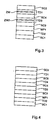
- FIG. 1 shows a stacked monolithic upright-metamorphic multiple solar cell S having a first subcell SC1 as the bottom subcell followed by a metamorphic buffer MP1, a tunnel diode TD1 and a second subcell SC2 as the top subcell.
- the first subcell SC1 has a first band gap EG1 and a first lattice constant A1 and consists of more than 50% germanium.
- the second sub-cell has a second band gap EG2 and a second lattice constant A2, the second band gap EG2 being larger than the first band gap EG1 and the second lattice constant A2 differing from the first lattice constant A1.
- the metamorphic buffer MP1 compensates for the differences between the lattice constants A1 and A2 and for this purpose comprises a sequence of at least three layers with lattice constants increasing from layer to layer in the direction of the second subcell SC2.
- the tunnel diode TD1 is arranged between the metamorphic buffer MP1 and the second subcell SC2 and has an n + layer, a p + layer and an intermediate layer ZW arranged between the n + layer and the p + layer.
- the n + layer of the first tunnel diode TD1 comprises InAlP and the p + layer of the first tunnel diode TD1 comprises an As-containing III-V material.
- the intermediate layer ZW is in each case thinner than the n + layer and as the p + layer.
- the multiple solar cell S additionally comprises a third sub-cell SC3 and a fourth sub-cell SC4, the two further sub-cells SC3 and SC4 each being designed to match the second sub-cell SC2 and arranged between the metamorphic buffer MP1 and the tunnel diode TD1.
- the multiple solar cell S also comprises a further tunnel diode TD3 with an intermediate layer according to the invention.
- the n + layer of the further tunnel diode comprises InAlP or InGaP, the p + layer of the further tunnel diode comprising an As-containing III-V material.
- a second tunnel diode TD2 between the metamorphic buffer MP1 and the first subcell SC1 comprises an n + layer and a p + layer, but no intermediate layer
- the third tunnel diode TD3 is between the third sub-cell SC3 and the fourth sub-cell SC4 in accordance with the first tunnel diode TD1.
- the third tunnel diode TD3 accordingly has a further intermediate layer ZW2 between a p + layer and an n + layer.
- the first sub-cell SC1 is designed as a Ge solar cell or substrate, the third sub-cell SC3 comprises InGaAs, the fourth sub-cell SC4 InAlGaAs and the second sub-cell InAlGaP.
- the p + layer of the first tunnel diode TD1 comprises AlInGaAs, the n + layer comprises InAlP and the intermediate layer ZW comprises Ga (Al) As.
- the multiple solar cell is designed as a 5-fold cell.
- a second tunnel diode TD2 is arranged on the first sub-cell SC1, which is designed as a Ge substrate, the second tunnel diode TD2 not comprising an intermediate layer.
- the second tunnel diode TD2 is followed by the metamorphic buffer MP1, a third partial cell SC3 made of InGaAs, a third tunnel diode TD3, a fourth partial cell made of InAlGaAs, a fourth tunnel diode TD4, a fifth partial cell made of InGaP, the first tunnel diode TD1 and the second partial cell made of InAlGaP .
- the first tunnel diode comprises an AlInGaAs layer as a p + layer, an InAlP layer as an n + layer and between the n + layer and the p + layer an intermediate layer ZW made of Ga (Al) As.
- the second tunnel diode TD2 has no intermediate layer.
- the third and fourth tunnel diodes TD3 and TD4 have no intermediate layer on.
- the n + layer of the third and fourth tunnel diodes comprises InGaP or InAlP.
- the fourth tunnel diode TD4 also comprises an intermediate layer.
- the third tunnel diode TD3 also comprises an intermediate layer.
Landscapes
- Engineering & Computer Science (AREA)
- Life Sciences & Earth Sciences (AREA)
- Computer Hardware Design (AREA)
- Microelectronics & Electronic Packaging (AREA)
- Physics & Mathematics (AREA)
- Condensed Matter Physics & Semiconductors (AREA)
- Electromagnetism (AREA)
- General Physics & Mathematics (AREA)
- Power Engineering (AREA)
- Sustainable Energy (AREA)
- Sustainable Development (AREA)
- Chemical & Material Sciences (AREA)
- Crystallography & Structural Chemistry (AREA)
- Inorganic Chemistry (AREA)
- Manufacturing & Machinery (AREA)
- Photovoltaic Devices (AREA)
Abstract
Description
- Die Erfindung betrifft eine stapelförmige, monolithische, aufrecht-metamorphe Mehrfachsolarzelle.
- Ein monolithischer aufrecht-metamorpher Solarzellenstapel ist aus W. Guter et al, "Investigation and development of III-V-triple-junction concentrator solar cells", in 22nd European Photovoltaic Solar Energy Conference, 3-7 September 2007, Milan Italy, S.122-125, bekannt.
- Aus der
EP 2 251 912 A1 ist eine stapelförmige monolithische Mehrfachsolarzelle mit verbesserter Stromleitung zwischen den Solarzellen bekannt. Hierzu wird zwischen zwei aufeinanderfolgenden Solarzellen eine Tunneldiode mit zueinander verspannten entarteten Schichten angeordnet. - Eine tensil verspannte entartete Schicht ist mit einer kompressiv verspannten entarteten Schicht kompensiert. Die entarteten Schichten sind entweder als mit Kohlenstoff dotierte entartete p+- oder als mit Tellur oder Silizium dotierte entartete n+-Schichten ausgeführt. Indem die Verspannung kompensiert ist, wirkt keine Verspannung auf die die Tunneldiode umgebenden Schichten, anders ausgedrückt die Summe der Verspannung ist null.
- Aus der
US 2010/0319764 A1 ist eine Mehrfachsolarzelle mit einer Nitridhaltigen Teilzelle bekannt, wobei eine Steigerung des Tunnelstroms der Mehrfachsolarzelle durch eine Wärmebehandlung erreicht wird. Negative Einflüsse der Wärmebehandlung werden auf die Tunneldioden werden verhindert, indem die Tunneldioden eine Schichtfolge aus mehreren n- und p-dotierten Schichten und eine ErAs-Zwischenschicht umfassen. - In "Numerical analysis of p-GaAs/n-GaAs tunnel junction emplying InAs intermediate layer for high concentrated photovoltaic applications", Seokjin Kang et al., Journal of Physics: conference Series, 490, 2014, 012178. ISSN 1742-6596 werden Untersuchungsergebnisse zu einer Zweifachsolarzelle mit GaAs-Tunneldiode mit dünner InAs-Zwischenschicht vorgestellt.
- Verschiedene Mehrfachsolarzellen sind aus der
US 2017/0222066 A1 sowie aus derEP 1 134 813 A2 bekannt. - Vor diesem Hintergrund besteht die Aufgabe der Erfindung darin, eine Vorrichtung anzugeben, die den Stand der Technik weiterbildet.
- Die Aufgabe wird durch eine Mehrfachsolarzelle mit den Merkmalen des Patentanspruchs 1 gelöst. Vorteilhafte Ausgestaltungen der Erfindung sind Gegenstand von Unteransprüchen.
- Gemäß dem Gegenstand der Erfindung wird eine stapelförmige monolithische aufrecht-metamorphe Mehrfachsolarzelle bereitgestellt, aufweisend mindestens eine erste Teilzelle, eine zweite Teilzelle, einen metamorphen Puffer und mindestens eine erste Tunneldiode.
- Die erste Teilzelle weist eine erste Bandlücke und eine erste Gitterkonstante auf und besteht zu mehr als 50% aus Germanium.
- Die zweite Teilzelle ist über der ersten Teilzelle angeordnet und weist eine zweite Bandlücke und eine zweite Gitterkonstante auf, wobei die zweite Bandlücke größer als die erste Bandlücke und die zweite Gitterkonstante größer als die erste Gitterkonstante ist.
- Der metamorphe Puffer ist zwischen der ersten Teilzelle und der zweiten Teilzelle angeordnet.
- Die erste Tunneldiode ist zwischen dem metamorphen Puffer und der zweiten Teilzelle angeordnet und weist eine n+-Schicht und eine p+-Schicht auf. Die n+-Schicht der ersten Tunneldiode umfasst InAlP, die p+-Schicht der ersten Tunneldiode umfasst ein As-haltiges III-V Material. Zwischen der n+-Schicht und der p+-Schicht ist eine Zwischenschicht angeordnet, wobei die Zwischenschicht jeweils dünner ist als die n+-Schicht und als die p+-Schicht.
- Es versteht sich weiterhin, dass der Begriff der Teilzelle synonym mit dem Begriff der Teilsolarzelle verwendet wird. Anders ausgedrückt besteht der Solarzellenstapel aus mehreren Teilsolarzellen, die miteinander mittels Tunneldioden in Serie verschaltet sind.
- Es sei angemerkt, dass die verschiedenen Schichten neben den angegebenen Materialien, beispielsweise InAlP oder As-haltiges III-V Material, zusätzlich auch weitere Elemente umfassen können.
- Auch sei angemerkt, dass die Zwischenschicht einteilig ausgebildet ist und epitaktisch mittels MOVPE hergestellt wird. Es versteht sich, dass zwischen zwei Teilzellen jeweils eine Tunneldiode ausgebildet ist.
- Des Weiteren sei angemerkt, dass der metamorphe Puffer vorzugsweise eine Abfolge von mindestens drei Schichten umfasst, wobei jede Schicht eine Gitterkonstante aufweist und die Gitterkonstanten der Schichten in Richtung der zweiten Teilzelle von Schicht zu Schicht ansteigt.
- Alternativ weist der metamorphe Puffer zwischen einer unteren Schicht und einer oberen Schicht eine nahezu lineare Änderung der Gitterkonstanten und / oder der Dotierung auf.
- Bestehen Schichten aus einer gegebenen Materialkomposition, versteht es sich, dass zusätzlich zu der angeführten Materialkomposition insbesondere Dotierstoffe wie beispielsweise Zink oder Kohlenstoff oder Silizium mitumfasst sind, ohne dass die Dotierstoffe explizit erwähnt sind.
- Ein Vorteil der erfindungsgemäßen Zwischenschicht ist, dass mittels der Zwischenschicht ein unerwünschter Einbau von einem n-Dotierstoff in die p+-Schicht der Tunneldiode verringern lässt. Anders ausgedrückt, es lässt sich eine Cross-Kontamination verringern.
- Es zeigte sich in überraschender Weise, dass sich der unerwünschte Einbau des n-Dotierstoffs mittels As-haltigen Schichten besser unterdrücken lässt, als mit phosphidhaltigen Schichten. Der Fachmann ist bisher fälschlicherweise davon ausgegangen, dass sich As-haltige Schichten, insbesondere GaAs wegen den Absorptionsverlusten nicht eignen. Durch die Absorptionsverluste wird der Wirkungsgrad der Mehrfachzelle verringert, indem die darunter liegenden Teilzellen weniger Licht erhalten.
- Die störende Absorption lässt sich jedoch unterdrücken, indem die GaAs Schicht sehr dünn, d.h. wenige nm dick auszuführen ist, dass sich in den Quantentöpfen der As-haltigen Zwischenschicht keine Zustände bzw. keine absorbierende Niveaus befinden.
- Hierdurch ist es möglich eine hohe Transparenz der Tunneldiode für die unter der Tunneldiode liegenden Teilzellen zu erreichen und gleichzeitig eine Tunneldiode mit einer hohen Peakstromdichte bereitzustellen und den Wirkungsgrad der Mehrfachsolarzelle zu erhöhen.
- Gemäß einer ersten Ausführungsform umfasst die n+-Schicht der ersten Tunneldiode InxAlx-1P mit x > 0,55 oder mit x > 0,6 oder mit x ≥ 0,65. InAlP bildet mit diesem ausreichend hohen Indium-Gehalt einen direkten Halbleiter. Im Vergleich zu üblichen InGaAs-oder InGaP Schichten wird eine deutlich höhere Transparenz erreicht.
- Einer aufgrund der höheren Bandlücke von InAlP auftretenden Reduktion des Tunnelstroms wird durch die erfindungsgemäße Zwischenschicht, bevorzugt eine GaAs-Zwischenschicht, entgegengewirkt.
- Auch zeigt sich, dass InAlP mit einem niedrigeren Inidum-Gehalt, z.B. x < 0,5 für die n+-Schicht überraschenderweise nicht geeignet ist, da es einen indirekten Halbleiter bildet.
- In einer anderen Ausführungsform umfasst die Zwischenschicht As, wobei ein As-Gehalt der Zwischenschicht höher als ein As-Gehalt der n+-Schicht ist. Gemäß alternativer Weiterbildungen umfasst die Zwischenschicht GaAs oder AlGaAs oder AlInAs.
- Bevorzugt weist die Zwischenschicht eine Dicke kleiner 6 nm oder kleiner 4 nm auf und ist gemäß einer weiteren Ausführungsform mit Silizium mit einer Dotierstoffkonzentration von mindestens 1018 N/cm3 dotiert.
- In einer Weiterbildung weist die Zwischenschicht eine Energiebandlücke von ≥ 1.08 eV auf.
- Gemäß einer weiteren Weiterbildung ist die n+-Schicht der ersten Tunneldiode mit Silizium und/oder mit Tellur und/oder mit Selen und/oder mit Schwefel mit einer Dotierstoffkonzentration von ≥ 1019 N/cm3 dotiert.
- Die n+-Schicht der ersten Tunneldiode umfasst in einer weiteren Ausführungsform Gallium und gemäß einer Weiterbildung AlxGayIn1-x-yP mit 0 ≤ y < 0,15 oder 0 ≤ y < 0,05 oder 0 ≤ y < 0,01.
- In einer weiteren Ausführungsform umfasst die p+-Schicht der ersten Tunneldiode AlInAs und gemäß einer Weiterbildung AlxGayIn1-x-yAs mit x>0,4.
- In einer anderen Weiterbildung ist die p+-Schicht der ersten Tunneldiode mit Kohlenstoff dotiert.
- Gemäß einer anderen Ausführungsform entspricht eine Gitterkonstante der n+-Schicht der ersten Tunneldiode der zweiten Gitterkonstanten der zweiten Teilzelle und eine Gitterkonstante der p+-Schicht der ersten Tunneldiode ist gleich oder kleiner als die zweite Gitterkonstante der zweiten Teilzelle.
- In wieder einer anderen Ausführungsform weist die Mehrfachsolarzelle weitere Teilzellen auf, wobei jede Teilzelle jeweils eine weitere Bandlücke aufweist, die weiteren Teilzellen zwischen der ersten Tunneldiode und der ersten Teilzelle angeordnet sind und die Bandlücken der weiteren Teilzellen jeweils größer als die erste Bandlücke der ersten Teilzelle und jeweils kleiner als die zweite Bandlücke der zweiten Teilzelle sind.
- In einer Weiterbildung weist die Mehrfachsolarzelle mindestens eine weitere Tunneldiode auf. Die mindestens eine weitere Tunneldiode weist gemäß einer weiteren Weiterbildung eine weitere Zwischenschicht auf, wobei eine n+-Schicht der weiteren Tunneldiode InAlP oder InGaP umfasst, eine p+-Schicht der weiteren Tunneldiode ein As-haltiges III-V Material umfasst, die weitere Zwischenschicht zwischen n+-Schicht und p+-Schicht der weiteren Tunneldiode angeordnet ist und die weitere Zwischenschicht jeweils dünner als die n+-Schicht und als die p+-Schicht der weiteren Tunneldiode ist.
- Bevorzugt umfasst die unterste Tunneldiode der weiteren Tunneldioden eine andere Zusammensetzung oder ist ohne Zwischenschicht ausgebildet.
- Gemäß einer anderen Ausführungsform ist die Mehrfachzelle als Ge / InGaAs / AlInGaAs / AlInGaP 4-fach Zelle ausgebildet, wobei die n+-Schicht der ersten Tunneldiode (TD1) InAlP umfasst. Es versteht sich, dass in der Ge / InGaAs / AlInGaAs / AlInGaP 4-fach Zelle die Teilsolarzelle SC2 aus AlInGaP gebildet ist und die Tunneldiode TD1 unterhalb der AlInGaP Teilsolarzelle angeordnet ist.
- In einer anderen alternativen Ausführungsform ist die Mehrfachsolarzelle als Ge / InGaAs / AlInGaAs / InGaP/ AlInGaP 5-fach Zelle ausgebildet, wobei die n+-Schicht der ersten Tunneldiode (TD1) InAlP umfasst. Es versteht sich, dass in der Ge / InGaAs / AlInGaAs / InGaP/ AlInGaP 5-fach Zelle die Teilsolarzelle SC2 aus AlInGaP gebildet ist und die Tunneldiode TD1 unterhalb der AlInGaP Teilsolarzelle angeordnet ist.
- Die Erfindung wird nachfolgend unter Bezugnahme auf die Zeichnungen näher erläutert. Hierbei werden gleichartige Teile mit identischen Bezeichnungen beschriftet. Die dargestellten Ausführungsformen sind stark schematisiert, d.h. die Abstände und die lateralen und die vertikalen Erstreckungen sind nicht maßstäblich und weisen, sofern nicht anders angegeben, auch keine ableitbaren geometrischen Relationen zueinander auf. Darin zeigen, die:
- Figur 1
- eine schematische Ansicht auf eine erste erfindungsgemäße Ausführungsform einer stapelförmigen monolithischen aufrecht-metamorphen Mehrfachsolarzelle,
- Figur 2
- eine schematische Ansicht auf eine zweite erfindungsgemäße Ausführungsform der Mehrfachsolarzelle,
- Figur 3
- eine schematische Ansicht auf eine dritte erfindungsgemäße Ausführungsform der Mehrfachsolarzelle
- Figur 4
- eine schematische Ansicht auf eine vierte erfindungsgemäße Ausführungsform der Mehrfachsolarzelle.
- Die Abbildung der
Figur 1 zeigt eine stapelförmige monolithische aufrecht-metamorphe Mehrfachsolarzelle S aufweisend eine erste Teilzelle SC1 als unterste Teilzelle gefolgt von einem metamorphen Puffer MP1, einer Tunneldiode TD1 und einer zweite Teilzelle SC2 als oberster Teilzelle. - Die erste Teilzelle SC1 weist eine erste Bandlücke EG1 und eine erste Gitterkonstante A1 auf und besteht zu mehr als 50% aus Germanium.
- Die zweite Teilzelle weist eine zweite Bandlücke EG2 auf und eine zweite Gitterkonstante A2 auf, wobei die zweite Bandlücke EG2 größer als die erste Bandlücke EG1 ist und sich die zweite Gitterkonstante A2 von der ersten Gitterkonstante A1 unterscheidet.
- Der metamorphe Puffer MP1 gleicht die Unterschiede zwischen den Gitterkonstanten A1 und A2 aus und umfasst hierfür eine Abfolge von mindestens drei Schichten mit in Richtung der zweiten Teilzelle SC2 von Schicht zu Schicht ansteigenden Gitterkonstanten.
- Die Tunneldiode TD1 ist zwischen dem metamorphen Puffer MP1 und der zweiten Teilzelle SC2 angeordnet und weist eine n+-Schicht, eine p+-Schicht und eine zwischen der n+-Schicht und der p+-Schicht angeordnete Zwischenschicht ZW auf.
- Die n+-Schicht der ersten Tunneldiode TD1 umfasst InAlP und die p+-Schicht der ersten Tunneldiode TD1 umfasst ein As-haltiges III-V Material.
- Die Zwischenschicht ZW ist jeweils dünner ist als die n+-Schicht und als die p+-Schicht ausgebildet.
- In der Abbildung der
Figur 2 ist eine weitere Ausführungsform dargestellt. Im Folgenden werden nur die Unterschiede zu der Abbildung derFigur 1 erläutert. - Die Mehrfachsolarzelle S umfasst zusätzlich eine dritte Teilzelle SC3 und eine vierte Teilzelle SC4, wobei die beiden weiteren Teilzellen SC3 und SC4 jeweils gitterangepasst zu der zweiten Teilzelle SC2 ausgebildet und zwischen dem metamorphen Puffer MP1 und der Tunneldiode TD1 angeordnet sind.
- In der Abbildung der
Figur 3 ist eine weitere Ausführungsform dargestellt. Im Folgenden werden nur die Unterschiede zu der Abbildung derFigur 2 erläutert. - In dieser Ausführungsform umfasst die Mehrfachsolarzelle S zusätzlich zu der dritten und vierten Teilzelle SC3 und SC4 noch eine weitere Tunneldiode TD3 mit einer erfindungsgemäßen Zwischenschicht. Die n+-Schicht der weiteren Tunneldiode umfasst InAlP oder InGaP, wobei die p+-Schicht der weiteren Tunneldiode ein As-haltiges III-V Material umfasst.
- Während eine zweite Tunneldiode TD2 zwischen dem metamorphen Puffer MP1 und der ersten Teilzelle SC1 eine n+-Schicht und eine p+-Schicht, aber keine Zwischenschicht umfasst, ist die dritte Tunneldiode TD3 zwischen der dritten Teilzelle SC3 und der vierten Teilzelle SC4 entsprechend der ersten Tunneldiode TD1 aufgebaut.
- Die dritte Tunneldiode TD3 weist entsprechend zwischen einer p+-Schicht und einer n+-Schicht eine weitere Zwischenschicht ZW2 auf.
- Die erste Teilzelle SC1 ist als Ge-Solarzelle bzw. Substrat ausgebildet, die dritte Teilzelle SC3 umfasst InGaAs, die vierte Teilzelle SC4 InAlGaAs und die zweite Teilzelle InAlGaP. Die p+-Schicht der ersten Tunneldiode TD1 umfasst AlInGaAs, die n+-Schicht umfasst InAlP und die Zwischenschicht ZW umfasst Ga(Al)As.
- In der Abbildung der
Figur 4 ist eine weitere Ausführungsform dargestellt. Im Folgenden werden nur die Unterschiede zu der Abbildung derFigur 3 erläutert. - Die Mehrfachsolarzelle ist als 5-fach Zelle ausgebildet. Auf der als Ge-Substrat ausgebildeten ersten Teilzelle SC1 ist eine zweite Tunneldiode TD2 angeordnet, wobei die zweite Tunneldiode TD2 keine Zwischenschicht umfasst.
- Auf der zweiten Tunneldiode TD2 folgt der metamorphe Puffer MP1, eine dritte Teilzelle SC3 aus InGaAs, eine dritte Tunneldiode TD3, eine vierte Teilzelle aus InAlGaAs, eine vierte Tunneldiode TD4, eine fünfte Teilzelle aus InGaP, die erste Tunneldiode TD1 sowie die zweite Teilzelle aus InAlGaP.
- Die erste Tunneldiode umfasst eine AlInGaAs-Schicht als p+-Schicht, eine InAlP-Schicht als n+-Schicht und zwischen der n+-Schicht und der p+-Schicht eine Zwischenschicht ZW aus Ga(Al)As.
- Die zweite Tunneldiode TD2 weist keine Zwischenschicht auf.
- Die dritte und die vierte Tunneldiode TD3 und TD4 weisen im dargestellten Ausführungsbeispiel, wie die zweite Tunneldiode TD1, keine Zwischenschicht auf. Im dargestellten Ausführungsbeispiel umfasst die n+-Schicht der dritten und vierten Tunneldiode InGaP oder InAlP.
- Alternativ umfasst auch die vierte Tunneldiode TD4 eine Zwischenschicht. Wiederum alternativ umfasst zusätzlich zu der vierten Tunneldiode TD4 auch die dritte Tunneldiode TD3 eine Zwischenschicht.
Claims (15)
- Stapelförmige monolithische aufrecht-metamorphe Mehrfachsolarzelle (S) aufweisend- mindestens eine erste Teilzelle (SC1) mit einer ersten Bandlücke (EG1), einer ersten Gitterkonstante (A1) und zu mehr als 50% aus Germanium bestehend,- eine über der ersten Teilzelle (SC1) angeordnete zweite Teilzelle (SC2) mit einer zweiten Bandlücke (EG2) und einer zweiten Gitterkonstante (A2),- einen zwischen der ersten Teilzelle (SC1) und der zweiten Teilzelle (SC2) angeordneten metamorphen Puffer (MP1), und- eine zwischen dem metamorphen Puffer (MP1) und der zweiten Teilzelle (SC2) angeordnete erste Tunneldiode (TD1) mit einer n+-Schicht und einer p+-Schicht, wobei- die p+-Schicht der ersten Tunneldiode (TD1) ein As-haltiges III-V Material umfasst,- die zweite Bandlücke (EG2) größer als die erste Bandlücke (EG1) ist und- die zweite Gitterkonstante (A2) größer als die erste Gitterkonstante (A1) ist,dadurch gekennzeichnet, dass- die n+-Schicht der ersten Tunneldiode (TD1) InxAlx-1P mit x > 0,55 oder mit x > 0,6 oder mit x ≥ 0,65 umfasst,-- zwischen der n+-Schicht und der p+-Schicht eine Zwischenschicht (ZW) angeordnet ist,- die Zwischenschicht (ZW) jeweils dünner ist als die n+-Schicht und als die p+-Schicht,- die Zwischenschicht (ZW) eine Dicke (Dzw) kleiner 6 nm oder kleiner 4 nm aufweist und- die Zwischenschicht GaAs oder AlGaAs oder AlInAs oder InGaAs oder AlInGaAs umfasst.
- Mehrfachsolarzelle nach Anspruch 1, dadurch gekennzeichnet, dass die Zwischenschicht (ZW) As umfasst, wobei ein As-Gehalt der Zwischenschicht (ZW) höher als ein As-Gehalt der n+-Schicht ist.
- Mehrfachsolarzelle nach einem der vorangegangenen Ansprüche, dadurch gekennzeichnet, dass die Zwischenschicht (ZW) eine Energiebandlücke von ≥ 1.08 eV aufweist.
- Mehrfachsolarzelle nach einem der vorangegangenen Ansprüche, dadurch gekennzeichnet, dass die Zwischenschicht (ZW) mit Silizium mit einer Dotierstoffkonzentration von mindestens 1018 N/cm3 dotiert ist.
- Mehrfachsolarzelle nach einem der vorangegangenen Ansprüche, dadurch gekennzeichnet, dass die n+-Schicht der ersten Tunneldiode (TD1) mit Silizium und/oder mit Tellur und/oder mit Selen und/oder mit Schwefel mit einer Dotierstoffkonzentration von ≥1019 N/cm3 dotiert ist.
- Mehrfachsolarzelle nach einem der vorangegangenen Ansprüche, dadurch gekennzeichnet, dass die n+-Schicht der ersten Tunneldiode (TD1) Gallium umfasst.
- Mehrfachsolarzelle nach einem der vorangegangenen Ansprüche, dadurch gekennzeichnet, dass die n+-Schicht der ersten Tunneldiode (TD1) AlxGayIn1-x-yP mit 0 ≤ y < 0,15 oder 0 ≤ y < 0,05 oder 0 ≤ y < 0,01 umfasst.
- Mehrfachsolarzelle nach einem der vorangegangenen Ansprüche, dadurch gekennzeichnet, dass die p+-Schicht der ersten Tunneldiode (TD1) AlInAs umfasst.
- Mehrfachsolarzelle nach einem der vorangegangenen Ansprüche, dadurch gekennzeichnet, dass die p+-Schicht der ersten Tunneldiode (TD1) AlxGayIn1-x-yAs mit x>0,4 umfasst.
- Mehrfachsolarzelle nach einem der vorangegangenen Ansprüche, dadurch gekennzeichnet, dass die p+-Schicht der ersten Tunneldiode (TD1) mit Kohlenstoff dotiert ist.
- Mehrfachsolarzelle nach einem der vorangegangenen Ansprüche, dadurch gekennzeichnet, dass eine Gitterkonstante der n+-Schicht der ersten Tunneldiode (TD1) der zweiten Gitterkonstanten (A2) der zweiten Teilzelle (SC2) entspricht und eine Gitterkonstante der p+-Schicht der ersten Tunneldiode (TD1) gleich oder kleiner als die zweite Gitterkonstante (A2) der zweiten Teilzelle (SC2) ist.
- Mehrfachsolarzelle nach einem der vorangegangenen Ansprüche, dadurch gekennzeichnet, dass die Mehrfachsolarzelle weitere Teilzellen (SC3, SC4) jeweils mit weiterer Bandlücke (EG3, EG4) aufweist, wobei die weiteren Teilzellen (SC3, SC4) zwischen der ersten Tunneldiode (TD1) und der ersten Teilzelle (SC1) angeordnet sind und die Bandlücken (EG3, EG4) der weiteren Teilzellen (SC3, SC4) jeweils größer als die erste Bandlücke (EG1) der ersten Teilzelle (SC1) und jeweils kleiner als die zweite Bandlücke (EG2) der zweiten Teilzelle (SC2) sind.
- Mehrfachsolarzelle nach Anspruch 12, dadurch gekennzeichnet, dass die Mehrfachsolarzelle mindestens eine weitere Tunneldiode (TD2, TD3) aufweist.
- Mehrfachsolarzelle nach Anspruch 12 oder 13, dass die mindestens eine weitere Tunneldiode (TD3) eine weitere Zwischenschicht (ZW2) aufweist, wobei eine n+-Schicht der weiteren Tunneldiode (TD3) InAlP oder InGaP umfasst, eine p+-Schicht der weiteren Tunneldiode (TD3) ein As-haltiges III-V Material umfasst, die weitere Zwischenschicht (ZW2) zwischen n+-Schicht und p+-Schicht der weiteren Tunneldiode (TD3) angeordnet ist und die weitere Zwischenschicht (ZW2) jeweils dünner ist als die n+-Schicht und als die p+-Schicht der weiteren Tunneldiode (TD3) ist.
- Mehrfachsolarzelle nach einem der Ansprüche 12 bis 14, dadurch gekennzeichnet, dass die Mehrfachsolarzelle als Ge / InGaAs / AlInGaAs / AlInGaP 4-fach Zelle ausgebildet ist oder die Mehrfachsolarzelle als Ge / InGaAs / AlInGaAs / InGaP/ AlInGaP 5-fach Zelle ausgebildet ist.
Applications Claiming Priority (1)
| Application Number | Priority Date | Filing Date | Title |
|---|---|---|---|
| DE102018009744.8A DE102018009744A1 (de) | 2018-12-14 | 2018-12-14 | Stapelförmige monolithische aufrecht-metamorphe Mehrfachsolarzelle |
Publications (1)
| Publication Number | Publication Date |
|---|---|
| EP3667742A1 true EP3667742A1 (de) | 2020-06-17 |
Family
ID=68766451
Family Applications (1)
| Application Number | Title | Priority Date | Filing Date |
|---|---|---|---|
| EP19000542.1A Pending EP3667742A1 (de) | 2018-12-14 | 2019-12-02 | Stapelförmige monolithische aufrecht-metamorphe mehrfachsolarzelle |
Country Status (4)
| Country | Link |
|---|---|
| US (1) | US20200194607A1 (de) |
| EP (1) | EP3667742A1 (de) |
| CN (1) | CN111326597B (de) |
| DE (1) | DE102018009744A1 (de) |
Cited By (1)
| Publication number | Priority date | Publication date | Assignee | Title |
|---|---|---|---|---|
| EP3872869A1 (de) * | 2020-02-25 | 2021-09-01 | AZUR SPACE Solar Power GmbH | Stapelförmige monolithische aufrecht-metamorphe iii-v-mehrfachsolarzelle |
Families Citing this family (2)
| Publication number | Priority date | Publication date | Assignee | Title |
|---|---|---|---|---|
| EP3937259A1 (de) * | 2020-07-10 | 2022-01-12 | AZUR SPACE Solar Power GmbH | Monolithische metamorphe mehrfachsolarzelle |
| EP3965169B1 (de) * | 2020-09-07 | 2023-02-15 | AZUR SPACE Solar Power GmbH | Stapelförmige monolithische mehrfachsolarzelle |
Citations (7)
| Publication number | Priority date | Publication date | Assignee | Title |
|---|---|---|---|---|
| EP1134813A2 (de) | 2000-03-15 | 2001-09-19 | The Boeing Company | Photovoltaische Zelle mit mehreren Übergängen mit dünner erster (oberer) Unterzelle und dickerer zweiter Unterzelle aus dem gleichen oder ähnlichem Halbleitermaterial |
| EP2251912A1 (de) | 2009-05-11 | 2010-11-17 | Fraunhofer-Gesellschaft zur Förderung der angewandten Forschung e.V. | Tunneldioden aus spannungskompensierten Verbindungshalbleiterschichten |
| US20100319764A1 (en) | 2009-06-23 | 2010-12-23 | Solar Junction Corp. | Functional Integration Of Dilute Nitrides Into High Efficiency III-V Solar Cells |
| JP2011077293A (ja) * | 2009-09-30 | 2011-04-14 | Asahi Kasei Electronics Co Ltd | 多接合型太陽電池 |
| US20170077340A1 (en) * | 2014-07-11 | 2017-03-16 | Rich Company, Ltd. | Compound-semiconductor photovoltaic cell and manufacturing method of compound-semiconductor photovoltaic cell |
| US20170222066A1 (en) | 2016-01-28 | 2017-08-03 | Solaero Technologies Corp. | Multijunction metamorphic solar cell for space applications |
| US20180315879A1 (en) * | 2017-04-27 | 2018-11-01 | Alliance For Sustainable Energy, Llc | Tunnel junctions for multijunction solar cells |
Family Cites Families (8)
| Publication number | Priority date | Publication date | Assignee | Title |
|---|---|---|---|---|
| US5407491A (en) * | 1993-04-08 | 1995-04-18 | University Of Houston | Tandem solar cell with improved tunnel junction |
| US5753050A (en) * | 1996-08-29 | 1998-05-19 | The United States Of America As Represented By The Department Of Energy | Thermophotovoltaic energy conversion device |
| US8067687B2 (en) * | 2002-05-21 | 2011-11-29 | Alliance For Sustainable Energy, Llc | High-efficiency, monolithic, multi-bandgap, tandem photovoltaic energy converters |
| US8299351B2 (en) * | 2009-02-24 | 2012-10-30 | Hong Kong Applied Science And Technology Research Institute Co., Ltd. | Epitaxial growth of III-V compounds on (111) silicon for solar cells |
| DE102012004734A1 (de) * | 2012-03-08 | 2013-09-12 | Fraunhofer-Gesellschaft zur Förderung der angewandten Forschung e.V. | Mehrfachsolarzelle und deren Verwendung |
| EP2650930A1 (de) * | 2012-04-12 | 2013-10-16 | AZURSPACE Solar Power GmbH | Solarzellenstapel |
| US20180240922A1 (en) * | 2015-08-17 | 2018-08-23 | Solaero Technologies Corp. | Four junction solar cell and solar cell assemblies for space applications |
| DE102015016822B4 (de) * | 2015-12-25 | 2023-01-05 | Azur Space Solar Power Gmbh | Stapelförmige Mehrfach-Solarzelle |
-
2018
- 2018-12-14 DE DE102018009744.8A patent/DE102018009744A1/de active Pending
-
2019
- 2019-12-02 EP EP19000542.1A patent/EP3667742A1/de active Pending
- 2019-12-13 CN CN201911281644.1A patent/CN111326597B/zh active Active
- 2019-12-16 US US16/715,388 patent/US20200194607A1/en active Pending
Patent Citations (7)
| Publication number | Priority date | Publication date | Assignee | Title |
|---|---|---|---|---|
| EP1134813A2 (de) | 2000-03-15 | 2001-09-19 | The Boeing Company | Photovoltaische Zelle mit mehreren Übergängen mit dünner erster (oberer) Unterzelle und dickerer zweiter Unterzelle aus dem gleichen oder ähnlichem Halbleitermaterial |
| EP2251912A1 (de) | 2009-05-11 | 2010-11-17 | Fraunhofer-Gesellschaft zur Förderung der angewandten Forschung e.V. | Tunneldioden aus spannungskompensierten Verbindungshalbleiterschichten |
| US20100319764A1 (en) | 2009-06-23 | 2010-12-23 | Solar Junction Corp. | Functional Integration Of Dilute Nitrides Into High Efficiency III-V Solar Cells |
| JP2011077293A (ja) * | 2009-09-30 | 2011-04-14 | Asahi Kasei Electronics Co Ltd | 多接合型太陽電池 |
| US20170077340A1 (en) * | 2014-07-11 | 2017-03-16 | Rich Company, Ltd. | Compound-semiconductor photovoltaic cell and manufacturing method of compound-semiconductor photovoltaic cell |
| US20170222066A1 (en) | 2016-01-28 | 2017-08-03 | Solaero Technologies Corp. | Multijunction metamorphic solar cell for space applications |
| US20180315879A1 (en) * | 2017-04-27 | 2018-11-01 | Alliance For Sustainable Energy, Llc | Tunnel junctions for multijunction solar cells |
Non-Patent Citations (4)
| Title |
|---|
| CAMPESATO R ET AL: "High efficiency solar cells based on AlInGaP", PHOTOVOLTAIC SPECIALISTS CONFERENCE (PVSC), 2009 34TH IEEE, IEEE, PISCATAWAY, NJ, USA, 7 June 2009 (2009-06-07), pages 1112 - 1117, XP031626502, ISBN: 978-1-4244-2949-3 * |
| ENRIQUE BARRIGÓN ET AL: "Highly conductive p++AlGaAs/n++GaInP tunnel junctions for ultra-high concentrator solar cells", PROGRESS IN PHOTOVOLTAICS: RESEARCH AND APPLICATIONS, vol. 22, no. 4, 15 February 2014 (2014-02-15), pages 399 - 404, XP055203912, ISSN: 1062-7995, DOI: 10.1002/pip.2476 * |
| KANG ET AL., JOURNAL OF PHYSICS: CONFERENCE SERIES, vol. 490, 2014, pages 012178, ISSN: 1742-6596 |
| W. GUTER ET AL.: "Investigation and development of III-V-tripie-junction concentrator solar cells", 22ND EUROPEAN PHOTOVOLTAIC SOLAR ENERGY CONFERENCE, 3 September 2007 (2007-09-03), pages 122 - 125 |
Cited By (1)
| Publication number | Priority date | Publication date | Assignee | Title |
|---|---|---|---|---|
| EP3872869A1 (de) * | 2020-02-25 | 2021-09-01 | AZUR SPACE Solar Power GmbH | Stapelförmige monolithische aufrecht-metamorphe iii-v-mehrfachsolarzelle |
Also Published As
| Publication number | Publication date |
|---|---|
| DE102018009744A1 (de) | 2020-06-18 |
| CN111326597A (zh) | 2020-06-23 |
| US20200194607A1 (en) | 2020-06-18 |
| CN111326597B (zh) | 2023-07-04 |
Similar Documents
| Publication | Publication Date | Title |
|---|---|---|
| EP3419060B1 (de) | Solarzellenstapel | |
| EP2430672B1 (de) | Tunneldioden aus spannungskompensierten verbindungshalbleiterschichten | |
| EP3179521A1 (de) | Mehrfach-solarzelle | |
| EP3667742A1 (de) | Stapelförmige monolithische aufrecht-metamorphe mehrfachsolarzelle | |
| DE102008034711A1 (de) | Barrierenschichten in invertierten metamorphen Multijunction-Solarzellen | |
| EP3185312B1 (de) | Stapelförmige mehrfach-solarzelle | |
| EP2919276A1 (de) | Mehrfach-Solarzelle | |
| EP3012874B1 (de) | Stapelförmige integrierte Mehrfachsolarzelle | |
| EP2960950A1 (de) | Mehrfach-Solarzelle | |
| DE102016111844A1 (de) | Leistungshalbleitervorrichtung | |
| DE102015006379B4 (de) | Skalierbare Spannungsquelle | |
| DE102015012007A1 (de) | Skalierbare Spannungsquelle | |
| EP3065177B1 (de) | Solarzellenvorrichtung | |
| DE102015013514B4 (de) | Optischer Empfängerbaustein | |
| EP3712965A1 (de) | Stapelförmige, monolithische, aufrecht metamorphe, terrestrische konzentrator-solarzelle | |
| EP3937259A1 (de) | Monolithische metamorphe mehrfachsolarzelle | |
| DE102018009850A1 (de) | Stapelförmige Mehrfachsolarzelle | |
| EP3937260A1 (de) | Monolithische metamorphe mehrfachsolarzelle | |
| DE102016208113A1 (de) | Mehrfachsolarzelle und deren Verwendung | |
| EP3734667A1 (de) | Stapelförmige hochsperrende iii-v-halbleiterleistungsdiode | |
| EP3965169B1 (de) | Stapelförmige monolithische mehrfachsolarzelle | |
| DE102020001185A1 (de) | Stapelförmige monolithische aufrecht-metamorphe lll-V-Mehrfachsolarzelle | |
| DE102019003068A1 (de) | Stapelförmige hochsperrende lnGaAS-Halbleiterleistungsdiode | |
| EP3799136B1 (de) | Monolithische mehrfachsolarzelle mit genau vier teilzellen | |
| DE102020000549B4 (de) | Stapelförmiges photonisches III-V-Halbleiterbauelement |
Legal Events
| Date | Code | Title | Description |
|---|---|---|---|
| PUAI | Public reference made under article 153(3) epc to a published international application that has entered the european phase |
Free format text: ORIGINAL CODE: 0009012 |
|
| STAA | Information on the status of an ep patent application or granted ep patent |
Free format text: STATUS: THE APPLICATION HAS BEEN PUBLISHED |
|
| STAA | Information on the status of an ep patent application or granted ep patent |
Free format text: STATUS: REQUEST FOR EXAMINATION WAS MADE |
|
| AK | Designated contracting states |
Kind code of ref document: A1 Designated state(s): AL AT BE BG CH CY CZ DE DK EE ES FI FR GB GR HR HU IE IS IT LI LT LU LV MC MK MT NL NO PL PT RO RS SE SI SK SM TR |
|
| AX | Request for extension of the european patent |
Extension state: BA ME |
|
| 17P | Request for examination filed |
Effective date: 20200529 |
|
| RBV | Designated contracting states (corrected) |
Designated state(s): AL AT BE BG CH CY CZ DE DK EE ES FI FR GB GR HR HU IE IS IT LI LT LU LV MC MK MT NL NO PL PT RO RS SE SI SK SM TR |
|
| STAA | Information on the status of an ep patent application or granted ep patent |
Free format text: STATUS: EXAMINATION IS IN PROGRESS |
|
| 17Q | First examination report despatched |
Effective date: 20221021 |