EP3667535A1 - Vorrichtung und verfahren zur verschlüsselung und entschlüsselung von speicherdaten - Google Patents
Vorrichtung und verfahren zur verschlüsselung und entschlüsselung von speicherdaten Download PDFInfo
- Publication number
- EP3667535A1 EP3667535A1 EP18842975.7A EP18842975A EP3667535A1 EP 3667535 A1 EP3667535 A1 EP 3667535A1 EP 18842975 A EP18842975 A EP 18842975A EP 3667535 A1 EP3667535 A1 EP 3667535A1
- Authority
- EP
- European Patent Office
- Prior art keywords
- data
- encryption
- decryption
- memory
- keys
- Prior art date
- Legal status (The legal status is an assumption and is not a legal conclusion. Google has not performed a legal analysis and makes no representation as to the accuracy of the status listed.)
- Granted
Links
- 238000000034 method Methods 0.000 title claims abstract description 23
- 238000013500 data storage Methods 0.000 claims description 32
- 238000000638 solvent extraction Methods 0.000 claims description 4
- 230000008707 rearrangement Effects 0.000 claims description 3
- 238000010586 diagram Methods 0.000 description 4
- 238000005516 engineering process Methods 0.000 description 2
- 230000001133 acceleration Effects 0.000 description 1
- 239000000969 carrier Substances 0.000 description 1
- 238000010276 construction Methods 0.000 description 1
- 230000006870 function Effects 0.000 description 1
- 230000006872 improvement Effects 0.000 description 1
- 230000007246 mechanism Effects 0.000 description 1
- 230000004044 response Effects 0.000 description 1
Images


Classifications
-
- G—PHYSICS
- G06—COMPUTING; CALCULATING OR COUNTING
- G06F—ELECTRIC DIGITAL DATA PROCESSING
- G06F12/00—Accessing, addressing or allocating within memory systems or architectures
- G06F12/14—Protection against unauthorised use of memory or access to memory
- G06F12/1408—Protection against unauthorised use of memory or access to memory by using cryptography
-
- H—ELECTRICITY
- H04—ELECTRIC COMMUNICATION TECHNIQUE
- H04L—TRANSMISSION OF DIGITAL INFORMATION, e.g. TELEGRAPHIC COMMUNICATION
- H04L9/00—Cryptographic mechanisms or cryptographic arrangements for secret or secure communications; Network security protocols
- H04L9/08—Key distribution or management, e.g. generation, sharing or updating, of cryptographic keys or passwords
- H04L9/0894—Escrow, recovery or storing of secret information, e.g. secret key escrow or cryptographic key storage
-
- G—PHYSICS
- G06—COMPUTING; CALCULATING OR COUNTING
- G06F—ELECTRIC DIGITAL DATA PROCESSING
- G06F21/00—Security arrangements for protecting computers, components thereof, programs or data against unauthorised activity
- G06F21/60—Protecting data
- G06F21/602—Providing cryptographic facilities or services
-
- G—PHYSICS
- G06—COMPUTING; CALCULATING OR COUNTING
- G06F—ELECTRIC DIGITAL DATA PROCESSING
- G06F21/00—Security arrangements for protecting computers, components thereof, programs or data against unauthorised activity
- G06F21/70—Protecting specific internal or peripheral components, in which the protection of a component leads to protection of the entire computer
- G06F21/78—Protecting specific internal or peripheral components, in which the protection of a component leads to protection of the entire computer to assure secure storage of data
- G06F21/79—Protecting specific internal or peripheral components, in which the protection of a component leads to protection of the entire computer to assure secure storage of data in semiconductor storage media, e.g. directly-addressable memories
-
- G—PHYSICS
- G06—COMPUTING; CALCULATING OR COUNTING
- G06F—ELECTRIC DIGITAL DATA PROCESSING
- G06F7/00—Methods or arrangements for processing data by operating upon the order or content of the data handled
- G06F7/58—Random or pseudo-random number generators
- G06F7/588—Random number generators, i.e. based on natural stochastic processes
-
- H—ELECTRICITY
- H04—ELECTRIC COMMUNICATION TECHNIQUE
- H04L—TRANSMISSION OF DIGITAL INFORMATION, e.g. TELEGRAPHIC COMMUNICATION
- H04L9/00—Cryptographic mechanisms or cryptographic arrangements for secret or secure communications; Network security protocols
- H04L9/14—Cryptographic mechanisms or cryptographic arrangements for secret or secure communications; Network security protocols using a plurality of keys or algorithms
Definitions
- the present invention relates to the field of computer device science and technologies, and in particular, to a storage data encryption and decryption apparatus and method.
- SoC System on Chip
- a storage data encryption and decryption apparatus and method provided in the present invention can encrypt and decrypt data in different chips or different storage areas of the same chip by using different keys, so as to overcome the shortcomings in the prior art, thus implementing data storage, reading and writing operations efficiently.
- the present invention provides a storage data encryption and decryption method, including:
- the foregoing step 3 further includes judging whether to separate data in the data memory:
- keys of respective data storage areas used for selectively performing encryption and decryption operations on the data of the plurality of data storage areas are different from each other; and a unified key is used for performing encryption and decryption operations on the data of the entire data storage area.
- keys used for performing encryption and decryption operations on the same data storage area in the plurality of data storage areas of different chips are different from each other; and keys used for performing encryption and decryption operations on the data of the entire data storage area of different chips are different from each other.
- encryption and decryption algorithms used by the data encryption and decryption module are completed in a single cycle.
- the encryption and decryption algorithms used by the data encryption and decryption module include exclusive OR and sequence rearrangement.
- the data encryption and decryption module automatically acquires the keys in the key memory by hardware when a system chip is started.
- the data memory and the key memory are located on the same physical medium.
- the method further includes that the keys stored in the key memory can be cleared when the system is attacked.
- the present invention provides a storage data encryption and decryption apparatus that uses the foregoing method, including:
- the storage data encryption and decryption apparatus and method provided in embodiments of the present invention can implement encryption of data in different chips or different storage areas of the same chip in a clock cycle, thus implementing data storage, reading and writing operations securely and efficiently.
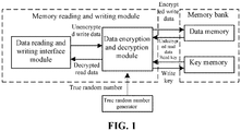
- FIG. 1 is a schematic structural diagram of a storage data encryption and decryption apparatus according to an embodiment of the present invention.
- the storage data encryption and decryption apparatus includes a memory module, a memory bank, and a true random number generator.
- the memory module is configured to support data and key reading and writing and perform encryption and decryption operations on data passing through the module.
- the memory bank is configured to support a data and key storage function.
- the true random number generator is configured to generate keys.
- a memory reading and writing module is responsible for encrypting write data and writing the encrypted write data into the memory bank, and decrypting read data that is read from the memory bank.
- the memory reading and writing module consists of a data reading and writing interface module and a data encryption and decryption module.
- the data reading and writing interface module is configured to read and write data.
- the data encryption and decryption module is configured to encrypt and decrypt the data.
- the data reading and writing interface module outputs unencrypted write data to the data encryption and decryption module, and inputs decrypted read data from the data encryption and decryption module.
- the data encryption and decryption module can use single-cycle encryption and decryption algorithms.
- Such single-cycle encryption and decryption algorithms can include, but are not limited to, exclusive OR, sequence rearrangement, and the like.
- the data encryption and decryption module using such encryption and decryption algorithms does not affect the efficiency of data access.
- the memory bank consists of a data memory and a key memory.
- the data memory is configured to store data.
- the key memory is configured to store keys.
- the data memory and the key memory are deployed, but are not limited to being deployed, on the same physical storage medium, thus facilitating efficient implementation of storage.
- the data in the data memory can be divided into a plurality of data storage areas. Different storage areas can perform encryption and decryption by using different keys. Each storage area can also select whether to perform encryption and decryption respectively. However, data in the same storage area only can be encrypted and decrypted by using the same key. In addition, keys used in the same data storage area of different chips are also different; and keys used for performing encryption and decryption operations on the data of the entire data storage area of different chips are different from each other. A plurality of keys are stored in the key memory, which are respectively used for performing encryption and decryption operations on data in a particular data storage area.
- the true random number generator is responsible for generating keys that are provided for the data encryption and decryption module to perform encryption and decryption operations on data.
- the data encryption and decryption module in the memory reading and writing module outputs true random numbers generated by the true random number generator as keys into the key memory of the memory bank, encrypts write data output into the data memory by using the keys in the key memory, and decrypts input read data.
- the data encryption and decryption module automatically acquires the keys in the key memory of the memory bank when a chip is started, and encrypts and decrypts, by using the acquired keys, all data passing through the memory reading and writing module.
- the manner of acquiring the keys is implemented by hardware, and is software-transparent.
- the memory reading and writing module needs to be accessed after the data encryption and decryption module completes acquisition of the keys, and no response can be made to an advanced access request.
- FIG. 2 is a flowchart of storage data encryption and decryption according to an embodiment of the present invention.
- the system is started, a true random number generator generates a plurality of keys, and then a data encryption and decryption module writes the keys generated by the true random number generator into a key memory. It is judged whether to separate data in a data memory. If the judgment result is yes, the data memory is logically partitioned into a plurality of data storage areas, and encryption and decryption operations are performed selectively on data of each data storage area by using different keys. If the judgment result is no, the data memory is not partitioned into data storage areas, but data encryption and decryption are performed on an entire data storage area by using a unified key.
- a data reading and writing interface module transmits unencrypted write data to the data encryption and decryption module, and the data encryption and decryption module encrypts the data and then stores the encrypted data into the data memory.
- the data memory transmits undecrypted read data to the data encryption and decryption module, and the data encryption and decryption module decrypts the undecrypted read data and transmits decrypted read data to the data reading and writing interface module. Then, it is judged whether the system is attacked.
- the data encryption and decryption module clears the keys in the key memory so as to avoid that the data in the memory is attacked and acquired. If the system is not attacked, it is then judged whether the system is shut down. If the judgment result is yes, the system is started. If the judgment result is no, the data passing through the memory reading and writing module is then encrypted and decrypted.
- FIG. 3 is a schematic diagram of steps of a storage data encryption and decryption method according to an embodiment of the present invention.
- a true random number generator configured to generate a plurality of keys is provided in S31.
- a data memory configured to store data and a key memory configured to store keys are provided, and the keys are written into the key memory.
- a data reading and writing interface module configured to read and write data
- a data encryption and decryption module configured to read the keys and perform encryption and decryption operations
- the data written from the data reading and writing interface module is encrypted by the data encryption and decryption module and then written into the data memory
- the data read from the data memory is decrypted by the data encryption and decryption module and then read to the data reading and writing interface module.
- the data memory is partitioned into a plurality of storage areas in the same chip, each storage area uses a particular key respectively, and storage areas with the same address in different chips use different keys, which can ensure data security.
- the keys in the key memory can be erased so that the encrypted data in the memory cannot be decrypted correctly and has a good anti-attack capability, and data storage, reading and writing operations can be implemented effectively.
Landscapes
- Engineering & Computer Science (AREA)
- Theoretical Computer Science (AREA)
- Computer Security & Cryptography (AREA)
- Physics & Mathematics (AREA)
- General Physics & Mathematics (AREA)
- Computer Hardware Design (AREA)
- General Engineering & Computer Science (AREA)
- Software Systems (AREA)
- Signal Processing (AREA)
- Computer Networks & Wireless Communication (AREA)
- Health & Medical Sciences (AREA)
- Bioethics (AREA)
- General Health & Medical Sciences (AREA)
- Computational Mathematics (AREA)
- Mathematical Analysis (AREA)
- Mathematical Optimization (AREA)
- Pure & Applied Mathematics (AREA)
- Storage Device Security (AREA)
Applications Claiming Priority (2)
| Application Number | Priority Date | Filing Date | Title |
|---|---|---|---|
| CN201710671465.3A CN107516047A (zh) | 2017-08-08 | 2017-08-08 | 一种存储数据加解密装置及方法 |
| PCT/CN2018/097717 WO2019029393A1 (zh) | 2017-08-08 | 2018-07-30 | 一种存储数据加解密装置及方法 |
Publications (3)
| Publication Number | Publication Date |
|---|---|
| EP3667535A1 true EP3667535A1 (de) | 2020-06-17 |
| EP3667535A4 EP3667535A4 (de) | 2021-04-28 |
| EP3667535B1 EP3667535B1 (de) | 2024-03-27 |
Family
ID=60722978
Family Applications (1)
| Application Number | Title | Priority Date | Filing Date |
|---|---|---|---|
| EP18842975.7A Active EP3667535B1 (de) | 2017-08-08 | 2018-07-30 | Vorrichtung und verfahren zur verschlüsselung und entschlüsselung von speicherdaten |
Country Status (5)
| Country | Link |
|---|---|
| US (1) | US11030119B2 (de) |
| EP (1) | EP3667535B1 (de) |
| JP (1) | JP7222971B2 (de) |
| CN (1) | CN107516047A (de) |
| WO (1) | WO2019029393A1 (de) |
Families Citing this family (9)
| Publication number | Priority date | Publication date | Assignee | Title |
|---|---|---|---|---|
| CN107516047A (zh) * | 2017-08-08 | 2017-12-26 | 杭州中天微系统有限公司 | 一种存储数据加解密装置及方法 |
| CN107590402A (zh) * | 2017-09-26 | 2018-01-16 | 杭州中天微系统有限公司 | 一种存储数据加解密装置及方法 |
| US11550927B2 (en) | 2017-09-26 | 2023-01-10 | C-Sky Microsystems Co., Ltd. | Storage data encryption/decryption apparatus and method |
| CN108197482A (zh) * | 2017-12-27 | 2018-06-22 | 致象尔微电子科技(上海)有限公司 | 一种内存数据加密解密方法及装置 |
| CN109840434A (zh) * | 2019-01-24 | 2019-06-04 | 山东华芯半导体有限公司 | 一种基于国密芯片的安全存储方法 |
| US10868679B1 (en) * | 2019-07-25 | 2020-12-15 | Cypress Semiconductor Corporation | Nonvolatile memory device with regions having separately programmable secure access features and related methods and systems |
| CN110837649A (zh) * | 2019-10-23 | 2020-02-25 | 特瓦特能源科技有限公司 | 一种数据加密方法及系统 |
| KR20220093664A (ko) | 2020-12-28 | 2022-07-05 | 삼성전자주식회사 | 크립토 장치, 그것을 갖는 집적 회로 및 컴퓨팅 장치, 및 그것의 쓰기 방법 |
| CN114006695B (zh) * | 2021-10-28 | 2024-02-02 | 杭州海康威视数字技术股份有限公司 | 硬盘数据保护方法、装置、可信平台芯片及电子设备 |
Family Cites Families (25)
| Publication number | Priority date | Publication date | Assignee | Title |
|---|---|---|---|---|
| US7133845B1 (en) * | 1995-02-13 | 2006-11-07 | Intertrust Technologies Corp. | System and methods for secure transaction management and electronic rights protection |
| WO2003027816A1 (en) * | 2001-09-28 | 2003-04-03 | High Density Devices As | Method and device for encryption/decryption of data on mass storage device |
| WO2005013272A1 (en) * | 2003-08-01 | 2005-02-10 | Koninklijke Philips Electronics N.V. | Record carrier comprising encryption indication information |
| US7613915B2 (en) * | 2006-11-09 | 2009-11-03 | BroadOn Communications Corp | Method for programming on-chip non-volatile memory in a secure processor, and a device so programmed |
| CN201054140Y (zh) * | 2007-04-27 | 2008-04-30 | 北京华大恒泰科技有限责任公司 | 信息安全控制芯片 |
| JP5000599B2 (ja) * | 2008-07-29 | 2012-08-15 | 株式会社日立製作所 | ストレージ装置及びストレージ装置におけるデータ処理方法 |
| US8194858B2 (en) * | 2009-02-19 | 2012-06-05 | Physical Optics Corporation | Chaotic cipher system and method for secure communication |
| CN101582109A (zh) * | 2009-06-10 | 2009-11-18 | 成都市华为赛门铁克科技有限公司 | 数据加密方法及装置、数据解密方法及装置、固态硬盘 |
| US8468368B2 (en) * | 2009-12-29 | 2013-06-18 | Cleversafe, Inc. | Data encryption parameter dispersal |
| US8959366B2 (en) * | 2010-01-28 | 2015-02-17 | Cleversafe, Inc. | De-sequencing encoded data slices |
| CN102346820A (zh) * | 2010-07-30 | 2012-02-08 | 深圳芯邦科技股份有限公司 | 一种保密数据存储方法及装置 |
| JP5779434B2 (ja) * | 2011-07-15 | 2015-09-16 | 株式会社ソシオネクスト | セキュリティ装置及びセキュリティシステム |
| FR2980285B1 (fr) * | 2011-09-15 | 2013-11-15 | Maxim Integrated Products | Systemes et procedes de gestion de cles cryptographiques dans un microcontroleur securise |
| KR101878682B1 (ko) * | 2011-11-14 | 2018-07-18 | 삼성전자주식회사 | 컨텐츠를 보호하기 위한 방법 및 저장 매체 |
| US8848906B2 (en) * | 2011-11-28 | 2014-09-30 | Cleversafe, Inc. | Encrypting data for storage in a dispersed storage network |
| US9009567B2 (en) * | 2011-12-12 | 2015-04-14 | Cleversafe, Inc. | Encrypting distributed computing data |
| US9674155B2 (en) * | 2011-12-12 | 2017-06-06 | International Business Machines Corporation | Encrypting segmented data in a distributed computing system |
| US9584359B2 (en) * | 2011-12-12 | 2017-02-28 | International Business Machines Corporation | Distributed storage and computing of interim data |
| US8873747B2 (en) * | 2012-09-25 | 2014-10-28 | Apple Inc. | Key management using security enclave processor |
| JP2014089652A (ja) | 2012-10-31 | 2014-05-15 | Toshiba Corp | 情報処理装置 |
| EP3170087B1 (de) * | 2014-07-16 | 2019-05-01 | BAE SYSTEMS Information and Electronic Systems Integration Inc. | Flash-speichervorrichtung zur speicherung empfindlicher informationen und anderer daten |
| CN104918243B (zh) * | 2015-06-15 | 2018-04-10 | 上海交通大学 | 基于量子真随机数的移动终端保密系统及方法 |
| CN106599717B (zh) | 2016-12-01 | 2019-09-06 | 杭州中天微系统有限公司 | 数据处理器 |
| CN106775971B (zh) | 2016-12-02 | 2020-01-31 | 杭州中天微系统有限公司 | 数据处理装置 |
| CN107516047A (zh) | 2017-08-08 | 2017-12-26 | 杭州中天微系统有限公司 | 一种存储数据加解密装置及方法 |
-
2017
- 2017-08-08 CN CN201710671465.3A patent/CN107516047A/zh active Pending
-
2018
- 2018-07-30 JP JP2020502218A patent/JP7222971B2/ja active Active
- 2018-07-30 EP EP18842975.7A patent/EP3667535B1/de active Active
- 2018-07-30 WO PCT/CN2018/097717 patent/WO2019029393A1/zh unknown
- 2018-10-30 US US16/175,732 patent/US11030119B2/en active Active
Also Published As
| Publication number | Publication date |
|---|---|
| WO2019029393A1 (zh) | 2019-02-14 |
| JP7222971B2 (ja) | 2023-02-15 |
| EP3667535A4 (de) | 2021-04-28 |
| EP3667535B1 (de) | 2024-03-27 |
| US20190073319A1 (en) | 2019-03-07 |
| CN107516047A (zh) | 2017-12-26 |
| US11030119B2 (en) | 2021-06-08 |
| JP2020529758A (ja) | 2020-10-08 |
Similar Documents
| Publication | Publication Date | Title |
|---|---|---|
| EP3667535B1 (de) | Vorrichtung und verfahren zur verschlüsselung und entschlüsselung von speicherdaten | |
| JP7225220B2 (ja) | 記憶データ暗号化/復号化装置及び方法 | |
| US9483664B2 (en) | Address dependent data encryption | |
| CN108345806B (zh) | 一种硬件加密卡和加密方法 | |
| US7657754B2 (en) | Methods and apparatus for the secure handling of data in a microcontroller | |
| US9811478B2 (en) | Self-encrypting flash drive | |
| CN102138300B (zh) | 消息认证码预计算在安全存储器中的应用 | |
| US20190384938A1 (en) | Storage apparatus and method for address scrambling | |
| US10943020B2 (en) | Data communication system with hierarchical bus encryption system | |
| CN103154963A (zh) | 对地址的加扰和对需存储于存储设备中的写入数据的加密 | |
| JP2003198534A (ja) | データ暗号化装置及びその方法 | |
| CN112887077B (zh) | 一种ssd主控芯片随机缓存保密方法和电路 | |
| US9251099B2 (en) | Nonvolatile memory modules and authorization systems and operating methods thereof | |
| CN116886356B (zh) | 一种芯片级透明文件加密存储系统、方法及设备 | |
| CN109995508B (zh) | 一种fpga码流的加解密装置及方法 | |
| CN107861892B (zh) | 一种实现数据处理的方法及终端 | |
| CN103154967A (zh) | 修改元素的长度以形成加密密钥 | |
| US11550927B2 (en) | Storage data encryption/decryption apparatus and method | |
| CN213876729U (zh) | 一种ssd主控芯片随机缓存保密电路 | |
| CN112287415B (zh) | Usb存储设备访问控制方法、系统、介质、设备及应用 | |
| CN109711207A (zh) | 一种数据加密方法及装置 | |
| CN116881945B (zh) | 一种基于tpcm的固态硬盘加解密方法、系统及电子设备 | |
| CN101763485A (zh) | 数据保护方法 | |
| CN107784202A (zh) | 利用加密存储技术防止获取原始代码的方法及系统 | |
| JP2008021158A (ja) | セキュアデバイス |
Legal Events
| Date | Code | Title | Description |
|---|---|---|---|
| STAA | Information on the status of an ep patent application or granted ep patent |
Free format text: STATUS: THE INTERNATIONAL PUBLICATION HAS BEEN MADE |
|
| PUAI | Public reference made under article 153(3) epc to a published international application that has entered the european phase |
Free format text: ORIGINAL CODE: 0009012 |
|
| STAA | Information on the status of an ep patent application or granted ep patent |
Free format text: STATUS: REQUEST FOR EXAMINATION WAS MADE |
|
| 17P | Request for examination filed |
Effective date: 20200306 |
|
| AK | Designated contracting states |
Kind code of ref document: A1 Designated state(s): AL AT BE BG CH CY CZ DE DK EE ES FI FR GB GR HR HU IE IS IT LI LT LU LV MC MK MT NL NO PL PT RO RS SE SI SK SM TR |
|
| AX | Request for extension of the european patent |
Extension state: BA ME |
|
| RAP1 | Party data changed (applicant data changed or rights of an application transferred) |
Owner name: ALIBABA GROUP HOLDING LIMITED |
|
| DAV | Request for validation of the european patent (deleted) | ||
| DAX | Request for extension of the european patent (deleted) | ||
| A4 | Supplementary search report drawn up and despatched |
Effective date: 20210330 |
|
| RIC1 | Information provided on ipc code assigned before grant |
Ipc: G06F 21/60 20130101AFI20210324BHEP Ipc: H04L 9/08 20060101ALI20210324BHEP Ipc: H04L 9/14 20060101ALI20210324BHEP Ipc: G06F 21/79 20130101ALI20210324BHEP |
|
| P01 | Opt-out of the competence of the unified patent court (upc) registered |
Effective date: 20230418 |
|
| GRAP | Despatch of communication of intention to grant a patent |
Free format text: ORIGINAL CODE: EPIDOSNIGR1 |
|
| STAA | Information on the status of an ep patent application or granted ep patent |
Free format text: STATUS: GRANT OF PATENT IS INTENDED |
|
| INTG | Intention to grant announced |
Effective date: 20231102 |
|
| GRAS | Grant fee paid |
Free format text: ORIGINAL CODE: EPIDOSNIGR3 |
|
| GRAA | (expected) grant |
Free format text: ORIGINAL CODE: 0009210 |
|
| STAA | Information on the status of an ep patent application or granted ep patent |
Free format text: STATUS: THE PATENT HAS BEEN GRANTED |
|
| AK | Designated contracting states |
Kind code of ref document: B1 Designated state(s): AL AT BE BG CH CY CZ DE DK EE ES FI FR GB GR HR HU IE IS IT LI LT LU LV MC MK MT NL NO PL PT RO RS SE SI SK SM TR |
|
| REG | Reference to a national code |
Ref country code: GB Ref legal event code: FG4D |
|
| REG | Reference to a national code |
Ref country code: CH Ref legal event code: EP |
|
| REG | Reference to a national code |
Ref country code: DE Ref legal event code: R096 Ref document number: 602018067273 Country of ref document: DE |
|
| REG | Reference to a national code |
Ref country code: IE Ref legal event code: FG4D |
|
| PG25 | Lapsed in a contracting state [announced via postgrant information from national office to epo] |
Ref country code: LT Free format text: LAPSE BECAUSE OF FAILURE TO SUBMIT A TRANSLATION OF THE DESCRIPTION OR TO PAY THE FEE WITHIN THE PRESCRIBED TIME-LIMIT Effective date: 20240327 |
|
| REG | Reference to a national code |
Ref country code: LT Ref legal event code: MG9D |
|
| PG25 | Lapsed in a contracting state [announced via postgrant information from national office to epo] |
Ref country code: GR Free format text: LAPSE BECAUSE OF FAILURE TO SUBMIT A TRANSLATION OF THE DESCRIPTION OR TO PAY THE FEE WITHIN THE PRESCRIBED TIME-LIMIT Effective date: 20240628 |
|
| PG25 | Lapsed in a contracting state [announced via postgrant information from national office to epo] |
Ref country code: HR Free format text: LAPSE BECAUSE OF FAILURE TO SUBMIT A TRANSLATION OF THE DESCRIPTION OR TO PAY THE FEE WITHIN THE PRESCRIBED TIME-LIMIT Effective date: 20240327 Ref country code: RS Free format text: LAPSE BECAUSE OF FAILURE TO SUBMIT A TRANSLATION OF THE DESCRIPTION OR TO PAY THE FEE WITHIN THE PRESCRIBED TIME-LIMIT Effective date: 20240627 |
|
| PG25 | Lapsed in a contracting state [announced via postgrant information from national office to epo] |
Ref country code: RS Free format text: LAPSE BECAUSE OF FAILURE TO SUBMIT A TRANSLATION OF THE DESCRIPTION OR TO PAY THE FEE WITHIN THE PRESCRIBED TIME-LIMIT Effective date: 20240627 Ref country code: NO Free format text: LAPSE BECAUSE OF FAILURE TO SUBMIT A TRANSLATION OF THE DESCRIPTION OR TO PAY THE FEE WITHIN THE PRESCRIBED TIME-LIMIT Effective date: 20240627 Ref country code: LT Free format text: LAPSE BECAUSE OF FAILURE TO SUBMIT A TRANSLATION OF THE DESCRIPTION OR TO PAY THE FEE WITHIN THE PRESCRIBED TIME-LIMIT Effective date: 20240327 Ref country code: HR Free format text: LAPSE BECAUSE OF FAILURE TO SUBMIT A TRANSLATION OF THE DESCRIPTION OR TO PAY THE FEE WITHIN THE PRESCRIBED TIME-LIMIT Effective date: 20240327 Ref country code: GR Free format text: LAPSE BECAUSE OF FAILURE TO SUBMIT A TRANSLATION OF THE DESCRIPTION OR TO PAY THE FEE WITHIN THE PRESCRIBED TIME-LIMIT Effective date: 20240628 Ref country code: FI Free format text: LAPSE BECAUSE OF FAILURE TO SUBMIT A TRANSLATION OF THE DESCRIPTION OR TO PAY THE FEE WITHIN THE PRESCRIBED TIME-LIMIT Effective date: 20240327 Ref country code: BG Free format text: LAPSE BECAUSE OF FAILURE TO SUBMIT A TRANSLATION OF THE DESCRIPTION OR TO PAY THE FEE WITHIN THE PRESCRIBED TIME-LIMIT Effective date: 20240327 |
|
| REG | Reference to a national code |
Ref country code: NL Ref legal event code: MP Effective date: 20240327 |
|
| PG25 | Lapsed in a contracting state [announced via postgrant information from national office to epo] |
Ref country code: SE Free format text: LAPSE BECAUSE OF FAILURE TO SUBMIT A TRANSLATION OF THE DESCRIPTION OR TO PAY THE FEE WITHIN THE PRESCRIBED TIME-LIMIT Effective date: 20240327 Ref country code: LV Free format text: LAPSE BECAUSE OF FAILURE TO SUBMIT A TRANSLATION OF THE DESCRIPTION OR TO PAY THE FEE WITHIN THE PRESCRIBED TIME-LIMIT Effective date: 20240327 |
|
| PG25 | Lapsed in a contracting state [announced via postgrant information from national office to epo] |
Ref country code: NL Free format text: LAPSE BECAUSE OF FAILURE TO SUBMIT A TRANSLATION OF THE DESCRIPTION OR TO PAY THE FEE WITHIN THE PRESCRIBED TIME-LIMIT Effective date: 20240327 |
|
| REG | Reference to a national code |
Ref country code: AT Ref legal event code: MK05 Ref document number: 1670605 Country of ref document: AT Kind code of ref document: T Effective date: 20240327 |