EP3665880B1 - Verfahren und vorrichtungen zur digitalen vorverzerrung - Google Patents
Verfahren und vorrichtungen zur digitalen vorverzerrung Download PDFInfo
- Publication number
- EP3665880B1 EP3665880B1 EP18845197.5A EP18845197A EP3665880B1 EP 3665880 B1 EP3665880 B1 EP 3665880B1 EP 18845197 A EP18845197 A EP 18845197A EP 3665880 B1 EP3665880 B1 EP 3665880B1
- Authority
- EP
- European Patent Office
- Prior art keywords
- signals
- port
- distortion
- band
- coupled
- Prior art date
- Legal status (The legal status is an assumption and is not a legal conclusion. Google has not performed a legal analysis and makes no representation as to the accuracy of the status listed.)
- Active
Links
Images


Classifications
-
- H—ELECTRICITY
- H03—ELECTRONIC CIRCUITRY
- H03F—AMPLIFIERS
- H03F1/00—Details of amplifiers with only discharge tubes, only semiconductor devices or only unspecified devices as amplifying elements
- H03F1/32—Modifications of amplifiers to reduce non-linear distortion
- H03F1/3241—Modifications of amplifiers to reduce non-linear distortion using predistortion circuits
- H03F1/3247—Modifications of amplifiers to reduce non-linear distortion using predistortion circuits using feedback acting on predistortion circuits
-
- H—ELECTRICITY
- H03—ELECTRONIC CIRCUITRY
- H03F—AMPLIFIERS
- H03F3/00—Amplifiers with only discharge tubes or only semiconductor devices as amplifying elements
- H03F3/189—High-frequency amplifiers, e.g. radio frequency amplifiers
-
- H—ELECTRICITY
- H03—ELECTRONIC CIRCUITRY
- H03F—AMPLIFIERS
- H03F3/00—Amplifiers with only discharge tubes or only semiconductor devices as amplifying elements
- H03F3/20—Power amplifiers, e.g. Class B amplifiers, Class C amplifiers
- H03F3/24—Power amplifiers, e.g. Class B amplifiers, Class C amplifiers of transmitter output stages
-
- H—ELECTRICITY
- H03—ELECTRONIC CIRCUITRY
- H03F—AMPLIFIERS
- H03F3/00—Amplifiers with only discharge tubes or only semiconductor devices as amplifying elements
- H03F3/72—Gated amplifiers, i.e. amplifiers which are rendered operative or inoperative by means of a control signal
-
- H—ELECTRICITY
- H04—ELECTRIC COMMUNICATION TECHNIQUE
- H04B—TRANSMISSION
- H04B1/00—Details of transmission systems, not covered by a single one of groups H04B3/00 - H04B13/00; Details of transmission systems not characterised by the medium used for transmission
- H04B1/0003—Software-defined radio [SDR] systems, i.e. systems wherein components typically implemented in hardware, e.g. filters or modulators/demodulators, are implented using software, e.g. by involving an AD or DA conversion stage such that at least part of the signal processing is performed in the digital domain
- H04B1/0028—Software-defined radio [SDR] systems, i.e. systems wherein components typically implemented in hardware, e.g. filters or modulators/demodulators, are implented using software, e.g. by involving an AD or DA conversion stage such that at least part of the signal processing is performed in the digital domain wherein the AD/DA conversion occurs at baseband stage
-
- H—ELECTRICITY
- H04—ELECTRIC COMMUNICATION TECHNIQUE
- H04B—TRANSMISSION
- H04B1/00—Details of transmission systems, not covered by a single one of groups H04B3/00 - H04B13/00; Details of transmission systems not characterised by the medium used for transmission
- H04B1/02—Transmitters
- H04B1/04—Circuits
- H04B1/0475—Circuits with means for limiting noise, interference or distortion
-
- H—ELECTRICITY
- H04—ELECTRIC COMMUNICATION TECHNIQUE
- H04L—TRANSMISSION OF DIGITAL INFORMATION, e.g. TELEGRAPHIC COMMUNICATION
- H04L27/00—Modulated-carrier systems
- H04L27/32—Carrier systems characterised by combinations of two or more of the types covered by groups H04L27/02, H04L27/10, H04L27/18 or H04L27/26
- H04L27/34—Amplitude- and phase-modulated carrier systems, e.g. quadrature-amplitude modulated carrier systems
- H04L27/36—Modulator circuits; Transmitter circuits
- H04L27/366—Arrangements for compensating undesirable properties of the transmission path between the modulator and the demodulator
- H04L27/367—Arrangements for compensating undesirable properties of the transmission path between the modulator and the demodulator using predistortion
-
- H—ELECTRICITY
- H03—ELECTRONIC CIRCUITRY
- H03F—AMPLIFIERS
- H03F2200/00—Indexing scheme relating to amplifiers
- H03F2200/111—Indexing scheme relating to amplifiers the amplifier being a dual or triple band amplifier, e.g. 900 and 1800 MHz, e.g. switched or not switched, simultaneously or not
-
- H—ELECTRICITY
- H03—ELECTRONIC CIRCUITRY
- H03F—AMPLIFIERS
- H03F2203/00—Indexing scheme relating to amplifiers with only discharge tubes or only semiconductor devices as amplifying elements covered by H03F3/00
- H03F2203/72—Indexing scheme relating to gated amplifiers, i.e. amplifiers which are rendered operative or inoperative by means of a control signal
- H03F2203/7209—Indexing scheme relating to gated amplifiers, i.e. amplifiers which are rendered operative or inoperative by means of a control signal the gated amplifier being switched from a first band to a second band
-
- H—ELECTRICITY
- H04—ELECTRIC COMMUNICATION TECHNIQUE
- H04B—TRANSMISSION
- H04B1/00—Details of transmission systems, not covered by a single one of groups H04B3/00 - H04B13/00; Details of transmission systems not characterised by the medium used for transmission
- H04B1/02—Transmitters
- H04B1/04—Circuits
- H04B2001/0408—Circuits with power amplifiers
- H04B2001/0425—Circuits with power amplifiers with linearisation using predistortion
-
- H—ELECTRICITY
- H04—ELECTRIC COMMUNICATION TECHNIQUE
- H04J—MULTIPLEX COMMUNICATION
- H04J3/00—Time-division multiplex systems
- H04J3/02—Details
- H04J3/04—Distributors combined with modulators or demodulators
- H04J3/047—Distributors with transistors or integrated circuits
Definitions
- a repeater system (such as a distributed antenna system (DAS) or a single-node repeater) is typically used to improve the wireless radio frequency (RF) coverage provided by one or more base stations.
- the wireless service provided by each base station can include commercial cellular service or private or public safety wireless service.
- the repeater system can be implemented as an "active" system in the sense that the downlink and uplink RF signals are amplified before being repeated.
- Active repeater systems can be used, for example, in sport stadiums, buildings (hotels, malls, or trade centers), metro stations and airports, trains, and tunnels.
- Each base station can be coupled to the repeater system via one or more cables or via a wireless connection, for example, using one or more donor antennas.
- Repeater systems can be used in other applications.
- each base station coupled to a repeater system can be dedicated to the repeater system.
- the capacity of each base station coupled to a repeater system can also be shared among the repeater system and a base station antenna system that is co-located with the base station and/or shared among the repeater system and one or more other repeater systems.
- IMD intermodulation distortion
- the receiver in the base station is able to receive signals with increased sensitivity, it can receive weaker signals, which can be used to increase the reception range and overall coverage area of the base station and the associated repeater system. This can result in cost savings as fewer base stations and repeater systems (or components thereof such as DAS remote units) may be required to provide the desired wireless coverage and capacity.
- Digital pre-distortion is used to diminish IMD products at the output of a power amplifier.
- An exemplary technique for digital pre-distortion is illustrated in US patent publication US20120200355 A1 (the '355 Publication), which is incorporated herein in its entirety.
- the '355 Publication discloses the use of a coupler to feedback a portion of an output signal from a power amplifier. The output of the coupler is provided to a RF to digital converter which down converts and digitizes the feedback signal to a coefficient estimator.
- the coefficient estimator supplies coefficients to a digital pre-distortion module that generates tones of appropriate phase and amplitude to diminish IMD products, such as third order IMD products, at the output of the power amplifier.
- Digital pre-distortion circuitry adds cost to the systems in which it is used.
- two or more power amplifiers may be needed to cover different RF transmit bands.
- each power amplifier is preceded by its own DPD circuitry. This undesirably increases system cost.
- US 2012 0083229 A1 discloses a radio transmitter which comprises at least two transmit paths.
- a combiner is connected to the at least two transmit paths for combining modified transmit signals on the at least two transmit paths to form a combined signal.
- the radio transmitter further comprises a power amplifier for receiving and power amplifying the combined signal resulting in an amplified combined signal, at least one feedback path for sampling the amplified combined signal and at least two predistortion elements connected to the at least one feedback path and adapted to produce at least two individual predistortion functions for modification of the transmit signals in the at least two frequency bands to produce the modified transmit signals on the at least two transmit paths, resulting in a corrected amplified combined signal.
- US 2012 0083229 A1 also discloses a method for the transmission of a combined signal, wherein the combined signal comprises signals from different frequency bands
- EP 1233507 A1 discloses a digital transmitter which converts a digital signal into analog form with a digital to analog converter (DAC) and uses an analog signal image produced from the DAC to provide an analog signal at a transmission frequency and/or uses a projected analog signal image to produce analog signals for transmission.
- the digital transmitter uses the analog signal images from the DAC to produce the analog signals at the desired frequency/frequencies.
- the analog signal images produced from the DAC can be positioned in the desired frequency band(s).
- the digital transmitter can position the digital signals within non-overlapping portions of a conversion bandwidth defined as one-half the conversion rate for the DAC.
- the DAC produces analog signal images periodically repeated at multiples of one-half the conversion rate such that analog signal images are produced at the appropriate frequency band(s) for amplification and transmission.
- CN101594327B discloses an example of a multi-channel DPD system having an RF multiway switch controlled by a channel selection signal.
- a multiband front-end system and according to claim 1 and a method according to claim 3 are provided.
- Embodiments described below provide techniques for reducing the cost of frequency division duplexing and/or time division duplexing repeater systems using digital pre-distortion circuitry.
- Such repeater systems are used in cellular networks (such as LTE networks), DASs and off-air repeaters.
- the techniques include those that disclose how to reduce the number of digital pre-distortion circuitry and data converters in such repeater systems, and how to facilitate the use of lower cost multiplexers that combine and separate signals of uplink and downlink bands, e.g. when employing frequency division duplexing. These techniques desirably reduce system cost.
- embodiments of the invention may be applicable to other types of communications systems.
- duplexers which filter / combine two bands.
- the embodiments exemplified with duplexers are applicable to multiplexers which can filter / combine two or more bands.
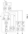
- FIG. 1 illustrates a block diagram of one embodiment of a multi-band front end system 100.
- the illustrated multi-band front end system 100 has the benefit of reducing the number of digital pre-distortion circuitry used per power amplifier.
- Each power amplifier operates in a different transmit band.
- this transmit band is a downlink band.
- the frequency range for a transmit band is also the frequency range of a corresponding receive band.
- Figure 1 illustrates a multi-band front end system 100 configured to transmit and receive on different, e.g. two, transmit bands.
- the illustrated multi-band front system 100 includes a transmitter front end 104 including a first power amplifier 104D and a second power amplifier 104E, and a first receiver front end 106A and a second receiver front end 106B.
- Additional circuitry can be added to facilitate operation on additional transmit and receive band(s). For example, two or more transmitter front end systems can be used; as a result, additional, e.g. three or more, receiver front end systems may also be required.
- a transmitter front end system 104 may include three or more power amplifiers.
- the illustrated fourth duplexer 104C would be replaced by a triplexer.
- a third power amplifier would be coupled to the output of the triplexer.
- an additional coupler and analog to digital converter (ADC) would be added between the output of an additional third power amplifier and a DPD system 104A.
- the third power amplifier, and the additional coupler and ADC would be added in a manner analogous as shown in Figure 1 .
- the illustrated multi-band front end system 100 includes a transmitter front end system 104, a first receiver front end system 106A, a second receiver front end system 106B, a first duplexer 108A, a second duplexer 108B, a third duplexer 108C, and an antenna 110.
- An input of the transmitter front end system 104 is configured to receive digital baseband data or pulse code modulated (i.e. digitized) radio frequency (RF) signals, e.g. from one or more base stations.
- RF radio frequency
- Outputs of the first receiver front end system 106A and the second receiver front end system 106B are respectively configured to provide, e.g. digital baseband data or digitized modulated RF signals.
- the transmitter front end system 104 is configured to receive signals corresponding to the two transmit bands.
- the transmitter bands of the transmitter front end system 104 are widely separated so that the low order intermodulation distortion (IMD) products and harmonics from one transmitter band do not fall within another transmitter band.
- each of the first receiver front end system 106A and the second receiver front end system 106B are configured to operate in, and provide digitized RF signals, in separate receive bands.
- the frequency range of the receive band, the uplink band is different from the frequency range of the transmit band, the downlink band.
- frequency range of the receive band is the same as the frequency range of the transmit band.
- the transmit and receive bands are LTE transmit and receive bands.
- the transmitter front end system 104 and the two receiver front end systems are respectively configured to (a) receive digital baseband data or digitized RF signals, and (b) provide digital baseband data or digitized RF signals. If digital baseband data is provided to and received by respectively the transmitter front end system 104, the first receiver front end system 106A, and the second receiver front end system 106B, then the transmitter front end system 104, the first receiver front end system 106A, and the second receiver front end system 106B must be configured to up convert and down convert transmit and receive signals as will be subsequently described.
- two outputs, respectively corresponding to a first transmit band and a second transmit band, of the transmitter front end system 104 are coupled to first and second ports of a first duplexer 108A.
- An input of the first receiver front end system 106A and an input of the second receiver front end system 106B are respectively coupled to first and second ports of a second duplexer 108B.
- First and second ports of a third duplexer 108C are coupled to third ports of the first duplexer 108A and the second duplexer 108B.
- An antenna 110 is coupled to the third port of the third duplexer 108C.
- the first duplexer 108A, the second duplexer 108B, and/or third duplexer 108C are cavity duplexers.
- the first duplexer 108A, the second duplexer 108B, and/or third duplexer 108C are ceramic duplexers or thin-film bulk acoustic resonators (FBARs).
- Implementations may be used to couple one or more antennas to the output of the transmitter front end system 104, and the inputs of the first receiver front end system 106A and the second receiver front end system 106B.
- the third duplexer 108c and a fifth duplexer could each couple respectively (a) a first port of a first coupler C 1 and the input of first receiver front end system 106A to a first antenna, and (b) a first port of a second coupler C 2 and the input of second receiver front end system 106B to a second antenna.
- the illustrated transmitter front end system 104 comprises the DPD system 104A, a digital to analog converter (DAC) 104B, a fourth duplexer 104C, a first power amplifier (PA) 104D, a second power amplifier 104E, the first coupler C 1 , the second coupler C 2 , a first analog to digital converter (ADC) 104F, and a second ADC 104G.
- the input of the DPD system 104A is configured to receive digital baseband data or digitized RF signals.
- the first ports of the first coupler C 1 and the second coupler C 2 are respectively coupled to the first and second ports of the first duplexer 108A.
- each power amplifier is a monolithic microwave integrated circuit.
- the DPD system 104A modifies signals (which it receives and which correspond to the two transmit bands) to diminish IMD products, typically up to a finite order (e.g. all third and fifth order IMD products).
- the diminished IMD products fall within uplink or receive bands of the multi-band front end system 100, therefore only negligibly decreasing the sensitivity of the multi-band front end system 100 in those uplink bands.
- the reception range of the repeater system (incorporating the multi-band front end system 100) is only negligibly diminished.
- the DPD system 104A generates signals that diminish, e.g. cancel, such IMD products.
- the transmitter front end system 104 is configured to receive digital baseband data.
- the DPD system 104A would modify the digital baseband data to diminish the IMD products in each digitized RF signal at the output of each power amplifier.
- the DPD system 104A could be implemented with the DPD module and coefficient estimator described in the '355 Publication.
- the DAC 104B would include an up converter, e.g. digital up converter proceeding the digital to analog conversion; the first ADC 104F and the second ADC 104G could each include a down converter, e.g. a digital down converter following the analog to digital conversion.
- the DPD system 104A embodies one or more digital pre-distortion circuits to pre-distort signals corresponding to at least two distinct bands; however, the DPD system 104A is implemented in a single device, e.g. such as the devices illustrated below.
- the transmitter front end system 104 is configured to receive a digitized RF signal modulated with data.
- the DPD system 104A would be similarly implemented but would modify the digitized RF signal, e.g. adding RF tones of appropriate amplitude and phase, to suppress the IMD products.
- the DAC and ADCs would not require respectively an up converter and a down converter.
- the data rate and bit rate are respectively reduced to reduce bandwidth (when analog to digital conversion is performed. For pedagogical reasons, Figure 1 will be subsequently described assuming RF signals are provided to the DPD system 104A.
- the DPD system 104A is implemented in any state machine such as a field programmable gate array, a processor such as a digital signal processor (DSP), or an application specific integrated circuit (ASIC).
- the state machine may be coupled to memory, such as programmable read only memory and/or flash memory.
- the DPD system 104A can be implemented in a processing system of another component of the repeater system.
- the DPD system 104A is coupled to an input of the DAC 104B.
- the DAC 104B converts the pre-distorted digitized RF signal, generated from the DPD system 104A, to an analog signal.
- a first port of the fourth duplexer 104C is coupled to the output of the DAC 104B.
- the fourth duplexer 104C filters signals in the first transmit band so that they are provided at a second port of the fourth duplexer 104C, and signals in the second transmit band so that they are provided at a third port of the fourth duplexer 104C.
- the fourth duplexer 104C is implemented with a ceramic or FBAR duplexer; alternatively, the fourth duplexer 104C is implemented with a cavity duplexer.
- the second and third ports of the fourth duplexer 104C are respectively coupled to inputs of the first power amplifier 104D and the second power amplifier 104E.
- the first power amplifier 104D is designed to provide high efficiency power amplification of signals in the first transmit band.
- the second power amplifier 104E is designed to provide high efficiency power amplification of signals in the second transmit band.
- the first power amplifier 104D and the second power amplifier 104E are operated near saturation.
- the first power amplifier 104D and the second power amplifier 104E are coupled in parallel with respect to one another in the illustrated multi-band front end system 100; alternatively, the first power amplifier 104D and the second power amplifier 104E are referred to as a parallel first power amplifier 104D and second power amplifier 104E.
- Second ports of the first coupler C1 and the second coupler C2 are respectively coupled to the outputs of the first power amplifier 104D and the second power amplifier 104E.
- the third ports of the first coupler C1 and the second coupler C2 are respectively coupled to the inputs of the first ADC 104F and the second ADC 104G.
- the first ADC 104F and the second ADC 104G generate digitized signals from the analog signals coupled from the first coupler C1 and the second coupler C2.
- the first coupler C1 and the second coupler C2 are directional couplers.
- the outputs of the first ADC 104F and the second ADC 104G are coupled to the DPD system 104A.
- the DPD system 104A is configured to receive the digitized signals generated by the first ADC 104F and the second ADC 104G and use them to modify the digital baseband data or digitized RF signals so as to diminish IMD products at the output of the first power amplifier 104D and the second power amplifier 104E.
- the digitized signals generated by the first ADC 104F and the second ADC 104G are used to generate frequency components having certain amplitudes and phases necessary to diminish the IMD products.
- the first receiver front end system 106A and the second receiver front end system 106B respectively operate in a first receive band and a second receive band.
- the first receiver front end system 106A comprises a first low noise amplifier (LNA) 106A-1 having an output coupled to an input of a third ADC 106A-2.
- the second receiver front end system 106B comprises a second low noise amplifier (LNA) 106B-1 having an output coupled to an input of a fourth ADC 106B-2.
- each low noise amplifier is a monolithic microwave integrated circuit.
- the DPD system 104 is configured to receive digitized RF signals for two separate transmit bands.
- the DPD system 104 modifies, by pre-distortion, such RF signals, e.g. by adding tones of appropriate amplitude and phase, to diminish IMD products up to a certain order.
- IMD products are generated symmetrically around the center frequency of each transmit band. Because the power levels of higher order IMD products are typically lower than the power levels of lower IMD products, it is only practically necessary to diminish IMD products up to a certain order, e.g. third, fifth or seventh order.
- the pre-distorted RF signals of each transmit band are converted to analog signals by the DAC 104B.
- the analog pre-distorted RF signals of each transmit band are filtered, and thus separated by the fourth duplexer 104C.
- the first power amplifier 104D is configured to receive and power amplify analog pre-distorted RF signals in the first transmit band.
- the second power amplifier 104E is configure to receive and power amplify analog pre-distorted RF signals in the second transmit band. Because of the pre-distortion, the power amplified RF signals, in the first and second transmit bands and provided at the outputs of each of the first power amplifier 104D and the second power amplifier 104E, have diminished IMD products up to the order that the DPD system 104A is designed to diminish.
- the first coupler C1 and the second coupler C2 feedback a portion of the power amplified RF signals in the first and second transmit bands respectively to the first ADC 104F and the second ADC 104G.
- the first ADC 104F and the second ADC 104G which digitize the feedback portions of the power amplified RF signals respectively in the first and second transmit bands.
- the DPD system 104A is configured to receive the digitized feedback portions of the power amplified RF signals respectively in the first and second transmit bands so as to adjust the amplitude and phase of the added tones to enhance the suppression of IMD products.
- the antenna 110 is configured to transmit and receive signals on both sets of transmit and receive bands, e.g. a first band and a second band.
- the first band includes the first downlink band and the first uplink band
- the second band includes the second downlink band and the second uplink band.
- the transmit band and the receive band are a single band, i.e. a transmit band and a receive band having the same frequency range, over which signals are transmitted and received.
- the first duplexer 108A isolates the signals amplified by the first power amplifier 104D and the second power amplifier 104E.
- the second duplexer 108B isolates, e.g . local oscillator signal leakage from, the first receiver front end system 106A and the second receiver front end 106B.
- the third duplexer 108c isolates the first receiver front end system 106A and the second receiver front end system 106B by filtering, or diminishing the amplitude of, signals in the first and second transmit bands emitted by the transmitter front end system 104; this allows avoidance of a reduction of sensitivity in the uplink bands of the receiver of the multi-band front end system 100.
- the RF signals modulated with data in the first uplink band are coupled from the antenna 110, the third duplexer 108c, and the second duplexer 108B to the first receiver front end system 106A.
- a first low noise amplifier 106A-1 is configured to amplify with diminished, e.g. optimized, additive noise so as to diminish, e.g. optimize, the noise figure in the first uplink band of the receiver of the multi-band front end system 100.
- the third ADC 106A-2 digitizes the amplified RF signals in the first receive band.
- the RF signals modulated with data in the second uplink band are coupled from the antenna 110, the third duplexer 108c, and the second duplexer 108B to the second receiver front end system 106B.
- the second low noise amplifier 106B-1 is configured to amplify with diminished, e.g. optimized, additive noise so as to diminish, e.g. optimize, the noise figure in the first uplink band of the receiver of the multi-band front end system 100.
- the fourth ADC 106B-2 digitizes the amplified RF signals in the first receive band.
- the third duplexer 108C diminishes emissions, in the first and the second receive bands, from the transmitter front end system 104 leaking into the first and second receiver front end systems 106A, 106B.
- a relatively high isolation e.g. 120 dB, can be required between the corresponding transmit and receive bands of a duplexer to suppress IMD products (generated in the transmitter front end system 104 and having frequencies in the first and/or second uplink bands) from undesirably diminishing receiver sensitivity.
- Very high isolation duplexers are expensive, increasing system cost. Lower performance, and thus lower cost, duplexers can be used by modifying the operation of the DPD system 104A as described below.
- Transmission and reception respectively over corresponding downlink and uplink bands is referred to as frequency division duplexing.
- the DPD system 104A is designed to diminish IMD products across a bandwidth (or DPD correction bandwidth) that is centered on the center frequency of the downlink band.
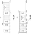
- FIG. 2A illustrates one embodiment of a DPD correction bandwidth 210A.
- the illustrated downlink band is downlink band (DL Band) 66 212DL.
- the DPD correction bandwidth 214 has a center frequency (f c ) 216 of 2155 MHz that is equal to the center frequency of the downlink band 66 212DL.
- f c center frequency
- DL Band 66 212DL and UL Band 66 212UL are not proximate.
- UL Band 66 212UL and part of the UL band 25 are outside of the DPD correction bandwidth 214.
- the third duplexer 108C could be implemented higher isolation between ports one and three (respectively coupled to the transmitter front end system 104, and the first receiver front end system 106A or the second receiver front end system 106B) to diminish higher order IMD products.
- this alternative also undesirably increases system cost.
- FIG. 2B illustrates another embodiment of a DPD correction bandwidth 210B.
- the DPD correction bandwidth 210B has been adjusted to encompass both DL Band 66 212DL and the complete UL frequency range, i.e. UL Band 66 212UL and the complete UL band 25, without increasing the DPD correction bandwidth 210B.
- This technique may also be referred to as skewing the center frequency of the DPD correction bandwidth 210B.
- the center frequency 216 need not be centered about the corresponding downlink and uplink bands so long as both bands fall within the DPD correction bandwidth.
- the downlink band is shown as being higher in frequency than the uplink band, the aforementioned technique also applies when the downlink band is lower in frequency than the uplink band.
- the center frequency of the DPD correction bandwidth 210B can be skewed higher or lower in frequency depending upon the relative position of the corresponding uplink band and the downlink band.
- Skewing of the DPD correction bandwidth 210B can be achieved by reducing the number of (including possibly eliminating) IMD products that are corrected above or below the downlink band, and increasing the number of IMD products that are corrected respectively below or above the downlink band.
- the DPD system 104A diminishes IMD products in the uplink bands of the multiband front end system 100. This skewing technique is utilized with any of the multiband front end systems 100, 300, 400 illustrated in Figures 1 , 3 and 4 .
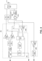
- Figure 3 illustrates a block diagram of another embodiment of a multi-band front end system 300.
- the multi-band front end system 300 includes fewer analog to digital converters than the multi-band front end system 100 illustrated in Figure 1 .
- the implementation and operation of the multi-band front end system 300 illustrated in Figure 3 is otherwise substantially the same as described for the multi-band front end system 100 illustrated in Figure 1 . Differences between the two systems are described below.
- the elements in Figure 3 that are the same as the elements in Figure 1 have the same figure numbers except that those numbers are preceded by a '3' rather than a '1'.
- the transmitter front end system 304 in Figure 3 differs from the transmitter front end system 104 in Figure 1 in that it has one less ADC.
- the third ports of the first coupler C1 and the second coupler C2 are respectively coupled to a first port and a second port of a switch 304H.
- the common port of the switch 304H is coupled to the input of the first ADC 304F.
- the switch 304H is a single pole double throw RF switch.
- One or more control ports of the switch 304H are coupled to the DPD system 304A (as illustrated) and/or another component of the repeater system.
- the control port(s) are configured to select an input port of the switch 304H.
- the DPD system 304A and/or another component include control logic which causes the switch 304H to periodically alternate providing first and second downlink band signals from respectively the second ports of the first coupler C1 and the second coupler C2 to the common port of the switch 304H, and thus to the input of the first ADC 304F.
- the first ADC 304F alternatively digitizes portions of the first and second downlink band signals.
- DPD system 304A includes a switch or other processing circuitry to ensure the digitized downlink band signals are provided to corresponding pre-distortion circuitry affecting the downlink band whose signals are being digitized and provided to the DPD system 304A.
- the control logic and switch 304H replace the more expensive second ADC 104G used in the multi-band front end system 100 of Figure 1 .
- the transmitter front end system 304 may be designed to process more than two downlink bands.
- the switch 304H is a single pole N throw RF switch, where N is the number of switch inputs coupled to the third ports of N couplers.
- a single band i.e. the same frequency range, may be used for both the downlink and uplink band, and employ time division duplexing (TDD).
- TDD repeater systems alternatively transmit and receive in the single band.
- Figure 4 illustrates a block diagram of a further embodiment of a multi-band front end system 400. The illustrated multi-band front end system 400 utilizes TDD on one band.
- a single TDD band is processed by the first power amplifier 404D and the first receiver front end system 406A.
- the first receiver front end system 406A includes the third low noise amplifier 406A-1 (but no third ADC), which has an output coupled to a, e.g. third, port of the switch 404H.
- the aforementioned control logic causes the switch 404H to select the port of the switch 404H coupled to the output of the first receiver front end system 406A when, e.g. the repeater system, is receiving over the single TDD band.
- the received TDD signals, provided at the output of the first receiver front end system 406A are coupled to and digitized by the first ADC 404F.
- the output of the first ADC 404F is coupled to an input of the DPD system 404A.
- a multiplexer (MUX) 404I selectively couples the output of the first ADC 404F between an input of the DPD system 404A and an input of another system, e.g. a downconverter.
- the multiplexer 404I is a switch such as a single pole double throw switch.
- the control logic commands that the multiplexer 404I couple the output of the first ADC 404F to the input of the other system. Otherwise, the control logic commands the multiplexer 404I to couple the output of the first ADC 404F to an input of the DPD system 404A configured to receive a portion of the power amplified RF signals in the first and second transmit bands.
- the control logic causes the switch 404H to periodically alternate providing portions of the power amplified RF signals in the first and second transmit bands (from respectively the third ports of the first coupler C1 and the second coupler C2) to the common port of the switch 404H.
- the alternating portions are then provided to the input of the first ADC 404F.
- the first ADC 404F alternatively digitizes portions of the power amplified RF signals in the first and second transmit bands.
- the multi-band front end system 400 also otherwise differs from the multi-band front end systems 100, 300 of Figures 1 and 3 .
- the second duplexer 108B, 308B of Figures 1 and 3 is replaced by a combiner system 408B.
- the combiner system 408B comprises a circulator 408B-1 and a bandpass filter 408B-2.
- the bandpass filter 408B-2 is designed to only substantially pass signals in the TDD band, and to substantially suppress signals outside of the TDD band.
- first ports of the first coupler C1 and the second coupler C2 are respectively coupled to a first port of a first duplexer 408A and the first port of the combiner system 408B.
- the inputs of the first receiver front end 406A and the second receiver front end 406B are respectively coupled to the second port of the combiner system 408B and the second port of the first duplexer 408A.
- the combiner system 408B couples the output of the second power amplifier 404E and the input to the first receiver front end 406A; both the second power amplifier 404E and the first receiver front end 406A operate in the TDD band.
- the third port of the combiner system 408B is coupled to the second duplexer 408C.
- the duplexer in the transmitter front end 404 is termed the third duplexer 404C.
- the implementation and operation of the multi-band front end system 400 illustrated in Figure 4 is otherwise substantially the same as described for the multi-band front end system 300 illustrated in Figure 3 . Differences between the two systems are described above.
- the elements in Figure 4 that are the same as the elements in Figure 3 have the same figure numbers except that those numbers are preceded by a '4' rather than a '3'.
- Figure 5 illustrates one embodiment of a method of operation of a multi-band front end system 520.
- FIG. 5 illustrates one embodiment of a method of operation of a multi-band front end system 520.
- the blocks of the flow diagrams have been arranged in a generally sequential manner for ease of explanation; however, it is to be understood that this arrangement is merely exemplary, and it should be recognized that the processing associated with the methods (and the blocks shown in the Figures) can occur in a different order (for example, where at least some of the processing associated with the blocks is performed in parallel and/or in an event-driven manner).
- the power amplified, pre-distorted signals are broadcast.
- the signals are digitized RF signals rather than digital baseband signals, then, in another embodiment, convert the digitized RF signals to analog signals prior to power amplification, and digitize the portions of each of the power amplified, pre-distorted signals prior to utilizing them for pre-distortion.
- selectively digitize, with a single ADC the portions of each of the power amplified, pre-distorted signals prior to utilizing them for pre-distortion.
- selectively digitize, with the single analog to digital converter a received signal during a time period for reception.
- skew the center frequency so that the center frequency is equidistant from the center frequencies corresponding to the downlink band, and its corresponding uplink band.
- the DPD techniques and features described above can be implemented in various types of systems.
- the DPD techniques and features described above can be implemented in various types of repeater systems.
- Repeater systems can be implemented in various ways.
- a repeater system can be implemented as a distributed antenna system (DAS).
- DAS distributed antenna system
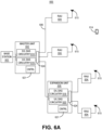
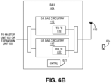
- Figure 6A illustrates one embodiment of a distributed antenna system 600 in which the DPD techniques described above can be implemented.
- the DAS 600 comprises one or more master units 602 that are communicatively coupled to one or more remote antenna units (RAUs) 604 via one or more waveguides 606, e.g. optical fibers or cables.
- RAUs remote antenna units
- Each remote antenna unit 604 can be communicatively coupled directly to one or more of the master units 602 or indirectly via one or more other remote antenna units 604 and/or via one or more expansion (or other intermediary) unit 608.
- the DAS 600 is coupled to one or more base stations 603 and is configured to improve the wireless coverage provided by the base stations 603.
- each base station can be dedicated to the DAS or can be shared among the DAS and a base station antenna system that is co-located with the base station and/or one or more other repeater systems.
- the capacity of one or more base stations 603 are dedicated to the DAS 600 and are co-located with the DAS 600.
- the base stations 603 are coupled to the DAS 600. It is to be understood however that other embodiments can be implemented in other ways.
- the capacity of one or more base stations 603 can be shared with the DAS 600 and a base station antenna system co-located with the base stations 603 (for example, using a donor antenna).
- the base stations 603 can include one or more base stations that are used to provide commercial cellular wireless service and/or one or more base stations that are used to provide public and/or private safety wireless services (for example, wireless communications used by emergency services organizations (such as police, fire and emergency medical services) to prevent or respond to incidents that harm or endanger persons or property).
- emergency services organizations such as police, fire and emergency medical services
- the base stations 603 can be coupled to the master units 602 using a network of attenuators, combiners, splitters, amplifiers, filters, cross-connects, etc., (sometimes referred to collectively as a "point-of-interface" or "POI").
- This network can be included in the master units 602 and/or can be separate from the master units 602. This is done so that, in the downlink, the desired set of RF channels output by the base stations 603 can be extracted, combined, and routed to the appropriate master units 602, and so that, in the upstream, the desired set of carriers output by the master units 602 can be extracted, combined, and routed to the appropriate interface of each base station 603. It is to be understood, however, that this is one example and that other embodiments can be implemented in other ways.
- each master unit 602 comprises downlink DAS circuitry 610 that is configured to receive one or more downlink signals from one or more base stations 603.
- Each base station downlink signal includes one or more radio frequency channels used for communicating in the downlink direction with user equipment 614 over the relevant wireless air interface.
- each base station downlink signal is received as an analog radio frequency signal, though in some embodiments one or more of the base station signals are received in a digital form (for example, in a digital baseband form complying with the Common Public Radio Interface (“CPRI") protocol, Open Radio Equipment Interface (“ORI”) protocol, the Open Base Station Standard Initiative (“OBSAI”) protocol, or other protocol).
- CPRI Common Public Radio Interface
- ORI Open Radio Equipment Interface
- OBSAI Open Base Station Standard Initiative
- the downlink DAS circuitry 610 in each master unit 602 is also configured to generate one or more downlink transport signals derived from one or more base station downlink signals and to transmit one or more downlink transport signals to one or more of the remote antenna units 604.
- each remote antenna unit 604 comprises uplink DAS circuitry 617 that is configured to receive one or more uplink radio frequency signals transmitted from the user equipment 614. These signals are analog radio frequency signals.
- the uplink DAS circuitry 617 in each remote antenna unit 604 is also configured to generate one or more uplink transport signals derived from the one or more remote uplink radio frequency signals and to transmit one or more uplink transport signals to one or more of the master units 602.
- the uplink DAS circuitry 617 of each RAU 604 includes at least one receiver front end (RX FE) 622 which, e.g. amplifies received remote uplink radio frequency signals.
- RX FE receiver front end
- each master unit 602 comprises uplink DAS circuitry 616 that is configured to receive the respective uplink transport signals transmitted to it from one or more remote antenna units 604 and to use the received uplink transport signals to generate one or more base station uplink radio frequency signals that are provided to the one or more base stations 603 associated with that master unit 602.
- uplink DAS circuitry 616 that is configured to receive the respective uplink transport signals transmitted to it from one or more remote antenna units 604 and to use the received uplink transport signals to generate one or more base station uplink radio frequency signals that are provided to the one or more base stations 603 associated with that master unit 602.
- this involves, among other things, combining or summing uplink signals received from multiple remote antenna units 604 in order to produce the base station signal provided to each base station 603.
- the DAS 600 increases the coverage area for the uplink capacity provided by the base stations 603.
- Each expansion unit 608 comprises downlink DAS circuitry (D/L DAS circuitry) 618 that is configured to receive the downlink transport signals transmitted to it from the master unit 602 (or other expansion unit 608) and transmits the downlink transport signals to one or more remote antenna units 604 or other downstream expansion units 608.
- Each expansion unit 608 also comprises uplink DAS circuitry 620 that is configured to receive the respective uplink transport signals transmitted to it from one or more remote antenna units 604 or other downstream expansion units 608, combine or sum the received uplink transport signals, and transmit the combined uplink transport signals upstream to the master unit 602 or other expansion unit 608.
- one or more remote antenna units 604 are coupled to one or more master units 602 via one or more other remote antenna units 604 (for example, where the remote antenna units 604 are coupled together in a daisy chain or ring topology).
- the downlink DAS circuitry (D/L DAS circuitry) 610, 612, and 618 and uplink DAS circuitry (U/L DAS circuitry) 616, 617, and 620 in each master unit 602, remote antenna unit 604, and expansion unit 608, respectively, can comprise one or more appropriate connectors, attenuators, combiners, splitters, amplifiers, filters, duplexers, analog-to-digital converters, digital-to-analog converters, electrical-to-optical converters, optical-to-electrical converters, mixers, field-programmable gate arrays (FPGAs), microprocessors, transceivers, framers, etc., to implement the features described above. Also, the downlink DAS circuitry 610, 612, and 618 and uplink DAS circuitry 616, 617, and 620 may share common circuitry and/or components.
- the DAS 600 can use either digital transport, analog transport, or combinations of digital and analog transport for generating and communicating the transport signals between the master units 602, the remote antenna units 604, and any expansion units 608.
- Each master unit 602, remote antenna unit 604, and expansion unit 608 in the DAS 600 also comprises a respective controller (CNTRL) 621.
- the controller 621 is implemented using one or more programmable processors that execute software that is configured to implement the various control functions.
- the controller 621 (more specifically, the various control functions implemented by the controller 621) (or portions thereof) can be implemented in other ways (for example, in a field programmable gate array (FPGA), application specific integrated circuit (ASIC), etc.).
- the DPD system 404A and/or control logic described above may be incorporated in, e.g. the controller 621 of a remote antenna unit 604 or in another controller 621 or state machine incorporated into the distributed antenna system 600.
- the at least one transmitter front end 619 includes at least one of the transmitter front ends 104, 304, 404 described above.
- the at least one receiver front end 622 includes at least one, e.g. two, of the corresponding receiver front ends 106A, 106B, 306A, 306B, 406A, 406B described above.
- a combination of two or more duplexers and/or one or more duplexers and one or more combiner systems can be used to couple the at least one transmitter front end 619 and the at least one receiver front end 622 to one or more antennas 615.
- the DPD system 104A, 304A, 404A and/or control logic may be incorporated, e.g. in the controller 621 of a remote antenna unit 604 or in another controller 621 otherwise incorporated into the distributed antenna system 600.
- Repeater systems can be implemented in other ways.
- a repeater system can be implemented as a single-node repeater.
- Figure 7 illustrates one embodiment of a single-node repeater 700 in which the DPD techniques described above can be implemented.
- the single-node repeater 700 comprises downlink repeater circuitry 712 that is configured to receive one or more downlink signals from one or more base stations 703. These signals are also referred to here as "base station downlink signals.” Each base station downlink signal includes one or more radio frequency channels used for communicating in the downlink direction with user equipment (UE) 714 over the relevant wireless air interface. Typically, each base station downlink signal is received as an analog radio frequency signal.
- UE user equipment
- the downlink repeater circuitry 712 in the single-node repeater 700 is also configured to generate one or more downlink radio frequency signals that are radiated from one or more antennas 715 associated with the single-node repeater 700 for reception by user equipment 714.
- These downlink radio frequency signals are analog radio frequency signals and are also referred to here as "repeated downlink radio frequency signals.”
- Each repeated downlink radio frequency signal includes one or more of the downlink radio frequency channels used for communicating with user equipment 714 over the wireless air interface.
- the single-node repeater 700 is an active repeater system in which the downlink repeater circuitry 712 comprises one or more amplifiers (or other gain elements) that are used to control and adjust the gain of the repeated downlink radio frequency signals radiated from the one or more antennas 715.
- the downlink repeater circuitry 712 includes at least one transmitter front end (TX FE) 719 which, for example, power amplifies the repeated downlink radio frequency signals.
- TX FE transmitter front end
- the single-node repeater 700 comprises uplink repeater circuitry 720 that is configured to receive one or more uplink radio frequency signals transmitted from the user equipment 714. These signals are analog radio frequency signals and are also referred to here as "UE uplink radio frequency signals.” Each UE uplink radio frequency signal includes one or more radio frequency channels used for communicating in the uplink direction with user equipment 714 over the relevant wireless air interface.
- the uplink repeater circuitry 720 in the single-node repeater 700 is also configured to generate one or more uplink radio frequency signals that are provided to the one or more base stations 703. These signals are also referred to here as "repeated uplink signals.” Each repeated uplink signal includes one or more of the uplink radio frequency channels used for communicating with user equipment 714 over the wireless air interface.
- the single-node repeater 700 is an active repeater system in which the uplink repeater circuitry 720 comprises one or more amplifiers (or other gain elements) that are used to control and adjust the gain of the repeated uplink radio frequency signals provided to the one or more base stations 703.
- each repeated uplink signal is provided to the one or more base stations 703 as an analog radio frequency signal.
- the uplink repeater circuitry 720 includes at least one receiver front end (RX FE) 722 which, e.g., amplifies received uplink radio frequency signals.
- RX FE receiver front end
- the downlink repeater circuitry 712 and uplink repeater circuitry 720 can comprise one or more appropriate connectors, attenuators, combiners, splitters, amplifiers, filters, duplexers, analog-to-digital converters, digital-to-analog converters, electrical-to-optical converters, optical-to-electrical converters, mixers, field-programmable gate arrays (FPGAs), microprocessors, transceivers, framers, etc., to implement the features described above. Also, the downlink repeater circuitry 712 and uplink repeater circuitry 720 may share common circuitry and/or components.
- the at least one transmitter front end 719 includes at least one of the transmitter front ends 104, 304, 404 described above.
- the at least one receiver front end 722 includes at least one, e.g. two, of the corresponding receiver front ends 106A, 106B, 306A, 306B, 406A, 406B described above. Further a combination of two or more duplexers can be used to couple the at least one transmitter front end 719 and the at least one receiver front end 722 to one or more antennas 715.
- the single-node repeater system 700 also comprises a controller (CNTRL) 721.
- the controller 721 is implemented using one or more programmable processors that execute software that is configured to implement the various control functions.
- the controller 721 (more specifically, the various control functions implemented by the controller 721) (or portions thereof) can be implemented in other ways (for example, in a field programmable gate array (FPGA), application specific integrated circuit (ASIC), etc.).
- the DPD system 104A, 304A, 404A and/or control logic may be incorporated, e.g. in the controller 721 of the single-node repeater system 700.
- a signal may be a voltage signal or a current signal.
Landscapes
- Engineering & Computer Science (AREA)
- Power Engineering (AREA)
- Computer Networks & Wireless Communication (AREA)
- Signal Processing (AREA)
- Physics & Mathematics (AREA)
- Nonlinear Science (AREA)
- Transceivers (AREA)
- Amplifiers (AREA)
Claims (7)
- Multiband-Frontend-System, umfassend:ein digitales Vorverzerrungssystem (DPD) (104A, 304A, 404A), das einen Eingang, der dazu konfiguriert ist, Signale zu empfangen, die mindestens zwei Sendebändern entsprechen, und einen Ausgang umfasst;einen Digital-Analog-Wandler (104B, 304B, 404B), der einen Eingang, der mit dem Ausgang des DPD-Systems gekoppelt ist, und einen Ausgang umfasst;einen ersten Multiplexer (104C, 304C, 404C), der einen ersten Anschluss, einen zweiten Anschluss und einen dritten Anschluss umfasst, wobei der erste Anschluss mit dem Ausgang des Digital-Analog-Wandlers gekoppelt ist, wobei ein Multiplexer dazu konfiguriert ist, zwei oder mehr Bänder zu filtern/zusammenzufassen oder aufzuteilen;einen ersten Leistungsverstärker (104D, 304D, 404D), der einen mit dem zweiten Anschluss des ersten Multiplexers gekoppelten Eingang und einen Ausgang umfasst und dazu konfiguriert ist, Signale in einem ersten Sendeband leistungszuverstärken;einen zweiten Leistungsverstärker (104E, 304E, 404E), der einen mit dem dritten Anschluss des ersten Multiplexers gekoppelten Eingang und einen Ausgang umfasst und dazu konfiguriert ist, Signale in einem zweiten Sendeband leistungszuverstärken;einen ersten Koppler (C1), der einen ersten Anschluss, einen zweiten Anschluss und einen dritten Anschluss umfasst, wobei der erste Anschluss des ersten Kopplers mit dem Ausgang des ersten Leistungsverstärkers gekoppelt ist;einen zweiten Koppler (C2), der einen ersten Anschluss, einen zweiten Anschluss und einen dritten Anschluss umfasst, wobei der erste Anschluss des zweiten Kopplers mit dem Ausgang des zweiten Leistungsverstärkers gekoppelt ist; undeines von:(a) einen ersten Analog-Digital-Wandler (104F), der einen Eingang umfasst, der mitdem zweiten Anschluss des ersten Kopplers und einem Ausgang gekoppelt ist, der mit dem DPD-System gekoppelt ist; undeinem zweiten Analog-Digital-Wandler (104G), der einen mit dem zweiten Anschluss des zweiten Kopplers gekoppelten Eingang und einen mit dem DPD-System gekoppelten Ausgang umfasst; oder(b) einen Schalter (304H, 404H), der einen ersten Eingangsanschluss umfasst, der mit dem zweiten Anschluss des ersten Kopplers gekoppelt ist, einen zweiten Eingangsanschluss, der mit dem zweiten Anschluss des zweiten Kopplers gekoppelt ist, einen gemeinsamen Anschluss und mindestens einen Steueranschluss, der mit dem DPD-System gekoppelt und dazu konfiguriert ist, einen Eingangsanschluss des Schalters auszuwählen; undeinen dritten Analog-Digital-Wandler (304F, 404F), umfassend einen Eingang, der mit dem gemeinsamen Anschluss des Schalters gekoppelt ist, und einen Ausgang, der mit dem DPD-System gekoppelt ist;wobei das DPD-System dazu konfiguriert ist, eine Mittenfrequenz (216) einer Bandbreite (214), in der eine Vorverzerrung durchgeführt wird und die einem der mindestens zwei Sendebänder entspricht, zu verzerren, sodass eine Vorverzerrungsbandbreite entsprechende Uplink- und Downlink-Bänder abdeckt und Intermodulationsverzerrungsprodukte in der Vorverzerrungsbandbreite verringert werden.
- System nach Anspruch 1, wobei die Mittenfrequenz von den Mittenfrequenzen, die den entsprechenden Uplink- und Downlink-Bändern entsprechen, äquidistant ist.
- Verfahren unter Verwendung des Systems nach Anspruch 1, umfassend:Leistungsverstärkung (522), unter Verwendung des ersten und des zweiten Leistungsverstärkers, von mindestens zwei vorverzerrten Signalen, von denen jedes einem eindeutigen Sendeband entspricht, wobei jeder Leistungsverstärker in einem eindeutigen Sendeband arbeitet;Vorverzerrung (524), mit dem DPD-System, von mindestens zwei Signalen in unterschiedlichen Sendebändern, wobei die Vorverzerrung jedes der mindestens zwei Signale auf einem Teil eines entsprechenden leistungsverstärkten, vorverzerrten Signals basiert; undVerzerren (526), mit dem DPD-System, der Mittenfrequenz der Bandbreite, in der die Vorverzerrung durchgeführt wird und die einem Sendeband entspricht, sodass eine Vorverzerrungsbandbreite die entsprechenden Uplink- und Downlink-Bänder abdeckt, wobei die Vorverzerrung Intermodulationsverzerrungsprodukte in der Vorverzerrungsbandbreite verringert.
- Verfahren nach Anspruch 3, wobei, wenn die mindestens zwei Signale digitale Basisbanddaten sind, vor der Leistungsverstärkung vorverzerrte Signale aufwärts konvertiert werden und vor der Verwendung der Abschnitte der leistungsverstärkten, vorverzerrten Signale zur Vorverzerrung Abschnitte der leistungsverstärkten, vorverzerrten Signale nach unten konvertiert werden.
- Verfahren nach Anspruch 3, wobei, wenn vorverzerrte Signale vor der Leistungsverstärkung digitale Signale sind, die digitalen Signale vor der Leistungsverstärkung in analoge Signale konvertiert werden und Abschnitte jedes der leistungsverstärkten, vorverzerrten Signale vor der Verwendung der Abschnitte jedes der leistungsverstärkten vorverzerrten Signale zur Vorverzerrung digitalisiert werden.
- Verfahren nach Anspruch 5, wobei das Digitalisieren der Abschnitte das selektive Digitalisieren der Abschnitte jedes der leistungsverstärkten, vorverzerrten Signale mit dem dritten Analog-Digital-Wandler vor dem Verwenden der Abschnitte jedes der leistungsverstärkten, vorverzerrten Signale zur Vorverzerrung umfasst.
- Verfahren nach Anspruch 6, wobei das selektive Digitalisieren, mit dem dritten Analog-Digital-Wandler, ferner umfasst, dass, wenn ein eindeutiges Sendeband zum Zeitduplexen verwendet wird, ein empfangenes Signal während einer Zeitperiode zum Empfangen selektiv mit dem dritten Analog-Digital-Wandler digitalisiert wird.
Priority Applications (1)
| Application Number | Priority Date | Filing Date | Title |
|---|---|---|---|
| EP24208123.0A EP4472083A3 (de) | 2017-08-10 | 2018-07-31 | Verfahren und vorrichtungen zur digitalen vorverzerrung |
Applications Claiming Priority (2)
| Application Number | Priority Date | Filing Date | Title |
|---|---|---|---|
| US201762543453P | 2017-08-10 | 2017-08-10 | |
| PCT/US2018/044585 WO2019032337A1 (en) | 2017-08-10 | 2018-07-31 | METHODS AND APPARATUSES FOR DIGITAL PRE-DISTORTION |
Related Child Applications (2)
| Application Number | Title | Priority Date | Filing Date |
|---|---|---|---|
| EP24208123.0A Division-Into EP4472083A3 (de) | 2017-08-10 | 2018-07-31 | Verfahren und vorrichtungen zur digitalen vorverzerrung |
| EP24208123.0A Division EP4472083A3 (de) | 2017-08-10 | 2018-07-31 | Verfahren und vorrichtungen zur digitalen vorverzerrung |
Publications (3)
| Publication Number | Publication Date |
|---|---|
| EP3665880A1 EP3665880A1 (de) | 2020-06-17 |
| EP3665880A4 EP3665880A4 (de) | 2022-01-05 |
| EP3665880B1 true EP3665880B1 (de) | 2025-04-30 |
Family
ID=65272398
Family Applications (2)
| Application Number | Title | Priority Date | Filing Date |
|---|---|---|---|
| EP18845197.5A Active EP3665880B1 (de) | 2017-08-10 | 2018-07-31 | Verfahren und vorrichtungen zur digitalen vorverzerrung |
| EP24208123.0A Pending EP4472083A3 (de) | 2017-08-10 | 2018-07-31 | Verfahren und vorrichtungen zur digitalen vorverzerrung |
Family Applications After (1)
| Application Number | Title | Priority Date | Filing Date |
|---|---|---|---|
| EP24208123.0A Pending EP4472083A3 (de) | 2017-08-10 | 2018-07-31 | Verfahren und vorrichtungen zur digitalen vorverzerrung |
Country Status (4)
| Country | Link |
|---|---|
| US (3) | US10615754B2 (de) |
| EP (2) | EP3665880B1 (de) |
| CN (1) | CN110999234B (de) |
| WO (1) | WO2019032337A1 (de) |
Families Citing this family (13)
| Publication number | Priority date | Publication date | Assignee | Title |
|---|---|---|---|---|
| US10615754B2 (en) | 2017-08-10 | 2020-04-07 | Commscope Technologies Llc | Methods and apparatuses for digital pre-distortion |
| KR102554666B1 (ko) * | 2018-09-21 | 2023-07-13 | 삼성전자주식회사 | 안테나로부터 수신되는 신호에 기반하여 통신 회로를 제어하는 전자 장치 |
| JP6919664B2 (ja) * | 2019-01-31 | 2021-08-18 | 株式会社村田製作所 | マルチプレクサおよび通信装置 |
| US10735095B1 (en) * | 2019-03-04 | 2020-08-04 | Advanced Rf Technologies, Inc. | Distributed antenna system for massive MIMO signals with one fiber optic cable |
| JP2020205472A (ja) * | 2019-06-14 | 2020-12-24 | 株式会社村田製作所 | 高周波回路および通信装置 |
| KR20210108196A (ko) * | 2020-02-25 | 2021-09-02 | 주식회사 케이엠더블유 | 멀티 밴드 송신기 |
| US11329688B2 (en) | 2020-03-18 | 2022-05-10 | Commscope Technologies Llc | Single-chip digital pre-distortion (DPD) device implemented using radio frequency transceiver integrated circuit with integrated DPD function |
| CN112332788B (zh) * | 2020-10-22 | 2024-07-02 | 浙江三维利普维网络有限公司 | 一种射频功放模块 |
| US12034470B2 (en) * | 2020-11-02 | 2024-07-09 | Nokia Solutions And Networks Oy | Radio apparatus |
| US11901921B2 (en) * | 2020-11-02 | 2024-02-13 | Nokia Solutions And Networks Oy | Radio apparatus |
| US12476663B2 (en) | 2021-06-17 | 2025-11-18 | Outdoor Wireless Networks LLC | Systems and methods for multi-transceiver radio frequency signal processing systems |
| CN114448454B (zh) * | 2021-12-28 | 2024-05-10 | 西安邮电大学 | 一种可抑制谐波和互调失真的短波发射机 |
| WO2025156161A1 (zh) * | 2024-01-24 | 2025-07-31 | 深圳高性能医疗器械国家研究院有限公司 | 多核成像射频功率放大器以及多核磁共振成像硬件系统 |
Family Cites Families (23)
| Publication number | Priority date | Publication date | Assignee | Title |
|---|---|---|---|---|
| JPH10290125A (ja) * | 1997-04-15 | 1998-10-27 | Hitachi Denshi Ltd | 電力増幅器 |
| US6944238B2 (en) * | 2001-02-16 | 2005-09-13 | Lucent Technologies Inc. | Digital transmitter system and method |
| US7058369B1 (en) * | 2001-11-21 | 2006-06-06 | Pmc-Sierra Inc. | Constant gain digital predistortion controller for linearization of non-linear amplifiers |
| US20060040624A1 (en) * | 2002-12-20 | 2006-02-23 | Dietmar Lipka | Peak power limitation in an amplifier pooling scenario |
| JP4576221B2 (ja) * | 2004-02-03 | 2010-11-04 | 株式会社エヌ・ティ・ティ・ドコモ | 多周波帯用べき級数型プリディストータ |
| US7541868B2 (en) * | 2007-05-31 | 2009-06-02 | Andrew, Llc | Delay modulator pre-distortion circuit for an amplifier |
| KR101433845B1 (ko) * | 2008-01-23 | 2014-08-27 | 삼성전자주식회사 | 다중 안테나 무선통신 시스템에서 피드백 경로를 공유하는디지털 선 왜곡 장치 및 방법 |
| KR20110002020A (ko) | 2008-03-12 | 2011-01-06 | 하이프레스 인코포레이티드 | 디지털 rf 트랜시버 시스템 및 방법 |
| CN101594327B (zh) * | 2008-05-26 | 2012-06-13 | 芯通科技(成都)有限公司 | 多通道数字预失真处理装置及预失真处理方法 |
| US8265572B2 (en) * | 2009-12-21 | 2012-09-11 | Ubidyne, Inc. | Multiple envelope tracking system for an active antenna array |
| WO2011105359A1 (ja) * | 2010-02-24 | 2011-09-01 | 住友電気工業株式会社 | 増幅装置、信号処理装置、無線通信装置、コネクタ取付構造、及び同軸コネクタ |
| US8355682B2 (en) * | 2010-10-05 | 2013-01-15 | Ubidyne, Inc. | Radio transmitter and method for transmission of combined signal |
| US9184710B2 (en) | 2011-02-09 | 2015-11-10 | Intel Corporation | Digital predistortion of a power amplifier for signals comprising widely spaced carriers |
| US8964821B2 (en) * | 2011-10-14 | 2015-02-24 | Qualcomm Incorporated | Shared feedback for adaptive transmitter pre-distortion |
| US20130109326A1 (en) * | 2011-10-28 | 2013-05-02 | Broadcom Corporation | Rf transceiver with calibrated pre-distortion and methods for use therewith |
| EP2654210B1 (de) * | 2012-04-16 | 2014-05-14 | Alcatel Lucent | Nebensprechauflösung in einem Multibandsendeempfänger |
| US8913689B2 (en) | 2012-09-24 | 2014-12-16 | Dali Systems Co. Ltd. | Wide bandwidth digital predistortion system with reduced sampling rate |
| US9172334B2 (en) * | 2013-05-09 | 2015-10-27 | King Fahd University Of Petroleum And Minerals | Digital predistortion system and method with extended correction bandwidth |
| US9385762B2 (en) * | 2013-05-22 | 2016-07-05 | Telefonaktiebolaget L M Ericsson (Publ) | Linearization of intermodulation bands for concurrent dual-band power amplifiers |
| EP3018874B1 (de) * | 2013-12-23 | 2018-05-23 | Huawei Technologies Co., Ltd. | Drahtloser senderempfänger |
| US10079702B2 (en) * | 2015-07-06 | 2018-09-18 | Mediatek Singapore Pte. Ltd. | Front-end module and coupling compensation for closed-loop digital pre-distortion system |
| US9825657B2 (en) * | 2016-01-12 | 2017-11-21 | Google Inc. | Digital pre-distortion linearization for mobile communication |
| US10615754B2 (en) | 2017-08-10 | 2020-04-07 | Commscope Technologies Llc | Methods and apparatuses for digital pre-distortion |
-
2018
- 2018-07-31 US US16/050,740 patent/US10615754B2/en active Active
- 2018-07-31 WO PCT/US2018/044585 patent/WO2019032337A1/en not_active Ceased
- 2018-07-31 EP EP18845197.5A patent/EP3665880B1/de active Active
- 2018-07-31 CN CN201880052755.2A patent/CN110999234B/zh active Active
- 2018-07-31 EP EP24208123.0A patent/EP4472083A3/de active Pending
-
2020
- 2020-02-24 US US16/799,018 patent/US10998865B2/en not_active Ceased
-
2023
- 2023-04-24 US US18/138,436 patent/USRE50175E1/en active Active
Also Published As
| Publication number | Publication date |
|---|---|
| EP3665880A1 (de) | 2020-06-17 |
| EP3665880A4 (de) | 2022-01-05 |
| CN110999234A (zh) | 2020-04-10 |
| EP4472083A2 (de) | 2024-12-04 |
| USRE50175E1 (en) | 2024-10-15 |
| US10998865B2 (en) | 2021-05-04 |
| EP4472083A3 (de) | 2025-02-26 |
| CN110999234B (zh) | 2022-08-30 |
| WO2019032337A1 (en) | 2019-02-14 |
| US20200195203A1 (en) | 2020-06-18 |
| US10615754B2 (en) | 2020-04-07 |
| US20190052234A1 (en) | 2019-02-14 |
Similar Documents
| Publication | Publication Date | Title |
|---|---|---|
| EP3665880B1 (de) | Verfahren und vorrichtungen zur digitalen vorverzerrung | |
| US10601378B2 (en) | Distributed antenna system architectures | |
| US11283530B2 (en) | Wideband remote unit for distributed antenna system | |
| EP3531565B1 (de) | Turmspitzenvorrichtung und verfahren zur unterdrückung von passiver intermodulation | |
| JP5603950B2 (ja) | アンテナ素子の多重化方法および多重化装置、ならびにアンテナ構成要素 | |
| US12224837B2 (en) | Systems and methods for reconfigurable repeaters for wireless telecommunications | |
| US12476663B2 (en) | Systems and methods for multi-transceiver radio frequency signal processing systems | |
| EP3289688B1 (de) | Non-duplexer-architekturen für telekommunikationssystem | |
| WO2016027134A1 (en) | Feedback transmitter and receiver sharing | |
| KR101182035B1 (ko) | 복수안테나를 구비한 원격 기지국 유닛 및 양방향 광 무선네트워크 | |
| KR101168015B1 (ko) | Iss 필터 모듈을 응용한 유무선통신장치 | |
| KR101431528B1 (ko) | 전대역 듀플렉서 및 그를 위한 무선 통신 시스템 |
Legal Events
| Date | Code | Title | Description |
|---|---|---|---|
| STAA | Information on the status of an ep patent application or granted ep patent |
Free format text: STATUS: THE INTERNATIONAL PUBLICATION HAS BEEN MADE |
|
| PUAI | Public reference made under article 153(3) epc to a published international application that has entered the european phase |
Free format text: ORIGINAL CODE: 0009012 |
|
| STAA | Information on the status of an ep patent application or granted ep patent |
Free format text: STATUS: REQUEST FOR EXAMINATION WAS MADE |
|
| 17P | Request for examination filed |
Effective date: 20200227 |
|
| AK | Designated contracting states |
Kind code of ref document: A1 Designated state(s): AL AT BE BG CH CY CZ DE DK EE ES FI FR GB GR HR HU IE IS IT LI LT LU LV MC MK MT NL NO PL PT RO RS SE SI SK SM TR |
|
| AX | Request for extension of the european patent |
Extension state: BA ME |
|
| DAV | Request for validation of the european patent (deleted) | ||
| DAX | Request for extension of the european patent (deleted) | ||
| RIC1 | Information provided on ipc code assigned before grant |
Ipc: H03M 1/12 20060101ALI20210825BHEP Ipc: H04L 25/02 20060101ALI20210825BHEP Ipc: H04L 25/49 20060101ALI20210825BHEP Ipc: H03F 1/32 20060101AFI20210825BHEP |
|
| REG | Reference to a national code |
Ref country code: DE Ref legal event code: R079 Free format text: PREVIOUS MAIN CLASS: H04L0025490000 Ipc: H03F0001320000 Ref document number: 602018081589 Country of ref document: DE |
|
| A4 | Supplementary search report drawn up and despatched |
Effective date: 20211206 |
|
| RIC1 | Information provided on ipc code assigned before grant |
Ipc: H03M 1/12 20060101ALI20211130BHEP Ipc: H04L 25/02 20060101ALI20211130BHEP Ipc: H04L 25/49 20060101ALI20211130BHEP Ipc: H03F 1/32 20060101AFI20211130BHEP |
|
| RAP3 | Party data changed (applicant data changed or rights of an application transferred) |
Owner name: COMMSCOPE TECHNOLOGIES LLC |
|
| GRAP | Despatch of communication of intention to grant a patent |
Free format text: ORIGINAL CODE: EPIDOSNIGR1 |
|
| STAA | Information on the status of an ep patent application or granted ep patent |
Free format text: STATUS: GRANT OF PATENT IS INTENDED |
|
| INTG | Intention to grant announced |
Effective date: 20240625 |
|
| RAP1 | Party data changed (applicant data changed or rights of an application transferred) |
Owner name: OUTDOOR WIRELESS NETWORKS LLC |
|
| GRAJ | Information related to disapproval of communication of intention to grant by the applicant or resumption of examination proceedings by the epo deleted |
Free format text: ORIGINAL CODE: EPIDOSDIGR1 |
|
| STAA | Information on the status of an ep patent application or granted ep patent |
Free format text: STATUS: REQUEST FOR EXAMINATION WAS MADE |
|
| INTC | Intention to grant announced (deleted) | ||
| GRAP | Despatch of communication of intention to grant a patent |
Free format text: ORIGINAL CODE: EPIDOSNIGR1 |
|
| STAA | Information on the status of an ep patent application or granted ep patent |
Free format text: STATUS: GRANT OF PATENT IS INTENDED |
|
| INTG | Intention to grant announced |
Effective date: 20241203 |
|
| GRAS | Grant fee paid |
Free format text: ORIGINAL CODE: EPIDOSNIGR3 |
|
| GRAA | (expected) grant |
Free format text: ORIGINAL CODE: 0009210 |
|
| STAA | Information on the status of an ep patent application or granted ep patent |
Free format text: STATUS: THE PATENT HAS BEEN GRANTED |
|
| AK | Designated contracting states |
Kind code of ref document: B1 Designated state(s): AL AT BE BG CH CY CZ DE DK EE ES FI FR GB GR HR HU IE IS IT LI LT LU LV MC MK MT NL NO PL PT RO RS SE SI SK SM TR |
|
| REG | Reference to a national code |
Ref country code: CH Ref legal event code: EP Ref country code: GB Ref legal event code: FG4D |
|
| REG | Reference to a national code |
Ref country code: DE Ref legal event code: R096 Ref document number: 602018081589 Country of ref document: DE |
|
| REG | Reference to a national code |
Ref country code: IE Ref legal event code: FG4D |
|
| REG | Reference to a national code |
Ref country code: NL Ref legal event code: MP Effective date: 20250430 |
|
| REG | Reference to a national code |
Ref country code: AT Ref legal event code: MK05 Ref document number: 1791046 Country of ref document: AT Kind code of ref document: T Effective date: 20250430 |
|
| PG25 | Lapsed in a contracting state [announced via postgrant information from national office to epo] |
Ref country code: PT Free format text: LAPSE BECAUSE OF FAILURE TO SUBMIT A TRANSLATION OF THE DESCRIPTION OR TO PAY THE FEE WITHIN THE PRESCRIBED TIME-LIMIT Effective date: 20250901 Ref country code: FI Free format text: LAPSE BECAUSE OF FAILURE TO SUBMIT A TRANSLATION OF THE DESCRIPTION OR TO PAY THE FEE WITHIN THE PRESCRIBED TIME-LIMIT Effective date: 20250430 Ref country code: ES Free format text: LAPSE BECAUSE OF FAILURE TO SUBMIT A TRANSLATION OF THE DESCRIPTION OR TO PAY THE FEE WITHIN THE PRESCRIBED TIME-LIMIT Effective date: 20250430 |
|
| PGFP | Annual fee paid to national office [announced via postgrant information from national office to epo] |
Ref country code: DE Payment date: 20250730 Year of fee payment: 8 |
|
| REG | Reference to a national code |
Ref country code: LT Ref legal event code: MG9D |
|
| PG25 | Lapsed in a contracting state [announced via postgrant information from national office to epo] |
Ref country code: NO Free format text: LAPSE BECAUSE OF FAILURE TO SUBMIT A TRANSLATION OF THE DESCRIPTION OR TO PAY THE FEE WITHIN THE PRESCRIBED TIME-LIMIT Effective date: 20250730 Ref country code: GR Free format text: LAPSE BECAUSE OF FAILURE TO SUBMIT A TRANSLATION OF THE DESCRIPTION OR TO PAY THE FEE WITHIN THE PRESCRIBED TIME-LIMIT Effective date: 20250731 |
|
| PG25 | Lapsed in a contracting state [announced via postgrant information from national office to epo] |
Ref country code: NL Free format text: LAPSE BECAUSE OF FAILURE TO SUBMIT A TRANSLATION OF THE DESCRIPTION OR TO PAY THE FEE WITHIN THE PRESCRIBED TIME-LIMIT Effective date: 20250430 Ref country code: PL Free format text: LAPSE BECAUSE OF FAILURE TO SUBMIT A TRANSLATION OF THE DESCRIPTION OR TO PAY THE FEE WITHIN THE PRESCRIBED TIME-LIMIT Effective date: 20250430 |
|
| PG25 | Lapsed in a contracting state [announced via postgrant information from national office to epo] |
Ref country code: BG Free format text: LAPSE BECAUSE OF FAILURE TO SUBMIT A TRANSLATION OF THE DESCRIPTION OR TO PAY THE FEE WITHIN THE PRESCRIBED TIME-LIMIT Effective date: 20250430 |
|
| PG25 | Lapsed in a contracting state [announced via postgrant information from national office to epo] |
Ref country code: HR Free format text: LAPSE BECAUSE OF FAILURE TO SUBMIT A TRANSLATION OF THE DESCRIPTION OR TO PAY THE FEE WITHIN THE PRESCRIBED TIME-LIMIT Effective date: 20250430 |
|
| PG25 | Lapsed in a contracting state [announced via postgrant information from national office to epo] |
Ref country code: AT Free format text: LAPSE BECAUSE OF FAILURE TO SUBMIT A TRANSLATION OF THE DESCRIPTION OR TO PAY THE FEE WITHIN THE PRESCRIBED TIME-LIMIT Effective date: 20250430 |
|
| PG25 | Lapsed in a contracting state [announced via postgrant information from national office to epo] |
Ref country code: RS Free format text: LAPSE BECAUSE OF FAILURE TO SUBMIT A TRANSLATION OF THE DESCRIPTION OR TO PAY THE FEE WITHIN THE PRESCRIBED TIME-LIMIT Effective date: 20250731 |
|
| PG25 | Lapsed in a contracting state [announced via postgrant information from national office to epo] |
Ref country code: IS Free format text: LAPSE BECAUSE OF FAILURE TO SUBMIT A TRANSLATION OF THE DESCRIPTION OR TO PAY THE FEE WITHIN THE PRESCRIBED TIME-LIMIT Effective date: 20250830 |
|
| PG25 | Lapsed in a contracting state [announced via postgrant information from national office to epo] |
Ref country code: LV Free format text: LAPSE BECAUSE OF FAILURE TO SUBMIT A TRANSLATION OF THE DESCRIPTION OR TO PAY THE FEE WITHIN THE PRESCRIBED TIME-LIMIT Effective date: 20250430 |
|
| PG25 | Lapsed in a contracting state [announced via postgrant information from national office to epo] |
Ref country code: DK Free format text: LAPSE BECAUSE OF FAILURE TO SUBMIT A TRANSLATION OF THE DESCRIPTION OR TO PAY THE FEE WITHIN THE PRESCRIBED TIME-LIMIT Effective date: 20250430 Ref country code: SM Free format text: LAPSE BECAUSE OF FAILURE TO SUBMIT A TRANSLATION OF THE DESCRIPTION OR TO PAY THE FEE WITHIN THE PRESCRIBED TIME-LIMIT Effective date: 20250430 |
|
| PG25 | Lapsed in a contracting state [announced via postgrant information from national office to epo] |
Ref country code: CZ Free format text: LAPSE BECAUSE OF FAILURE TO SUBMIT A TRANSLATION OF THE DESCRIPTION OR TO PAY THE FEE WITHIN THE PRESCRIBED TIME-LIMIT Effective date: 20250430 |
|
| PG25 | Lapsed in a contracting state [announced via postgrant information from national office to epo] |
Ref country code: EE Free format text: LAPSE BECAUSE OF FAILURE TO SUBMIT A TRANSLATION OF THE DESCRIPTION OR TO PAY THE FEE WITHIN THE PRESCRIBED TIME-LIMIT Effective date: 20250430 |
|
| PG25 | Lapsed in a contracting state [announced via postgrant information from national office to epo] |
Ref country code: RO Free format text: LAPSE BECAUSE OF FAILURE TO SUBMIT A TRANSLATION OF THE DESCRIPTION OR TO PAY THE FEE WITHIN THE PRESCRIBED TIME-LIMIT Effective date: 20250430 Ref country code: SK Free format text: LAPSE BECAUSE OF FAILURE TO SUBMIT A TRANSLATION OF THE DESCRIPTION OR TO PAY THE FEE WITHIN THE PRESCRIBED TIME-LIMIT Effective date: 20250430 |
|
| PG25 | Lapsed in a contracting state [announced via postgrant information from national office to epo] |
Ref country code: IT Free format text: LAPSE BECAUSE OF FAILURE TO SUBMIT A TRANSLATION OF THE DESCRIPTION OR TO PAY THE FEE WITHIN THE PRESCRIBED TIME-LIMIT Effective date: 20250430 |
|
| REG | Reference to a national code |
Ref country code: DE Ref legal event code: R097 Ref document number: 602018081589 Country of ref document: DE |
|
| REG | Reference to a national code |
Ref country code: CH Ref legal event code: H13 Free format text: ST27 STATUS EVENT CODE: U-0-0-H10-H13 (AS PROVIDED BY THE NATIONAL OFFICE) Effective date: 20260224 |
|
| PLBE | No opposition filed within time limit |
Free format text: ORIGINAL CODE: 0009261 |
|
| STAA | Information on the status of an ep patent application or granted ep patent |
Free format text: STATUS: NO OPPOSITION FILED WITHIN TIME LIMIT |
|
| REG | Reference to a national code |
Ref country code: CH Ref legal event code: L10 Free format text: ST27 STATUS EVENT CODE: U-0-0-L10-L00 (AS PROVIDED BY THE NATIONAL OFFICE) Effective date: 20260311 |
|
| PG25 | Lapsed in a contracting state [announced via postgrant information from national office to epo] |
Ref country code: LU Free format text: LAPSE BECAUSE OF NON-PAYMENT OF DUE FEES Effective date: 20250731 |
|
| GBPC | Gb: european patent ceased through non-payment of renewal fee |
Effective date: 20250731 |
|
| REG | Reference to a national code |
Ref country code: BE Ref legal event code: MM Effective date: 20250731 |
|
| 26N | No opposition filed |
Effective date: 20260202 |
|
| PG25 | Lapsed in a contracting state [announced via postgrant information from national office to epo] |
Ref country code: GB Free format text: LAPSE BECAUSE OF NON-PAYMENT OF DUE FEES Effective date: 20250731 |
|
| PG25 | Lapsed in a contracting state [announced via postgrant information from national office to epo] |
Ref country code: BE Free format text: LAPSE BECAUSE OF NON-PAYMENT OF DUE FEES Effective date: 20250731 |
|
| PG25 | Lapsed in a contracting state [announced via postgrant information from national office to epo] |
Ref country code: FR Free format text: LAPSE BECAUSE OF NON-PAYMENT OF DUE FEES Effective date: 20250731 |