EP3664129A1 - Verpackungseinheit für ein substrat - Google Patents
Verpackungseinheit für ein substrat Download PDFInfo
- Publication number
- EP3664129A1 EP3664129A1 EP18210738.3A EP18210738A EP3664129A1 EP 3664129 A1 EP3664129 A1 EP 3664129A1 EP 18210738 A EP18210738 A EP 18210738A EP 3664129 A1 EP3664129 A1 EP 3664129A1
- Authority
- EP
- European Patent Office
- Prior art keywords
- shell
- substrate
- metal
- packaging
- packaging unit
- Prior art date
- Legal status (The legal status is an assumption and is not a legal conclusion. Google has not performed a legal analysis and makes no representation as to the accuracy of the status listed.)
- Granted
Links
Images

Classifications
-
- H—ELECTRICITY
- H05—ELECTRIC TECHNIQUES NOT OTHERWISE PROVIDED FOR
- H05K—PRINTED CIRCUITS; CASINGS OR CONSTRUCTIONAL DETAILS OF ELECTRIC APPARATUS; MANUFACTURE OF ASSEMBLAGES OF ELECTRICAL COMPONENTS
- H05K5/00—Casings, cabinets or drawers for electric apparatus
- H05K5/04—Metal casings
-
- H—ELECTRICITY
- H10—SEMICONDUCTOR DEVICES; ELECTRIC SOLID-STATE DEVICES NOT OTHERWISE PROVIDED FOR
- H10P—GENERIC PROCESSES OR APPARATUS FOR THE MANUFACTURE OR TREATMENT OF DEVICES COVERED BY CLASS H10
- H10P72/00—Handling or holding of wafers, substrates or devices during manufacture or treatment thereof
- H10P72/10—Handling or holding of wafers, substrates or devices during manufacture or treatment thereof using carriers specially adapted therefor, e.g. front opening unified pods [FOUP]
- H10P72/19—Handling or holding of wafers, substrates or devices during manufacture or treatment thereof using carriers specially adapted therefor, e.g. front opening unified pods [FOUP] closed carriers
- H10P72/1908—Handling or holding of wafers, substrates or devices during manufacture or treatment thereof using carriers specially adapted therefor, e.g. front opening unified pods [FOUP] closed carriers specially adapted for containing substrates other than wafers
-
- H—ELECTRICITY
- H05—ELECTRIC TECHNIQUES NOT OTHERWISE PROVIDED FOR
- H05K—PRINTED CIRCUITS; CASINGS OR CONSTRUCTIONAL DETAILS OF ELECTRIC APPARATUS; MANUFACTURE OF ASSEMBLAGES OF ELECTRICAL COMPONENTS
- H05K5/00—Casings, cabinets or drawers for electric apparatus
- H05K5/30—Side-by-side or stacked arrangements
-
- H—ELECTRICITY
- H05—ELECTRIC TECHNIQUES NOT OTHERWISE PROVIDED FOR
- H05K—PRINTED CIRCUITS; CASINGS OR CONSTRUCTIONAL DETAILS OF ELECTRIC APPARATUS; MANUFACTURE OF ASSEMBLAGES OF ELECTRICAL COMPONENTS
- H05K7/00—Constructional details common to different types of electric apparatus
- H05K7/14—Mounting supporting structure in casing or on frame or rack
- H05K7/1422—Printed circuit boards receptacles, e.g. stacked structures, electronic circuit modules or box like frames
- H05K7/1427—Housings
-
- H—ELECTRICITY
- H10—SEMICONDUCTOR DEVICES; ELECTRIC SOLID-STATE DEVICES NOT OTHERWISE PROVIDED FOR
- H10P—GENERIC PROCESSES OR APPARATUS FOR THE MANUFACTURE OR TREATMENT OF DEVICES COVERED BY CLASS H10
- H10P72/00—Handling or holding of wafers, substrates or devices during manufacture or treatment thereof
- H10P72/10—Handling or holding of wafers, substrates or devices during manufacture or treatment thereof using carriers specially adapted therefor, e.g. front opening unified pods [FOUP]
- H10P72/18—Handling or holding of wafers, substrates or devices during manufacture or treatment thereof using carriers specially adapted therefor, e.g. front opening unified pods [FOUP] characterised by being specially adapted for supporting a single substrate or by comprising a stack of such individual supports
-
- H—ELECTRICITY
- H10—SEMICONDUCTOR DEVICES; ELECTRIC SOLID-STATE DEVICES NOT OTHERWISE PROVIDED FOR
- H10P—GENERIC PROCESSES OR APPARATUS FOR THE MANUFACTURE OR TREATMENT OF DEVICES COVERED BY CLASS H10
- H10P72/00—Handling or holding of wafers, substrates or devices during manufacture or treatment thereof
- H10P72/10—Handling or holding of wafers, substrates or devices during manufacture or treatment thereof using carriers specially adapted therefor, e.g. front opening unified pods [FOUP]
- H10P72/19—Handling or holding of wafers, substrates or devices during manufacture or treatment thereof using carriers specially adapted therefor, e.g. front opening unified pods [FOUP] closed carriers
- H10P72/1922—Handling or holding of wafers, substrates or devices during manufacture or treatment thereof using carriers specially adapted therefor, e.g. front opening unified pods [FOUP] closed carriers characterised by the construction of the closed carrier
Definitions
- the present invention relates to a packaging unit for a substrate, a packaging stack with such packaging units and a method for packaging a substrate.
- Ceramic circuit carriers are of particular interest in the field of high-performance electronics due to their high thermal conductivity, high dimensional stability or mechanical strength and high insulation strength.
- DE 10 2010 018 668 B4 discloses a packaging unit comprising a packaging for metal-ceramic substrates and a plurality of metal-ceramic substrates, each consisting of a ceramic layer and individual metallization formed on at least one surface side of the ceramic layer and predetermined breaking lines running between them.
- DE 10 2012 106 087 B4 discloses a packaging unit for substrates, in particular for metal-ceramic substrates, consisting of a packaging with a lower packaging part made of a flat material and a receptacle formed by a recess in an upper bottom section of the lower packaging part for several or at least one substrate stack or partial stack.
- this packaging can be improved particularly for sensitive substrates and in particular substrates with sensitive surfaces or surface sections.
- the packaging unit for a substrate comprises a first shell, a substrate and a second shell.
- the substrate is placed in the first shell and the second shell is placed on the first shell, so that a first side of the substrate is surrounded by the first shell and an opposite, second side of the substrate is covered by the second shell.
- a metal depot is applied to the second side of the substrate and an adhesive point is arranged on the metal depot.
- the second shell is supported on the first shell in such a way that the second shell only touches the substrate outside of the adhesive point.
- the advantage of the packaging unit according to the invention is that even sensitive substrates can be securely packaged and, in particular, can be stacked in a space-saving manner without touching the adhesive point on the metal depot.
- the packaging unit according to the invention enables the metal depot and the adhesive point to be applied to the substrate immediately after the substrate has been produced by a manufacturer or processor of the substrate, and the substrate with the metal depot and adhesive point can be sent to a further processor or a user without any problems.
- Further processors or users of the substrate provided with a metal depot and adhesive point can apply a further component directly to the adhesive point of the substrate and, for example by means of a soldering or sintering process, can fix the component directly (without any preparatory work for fixing the component).
- the substrates have generally been manufactured and sold without pre-applied metal or solder deposits. It is therefore not necessary to separate the substrates from one another other than through continuous films.
- an adhesive point is applied to the substrate which must not be smeared or touched during the packaging and shipping of the parts.
- the first and second trays can contribute to the fact that the substrates can be stacked, stored and / or transported in a space-saving manner without touching the adhesive point.
- the substrate can be any carrier material which, for example, is not immediately finished and therefore must first be stored reliably.
- the substrate can be flat and have a flat, planar structure.
- the substrate in semiconductor technology can be a starting material for the production of electronic modules.
- the substrate can be suitable for an electronic application in which an electronic component, for example a chip, a switch, a lighting element, a capacitor, a resistor or the like, is applied to the substrate.
- the substrate has a so-called metal deposit on its surface.
- the metal depot in other words a metal supply, can comprise or consist of a metal or several different metals in certain mixing ratios, depending on the application.
- the metal depot can, for example, be suitable for a permanent, firm connection of components, for example by bonding or alloying as a melt to the surface of components and solidifying after cooling, or by being in the sense of a Sinter material without melting with the surface of components.
- the size and thickness of the metal deposit can also vary depending on the application.
- the adhesive point can serve and be designed to fix an electronic component, for example, on the substrate in order to facilitate a subsequent soldering or sintering process between the electronic component and the substrate.
- the adhesive point can evaporate without decomposition and / or evaporate with decomposition, so that the adhesive point leaves no or no disruptive residues.
- the sheet-like substrate can have a first and a second side, which can be referred to as the top and the bottom.
- the “underside” can be a surface of the substrate on which neither a metal depot nor an adhesive point is placed.
- a "top” can be a surface of the substrate on which the metal depot and the adhesive point are applied.
- the packaging unit has a first and a second shell. At least one of the first and second shells can be trough-shaped to receive the substrate in the interior of the shell. In this way, the first side or underside of the substrate can be surrounded by the first shell.
- the second shell can be placed on the first shell in which the substrate is inserted. In other words, the first and second trays can be stacked on top of each other in a vertical direction and the substrate can be positioned between two successive trays. A bottom side of the second shell can thus cover the second side or top side of the substrate.
- the second shell is supported on the first shell in such a way that the second shell only touches the substrate outside of the adhesive point. In other words, the second shell does not touch the glue point, neither on the side nor on the top of the glue point. This ensures that the adhesive point is not touched or smeared.
- the second bowl can also be placed on the first substrate such that it only touches the first substrate outside the metal depot. The second shell preferably does not touch the metal deposit either to the side or to the top of the metal deposit. This ensures that the metal deposit is not touched.
- the substrate is a metal ceramic substrate.
- the metal-ceramic substrate comprises a ceramic layer and at least one metallization layer, the metal depot being applied to the metallization layer.
- the metal-ceramic substrate comprises the ceramic layer and two metallization layers, the metal depot being applied to one of the metallization layers.
- the metal-ceramic substrate comprises a ceramic layer and two metallization layers, and both metallization layers have an external surface to which a metal deposit is applied.
- metal ceramic substrate can be understood to mean that the substrate is made of ceramic and can be made by various methods such as e.g. Direct copper bonding (usually referred to as the DCB process), direct aluminum bonding (usually referred to as the DAB process) or active metal brazing (usually referred to as the AMB process) can be metallized.
- Suitable materials for the ceramic substrate are, for example, an oxide, a nitride, a carbide, or a mixture or composite of at least two of these materials, in particular optionally doped aluminum oxide or silicon nitride ceramic.
- the composite material obtained after the metallization of the ceramic substrate is also referred to as a metal-ceramic substrate or metal-ceramic composite. If it was produced, for example, by a DCB process, the term “DCB substrate” is often also used.
- the ceramic substrate can be metallized, for example, by first oxidizing a metal foil, so that a surface is formed on the surface
- Metal oxide layer forms.
- the oxidized metal foil is placed on the ceramic substrate and the ceramic substrate is heated with the oxidized metal foil.
- the substrate can be a direct copper bonding (DCB) or a direct aluminum bonding (DAB) substrate, which enables a good electrical and thermal connection of electronic components and chips via copper or aluminum.
- DCB direct copper bonding
- DAB direct aluminum bonding
- the metal depot can be applied to the metal ceramic substrate by soldering, for example by vacuum soldering in an active atmosphere with formic acid activation.
- the metal depot can be applied to the metal ceramic substrate by sintering or sintering.
- the metal depot can be applied to the metal ceramic substrate in a defined volume, at a defined position and with a defined shape. In this way, the metal-ceramic substrate can be processed further without metal paste printing and / or a cleaning process.
- a further component for example a chip, a switch, a lighting element, a capacitor, a resistor or the like, to be applied in a simplified manner to the substrate or metal depot and fastened there, for example, without the use of auxiliaries such as fluxes, cleaning agents and the like .
- the metal depot comprises a solderable or sinterable metal or a solderable or sinterable alloy.
- the metal depot can also be understood as a solder or sinter depot and have a certain volume or be a metal / alloy layer.
- the metal depot can be a solderable or sinterable metal or a solderable or sinterable alloy.
- the adhesive point can be smeared at room temperature.
- Smearable means that the adhesive point can, for example, have dried on after application to the metal depots, but does not become solid or hard in the air, but rather remains sticky or greasy.
- the smearable adhesive point is neither completely solid nor completely liquid. It can have a certain viscosity, so that, for example, a further component applied to the adhesive point cannot move or slide independently even when the substrate is, for example, at an angle of 90 °.
- the substrate can also have a metal depot and an adhesive point on both sides. This means that both the top and bottom of the substrate can have a metal depot and also an adhesive point.
- the first and the second shell can be set up in such a way that the adhesive point directed upwards in the vertical direction (perpendicular to the substrate surface) does not match the outer bottom side of the second shell and the adhesive point directed vertically downwards does not match the inner bottom side of the first shell come into contact.
- the first shell and / or the second shell has at least one spacer for support on the respective other shell and / or on the substrate.
- the spacer can, for example, be formed on at least one wall of the first and / or the second shell in order to be supported on the respective other shell.
- the outer bottom side of the second shell can be supported on the spacer of the first shell.
- the spacer can be, for example, punctiform, web-shaped, conical or similarly shaped or extend along the wall of the first and / or the second shell.
- the first shell comprises a bottom and a peripheral wall, and the peripheral wall extends from the bottom to a wall height that is between the height of the substrate and twice the height of the substrate.
- the wall height is greater than the height or thickness of one substrate and smaller than the height or thickness of two substrates.
- the first shell can be set up in such a way that it can only accommodate one substrate and not two substrates. This can mean that the wall height is as large as the height or thickness of the substrate plus a safety distance.
- the wall can have a height that is at least a sum of the height of the substrate, metal deposit, adhesive point and safety distance.
- the safety distance can be, for example, 50 ⁇ m.
- the wall of the first shell can have a height between 200 and 1000 ⁇ m.
- the bottom of the first shell can, for example, have a rectangular shape in order to accommodate a substrate which is essentially rectangular.
- the peripheral wall of the first shell can be perpendicular to the bottom of the shell or gradually widen from the bottom towards a free end of the shell.
- the circumferential wall has a smaller outer dimension in the direction of the floor than at its free end.
- the peripheral wall of the first shell can be conical, so that the wall widens in the direction of the free end of the shell. In this way, the second shell can easily be separated from the first shell.
- the first shell has at least one fixing element for laterally fixing the substrate relative to the first shell and / or the second shell.
- the fixing element can prevent the substrate from moving or being compressed laterally during transport.
- the fixing element can also be a spacer for support on the other shell and / or on the substrate.
- the fixing element can be point-shaped, web-shaped, conical or similarly shaped.
- first shell and the second shell are identical.
- the first and second shell can also be designed differently, for example, depending on the size and position of the metal deposit and the adhesive point.
- the substrate comprises a plurality of individual substrates arranged side by side.
- the individual substrate can be in the form of a substrate described above.
- the first shell and the second shell are made of plastic or cardboard. In this way, the shells can be manufactured inexpensively, easily and simply.
- the first and the second shell can also be made of different materials. The materials can be made transparent.
- the packaging unit comprises a further substrate which is inserted into the second shell.
- the packaging unit can comprise a multiplicity of alternately arranged substrates and trays. In this way, substrates and trays can be stacked to save space.
- a tray, which is placed on the upper end of the packaging units, can form an end to the packaging unit.
- the present invention further comprises a packaging stack which comprises a multiplicity of stacked packaging units. Due to a relatively flat configuration of the substrate and the shell, it may be possible for a large number of substrates and shells to be stacked on one another in a space-saving manner.
- the spacers of the first and second trays can allow the adhesive dots on the metal deposits to remain contact-free despite the stacking of several substrates and trays.
- the packaging stack can have any number of packaging units, depending on the intended use and storage capacity.
- the packaging stack comprises a stabilizing element, which forms the end of the packaging stack.
- the stabilizing element can be, for example, a further shell on which no substrate is placed anymore.
- the stabilizing element can also be a cover or a film, which form the end of the packaging stack.
- the stabilizing element can be used as a Protective cover serve and remain stable under vacuum without bending if the stack of packaging is to be vacuumed.
- a first side of the substrate is surrounded by the first shell and an opposite, second side of the substrate is covered by the second shell, a metal depot being applied to the second side of the substrate and an adhesive point being arranged on the metal depot.
- the second shell is supported on the first shell in such a way that the second shell only touches the substrate outside of the adhesive point.
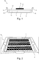
- Figure 1 and Figure 2 show a packaging unit 10 for a metal ceramic substrate 1.
- the packaging unit 10 comprises a first shell 4, a second shell 4 '(in Figure 4 ) and a substrate 1.
- the substrate 1 can be produced by a direct copper bonding (DCB) process or direct aluminum bonding (DAB) process and can comprise a large number of individual substrates arranged next to one another ( Figure 2 ).
- the substrate 1 is placed in the first shell 4 and the second shell 4 '(in Figure 4 ) is placed on the first shell 4, so that an underside of the substrate 1 is surrounded by the first shell 4 and an opposite upper side of the substrate 1 is covered by the second shell 4 '.
- DCB direct copper bonding
- DAB direct aluminum bonding
- the substrate 1 comprises a ceramic layer 11 and at least one metallization layer 12.
- the substrate 1 preferably has a total of two metallization layers, namely the metallization layer 12 and a further metallization layer, not shown, on the other side of the ceramic layer 11.
- a metal depot 2 is applied to an upper side of the metallization layer 12 of the substrate 1 and an adhesive point 3 is arranged on the metal depot 2.
- the metal depot 2 comprises a solderable or sinterable metal or a solderable or sinterable alloy.
- the adhesive point 3 is sticky and smearable at room temperature or in air.
- An electronic component for example a chip, illuminant, resistor, capacitor, etc., can be applied to the adhesive point 3.
- the first and the second shell 4, 4 ' can be constructed identically and can be made of plastic or cardboard.
- the first and the second shell 4, 4 ' comprise a bottom 7 and a circumferential wall 6.
- the circumferential wall 6 extends from the bottom 7 to a wall height in which only a substrate 1 plus a safety distance is enclosed.
- the peripheral wall 6 has a smaller outer dimension in the direction of the base 7 than at its free end.
- the first shell 4 and / or the second shell 4 ′ has at least one spacer 5 for support on the respective other shell and / or on the substrate 1.
- the fixing element can, for example, be an extended spacer or be set up separately at the level of the ceramic layer 11 or metallization layer 12.
- the packaging unit 10 can further have a further substrate 1 ', which is placed on the second shell 4'.
- a packaging stack can be realized which comprises a multiplicity of packaging units 10 stacked on top of one another and can be stored and / or transported in a space-saving manner without touching the adhesive points of the substrates.
- the packaging stack can further comprise a stabilizing element (not shown) which forms the end of the packaging stack.
Landscapes
- Engineering & Computer Science (AREA)
- Microelectronics & Electronic Packaging (AREA)
- Packaging Frangible Articles (AREA)
- Structures For Mounting Electric Components On Printed Circuit Boards (AREA)
Abstract
Description
- Die vorliegende Erfindung betrifft eine Verpackungseinheit für ein Substrat, einen Verpackungsstapel mit solchen Verpackungseinheiten und ein Verfahren zur Verpackung eines Substrats.
- Keramikschaltungsträger sind aufgrund ihrer hohen Wärmeleitfähigkeit, hohen Formstabilität bzw. mechanischen Festigkeit sowie ihrer hohen Isolationsfestigkeit insbesondere im Bereich der Hochleistungselektronik von Interesse.
-
DE 10 2010 018 668 B4 offenbart eine Verpackungseinheit aus einer Verpackung für Metall-Keramik-Substrate und mehreren Metall-Keramik-Substraten, jeweils bestehend aus einer Keramikschicht und aus auf wenigstens einer Oberflächenseite der Keramikschicht gebildeten Einzelmetallisierung und zwischen diesen verlaufenden Sollbruchlinien. -
DE 10 2012 106 087 B4 offenbart eine Verpackungseinheit für Substrate, insbesondere für Metall-Keramik-Substrate, bestehend aus einer Verpackung mit einem aus einem Flachmaterial hergestellten Verpackungsunterteil und einer von einer Vertiefung in einem oberen Bodenabschnitt des Verpackungsunterteils gebildeten Aufnahme für mehrere oder wenigstens einen Substratstapel oder Teilstapel. - Besonders für empfindliche Substrate und insbesondere Substrate mit empfindlichen Oberflächen oder Oberflächenabschnitten können diese Verpackungen aber noch verbessert werden.
- Es ist daher eine Aufgabe der vorliegenden Erfindung, eine Verpackungseinheit für Substrate bereitzustellen, mit welcher auch empfindliche Substrate sicher verpackt werden können.
- Diese Aufgabe wird durch eine Verpackungseinheit für ein Substrat, einen Verpackungsstapel mit einer Vielzahl solcher Verpackungseinheiten und ein Verfahren zur Verpackung eines Substrats nach den unabhängigen Ansprüchen gelöst. Vorteilhafte Ausführungsformen und Weiterbildungen sind den Unteransprüchen und der nachfolgenden Beschreibung zu entnehmen.
- Die Verpackungseinheit für ein Substrat umfasst eine erste Schale, ein Substrat und eine zweite Schale. Das Substrat ist in die erste Schale eingelegt und die zweite Schale ist auf die erste Schale aufgesetzt, sodass eine erste Seite des Substrats von der ersten Schale umgeben ist und eine gegenüberliegende, zweite Seite des Substrats von der zweiten Schale überdeckt wird. Auf die zweite Seite des Substrats ist ein Metalldepot aufgebracht und auf dem Metalldepot ist ein Klebepunkt angeordnet. Die zweite Schale stützt sich so an der ersten Schale ab, dass die zweite Schale das Substrat nur außerhalb des Klebepunkts berührt.
- Der Vorteil der erfindungsgemäßen Verpackungseinheit liegt darin, dass auch empfindliche Substrate sicher verpackt und insbesondere platzsparend gestapelt werden können, ohne den Klebepunkt auf dem Metalldepot zu berühren. Die erfindungsgemäße Verpackungseinheit ermöglicht, dass das Metalldepot und der Klebepunkt unmittelbar nach dem Herstellen des Substrates durch einen Hersteller oder Weiterverarbeiter des Substrats auf das Substrat aufgebracht werden können und das Substrat mit Metalldepot und Klebepunkt problemlos an einen Weiterverarbeiter oder einen Anwender verschickt werden kann. Auf diese Weise können Weiterverarbeiter oder Anwender des mit Metalldepot und Klebepunkt versehenen Substrats ein weiteres Bauteil direkt auf den Klebepunkt des Substrates aufbringen und beispielsweise mittels eines Löt- oder Sinterverfahrens das Bauteil direkt (ohne eine Vorarbeit zum Fixieren des Bauteils) befestigen. Dieses sogenannte Vorapplizieren des Metalldepots und des Klebepunkts ermöglicht, dass ein weiteres Bauteil kostengünstig auf dem Substrat befestigt werden kann. Bislang werden die Substrate generell ohne vorapplizierte Metall- oder Lotdepots hergestellt und vertrieben. Daher ist es nicht erforderlich, die Substrate anders als durch durchgängige Folien voneinander zu separieren. Im Falle eines Substrats mit vorappliziertem Metalldepot jedoch wird ein Klebepunkt auf das Substrat aufgebracht, der während des Verpackens und Versands der Teile nicht verschmiert oder berührt werden darf. Die erste und die zweite Schale können dazu beitragen, dass die Substrate platzsparend gestapelt, aufbewahrt und/oder transportiert werden können, ohne den Klebepunkt zu berühren.
- Das Substrat kann ein beliebiges Trägermaterial sein, welches zum Beispiel nicht sofort fertig verarbeitet wird und daher zunächst zuverlässig aufbewahrt werden muss. Das Substrat kann flächenförmig ausgebildet sein und eine flache ebene Struktur aufweisen. Beispielsweise kann das Substrat in der Halbleitertechnik ein Ausgangsmaterial für eine Fertigung von Elektronikmodulen sein. Das Substrat kann für eine elektronische Anwendung geeignet sein, bei der ein elektronisches Bauteil beispielsweise ein Chip, ein Schalter, ein Beleuchtungselement, ein Kondensator, ein Widerstand oder ähnliches auf das Substrat aufgebracht wird.
- Das Substrat weist auf seiner Oberfläche ein sogenanntes Metalldepot auf. Das Metalldepot, in anderen Worten ein Metallvorrat, kann je nach Einsatzzweck ein Metall oder mehrere verschiedene Metalle in bestimmten Mischungsverhältnissen umfassen oder daraus bestehen. Das Metalldepot kann beispielsweise für eine dauerhafte, feste Verbindung von Bauteilen geeignet sein, beispielsweise indem es sich als Schmelze mit der Oberfläche von Bauteilen verbindet bzw. legiert und nach Abkühlung erstarrt oder indem es sich im Sinne eines Sintermaterials ohne zu schmelzen mit der Oberfläche von Bauteilen verbindet. Größe und Dicke des Metalldepots können auch je nach Einsatzzweck variieren.
- Auf dem Metalldepot ist ein Klebepunkt angeordnet. Der Klebepunkt kann dazu dienen und dafür gestaltet sein, ein zum Beispiel elektronisches Bauteil auf dem Substrat zu fixieren, um einen darauffolgenden Löt- oder Sintervorgang zwischen dem elektronischen Bauteil und dem Substrat zu erleichtern. Der Klebepunkt kann beim Verlöten oder Sintern des elektronischen Bauteils mit dem Substrat unzersetzt verdampfen und/oder sich unter Zersetzung verflüchtigen, sodass der Klebepunkt keine oder keine störenden Rückstände hinterlässt.
- Das flächenförmige Substrat kann eine erste und zweite Seite aufweisen, die jeweils als Unter- und Oberseite bezeichnet werden können. Die "Unterseite" kann eine Oberfläche des Substrats sein, auf welcher weder Metalldepot noch Klebepunkt platziert ist. Im Gegensatz dazu kann eine "Oberseite" eine Oberfläche des Substrats sein, auf welcher das Metalldepot und der Klebepunkt appliziert sind.
- Die Verpackungseinheit weist eine erste und eine zweite Schale auf. Zumindest eine der ersten und zweiten Schalen kann wannenförmig ausgebildet sein, um das Substrat im Innenraum der Schale aufzunehmen. Auf diese Weise kann die erste Seite bzw. Unterseite des Substrats von der ersten Schale umgeben sein. Auf die erste Schale, in welche das Substrat eingelegt ist, kann die zweite Schale aufgesetzt werden. In anderen Worten können die erste und zweite Schale in vertikaler Richtung aufeinandergestapelt werden und das Substrat kann zwischen zwei aufeinanderfolgenden Schalen positioniert werden. Somit kann eine Bodenseite der zweiten Schale die zweite Seite bzw. Oberseite des Substrats überdecken.
- Die zweite Schale stützt sich so an der ersten Schale ab, dass die zweite Schale das Substrat nur außerhalb des Klebepunkts berührt. In anderen Worten, die zweite Schale berührt den Klebepunkt nicht, weder seitlich noch an der Oberseite des Klebepunkts. Auf diese Weise wird erreicht, dass der Klebepunkt nicht berührt bzw. verschmiert wird. Die zweite Schale kann auch so auf das erste Substrat aufgelegt sein, dass sie das erste Substrat auch nur außerhalb des Metalldepots berührt. Bevorzugt berührt die zweite Schale das Metalldepot weder seitlich noch an der Oberseite des Metalldepots. Auf diese Weise wird erreicht, dass auch das Metalldepot nicht berührt wird.
- In einer Ausführungsform ist das Substrat ein Metallkeramiksubstrat. In einer Ausführungsform umfasst das Metallkeramiksubstrat eine Keramikschicht und mindestens eine Metallisierungsschicht, wobei das Metalldepot auf die Metallisierungsschicht aufgebracht ist. In einer Ausführungsform umfasst das Metallkeramiksubstrat die Keramikschicht und zwei Metallisierungsschichten, wobei das Metalldepot auf eine der Metallisierungsschichten aufgebracht ist. In einer Ausführungsform umfasst das Metallkeramiksubstrat eine Keramikschicht und zwei Metallisierungsschichten und beide Metallisierungsschichten weisen eine außenliegende Oberfläche auf, auf die ein Metalldepot aufgebracht ist.
- Der Begriff "Metallkeramiksubstrat" kann so verstanden werden, dass das Substrat aus Keramik hergestellt und durch verschiedene Verfahren wie z.B. Direct-Copper-Bonding (üblicherweise als DCB-Verfahren bezeichnet), Direct-Aluminium-Bonding (üblicherweise als DAB-Verfahren bezeichnet) oder Active-Metal-Brazing (üblicherweise als AMB-Verfahren bezeichnet) metallisiert werden kann. Geeignete Materialien für das Keramiksubstrat sind beispielsweise ein Oxid, ein Nitrid, ein Carbid, oder ein Gemisch oder Komposit aus zumindest zweien dieser Materialien, insbesondere ggf. dotierte Aluminiumoxid- oder Siliziumnitrid-Keramik. Das nach der Metallisierung des Keramiksubstrats erhaltene Verbundmaterial wird auch als Metall-Keramik-Substrat oder Metall-Keramik-Verbund bezeichnet. Sofern es beispielsweise durch ein DCB-Verfahren hergestellt wurde, wird häufig auch die Bezeichnung "DCB-Substrat" verwendet.
- Eine Metallisierung des Keramiksubstrats kann beispielsweise dadurch realisiert werden, dass zunächst eine Metallfolie oxidiert wird, sodass sich an deren Oberfläche eine
- Metalloxidschicht bildet. Die oxidierte Metallfolie wird auf das Keramiksubstrat aufgelegt und das Keramiksubstrat mit der oxidierten Metallfolie erhitzt.
- Das Substrat kann ein Direct Copper Bonding (DCB) oder ein Direct Aluminium Bonding (DAB) Substrat sein, welches eine gute elektrische und thermische Verbindung elektronischer Bauteile und Chips über Kupfer bzw. Aluminium ermöglicht.
- Das Metalldepot kann im Falle eines lötbaren Metalls durch Löten, beispielsweise durch ein Vakuumlöten in einer aktiven Atmosphäre mit Ameisensäureaktivierung, auf das Metallkeramiksubstrat aufgebracht werden. Im Falle eines sinterbaren Metalls kann das Metalldepot durch Sintern oder Ansintern auf das Metallkeramiksubstrat aufgebracht werden. Das Metalldepot kann auf dem Metallkeramiksubstrat in einem definierten Volumen, an einer definierten Position und mit einer definierten Form appliziert werden. Auf diese Weise kann das Metallkeramiksubstrat ohne einen Metallpastendruck und/oder einen Reinigungsvorgang weiterverarbeitet werden. Dies ermöglicht, dass ein weiteres Bauteil, beispielsweise ein Chip, ein Schalter, ein Beleuchtungselement, ein Kondensator, ein Widerstand oder ähnliches auf das Substrat bzw. Metalldepot vereinfacht aufgebracht und dort beispielsweise ohne Verwendung von Hilfsstoffen wie beispielsweise Flussmitteln, Reinigungsmitteln und ähnlichem befestigt werden kann.
- In einer Ausführungsform umfasst das Metalldepot ein lötbares oder sinterbares Metall oder eine lötbare oder sinterbare Legierung. Das Metalldepot kann auch als ein Lot- oder Sinterdepot verstanden werden und ein bestimmtes Volumen aufweisen oder eine Metall-/Legierungsschicht sein. Das Metalldepot kann ein lötbares oder sinterbares Metall oder eine lötbare oder sinterbare Legierung sein.
- In einer Ausführungsform ist der Klebepunkt bei Raumtemperatur verschmierbar. Verschmierbar bedeutet, dass der Klebepunkt nach dem Applizieren auf den Metalldepots beispielsweise angetrocknet sein kann, jedoch an der Luft nicht fest oder hart wird, sondern klebrig oder schmierig bleibt. Der verschmierbare Klebepunkt ist weder vollständig fest noch vollständig flüssig. Er kann eine bestimmte Viskosität aufweisen, sodass sich beispielsweise ein auf den Klebepunkt aufgebrachtes weiteres Bauteil selbst bei einer zum Beispiel 90° schrägen Lage des Substrats nicht selbstständig bewegt oder selbstständig rutschen kann.
- Das Substrat kann aber auch auf beiden Seiten jeweils ein Metalldepot und auch einen Klebepunkt umfassen. Das bedeutet, dass das Substrat sowohl auf seiner Oberseite als auch auf seiner Unterseite ein Metalldepot und auch einen Klebepunkt aufweisen kann. Die erste und die zweite Schale können so eingerichtet sein, dass der in vertikaler Richtung (senkrecht zur Substratfläche) nach oben gerichtete Klebepunkt nicht mit der äußeren Bodenseite der zweiten Schale und der in vertikaler Richtung nach unten gerichtete Klebepunkt nicht mit der inneren Bodenseite der ersten Schale in Berührung kommen.
- In einer Ausführungsform weist die erste Schale und/oder die zweite Schale mindestens einen Abstandshalter zum Abstützen an der jeweils anderen Schale und/oder an dem Substrat auf. Der Abstandshalter kann beispielsweise an zumindest einer Wand der ersten und/oder der zweiten Schale ausgebildet sein, um sich an der jeweils anderen Schale abzustützen. Alternativ kann sich die äußere Bodenseite der zweiten Schale an dem Abstandshalter der ersten Schale abstützen. Der Abstandshalter kann beispielsweise punktförmig, stegförmig, kegelförmig oder ähnlich geformt sein oder entlang der Wand der ersten und/oder der zweiten Schale verlaufen.
- In einer Ausführungsform umfasst die erste Schale einen Boden und eine umlaufende Wand und die umlaufende Wand erstreckt sich vom Boden bis in eine Wandhöhe, die zwischen der Höhe des Substrats und der doppelten Höhe des Substrats liegt. In anderen Worten, die Wandhöhe ist größer als die Höhe bzw. Dicke eines Substrats und kleiner als die Höhe bzw. Dicke von zwei Substraten. In anderen Worten kann die erste Schale so eingerichtet sein, dass sie nur ein Substrat und nicht zwei Substrate aufnehmen kann. Das kann bedeuten, dass die Wandhöhe so groß ist wie die Höhe bzw. Dicke des Substrats plus einem Sicherheitsabstand. Noch genauer, die Wand kann eine Höhe aufweisen, die mindestens eine Summe der Höhe von Substrat, Metalldepot, Klebepunkt und Sicherheitsabstand beträgt. Der Sicherheitsabstand kann zum Beispiel 50 µm betragen. Die Wand der ersten Schale kann eine Höhe zwischen 200 und 1000 µm aufweisen.
- Der Boden der ersten Schale kann beispielsweise eine rechteckige Form aufweisen, um ein Substrat aufzunehmen, welches im Wesentlichen rechteckig eingerichtet ist. Die umlaufende Wand der ersten Schale kann senkrecht zum Boden der Schale stehen oder sich allmählich vom Boden in Richtung eines freien Endes der Schale aufweiten. In einer Ausführungsform weist die umlaufende Wand in Richtung des Bodens eine geringere Außenabmessung als an ihrem freien Ende auf. In anderen Worten die umlaufende Wand der ersten Schale kann kegelförmig ausgebildet sein, sodass sich die Wand in Richtung des freien Endes der Schale aufweitet. Auf diese Weise kann die zweite Schale einfach von der ersten Schale getrennt werden.
- In einer Ausführungsform weist die erste Schale mindestens ein Fixierungselement zur seitlichen Fixierung des Substrats relativ zu der ersten Schale und/oder der zweiten Schale auf. Das Fixierungselement kann verhindern, dass sich das Substrat beim Transport bewegt bzw. seitlich zusammengedrückt wird. Das Fixierungselement kann gleichzeitig auch ein Abstandshalter zum Abstützen an der jeweils anderen Schale und/oder an dem Substrat sein. Das Fixierungselement kann punktförmig, stegförmig, kegelförmig oder ähnlich geformt sein.
- In einer Ausführungsform sind die erste Schale und die zweite Schale baugleich. Die erste und zweite Schale können aber auch beispielsweise je nach Größe und Position des Metalldepots und des Klebepunkts unterschiedlich ausgelegt sein.
- In einer Ausführungsform umfasst das Substrat eine Vielzahl von nebeneinander angeordneten Einzelsubstraten. Das Einzelsubstrat kann in Form eines oben beschriebenen Substrats vorliegen. Alternativ ist es auch möglich, dass das Substrat eine oder mehrere (bevorzugt geradlinig verlaufende) Sollbruchlinien aufweist, die das Substrat in zwei oder mehr Bereiche unterteilen.
- In einer Ausführungsform sind die erste Schale und die zweite Schale aus Kunststoff oder Karton. Auf diese Weise können die Schalen kostengünstig, leicht und einfach hergestellt werden. Die erste und die zweite Schale können aber auch aus unterschiedlichen Materialien hergestellt werden. Die Materialien können dabei durchsichtig ausgebildet sein.
- In einer Ausführungsform umfasst die Verpackungseinheit ein weiteres Substrat, welches in die zweite Schale eingelegt ist. Selbstverständlich kann die Verpackungseinheit eine Vielzahl von abwechselnd angeordneten Substraten und Schalen umfassen. Auf diese Weise können Substrate und Schalen platzsparend gestapelt werden. Eine Schale, welche am oberen Ende der Verpackungseinheiten aufgelegt wird, kann einen Abschluss der Verpackungseinheit bilden.
- Die vorliegende Erfindung umfasst weiterhin einen Verpackungsstapel, welcher eine Vielzahl von aufeinandergestapelten Verpackungseinheiten umfasst. Durch eine relativ flache Konfiguration des Substrats und der Schale kann es möglich sein, dass eine Vielzahl von Substraten und Schalen platzsparend aufeinandergestapelt werden. Die Abstandshalter der ersten und zweiten Schale können ermöglichen, dass die Klebepunkte auf den Metalldepots trotz des Stapelns von mehreren Substraten und Schalen berührungsfrei bleiben. Der Verpackungsstapel kann je nach Einsatzzweck und Lagerkapazität eine beliebige Anzahl von Verpackungseinheiten aufweisen.
- In einer Ausführungsform umfasst der Verpackungsstapel ein Stabilisierungselement, welches den Abschluss des Verpackungsstapels bildet. Das Stabilisierungselement kann beispielsweise eine weitere Schale sein, auf welche kein Substrat mehr aufgelegt wird. Alternativ kann das Stabilisierungselement auch ein Deckel oder eine Folie sein, die den Abschluss des Verpackungsstapels bilden. Das Stabilisierungselement kann als eine Schutzabdeckung dienen und unter Vakuum stabil bleiben ohne sich zu biegen, wenn der Verpackungsstapel vakuumiert werden soll.
- Die vorliegende Erfindung umfasst weiterhin ein Verfahren zur Verpackung eines Substrats. Das Verfahren umfasst die folgenden Schritte:
- Bereitstellen einer ersten Schale,
- Einlegen eines Substrats in die erste Schale, und
- Aufsetzen einer zweiten Schale auf die erste Schale.
- Eine erste Seite des Substrats ist von der ersten Schale umgeben und eine gegenüberliegende, zweite Seite des Substrats wird von der zweiten Schale überdeckt, wobei auf die zweite Seite des Substrats ein Metalldepot aufgebracht ist und auf dem Metalldepot ein Klebepunkt angeordnet ist. Die zweite Schale stützt sich so an der ersten Schale ab, dass die zweite Schale das Substrat nur außerhalb des Klebepunkts berührt.
- Weitere Merkmale, Vorteile und Anwendungsmöglichkeiten der vorliegenden Erfindung ergeben sich aus der nachfolgenden Beschreibung, den Ausführungsbeispielen und den Figuren. Alle beschriebenen und/oder bildlich dargestellten Merkmale können unabhängig von ihrer Darstellung in einzelnen Ansprüchen, Figuren, Sätzen oder Absätzen miteinander kombiniert werden. In den Figuren stehen gleiche Bezugszeichen für gleiche oder ähnliche Objekte.
-
-
Figur 1 zeigt eine Verpackungseinheit gemäß einer Ausführungsform. -
Figur 2 zeigt eine Verpackungseinheit gemäß einer Ausführungsform. -
Figur 3 zeigt ein Metallkeramiksubstrat gemäß einer Ausführungsform. -
Figur 4 zeigt einen Verpackungsstapel gemäß einer Ausführungsform. -
Figur 1 und Figur 2 zeigen eine Verpackungseinheit 10 für ein Metallkeramiksubstrat 1. Die Verpackungseinheit 10 umfasst eine erste Schale 4, eine zweite Schale 4' (inFigur 4 ) und ein Substrat 1. Das Substrat 1 kann durch ein Direct Copper Bonding (DCB) Verfahren oder Direct Aluminium Bonding (DAB) Verfahren hergestellt werden und eine Vielzahl von nebeneinander angeordneten Einzelsubstraten umfassen (Figur 2 ). Das Substrat 1 ist in die erste Schale 4 eingelegt und die zweite Schale 4' (inFigur 4 ) ist auf die erste Schale 4 aufgesetzt, so dass eine Unterseite des Substrats 1 von der ersten Schale 4 umgeben ist und eine gegenüberliegende Oberseite des Substrats 1 von der zweiten Schale 4' überdeckt wird. - Das Substrat 1 umfasst eine Keramikschicht 11 und mindestens eine Metallisierungsschicht 12. Das Substrat 1 weist vorzugsweise insgesamt zwei Metallisierungsschichten auf, nämlich die Metallisierungsschicht 12 und eine nicht gezeigte weitere Metallisierungsschicht auf der anderen Seite der Keramikschicht 11. Wie auch in
Figur 3 gezeigt, ist auf eine Oberseite der Metallisierungsschicht 12 des Substrats 1 ein Metalldepot 2 aufgebracht und auf dem Metalldepot 2 ist ein Klebepunkt 3 angeordnet. Das Metalldepot 2 umfasst ein lötbares oder sinterbares Metall oder eine lötbare oder sinterbare Legierung. Der Klebepunkt 3 ist bei Raumtemperatur bzw. in Luft klebrig und verschmierbar. Auf dem Klebepunkt 3 kann ein elektronisches Bauteil beispielsweise ein Chip, Leuchtmittel, Widerstand, Kondensator etc. aufgebracht werden. - Die erste und die zweite Schale 4, 4' können baugleich ausgebildet sein und aus Kunststoff oder Karton hergestellt sein. Die erste und die zweite Schale 4, 4' umfassen einen Boden 7 und eine umlaufende Wand 6. Die umlaufende Wand 6 erstreckt sich vom Boden 7 bis in eine Wandhöhe, in der nur ein Substrat 1 plus ein Sicherheitsabstand umschlossen wird. Die umlaufende Wand 6 weist in Richtung des Bodens 7 eine geringere Außenabmessung als an ihrem freien Ende auf. Die erste Schale 4 und/oder die zweite Schale 4' weist mindestens einen Abstandshalter 5 zum Abstützen an der jeweils anderen Schale und/oder an dem Substrat 1 auf. Ferner, die erste und die zweite Schale 4, 4' können ein Fixierungselement (nicht gezeigt) zur seitlichen Fixierung des Substrats 1 relativ zu der ersten Schale 4 und/oder zu der zweiten Schale 4' aufweisen. Das Fixierungselement kann beispielsweise ein verlängerter Abstandshalter sein oder separat auf der Höhe der Keramikschicht 11 oder Metallisierungsschicht 12 eingerichtet sein. Wenn die zweite Schale 4' auf die erste Schale 4 aufgesetzt wird, soll sich die zweite Schale 4' so an der ersten Schale 4 abstützen, dass die zweite Schale 4 das Substrat 1 nur außerhalb des Klebepunkts 3 berührt.
- Wie in
Figur 4 gezeigt, kann die Verpackungseinheit 10 weiterhin ein weiteres Substrat 1' aufweisen, welches auf die zweite Schale 4' aufgelegt wird. Auf diese Weise kann ein Verpackungsstapel realisiert werden, welcher eine Vielzahl von aufeinandergestapelten Verpackungseinheiten 10 umfasst und platzsparend aufbewahren und/oder transportieren kann, ohne die Klebepunkte der Substrate zu berühren. Der Verpackungsstapel kann ferner ein Stabilisierungselement (nicht gezeigt) umfassen, welches den Abschluss des Verpackungsstapels bildet. - Ergänzend sei darauf hingewiesen, dass "umfassend" und "aufweisend" keine anderen Elemente oder Schritte ausschließt und "eine" oder "ein" keine Vielzahl ausschließt. Ferner sei darauf hingewiesen, dass Merkmale oder Schritte, die mit Verweis auf eines der obigen Ausführungsbeispiele beschrieben worden sind, auch in Kombination mit anderen Merkmalen oder Schritten anderer oben beschriebener Ausführungsbeispiele verwendet werden können. Bezugszeichen in den Ansprüchen sind nicht als Einschränkungen anzusehen.
Claims (15)
- Eine Verpackungseinheit (10) für ein Substrat (1), umfassend:- eine erste Schale (4),- ein Substrat (1), und- eine zweite Schale (4'),wobei das Substrat (1) in die erste Schale (4) eingelegt ist und die zweite Schale (4') auf die erste Schale (4) aufgesetzt ist, sodass eine erste Seite des Substrats (1) von der ersten Schale (4) umgeben ist und eine gegenüberliegende, zweite Seite des Substrats (1) von der zweiten Schale (4') überdeckt wird,
wobei auf die zweite Seite des Substrats (1) ein Metalldepot (2) aufgebracht ist und auf dem Metalldepot (2) ein Klebepunkt (3) angeordnet ist, und
wobei sich die zweite Schale (4') so an der ersten Schale (4) abstützt, dass die zweite Schale (4') das Substrat (1) nur außerhalb des Klebepunkts (3) berührt. - Verpackungseinheit nach Anspruch 1, wobei das Substrat (1) ein Metallkeramiksubstrat ist.
- Verpackungseinheit nach dem vorherigen Anspruch, wobei das Metallkeramiksubstrat (1) eine Keramikschicht (11) und mindestens eine Metallisierungsschicht (12) umfasst und das Metalldepot (2) auf die Metallisierungsschicht (12) aufgebracht ist.
- Verpackungseinheit nach einem der vorherigen Ansprüche, wobei das Metalldepot (2) ein lötbares oder sinterbares Metall oder eine lötbare oder sinterbare Legierung umfasst.
- Verpackungseinheit nach einem der vorherigen Ansprüche, wobei die erste Schale (4) und/oder die zweite Schale (4') mindestens einen Abstandshalter (5) zum Abstützen an der jeweils anderen Schale und/oder an dem Substrat (1) aufweist.
- Verpackungseinheit nach einem der vorherigen Ansprüche, wobei die erste Schale (4) einen Boden (7) und eine umlaufende Wand (6) umfasst, und
wobei sich die umlaufende Wand (6) vom Boden (7) bis in eine Wandhöhe erstreckt, die zwischen der Höhe des Substrats (1) und der doppelten Höhe des Substrats (1) liegt. - Verpackungseinheit nach dem vorherigen Anspruch, wobei die umlaufende Wand (6) in Richtung des Bodens (7) eine geringere Außenabmessung aufweist als an ihrem freien Ende.
- Verpackungseinheit nach einem der vorherigen Ansprüche, wobei die erste Schale (4) und die zweite Schale (4') baugleich sind.
- Verpackungseinheit nach einem der vorherigen Ansprüche, wobei der Klebepunkt (3) gestaltet ist, um ein elektronisches Bauteil auf dem Substrat (1) zu fixieren.
- Verpackungseinheit nach einem der vorherigen Ansprüche, wobei das Substrat (1) eine Vielzahl von nebeneinander angeordneten Einzelsubstraten umfasst.
- Verpackungseinheit nach einem der vorherigen Ansprüche, wobei die erste Schale (4) und die zweite Schale (4') aus Kunststoff oder Karton sind.
- Verpackungseinheit nach einem der vorherigen Ansprüche, weiterhin umfassend ein weiteres Substrat (1'), welches in die zweite Schale (4') eingelegt ist.
- Ein Verpackungsstapel, umfassend eine Vielzahl von aufeinandergestapelten Verpackungseinheiten nach einem der vorherigen Ansprüche.
- Verpackungsstapel nach dem vorherigen Anspruch, weiterhin umfassend ein Stabilisierungselement, welches den Abschluss des Verpackungsstapels bildet.
- Ein Verfahren zur Verpackung eines Substrats (1), umfassend die folgenden Schritte:- Bereitstellen einer ersten Schale (4),- Einlegen eines Substrats (1) in die erste Schale (4), und- Aufsetzen einer zweiten Schale (4') auf die erste Schale (4),
sodass eine erste Seite des Substrats (1) von der ersten Schale (4) umgeben ist und eine gegenüberliegende, zweite Seite des Substrats (1) von der zweiten Schale (4') überdeckt wird,
wobei auf die zweite Seite des Substrats (1) ein Metalldepot (2) aufgebracht ist und auf dem Metalldepot (2) ein Klebepunkt (3) angeordnet ist, und
wobei sich die zweite Schale (4') so an der ersten Schale (4) abstützt, dass die zweite Schale (4') das Substrat (1) nur außerhalb des Klebepunkts (3) berührt.
Priority Applications (3)
| Application Number | Priority Date | Filing Date | Title |
|---|---|---|---|
| EP18210738.3A EP3664129B1 (de) | 2018-12-06 | 2018-12-06 | Verpackungseinheit für ein substrat |
| US17/309,556 US20220022336A1 (en) | 2018-12-06 | 2019-11-21 | Packaging unit for a substrate |
| PCT/EP2019/082030 WO2020114791A1 (de) | 2018-12-06 | 2019-11-21 | Verpackungseinheit für ein substrat |
Applications Claiming Priority (1)
| Application Number | Priority Date | Filing Date | Title |
|---|---|---|---|
| EP18210738.3A EP3664129B1 (de) | 2018-12-06 | 2018-12-06 | Verpackungseinheit für ein substrat |
Publications (2)
| Publication Number | Publication Date |
|---|---|
| EP3664129A1 true EP3664129A1 (de) | 2020-06-10 |
| EP3664129B1 EP3664129B1 (de) | 2022-02-02 |
Family
ID=64661082
Family Applications (1)
| Application Number | Title | Priority Date | Filing Date |
|---|---|---|---|
| EP18210738.3A Active EP3664129B1 (de) | 2018-12-06 | 2018-12-06 | Verpackungseinheit für ein substrat |
Country Status (3)
| Country | Link |
|---|---|
| US (1) | US20220022336A1 (de) |
| EP (1) | EP3664129B1 (de) |
| WO (1) | WO2020114791A1 (de) |
Citations (8)
| Publication number | Priority date | Publication date | Assignee | Title |
|---|---|---|---|---|
| US6296122B1 (en) * | 1997-11-14 | 2001-10-02 | Sharp Kabushiki Kaisha | Packaging tray |
| JP2005132438A (ja) * | 2003-10-30 | 2005-05-26 | Kyocera Corp | 電子部品収納用トレイ |
| JP2011016557A (ja) * | 2009-07-09 | 2011-01-27 | Sekisui Plastics Co Ltd | 部品包装用トレイ |
| JP2011148510A (ja) * | 2010-01-19 | 2011-08-04 | Toshiba Logistics Corp | 収納トレイ |
| DE102010018668B4 (de) | 2010-04-07 | 2012-11-15 | Curamik Electronics Gmbh | Verpackungseinheit für Metall-Keramik-Substrate |
| WO2013047338A1 (ja) * | 2011-09-27 | 2013-04-04 | シャープ株式会社 | 物品包装構造 |
| DE102012106087B4 (de) | 2011-07-29 | 2015-10-22 | Rogers Germany Gmbh | Verpackungseinheit für Substrate |
| CN106742537B (zh) * | 2017-03-08 | 2018-09-28 | 武汉华星光电技术有限公司 | 一种用于盛放液晶显示面板的托盘 |
Family Cites Families (1)
| Publication number | Priority date | Publication date | Assignee | Title |
|---|---|---|---|---|
| US6049972A (en) * | 1997-03-04 | 2000-04-18 | Tessera, Inc. | Universal unit strip/carrier frame assembly and methods |
-
2018
- 2018-12-06 EP EP18210738.3A patent/EP3664129B1/de active Active
-
2019
- 2019-11-21 US US17/309,556 patent/US20220022336A1/en not_active Abandoned
- 2019-11-21 WO PCT/EP2019/082030 patent/WO2020114791A1/de not_active Ceased
Patent Citations (8)
| Publication number | Priority date | Publication date | Assignee | Title |
|---|---|---|---|---|
| US6296122B1 (en) * | 1997-11-14 | 2001-10-02 | Sharp Kabushiki Kaisha | Packaging tray |
| JP2005132438A (ja) * | 2003-10-30 | 2005-05-26 | Kyocera Corp | 電子部品収納用トレイ |
| JP2011016557A (ja) * | 2009-07-09 | 2011-01-27 | Sekisui Plastics Co Ltd | 部品包装用トレイ |
| JP2011148510A (ja) * | 2010-01-19 | 2011-08-04 | Toshiba Logistics Corp | 収納トレイ |
| DE102010018668B4 (de) | 2010-04-07 | 2012-11-15 | Curamik Electronics Gmbh | Verpackungseinheit für Metall-Keramik-Substrate |
| DE102012106087B4 (de) | 2011-07-29 | 2015-10-22 | Rogers Germany Gmbh | Verpackungseinheit für Substrate |
| WO2013047338A1 (ja) * | 2011-09-27 | 2013-04-04 | シャープ株式会社 | 物品包装構造 |
| CN106742537B (zh) * | 2017-03-08 | 2018-09-28 | 武汉华星光电技术有限公司 | 一种用于盛放液晶显示面板的托盘 |
Also Published As
| Publication number | Publication date |
|---|---|
| US20220022336A1 (en) | 2022-01-20 |
| EP3664129B1 (de) | 2022-02-02 |
| WO2020114791A1 (de) | 2020-06-11 |
Similar Documents
| Publication | Publication Date | Title |
|---|---|---|
| DE68908808T2 (de) | Verfahren zum Montieren elektronischer Mikrokomponenten auf einer Unterlage und Zwischenprodukt. | |
| DE102021131621B4 (de) | Verbindungsmaterial zum verbinden sich überlappender komponenten von leistungselektronischen geräten | |
| DE102012106087A1 (de) | Verpackung für Substrate sowie Verpackungseinheit mit einer solchen Verpackung | |
| EP3664129B1 (de) | Verpackungseinheit für ein substrat | |
| EP3958302A1 (de) | Bodenplatte für ein halbleitermodul und verfahren zum herstellen einer bodenplatte | |
| EP3664128B1 (de) | Verpackungseinheit für substrate | |
| EP3664130B1 (de) | Verpackungseinheit für ein substrat | |
| EP0006444A1 (de) | Vielschichtiges, dielektrisches Substrat | |
| DE102017206930A1 (de) | Lotformteil zum Diffusionslöten, Verfahren zu dessen Herstellung und Verfahren zu dessen Montage | |
| DE112020004962T5 (de) | Leiterplatte und verfahren zur herstellung einer leiterplatte | |
| DE19758452C2 (de) | Verfahren zum Herstellen eines Metall-Keramik-Substrates und Metall-Keramik-Substrat | |
| DE102016200062B4 (de) | Verfahren zur Ausbildung elektrisch leitender Durchkontaktierungen in keramischen Schaltungsträgern | |
| DE3323830C2 (de) | Anordnung zum Auflöten einer elektrischen Schaltungsplatte auf einen Grundkörper | |
| DE102019105465B3 (de) | Drucksintervorrichtung und Verfahren zum Herstellen eines elektronischen Bauteils | |
| EP2936950B1 (de) | Verfahren zur herstellung eines mehrschichtträgerkörpers | |
| DE102020107311B4 (de) | Verfahren zur Feinstrukturierung von metallhaltigen Schichten und keramisches Vielschichtbauteil | |
| DE102019106394A1 (de) | Verfahren zum Herstellen einer kohäsiven Verbindung | |
| DE102006012232B4 (de) | Verfahren zur selektiven Herstellung von Folienlaminaten zum Packaging und zur Isolation von ungehäusten elektronischen Bauelementen und Leiterbahnen | |
| DE102023127156A1 (de) | Verfahren zur Herstellung einer Halbleitervorrichtung und Halbleitervorrichtung | |
| DE1285581C2 (de) | Traeger mit einer Mikroschaltung und Verfahren zu seiner Herstellung | |
| DE7628700U1 (de) | Elektronische Baugruppe | |
| EP3644348A1 (de) | Verfahren zur herstellung eines substrats | |
| EP4443487A1 (de) | Substratanordnung mit oberflächenstruktur | |
| EP4443488A1 (de) | Substratanordnung mit oberflächenstruktur | |
| DD151529A1 (de) | Keramischer kondensator und verfahren zu dessen herstellung |
Legal Events
| Date | Code | Title | Description |
|---|---|---|---|
| PUAI | Public reference made under article 153(3) epc to a published international application that has entered the european phase |
Free format text: ORIGINAL CODE: 0009012 |
|
| STAA | Information on the status of an ep patent application or granted ep patent |
Free format text: STATUS: REQUEST FOR EXAMINATION WAS MADE |
|
| 17P | Request for examination filed |
Effective date: 20181206 |
|
| AK | Designated contracting states |
Kind code of ref document: A1 Designated state(s): AL AT BE BG CH CY CZ DE DK EE ES FI FR GB GR HR HU IE IS IT LI LT LU LV MC MK MT NL NO PL PT RO RS SE SI SK SM TR |
|
| AX | Request for extension of the european patent |
Extension state: BA ME |
|
| GRAP | Despatch of communication of intention to grant a patent |
Free format text: ORIGINAL CODE: EPIDOSNIGR1 |
|
| STAA | Information on the status of an ep patent application or granted ep patent |
Free format text: STATUS: GRANT OF PATENT IS INTENDED |
|
| INTG | Intention to grant announced |
Effective date: 20210907 |
|
| GRAS | Grant fee paid |
Free format text: ORIGINAL CODE: EPIDOSNIGR3 |
|
| GRAA | (expected) grant |
Free format text: ORIGINAL CODE: 0009210 |
|
| STAA | Information on the status of an ep patent application or granted ep patent |
Free format text: STATUS: THE PATENT HAS BEEN GRANTED |
|
| AK | Designated contracting states |
Kind code of ref document: B1 Designated state(s): AL AT BE BG CH CY CZ DE DK EE ES FI FR GB GR HR HU IE IS IT LI LT LU LV MC MK MT NL NO PL PT RO RS SE SI SK SM TR |
|
| REG | Reference to a national code |
Ref country code: GB Ref legal event code: FG4D Free format text: NOT ENGLISH |
|
| REG | Reference to a national code |
Ref country code: CH Ref legal event code: EP Ref country code: AT Ref legal event code: REF Ref document number: 1466807 Country of ref document: AT Kind code of ref document: T Effective date: 20220215 |
|
| REG | Reference to a national code |
Ref country code: DE Ref legal event code: R096 Ref document number: 502018008690 Country of ref document: DE |
|
| REG | Reference to a national code |
Ref country code: IE Ref legal event code: FG4D Free format text: LANGUAGE OF EP DOCUMENT: GERMAN |
|
| REG | Reference to a national code |
Ref country code: LT Ref legal event code: MG9D |
|
| REG | Reference to a national code |
Ref country code: NL Ref legal event code: MP Effective date: 20220202 |
|
| PG25 | Lapsed in a contracting state [announced via postgrant information from national office to epo] |
Ref country code: SE Free format text: LAPSE BECAUSE OF FAILURE TO SUBMIT A TRANSLATION OF THE DESCRIPTION OR TO PAY THE FEE WITHIN THE PRESCRIBED TIME-LIMIT Effective date: 20220202 Ref country code: RS Free format text: LAPSE BECAUSE OF FAILURE TO SUBMIT A TRANSLATION OF THE DESCRIPTION OR TO PAY THE FEE WITHIN THE PRESCRIBED TIME-LIMIT Effective date: 20220202 Ref country code: PT Free format text: LAPSE BECAUSE OF FAILURE TO SUBMIT A TRANSLATION OF THE DESCRIPTION OR TO PAY THE FEE WITHIN THE PRESCRIBED TIME-LIMIT Effective date: 20220602 Ref country code: NO Free format text: LAPSE BECAUSE OF FAILURE TO SUBMIT A TRANSLATION OF THE DESCRIPTION OR TO PAY THE FEE WITHIN THE PRESCRIBED TIME-LIMIT Effective date: 20220502 Ref country code: NL Free format text: LAPSE BECAUSE OF FAILURE TO SUBMIT A TRANSLATION OF THE DESCRIPTION OR TO PAY THE FEE WITHIN THE PRESCRIBED TIME-LIMIT Effective date: 20220202 Ref country code: LT Free format text: LAPSE BECAUSE OF FAILURE TO SUBMIT A TRANSLATION OF THE DESCRIPTION OR TO PAY THE FEE WITHIN THE PRESCRIBED TIME-LIMIT Effective date: 20220202 Ref country code: HR Free format text: LAPSE BECAUSE OF FAILURE TO SUBMIT A TRANSLATION OF THE DESCRIPTION OR TO PAY THE FEE WITHIN THE PRESCRIBED TIME-LIMIT Effective date: 20220202 Ref country code: ES Free format text: LAPSE BECAUSE OF FAILURE TO SUBMIT A TRANSLATION OF THE DESCRIPTION OR TO PAY THE FEE WITHIN THE PRESCRIBED TIME-LIMIT Effective date: 20220202 Ref country code: BG Free format text: LAPSE BECAUSE OF FAILURE TO SUBMIT A TRANSLATION OF THE DESCRIPTION OR TO PAY THE FEE WITHIN THE PRESCRIBED TIME-LIMIT Effective date: 20220502 |
|
| PG25 | Lapsed in a contracting state [announced via postgrant information from national office to epo] |
Ref country code: PL Free format text: LAPSE BECAUSE OF FAILURE TO SUBMIT A TRANSLATION OF THE DESCRIPTION OR TO PAY THE FEE WITHIN THE PRESCRIBED TIME-LIMIT Effective date: 20220202 Ref country code: LV Free format text: LAPSE BECAUSE OF FAILURE TO SUBMIT A TRANSLATION OF THE DESCRIPTION OR TO PAY THE FEE WITHIN THE PRESCRIBED TIME-LIMIT Effective date: 20220202 Ref country code: GR Free format text: LAPSE BECAUSE OF FAILURE TO SUBMIT A TRANSLATION OF THE DESCRIPTION OR TO PAY THE FEE WITHIN THE PRESCRIBED TIME-LIMIT Effective date: 20220503 Ref country code: FI Free format text: LAPSE BECAUSE OF FAILURE TO SUBMIT A TRANSLATION OF THE DESCRIPTION OR TO PAY THE FEE WITHIN THE PRESCRIBED TIME-LIMIT Effective date: 20220202 |
|
| PG25 | Lapsed in a contracting state [announced via postgrant information from national office to epo] |
Ref country code: IS Free format text: LAPSE BECAUSE OF FAILURE TO SUBMIT A TRANSLATION OF THE DESCRIPTION OR TO PAY THE FEE WITHIN THE PRESCRIBED TIME-LIMIT Effective date: 20220602 |
|
| PG25 | Lapsed in a contracting state [announced via postgrant information from national office to epo] |
Ref country code: SM Free format text: LAPSE BECAUSE OF FAILURE TO SUBMIT A TRANSLATION OF THE DESCRIPTION OR TO PAY THE FEE WITHIN THE PRESCRIBED TIME-LIMIT Effective date: 20220202 Ref country code: SK Free format text: LAPSE BECAUSE OF FAILURE TO SUBMIT A TRANSLATION OF THE DESCRIPTION OR TO PAY THE FEE WITHIN THE PRESCRIBED TIME-LIMIT Effective date: 20220202 Ref country code: RO Free format text: LAPSE BECAUSE OF FAILURE TO SUBMIT A TRANSLATION OF THE DESCRIPTION OR TO PAY THE FEE WITHIN THE PRESCRIBED TIME-LIMIT Effective date: 20220202 Ref country code: EE Free format text: LAPSE BECAUSE OF FAILURE TO SUBMIT A TRANSLATION OF THE DESCRIPTION OR TO PAY THE FEE WITHIN THE PRESCRIBED TIME-LIMIT Effective date: 20220202 Ref country code: DK Free format text: LAPSE BECAUSE OF FAILURE TO SUBMIT A TRANSLATION OF THE DESCRIPTION OR TO PAY THE FEE WITHIN THE PRESCRIBED TIME-LIMIT Effective date: 20220202 Ref country code: CZ Free format text: LAPSE BECAUSE OF FAILURE TO SUBMIT A TRANSLATION OF THE DESCRIPTION OR TO PAY THE FEE WITHIN THE PRESCRIBED TIME-LIMIT Effective date: 20220202 |
|
| REG | Reference to a national code |
Ref country code: DE Ref legal event code: R097 Ref document number: 502018008690 Country of ref document: DE |
|
| PG25 | Lapsed in a contracting state [announced via postgrant information from national office to epo] |
Ref country code: AL Free format text: LAPSE BECAUSE OF FAILURE TO SUBMIT A TRANSLATION OF THE DESCRIPTION OR TO PAY THE FEE WITHIN THE PRESCRIBED TIME-LIMIT Effective date: 20220202 |
|
| PLBE | No opposition filed within time limit |
Free format text: ORIGINAL CODE: 0009261 |
|
| STAA | Information on the status of an ep patent application or granted ep patent |
Free format text: STATUS: NO OPPOSITION FILED WITHIN TIME LIMIT |
|
| 26N | No opposition filed |
Effective date: 20221103 |
|
| PG25 | Lapsed in a contracting state [announced via postgrant information from national office to epo] |
Ref country code: SI Free format text: LAPSE BECAUSE OF FAILURE TO SUBMIT A TRANSLATION OF THE DESCRIPTION OR TO PAY THE FEE WITHIN THE PRESCRIBED TIME-LIMIT Effective date: 20220202 |
|
| P01 | Opt-out of the competence of the unified patent court (upc) registered |
Effective date: 20230527 |
|
| PG25 | Lapsed in a contracting state [announced via postgrant information from national office to epo] |
Ref country code: IT Free format text: LAPSE BECAUSE OF FAILURE TO SUBMIT A TRANSLATION OF THE DESCRIPTION OR TO PAY THE FEE WITHIN THE PRESCRIBED TIME-LIMIT Effective date: 20220202 |
|
| GBPC | Gb: european patent ceased through non-payment of renewal fee |
Effective date: 20221206 |
|
| REG | Reference to a national code |
Ref country code: BE Ref legal event code: MM Effective date: 20221231 |
|
| PG25 | Lapsed in a contracting state [announced via postgrant information from national office to epo] |
Ref country code: LU Free format text: LAPSE BECAUSE OF NON-PAYMENT OF DUE FEES Effective date: 20221206 |
|
| PG25 | Lapsed in a contracting state [announced via postgrant information from national office to epo] |
Ref country code: IE Free format text: LAPSE BECAUSE OF NON-PAYMENT OF DUE FEES Effective date: 20221206 Ref country code: GB Free format text: LAPSE BECAUSE OF NON-PAYMENT OF DUE FEES Effective date: 20221206 |
|
| PG25 | Lapsed in a contracting state [announced via postgrant information from national office to epo] |
Ref country code: BE Free format text: LAPSE BECAUSE OF NON-PAYMENT OF DUE FEES Effective date: 20221231 |
|
| PGFP | Annual fee paid to national office [announced via postgrant information from national office to epo] |
Ref country code: FR Payment date: 20231222 Year of fee payment: 6 Ref country code: DE Payment date: 20231214 Year of fee payment: 6 |
|
| PG25 | Lapsed in a contracting state [announced via postgrant information from national office to epo] |
Ref country code: HU Free format text: LAPSE BECAUSE OF FAILURE TO SUBMIT A TRANSLATION OF THE DESCRIPTION OR TO PAY THE FEE WITHIN THE PRESCRIBED TIME-LIMIT; INVALID AB INITIO Effective date: 20181206 |
|
| PG25 | Lapsed in a contracting state [announced via postgrant information from national office to epo] |
Ref country code: CY Free format text: LAPSE BECAUSE OF FAILURE TO SUBMIT A TRANSLATION OF THE DESCRIPTION OR TO PAY THE FEE WITHIN THE PRESCRIBED TIME-LIMIT Effective date: 20220202 |
|
| PGFP | Annual fee paid to national office [announced via postgrant information from national office to epo] |
Ref country code: CH Payment date: 20240102 Year of fee payment: 6 |
|
| PG25 | Lapsed in a contracting state [announced via postgrant information from national office to epo] |
Ref country code: MK Free format text: LAPSE BECAUSE OF FAILURE TO SUBMIT A TRANSLATION OF THE DESCRIPTION OR TO PAY THE FEE WITHIN THE PRESCRIBED TIME-LIMIT Effective date: 20220202 |
|
| PG25 | Lapsed in a contracting state [announced via postgrant information from national office to epo] |
Ref country code: MC Free format text: LAPSE BECAUSE OF FAILURE TO SUBMIT A TRANSLATION OF THE DESCRIPTION OR TO PAY THE FEE WITHIN THE PRESCRIBED TIME-LIMIT Effective date: 20220202 |
|
| PG25 | Lapsed in a contracting state [announced via postgrant information from national office to epo] |
Ref country code: MC Free format text: LAPSE BECAUSE OF FAILURE TO SUBMIT A TRANSLATION OF THE DESCRIPTION OR TO PAY THE FEE WITHIN THE PRESCRIBED TIME-LIMIT Effective date: 20220202 |
|
| PG25 | Lapsed in a contracting state [announced via postgrant information from national office to epo] |
Ref country code: MT Free format text: LAPSE BECAUSE OF FAILURE TO SUBMIT A TRANSLATION OF THE DESCRIPTION OR TO PAY THE FEE WITHIN THE PRESCRIBED TIME-LIMIT Effective date: 20220202 |
|
| REG | Reference to a national code |
Ref country code: AT Ref legal event code: MM01 Ref document number: 1466807 Country of ref document: AT Kind code of ref document: T Effective date: 20231206 |
|
| PG25 | Lapsed in a contracting state [announced via postgrant information from national office to epo] |
Ref country code: AT Free format text: LAPSE BECAUSE OF NON-PAYMENT OF DUE FEES Effective date: 20231206 |
|
| REG | Reference to a national code |
Ref country code: DE Ref legal event code: R119 Ref document number: 502018008690 Country of ref document: DE |
|
| REG | Reference to a national code |
Ref country code: CH Ref legal event code: PL |
|
| PG25 | Lapsed in a contracting state [announced via postgrant information from national office to epo] |
Ref country code: DE Free format text: LAPSE BECAUSE OF NON-PAYMENT OF DUE FEES Effective date: 20250701 |
|
| PG25 | Lapsed in a contracting state [announced via postgrant information from national office to epo] |
Ref country code: FR Free format text: LAPSE BECAUSE OF NON-PAYMENT OF DUE FEES Effective date: 20241231 |
|
| PG25 | Lapsed in a contracting state [announced via postgrant information from national office to epo] |
Ref country code: CH Free format text: LAPSE BECAUSE OF NON-PAYMENT OF DUE FEES Effective date: 20241231 |
|
| PG25 | Lapsed in a contracting state [announced via postgrant information from national office to epo] |
Ref country code: TR Free format text: LAPSE BECAUSE OF FAILURE TO SUBMIT A TRANSLATION OF THE DESCRIPTION OR TO PAY THE FEE WITHIN THE PRESCRIBED TIME-LIMIT Effective date: 20220202 |
|
| PGFP | Annual fee paid to national office [announced via postgrant information from national office to epo] |
Ref country code: AT Payment date: 20260410 Year of fee payment: 5 |