EP3657674A1 - Electronic component housing package, electronic device, and electronic module - Google Patents
Electronic component housing package, electronic device, and electronic module Download PDFInfo
- Publication number
- EP3657674A1 EP3657674A1 EP18836129.9A EP18836129A EP3657674A1 EP 3657674 A1 EP3657674 A1 EP 3657674A1 EP 18836129 A EP18836129 A EP 18836129A EP 3657674 A1 EP3657674 A1 EP 3657674A1
- Authority
- EP
- European Patent Office
- Prior art keywords
- electronic component
- conductors
- connection conductors
- housing package
- base section
- Prior art date
- Legal status (The legal status is an assumption and is not a legal conclusion. Google has not performed a legal analysis and makes no representation as to the accuracy of the status listed.)
- Pending
Links
Images


Classifications
-
- H—ELECTRICITY
- H10—SEMICONDUCTOR DEVICES; ELECTRIC SOLID-STATE DEVICES NOT OTHERWISE PROVIDED FOR
- H10N—ELECTRIC SOLID-STATE DEVICES NOT OTHERWISE PROVIDED FOR
- H10N30/00—Piezoelectric or electrostrictive devices
- H10N30/80—Constructional details
- H10N30/88—Mounts; Supports; Enclosures; Casings
- H10N30/883—Additional insulation means preventing electrical, physical or chemical damage, e.g. protective coatings
-
- H—ELECTRICITY
- H03—ELECTRONIC CIRCUITRY
- H03H—IMPEDANCE NETWORKS, e.g. RESONANT CIRCUITS; RESONATORS
- H03H9/00—Networks comprising electromechanical or electro-acoustic elements; Electromechanical resonators
- H03H9/02—Details
- H03H9/05—Holders or supports
- H03H9/0504—Holders or supports for bulk acoustic wave devices
- H03H9/0514—Holders or supports for bulk acoustic wave devices consisting of mounting pads or bumps
- H03H9/0519—Holders or supports for bulk acoustic wave devices consisting of mounting pads or bumps for cantilever
-
- H—ELECTRICITY
- H03—ELECTRONIC CIRCUITRY
- H03H—IMPEDANCE NETWORKS, e.g. RESONANT CIRCUITS; RESONATORS
- H03H9/00—Networks comprising electromechanical or electro-acoustic elements; Electromechanical resonators
- H03H9/02—Details
- H03H9/02007—Details of bulk acoustic wave devices
- H03H9/02086—Means for compensation or elimination of undesirable effects
- H03H9/02094—Means for compensation or elimination of undesirable effects of adherence
-
- H—ELECTRICITY
- H03—ELECTRONIC CIRCUITRY
- H03H—IMPEDANCE NETWORKS, e.g. RESONANT CIRCUITS; RESONATORS
- H03H9/00—Networks comprising electromechanical or electro-acoustic elements; Electromechanical resonators
- H03H9/02—Details
- H03H9/02007—Details of bulk acoustic wave devices
- H03H9/02086—Means for compensation or elimination of undesirable effects
- H03H9/02133—Means for compensation or elimination of undesirable effects of stress
-
- H—ELECTRICITY
- H03—ELECTRONIC CIRCUITRY
- H03H—IMPEDANCE NETWORKS, e.g. RESONANT CIRCUITS; RESONATORS
- H03H9/00—Networks comprising electromechanical or electro-acoustic elements; Electromechanical resonators
- H03H9/02—Details
- H03H9/05—Holders or supports
- H03H9/10—Mounting in enclosures
- H03H9/1007—Mounting in enclosures for bulk acoustic wave [BAW] devices
- H03H9/1014—Mounting in enclosures for bulk acoustic wave [BAW] devices the enclosure being defined by a frame built on a substrate and a cap, the frame having no mechanical contact with the BAW device
- H03H9/1021—Mounting in enclosures for bulk acoustic wave [BAW] devices the enclosure being defined by a frame built on a substrate and a cap, the frame having no mechanical contact with the BAW device the BAW device being of the cantilever type
-
- H—ELECTRICITY
- H10—SEMICONDUCTOR DEVICES; ELECTRIC SOLID-STATE DEVICES NOT OTHERWISE PROVIDED FOR
- H10N—ELECTRIC SOLID-STATE DEVICES NOT OTHERWISE PROVIDED FOR
- H10N30/00—Piezoelectric or electrostrictive devices
- H10N30/80—Constructional details
- H10N30/87—Electrodes or interconnections, e.g. leads or terminals
- H10N30/875—Further connection or lead arrangements, e.g. flexible wiring boards, terminal pins
-
- H—ELECTRICITY
- H10—SEMICONDUCTOR DEVICES; ELECTRIC SOLID-STATE DEVICES NOT OTHERWISE PROVIDED FOR
- H10W—GENERIC PACKAGES, INTERCONNECTIONS, CONNECTORS OR OTHER CONSTRUCTIONAL DETAILS OF DEVICES COVERED BY CLASS H10
- H10W70/00—Package substrates; Interposers; Redistribution layers [RDL]
- H10W70/01—Manufacture or treatment
- H10W70/05—Manufacture or treatment of insulating or insulated package substrates, or of interposers, or of redistribution layers
- H10W70/098—Applying pastes or inks, e.g. screen printing
-
- H—ELECTRICITY
- H03—ELECTRONIC CIRCUITRY
- H03H—IMPEDANCE NETWORKS, e.g. RESONANT CIRCUITS; RESONATORS
- H03H9/00—Networks comprising electromechanical or electro-acoustic elements; Electromechanical resonators
- H03H9/02—Details
- H03H9/02535—Details of surface acoustic wave devices
- H03H9/02543—Characteristics of substrate, e.g. cutting angles
- H03H9/02582—Characteristics of substrate, e.g. cutting angles of diamond substrates
-
- H—ELECTRICITY
- H05—ELECTRIC TECHNIQUES NOT OTHERWISE PROVIDED FOR
- H05K—PRINTED CIRCUITS; CASINGS OR CONSTRUCTIONAL DETAILS OF ELECTRIC APPARATUS; MANUFACTURE OF ASSEMBLAGES OF ELECTRICAL COMPONENTS
- H05K1/00—Printed circuits
- H05K1/18—Printed circuits structurally associated with non-printed electric components
- H05K1/181—Printed circuits structurally associated with non-printed electric components associated with surface mounted components
-
- H—ELECTRICITY
- H05—ELECTRIC TECHNIQUES NOT OTHERWISE PROVIDED FOR
- H05K—PRINTED CIRCUITS; CASINGS OR CONSTRUCTIONAL DETAILS OF ELECTRIC APPARATUS; MANUFACTURE OF ASSEMBLAGES OF ELECTRICAL COMPONENTS
- H05K2201/00—Indexing scheme relating to printed circuits covered by H05K1/00
- H05K2201/10—Details of components or other objects attached to or integrated in a printed circuit board
- H05K2201/10007—Types of components
- H05K2201/10083—Electromechanical or electro-acoustic component, e.g. microphone
Definitions
- the present invention relates to an electronic component housing package that houses an electronic component such as a piezoelectric vibrator or a semiconductor element, an electronic device, and an electronic module.
- an electronic component housing package for mounting an electronic component such as a piezoelectric vibrator or a semiconductor element.
- a portion that houses an electronic component on an insulating substrate formed of, for example, a ceramic sintered body is closed by a lid body and airtightly sealed.
- Such an electronic component housing package basically includes, for example, an insulating substrate, a metalized layer, and wiring conductor.
- the insulating substrate includes a lower insulating layer and an upper insulating layer.
- the lower insulating layer has a flat-plate shape and includes a mounting section for electronic component on an upper surface thereof.
- the upper insulating layer has a frame shape and is superposed on the lower insulating layer so as to surround the mounting section.
- the metalized layer has a frame shape and serves as a surface for joining to a lid body.
- the metalized layer is formed on an upper surface of the insulating substrate.
- the wiring conductor is formed in a region from the mounting section to, for example, a lower surface of the lower insulating layer.
- connection conductors on which the electronic component is to be mounted are disposed on an upper surface of a step portion in some cases (for example, see Japanese Unexamined Patent Application Publication No. 2013-207527 ).
- An electronic component housing package includes a base section that includes a mounting section for an electronic component, a projecting part that is positioned on the base section and projects from the base section, a frame part that is positioned on the base section and surrounds the mounting section, a frame-shaped metalized layer that is positioned on the frame part, a plurality of external connection conductors that is positioned opposite the mounting section in a thickness direction, a connection conductor which is positioned on the projecting part and for connecting to the electronic component, and a wiring conductor that is connected to the connection conductor and that is led out to the base section, wherein a thickness of the connection conductor gradually increases from a side opposite the wiring conductor toward the wiring conductor.
- An electronic device includes the above-described electronic component housing package and the electronic component that is mounted in the electronic component housing package.
- An electronic module includes the above-described electronic device and a module substrate to which the electronic device is connected.
- Fig. 1 illustrates an example of an embodiment of the electronic component housing package according to the present disclosure seeing through an upper surface of the electronic component housing package.
- Fig. 2 is a longitudinal sectional view of the electronic component housing package taken along line X-X' illustrated in Fig. 1 .
- an insulating substrate 101 includes a frame part 106 and a base section 107.
- the frame part 106 and the base section 107 are superposed on each other.
- cutout portions 109 are disposed at side surfaces of the insulating substrate 101.
- Side conductors are disposed in the cutout portions 109.
- An electronic component housing package 100 includes the base section 107 and the frame part 106.
- the base section 107 includes a first main surface 102, a mounting section 105 for an electronic component 110, and a third main surface 104 disposed opposite the first main surface 102 on a side for attachment to a module substrate 130.
- the frame part 106 includes a second main surface 103 and is disposed on a sealing side.
- the electronic component 110 such as a piezoelectric vibrator is to be mounted on the mounting section 105.
- a wiring substrate (electronic component housing package 100) of the present example also includes a frame-shaped metalized layer 113 on an upper surface of the frame part 106, connection conductors 111 that is positioned in the base section 107 and for connecting to the electronic component 110, and wiring conductors 116 extending from the connection conductors 111.
- a lid body 115 is joined to an upper portion of the insulating substrate 101 by using a sealing material such as silver solder (not illustrated), thereby the electronic component 110 is airtightly sealed.
- the insulating substrate 101 is partially recessed in section in the thickness direction.
- An electronic device 120 is formed by airtightly sealing the electronic component 110 such as a piezoelectric vibrator in the electronic component housing package 100.
- the lid body 115 that seals the mounting section 105 is transparent in Fig. 1 for ease of seeing.
- the frame part 106 is superposed on the flat-plate shaped base section 107.
- the frame part 106 surrounds the mounting section 105 on the upper surface of the base section 107.
- Side surfaces of the frame part 106 and the base section 107 exposed in the frame part 106 form a recessed shape in which the mounting section 105 for mounting the electronic component 110 is provided.
- the frame part 106 and the base section 107 are formed of a ceramic material such as, for example, an aluminum oxide sintered body, an aluminum nitride sintered body, a mullite sintered body, or a glass-ceramic sintered body.
- the external shape of the entirety of the insulating substrate 101 is, for example, a rectangular shape in plan view having the sides the length of which is about 1.2 to 10 mm.
- the entirety of the insulating substrate 101 has a plate shape having a thickness of about 0.2 to 2 mm.
- the upper surface of the insulating substrate 101 has the recessed shape formed by the frame part 106 and the base section 107.
- the insulating substrate 101 is fabricated as follows: an appropriate organic binder, an appropriate solvent, an appropriate plasticizer, and the like are added to and mixed with material particles of aluminum oxide, silicon oxide, magnesium oxide, calcium oxide, and the like to obtain a slurry; this slurry is subjected to a sheet forming method such as, for example, a doctor blade method or a roll calendar method to be formed into a sheet shape.
- a plurality of ceramic green sheets is obtained; next, a subset of the ceramic green sheets is formed to have a frame shape by being subjected to an appropriate punching process; The ceramic green sheets are superposed in the up-down direction such that the frame-shaped ceramic green sheets are respectively positioned on upper surfaces of the flat plate-shaped ceramic green sheets not having been formed into the frame shape and then fired at high temperature.
- the insulating substrate 101 is fabricated by producing a matrix substrate in which substrate regions that respectively become individual insulating substrates 101 are arrayed and dividing the produced matrix substrate into the individual substrate regions.
- the matrix substrate includes a flat plate-shaped insulating layer including a plurality of regions that become base sections 107 and an insulating layer including a plurality of regions that respectively become frame parts 106 (a plurality of openings is arrayed). These insulating layers are superposed one on top of the other.
- the frame part 106 includes the frame-shaped metalized layer 113 at the upper surface thereof and may have the cutout portions 109 at outer side surfaces thereof.
- the base section 107 includes the connection conductors 111, the wiring conductors 116, the side conductors, and the external connection conductors 108 serving as conductor paths through which the electronic component 110 to be mounted on the mounting section 105 and an external electric circuit in the module substrate 130 are electrically connected to one another.
- the cutout portions 109 are disposed at corner portions of the insulating substrate 101 in the example herein, the cutout portions 109 may be disposed at the long sides or the short sides being other positions of the outer side surfaces of the insulating substrate 101 than the corner portions.
- the side conductors may be changed to through conductors or the like to obtain the insulating substrate 101 without the cutout portions 109.
- the frame part 106 may include two of more insulating layers so that the frame part 106 has stepped inner side surfaces for mounting the plurality of electronic components.
- TCXO temperature compensated crystal oscillator
- the mounting section 105 has a quadrangular shape in plan view to follow the quadrangular electronic component 110.
- a bottom portion of the recessed portion of the insulating substrate 101 has a quadrangular shape.
- a pair of connection conductors 111 is disposed at two corner portions adjacent to each other at the bottom portion of the recessed portion.
- the connection conductors 111 function as a conductor layer to which electrodes of the electronic component 110 such as a piezoelectric vibrator to be mounted on the mounting section 105 are connected.
- the external shape is typically a quadrangular shape in plan view, and a pair of electrodes (not illustrated) for connection is disposed at the corner portions.
- the connection conductors 111 are disposed at the corner portions of the bottom portion of the recessed portion.
- the electrodes of the electronic component 110 and the connection conductors 111 are connected to one another by using a joining material 114 such as an electrically conductive adhesive. That is, as illustrated in Fig. 1 , the electronic component 110 is positioned in the mounting section 105 such that a pair of electrodes at corner portions of the main surface of the electronic component 110 faces the pair of connection conductors 111 in the mounting section 105, and the joining material 114 having adhered to the connection conductors 111 in advance is heated and cured. Thus, the electrodes of the electronic component 110 and the connection conductors 111 are connected to each other.
- a joining material 114 such as an electrically conductive adhesive
- connection electrodes are disposed at one end portion of the piezoelectric vibrator and no connection electrode is disposed at another end portion.
- connection conductors 111 are disposed on upper surfaces of projecting parts 112 so that the connection conductors 111 can be mounted with a gap for avoiding contact with the mounting section 105 due to vibration, shock, or the like.
- connection conductors 111 and the projecting parts 112 are disposed at the above-described positions.
- the positions and shapes of the connection conductors 111 and the projecting parts 112 may be changed in accordance with the disposition of the other electronic component or the like.
- Examples of such other electronic component may include, for example, a piezoelectric element such as a ceramic piezoelectric element or a surface acoustic wave element, a semiconductor element, a capacitative element, a resistance element, and so forth.
- the electronic component housing package 100 includes the base section 107, the projecting parts 112, the frame part 106, the frame-shaped metalized layer 113, the plurality of external connection conductors 108, the connection conductors 111, and the wiring conductors 116.
- the base section 107 includes a mounting section 105 for the electronic component 110.
- the projecting parts 112 are positioned on the base section 107 and project from the base sections 107.
- the frame part 106 is positioned on the base section 107 and surrounds the mounting section 105.
- the frame-shaped metalized layer 113 is positioned on the frame part 106.
- the plurality of external connection conductors 108 is positioned opposite the mounting section 105 in the thickness direction.
- connection conductors 111 are positioned on the projecting parts 112 and for connecting to the electronic component 110.
- the wiring conductors 116 are connected to the connection conductors 111 and led out to the base section 107.
- the thickness of the connection conductors 111 gradually increases from a side opposite the wiring conductors 116 toward the wiring conductors 116.
- the thickness of metallization paste that becomes the wiring conductors 116 is largest at regions around the projecting parts 112 where flowing of the metalizing paste is largest.
- spreading due to the flowing of the metallization paste can reduce the likelihood of the occurrences of breaks in wiring or reduction in conductive property. That is, even if the width of the connection conductors 111 on the projecting parts 112 is reduced due to size reduction of the electronic component housing package 100, the connection conductors 111 spread during formation of the projecting parts 112 in the pressure applying process. This can reduce the likelihood of the occurrences of breaks in wiring or reduction in conductive property.
- connection conductors 111 are positioned on the projecting parts 112 and which includes the wiring conductors 116 connected to the connection conductors 111 as described above, for example, a plurality of through holes that becomes the cutout portions 109 is formed, by punching, at four corners of each of the wiring substrate regions of each of the subset of the ceramic green sheets that become the base section 107.
- the metallization paste that becomes the wiring conductors 116 is applied to predetermined positions by a screen printing method, and metallization paste is superposed on end portions of metallization paste so that the metallization paste that becomes the connection conductors 111 is similarly applied to predetermined positions. In so doing, the metallization paste is applied so as to ensure that regions where the metallization paste is superposed have a large width.
- the surface of the ceramic green sheet that becomes the base section 107 on which the metallization paste that becomes the connection conductors 111 is applied is subjected to pressure by using a pressure applying tool having recessed portions so that the connection conductors 111 project to form the projecting parts 112.
- a pressure applying tool having recessed portions so that the connection conductors 111 project to form the projecting parts 112.
- the connection conductors 111 on which the electronic component 110 is to be mounted are exposed in the upper surfaces of the projecting parts 112.
- the wiring conductors 116 are led from peripheral portions of the connection conductors 111 toward the mounting section 105. If the ceramic green sheet is subjected to the pressure by using the pressure applying tool, the ceramic green sheet and the metallization paste flow in the recessed portions of the tool.
- connection conductors 111 gradually increases from the side opposite the wiring conductors 116 toward the wiring conductors 116.
- Such a structure spreads the metallization paste that becomes the wiring conductors 116 during the formation of the projecting parts 112 in the pressure applying process. This can reduce the likelihood of the occurrences of breaks in wiring or reduction in conductive property.
- the depth of the recessed portions of the pressure applying tool is uniform and the height of the projecting parts 112 after the pressure applying process can be uniform.
- dimensional accuracy of the thickness of the connection conductors 111 can be improved.
- the frame part 106 and the base section 107 are separately formed and, after the projecting parts 112 have been formed by the pressure applying process, superposed on each other to produce the matrix substrate.
- the metallization paste that becomes the connection conductors 111 and the ceramic paste that becomes the wiring conductors 116 may be applied to a single ceramic green sheet and the pressure may be applied to collectively form the projecting parts 112 and the frame part 106.
- dimensional accuracy of the shape of the projecting parts 112 including the connection conductors 111 in the mounting section 105 can be improved by using a pressure applying tool with high dimensional accuracy.
- a single ceramic green sheet to which metallization paste that becomes, for example, the external connection conductors 108 or the like is applied may be superposed on the side to be connected to the module substrate 130 so as to produce the matrix substrate.
- connection conductors 111 include inclined parts 117 inclined toward the wiring conductors 116.
- the connection conductors 111 on which the electronic component 110 is to be mounted are buried in the projecting parts 112 by using the inclined parts 117 in lower portions of the connection conductors 111.
- the electronic device 120 in which removal of the connection conductors 111 due to shocks from outside is suppressed and which exhibits good shock resistance can be realized.
- the pressure is applied, by using the pressure applying tool having recessed portions, to the surface of the ceramic green sheet that becomes the base section 107 on which the metallization paste that becomes the connection conductors 111 is applied, so that the connection conductors 111 project to form the projecting parts 112.
- the thickness of the connection conductors 111 and the wiring conductors 116 as conductors can be increased by using the inclined parts 117 at outer peripheries of the projecting parts 112, and the connection conductors 111 are buried in the projecting parts 112 by using the inclined parts 117 in the lower portions of the connection conductors 111. Accordingly, at outer peripheries of the connection conductors 111 on a side connected to the wiring conductors 116, even if the electronic component 110 is vibrated by shocks from outside and the outer peripheries of the connection conductors 111 are locally subjected to stress, removal of the connection conductors 111 from the projecting parts 112 is suppressed.
- connection conductors 111 are buried in the projecting parts 112 by using the inclined parts 117 in the lower portions of the connection conductors 111, removal of the connection conductors 111 from the projecting parts 112 is suppressed.
- the electronic device 120 in which connection between the electronic component 110 and the connection conductors 111 is good and which exhibits good shock resistance can be realized.
- the width of the end portions of the metallization paste gradually reduces toward distal ends and the width of the inclined parts 117 gradually reduces from the wiring conductor 116 side toward the side opposite the wiring conductors 116.
- the inclined parts 117 in which the thickness of the connection conductors 111 is more effectively buried in the projecting parts 112 can be provided in a region from the side opposite the wiring conductors 116 toward the wiring conductors 116. Since local concentration of the spreading of the metallization paste is reduced by the inclined parts 117, the likelihood of the occurrences of break in wiring or reduction in conductive property due to the spreading of the metallization paste that becomes the wiring conductors 116 can be effectively reduced in the formation of the projecting parts 112 by using the pressure applying process.
- the shape of the metallization paste for forming the connection conductors 111 on which the electronic component 110 is to be mounted do not change due to the pressure applying process.
- a type of metallization paste containing a large amount of a solid of metal particles can be used for suppressing the changes in shape in the pressure applying process.
- the metallization paste that forms the wiring conductors 116 led from the connection conductors 111 improve fluidity in the pressure applying process so as to suppress breaks in wiring. Accordingly, for improving the fluidity in the pressure applying process, for example, a type of the metallization paste containing a reduced amount of a solid of the metal particles and an increased amount of binder can be used.
- the electronic component housing package 100 which exhibits a good forming property of the projecting parts 112 in the pressure applying process and in which the shape of the connection conductors 111 is maintained and breaks in the wiring conductors 116 is suppressed in the pressure applying process can be fabricated.
- the wiring conductors 116 are covered with an insulating layer 118 except for portions thereof at the side surfaces of the projecting parts 112.
- connection conductors 111 to which the electronic component 110 is connected can be suppressed. That is, since high dimensional accuracy as the connection conductors 111 can be obtained and the wiring conductors 116 at the base section 107 are covered with the insulating layer 118, shorting with other surrounding wiring conductors such as, for example, other connection conductors or wiring conductors on the first main surface 102 of the mounting section 105 (not illustrated) can be suppressed. Furthermore, if the joining material 114 flows during, for example, joining of the electronic component 110, shorting with other wiring conductors can be suppressed and the electronic component housing package 100 in which the electronic component 110 exhibits good reliability in attachment can be realized.
- Fig. 4 illustrates an enlarged view of a main portion of the electronic component housing package 100 in which, as described above, the wiring conductors 116 are covered with the insulating layer 118 except for the portions thereof at the side surfaces of the projecting parts 112.
- the metallization paste that becomes the wiring conductors 116 is, in each of the wiring substrate regions of the ceramic green sheet, applied to predetermined positions by the screen printing method, and further, the metallization paste is superposed on the end portions of the metallization paste so that the metallization paste that becomes the connection conductors 111 is similarly applied to the predetermined positions.
- ceramic paste that becomes the insulating layer 118 is applied to a predetermined position by a screen printing method so as to cover the metallization paste that becomes the wiring conductors 116.
- the pressure can be applied, by using the pressure applying tool having recessed portions, so that the connection conductors 111 project from the base section 107 to form the projecting parts 112.
- the connection conductors 111 on which the electronic component 110 is to be mounted are exposed in the upper surfaces of the projecting parts 112.
- the wiring conductors 116 covered with the insulating layer 118 except for the portions thereof at the side surfaces of the projecting parts 112 are provided from the peripheral portions of the connection conductors 111.
- the reason for applying the ceramic paste that becomes the insulating layer 118 except for the portions that become the side surfaces of the projecting parts 112 is to suppress substantial reduction of the area to be connected to the electronic component 110 due to covering of part of the connection conductors 111 as a result of spreading of the metallization paste that becomes the wiring conductors 116 and the ceramic paste that becomes the insulating layer 118 if the projecting parts 112 are formed in the pressure applying process. It is desirable that the ceramic paste be formed by the substantially same material as that of the insulating substrate 101.
- the term "same material" refers to a material containing the same ceramic component as that of the insulating substrate 101 after firing. Amounts to add a binder and a solvent mixed with the ceramic are adjusted in accordance with specifications of a method of applying the ceramic paste (for example, the screen printing or the like).
- the matrix substrate may be produced by separately forming the frame part 106 and the base section 107 and superposing the frame part 106 and the base section 107 on each other after the projecting parts 112 have been formed in the pressure applying process. If the thickness of the frame part 106 is comparatively small, the metallization paste that becomes, for example, the connection conductors 111 and, for example, the ceramic paste that becomes the insulating layer 118 may be formed in a single ceramic green sheet and the pressure may be applied to collectively form recesses that become the projecting parts 112 and the frame part 106.
- the matrix substrate may be produced by superposing a single ceramic green sheet to which the metallization paste that becomes, for example, the external connection conductors 108 or the like is applied on the side to be connected to the module substrate 130.
- dimensional accuracy of the connection conductors 111 and dimensional accuracy of the shape of the projecting parts 112 including the connection conductors 111 can be improved by using the pressure applying tool with high dimensional accuracy.
- the electronic device 120 includes the electronic component housing package 100 of any one of the above descriptions and the electronic component 110 mounted in the electronic component housing package 100.
- the connection conductors 111 on which the electronic component 110 is mounted are buried in the projecting parts 112 by using the inclined parts 117 in lower portions of the connection conductors 111.
- removal of the connection conductors 111 due to shocks from outside is suppressed and good shock resistance is obtained.
- the thickness of the connection conductors 111 and the wiring conductors 116 as conductors can be increased by using the inclined parts 117 at the outer peripheries of the projecting parts 112, and the connection conductors 111 are buried in the projecting parts 112 by using the inclined parts 117 in the lower portions of the connection conductors 111.
- the area for joining to the projecting parts 112 that is the total of rear surfaces of the connection conductors 111 and rear surfaces of the inclined parts 117 is large.
- the connection conductors 111 and the inclined parts 117 can be disposed at the projecting parts 112.
- the electronic device 120 in which removal of the connection conductors 111 due to shocks from outside is suppressed and which exhibits good shock resistance can be realized.
- the wiring conductors 116 are covered with the insulating layer 118 except for the portions thereof at the side surfaces of the projecting parts 112 in the electronic component housing package 100, connectivity between the electronic component 110 and the connection conductors 111 can be maintained in a good state and shorting with surrounding wiring conductors or the like can be suppressed. That is, even if the wiring conductors 116 are led from the outer peripheries of the projecting parts 112 to an outer periphery of the electronic component housing package 100, shorting with the surrounding wiring conductors or the like can be suppressed with the wiring conductors 116 covered with the insulating layer 118.
- An electronic module 140 includes the above-described electronic device 120 and the module substrate 130 to which the electronic device 120 is connected. With such a structure, the electronic module 140 exhibiting good reliability in operation can be provided.
- the electronic device 120 that is mounted in this electronic module 140 exhibits good electrical connectivity, through the wiring conductors 116 or the like, with the connection conductors 111 to which the electronic component 110 housed in the electronic component housing package 100 is connected.
- the electronic module 140 which exhibits good reliability in operation and in which the electronic device 120 is mounted can be provided.
- the connection conductors 111 and the inclined parts 117 are disposed in the projecting parts 112
- the electronic component 110 such as a piezoelectric vibrator is joined to the connection conductors 111 in the upper surfaces of the projecting parts 112 by using the joining material 114
- the inclined parts 117 in lower portions of the connection conductors 111 are buried in the projecting parts 112
- breaks or reduction in conductive property in the wiring conductors 116 led from the outer peripheries of the projecting parts 112 to the outer periphery of the electronic component housing package 100 is suppressed.
- connection conductors 111 to which the electronic component 110 is connected can be suppressed.
- connection conductors 111 are disposed in the projecting parts 112 with high dimensional accuracy, shorting with the surrounding wiring conductors or the like can be suppressed.
- the present disclosure is not limited to the above-described example according to the embodiment and can be changed in various manners without departing from the gist of the present disclosure.
- the projecting parts 112, the connection conductors 111, and the like form pairs and are disposed near the short side of the insulating substrate 101.
- the positions and the numbers of the projecting parts 112, the connection conductors 111, and the like may be changed in accordance with, for example, the type, the number of terminals, and the shape of the electronic component to be mounted on the mounting section 105.
- the cutout portions 109 are disposed at four corner portions of the electronic component housing package 100.
- the projecting parts 112, the connection conductors 111, and the like may be disposed at the long side or both the short and the long sides of the electronic component housing package 100 without the cutout portions 109 at the four corner portions of the electronic component housing package 100, and the electronic component may be connected onto these connection conductors 111.
Landscapes
- Physics & Mathematics (AREA)
- Acoustics & Sound (AREA)
- Piezo-Electric Or Mechanical Vibrators, Or Delay Or Filter Circuits (AREA)
Abstract
Description
- The present invention relates to an electronic component housing package that houses an electronic component such as a piezoelectric vibrator or a semiconductor element, an electronic device, and an electronic module.
- Nowadays, an electronic component housing package for mounting an electronic component such as a piezoelectric vibrator or a semiconductor element is used. Typically, in such an electronic component housing package, a portion that houses an electronic component on an insulating substrate formed of, for example, a ceramic sintered body is closed by a lid body and airtightly sealed. Such an electronic component housing package basically includes, for example, an insulating substrate, a metalized layer, and wiring conductor. The insulating substrate includes a lower insulating layer and an upper insulating layer. The lower insulating layer has a flat-plate shape and includes a mounting section for electronic component on an upper surface thereof. The upper insulating layer has a frame shape and is superposed on the lower insulating layer so as to surround the mounting section. The metalized layer has a frame shape and serves as a surface for joining to a lid body. The metalized layer is formed on an upper surface of the insulating substrate. The wiring conductor is formed in a region from the mounting section to, for example, a lower surface of the lower insulating layer. After the electronic component has been mounted on a plurality of connection conductors in the mounting section and electrodes of the electronic component have been electrically connected to the connection conductors, the lid body formed of metal is joined, with a brazing alloy or the like, to an upper surface of the frame-shaped metalized layer on a frame part, and the electronic component is airtightly sealed in a housing including the insulating substrate and the lid body. Thus, an electronic device is fabricated. If the electronic component is, for example, a piezoelectric vibrator, the connection conductors on which the electronic component is to be mounted are disposed on an upper surface of a step portion in some cases (for example, see Japanese Unexamined Patent Application Publication No.
2013-207527 - An electronic component housing package according to the present disclosure includes a base section that includes a mounting section for an electronic component, a projecting part that is positioned on the base section and projects from the base section, a frame part that is positioned on the base section and surrounds the mounting section, a frame-shaped metalized layer that is positioned on the frame part, a plurality of external connection conductors that is positioned opposite the mounting section in a thickness direction, a connection conductor which is positioned on the projecting part and for connecting to the electronic component, and a wiring conductor that is connected to the connection conductor and that is led out to the base section, wherein a thickness of the connection conductor gradually increases from a side opposite the wiring conductor toward the wiring conductor.
- An electronic device according to the present disclosure includes the above-described electronic component housing package and the electronic component that is mounted in the electronic component housing package.
- An electronic module according to the present disclosure includes the above-described electronic device and a module substrate to which the electronic device is connected.
-
-
Fig. 1 illustrates an electronic component housing package and so forth according to an embodiment seeing through the top of the electronic component housing package. -
Fig. 2 is a longitudinal sectional view of the electronic component housing package and so forth according to the present embodiment taken along line X-X' illustrated inFig. 1 . -
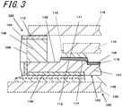
Fig. 3 is a longitudinal sectional view of a main portion illustrating the main portion of the electronic component housing package and so forth according to the present embodiment. -
Fig. 4 is a longitudinal sectional view of a main portion illustrating another example of the electronic component housing package and so forth according to the present embodiment. - An electronic component housing package and so forth according to the present disclosure is described with reference to the accompanying drawings.
Fig. 1 illustrates an example of an embodiment of the electronic component housing package according to the present disclosure seeing through an upper surface of the electronic component housing package.Fig. 2 is a longitudinal sectional view of the electronic component housing package taken along line X-X' illustrated inFig. 1 . - Referring to
Fig. 1 , aninsulating substrate 101 includes aframe part 106 and abase section 107. Theframe part 106 and thebase section 107 are superposed on each other. For example,cutout portions 109 are disposed at side surfaces of theinsulating substrate 101. Side conductors are disposed in thecutout portions 109. An electroniccomponent housing package 100 includes thebase section 107 and theframe part 106. Thebase section 107 includes a firstmain surface 102, amounting section 105 for anelectronic component 110, and a thirdmain surface 104 disposed opposite the firstmain surface 102 on a side for attachment to amodule substrate 130. Theframe part 106 includes a secondmain surface 103 and is disposed on a sealing side. Theelectronic component 110 such as a piezoelectric vibrator is to be mounted on themounting section 105. -
External connection conductors 108 connected to the side conductors are disposed on a lower surface side of theinsulating substrate 101. A wiring substrate (electronic component housing package 100) of the present example also includes a frame-shapedmetalized layer 113 on an upper surface of theframe part 106,connection conductors 111 that is positioned in thebase section 107 and for connecting to theelectronic component 110, andwiring conductors 116 extending from theconnection conductors 111. Regarding the electroniccomponent housing package 100, alid body 115 is joined to an upper portion of theinsulating substrate 101 by using a sealing material such as silver solder (not illustrated), thereby theelectronic component 110 is airtightly sealed. - According to the present embodiment, the
insulating substrate 101 is partially recessed in section in the thickness direction. Anelectronic device 120 is formed by airtightly sealing theelectronic component 110 such as a piezoelectric vibrator in the electroniccomponent housing package 100. Thelid body 115 that seals themounting section 105 is transparent inFig. 1 for ease of seeing. - In the
insulating substrate 101, theframe part 106 is superposed on the flat-plateshaped base section 107. In plan view, theframe part 106 surrounds themounting section 105 on the upper surface of thebase section 107. Side surfaces of theframe part 106 and thebase section 107 exposed in theframe part 106 form a recessed shape in which themounting section 105 for mounting theelectronic component 110 is provided. - The
frame part 106 and thebase section 107 are formed of a ceramic material such as, for example, an aluminum oxide sintered body, an aluminum nitride sintered body, a mullite sintered body, or a glass-ceramic sintered body. The external shape of the entirety of theinsulating substrate 101 is, for example, a rectangular shape in plan view having the sides the length of which is about 1.2 to 10 mm. The entirety of theinsulating substrate 101 has a plate shape having a thickness of about 0.2 to 2 mm. The upper surface of theinsulating substrate 101 has the recessed shape formed by theframe part 106 and thebase section 107. If theframe part 106 and thebase section 107 are formed of an aluminum oxide sintered body, theinsulating substrate 101 is fabricated as follows: an appropriate organic binder, an appropriate solvent, an appropriate plasticizer, and the like are added to and mixed with material particles of aluminum oxide, silicon oxide, magnesium oxide, calcium oxide, and the like to obtain a slurry; this slurry is subjected to a sheet forming method such as, for example, a doctor blade method or a roll calendar method to be formed into a sheet shape. Thus, a plurality of ceramic green sheets is obtained; next, a subset of the ceramic green sheets is formed to have a frame shape by being subjected to an appropriate punching process; The ceramic green sheets are superposed in the up-down direction such that the frame-shaped ceramic green sheets are respectively positioned on upper surfaces of the flat plate-shaped ceramic green sheets not having been formed into the frame shape and then fired at high temperature. - For example, the
insulating substrate 101 is fabricated by producing a matrix substrate in which substrate regions that respectively become individualinsulating substrates 101 are arrayed and dividing the produced matrix substrate into the individual substrate regions. The matrix substrate includes a flat plate-shaped insulating layer including a plurality of regions that becomebase sections 107 and an insulating layer including a plurality of regions that respectively become frame parts 106 (a plurality of openings is arrayed). These insulating layers are superposed one on top of the other. - The
frame part 106 includes the frame-shapedmetalized layer 113 at the upper surface thereof and may have thecutout portions 109 at outer side surfaces thereof. Thebase section 107 includes theconnection conductors 111, thewiring conductors 116, the side conductors, and theexternal connection conductors 108 serving as conductor paths through which theelectronic component 110 to be mounted on themounting section 105 and an external electric circuit in themodule substrate 130 are electrically connected to one another. Although thecutout portions 109 are disposed at corner portions of theinsulating substrate 101 in the example herein, thecutout portions 109 may be disposed at the long sides or the short sides being other positions of the outer side surfaces of theinsulating substrate 101 than the corner portions. The side conductors may be changed to through conductors or the like to obtain theinsulating substrate 101 without thecutout portions 109. - If a plurality of electronic components such as a temperature compensated crystal oscillator (TCXO) and so forth (not illustrated) are to be mounted on the
mounting section 105 of the electronic device, theframe part 106 may include two of more insulating layers so that theframe part 106 has stepped inner side surfaces for mounting the plurality of electronic components. - For example, the
mounting section 105 has a quadrangular shape in plan view to follow the quadrangularelectronic component 110. Likewise, a bottom portion of the recessed portion of theinsulating substrate 101 has a quadrangular shape. In the example illustrated inFig. 1 , a pair ofconnection conductors 111 is disposed at two corner portions adjacent to each other at the bottom portion of the recessed portion. Theconnection conductors 111 function as a conductor layer to which electrodes of theelectronic component 110 such as a piezoelectric vibrator to be mounted on themounting section 105 are connected. If theelectronic component 110 is a piezoelectric vibrator, the external shape is typically a quadrangular shape in plan view, and a pair of electrodes (not illustrated) for connection is disposed at the corner portions. In order to connect such electrodes easily and reliably, theconnection conductors 111 are disposed at the corner portions of the bottom portion of the recessed portion. - The electrodes of the
electronic component 110 and theconnection conductors 111 are connected to one another by using a joiningmaterial 114 such as an electrically conductive adhesive. That is, as illustrated inFig. 1 , theelectronic component 110 is positioned in the mountingsection 105 such that a pair of electrodes at corner portions of the main surface of theelectronic component 110 faces the pair ofconnection conductors 111 in the mountingsection 105, and the joiningmaterial 114 having adhered to theconnection conductors 111 in advance is heated and cured. Thus, the electrodes of theelectronic component 110 and theconnection conductors 111 are connected to each other. If theelectronic component 110 to be mounted is a piezoelectric vibrator, connection electrodes are disposed at one end portion of the piezoelectric vibrator and no connection electrode is disposed at another end portion. Thus, theconnection conductors 111 are disposed on upper surfaces of projectingparts 112 so that theconnection conductors 111 can be mounted with a gap for avoiding contact with the mountingsection 105 due to vibration, shock, or the like. - In the example according to the present embodiment, as the example in which the piezoelectric vibrator is used as the
electronic component 110, theconnection conductors 111 and the projectingparts 112 are disposed at the above-described positions. However, if mounting another electronic component or a plurality of other electronic components, the positions and shapes of theconnection conductors 111 and the projectingparts 112 may be changed in accordance with the disposition of the other electronic component or the like. Examples of such other electronic component may include, for example, a piezoelectric element such as a ceramic piezoelectric element or a surface acoustic wave element, a semiconductor element, a capacitative element, a resistance element, and so forth. - The electronic
component housing package 100 according to the present disclosure includes thebase section 107, the projectingparts 112, theframe part 106, the frame-shapedmetalized layer 113, the plurality ofexternal connection conductors 108, theconnection conductors 111, and thewiring conductors 116. Thebase section 107 includes a mountingsection 105 for theelectronic component 110. The projectingparts 112 are positioned on thebase section 107 and project from thebase sections 107. Theframe part 106 is positioned on thebase section 107 and surrounds the mountingsection 105. The frame-shapedmetalized layer 113 is positioned on theframe part 106. The plurality ofexternal connection conductors 108 is positioned opposite the mountingsection 105 in the thickness direction. Theconnection conductors 111 are positioned on the projectingparts 112 and for connecting to theelectronic component 110. The wiringconductors 116 are connected to theconnection conductors 111 and led out to thebase section 107. The thickness of theconnection conductors 111 gradually increases from a side opposite thewiring conductors 116 toward the wiringconductors 116. - With the above-described structure, in a pressure applying process for fabricating the superposed structure that becomes the matrix substrate including wiring substrate regions that become electronic
component housing packages 100, the thickness of metallization paste that becomes the wiringconductors 116 is largest at regions around the projectingparts 112 where flowing of the metalizing paste is largest. Thus, spreading due to the flowing of the metallization paste can reduce the likelihood of the occurrences of breaks in wiring or reduction in conductive property. That is, even if the width of theconnection conductors 111 on the projectingparts 112 is reduced due to size reduction of the electroniccomponent housing package 100, theconnection conductors 111 spread during formation of the projectingparts 112 in the pressure applying process. This can reduce the likelihood of the occurrences of breaks in wiring or reduction in conductive property. - Hereinafter, an example of fabrication of the electronic
component housing package 100 according to the present disclosure is specifically described. In order to fabricate the electroniccomponent housing package 100 in which theconnection conductors 111 are positioned on the projectingparts 112 and which includes the wiringconductors 116 connected to theconnection conductors 111 as described above, for example, a plurality of through holes that becomes thecutout portions 109 is formed, by punching, at four corners of each of the wiring substrate regions of each of the subset of the ceramic green sheets that become thebase section 107. In each of the wiring substrate regions of the ceramic green sheet, the metallization paste that becomes the wiringconductors 116 is applied to predetermined positions by a screen printing method, and metallization paste is superposed on end portions of metallization paste so that the metallization paste that becomes theconnection conductors 111 is similarly applied to predetermined positions. In so doing, the metallization paste is applied so as to ensure that regions where the metallization paste is superposed have a large width. - Next, the surface of the ceramic green sheet that becomes the
base section 107 on which the metallization paste that becomes theconnection conductors 111 is applied is subjected to pressure by using a pressure applying tool having recessed portions so that theconnection conductors 111 project to form the projectingparts 112. Thus, theconnection conductors 111 on which theelectronic component 110 is to be mounted are exposed in the upper surfaces of the projectingparts 112. In addition, the wiringconductors 116 are led from peripheral portions of theconnection conductors 111 toward the mountingsection 105. If the ceramic green sheet is subjected to the pressure by using the pressure applying tool, the ceramic green sheet and the metallization paste flow in the recessed portions of the tool. Thus, a structure in which the thickness of theconnection conductors 111 gradually increases from the side opposite thewiring conductors 116 toward the wiringconductors 116 can be obtained. Such a structure spreads the metallization paste that becomes the wiringconductors 116 during the formation of the projectingparts 112 in the pressure applying process. This can reduce the likelihood of the occurrences of breaks in wiring or reduction in conductive property. - The depth of the recessed portions of the pressure applying tool is uniform and the height of the projecting
parts 112 after the pressure applying process can be uniform. Thus, compared to a method in which printing with the metallization paste on the mountingsection 105 is performed a plurality of times so as to form metalized bumps to provide theconnection conductors 111 as is the case with the related art, dimensional accuracy of the thickness of theconnection conductors 111 can be improved. By superposing a corresponding one of the subset of the ceramic green sheets that becomes theframe part 106 on the ceramic green sheet on which the projectingparts 112 are disposed and which becomes thebase section 107, the matrix substrate in which a plurality of the wiring substrate regions that becomes the electroniccomponent housing packages 100 is arrayed can be produced. - In the above-described example, the
frame part 106 and thebase section 107 are separately formed and, after the projectingparts 112 have been formed by the pressure applying process, superposed on each other to produce the matrix substrate. However, if the thickness of theframe part 106 is comparatively small, the metallization paste that becomes theconnection conductors 111 and the ceramic paste that becomes the wiringconductors 116 may be applied to a single ceramic green sheet and the pressure may be applied to collectively form the projectingparts 112 and theframe part 106. With such a method, dimensional accuracy of the shape of the projectingparts 112 including theconnection conductors 111 in the mountingsection 105 can be improved by using a pressure applying tool with high dimensional accuracy. A single ceramic green sheet to which metallization paste that becomes, for example, theexternal connection conductors 108 or the like is applied may be superposed on the side to be connected to themodule substrate 130 so as to produce the matrix substrate. - In the electronic
component housing package 100 according to the present disclosure, theconnection conductors 111 includeinclined parts 117 inclined toward the wiringconductors 116. With such a structure, theconnection conductors 111 on which theelectronic component 110 is to be mounted are buried in the projectingparts 112 by using theinclined parts 117 in lower portions of theconnection conductors 111. Thus, theelectronic device 120 in which removal of theconnection conductors 111 due to shocks from outside is suppressed and which exhibits good shock resistance can be realized. - Specifically, in order to fabricate the electronic
component housing package 100 illustrated inFig. 3 in which theconnection conductors 111 are positioned on the projectingparts 112 and which includes the wiringconductors 116 connected to theconnection conductors 111 as described above, the pressure is applied, by using the pressure applying tool having recessed portions, to the surface of the ceramic green sheet that becomes thebase section 107 on which the metallization paste that becomes theconnection conductors 111 is applied, so that theconnection conductors 111 project to form the projectingparts 112. As a result, the thickness of theconnection conductors 111 and thewiring conductors 116 as conductors can be increased by using theinclined parts 117 at outer peripheries of the projectingparts 112, and theconnection conductors 111 are buried in the projectingparts 112 by using theinclined parts 117 in the lower portions of theconnection conductors 111. Accordingly, at outer peripheries of theconnection conductors 111 on a side connected to thewiring conductors 116, even if theelectronic component 110 is vibrated by shocks from outside and the outer peripheries of theconnection conductors 111 are locally subjected to stress, removal of theconnection conductors 111 from the projectingparts 112 is suppressed. If theelectronic component 110 is, as is the case with the piezoelectric vibrator or the like, connected only at one end side as illustrated inFig. 2 , vibration of theelectronic component 110 due to shocks from outside increases the likelihood of the stress being locally concentrated at the outer peripheries of theconnection conductors 111 on the side connected to thewiring conductors 116. However, as described above, since theconnection conductors 111 are buried in the projectingparts 112 by using theinclined parts 117 in the lower portions of theconnection conductors 111, removal of theconnection conductors 111 from the projectingparts 112 is suppressed. Thus, theelectronic device 120 in which connection between theelectronic component 110 and theconnection conductors 111 is good and which exhibits good shock resistance can be realized. - For example, in metallization paste regions which become the
connection conductors 111 and in which the metallization paste that becomes the wiringconductors 116 is applied and metallization paste is superposed on the end portions of the metallization paste, the width of the end portions of the metallization paste gradually reduces toward distal ends and the width of theinclined parts 117 gradually reduces from thewiring conductor 116 side toward the side opposite thewiring conductors 116. With this structure, if applying the pressure to the ceramic green sheet by using the pressure applying tool, since the width of the end portions of the metallization paste gradually reduces toward the distal end, burying of theinclined parts 117 is facilitated in the pressure applying process. As a result, theinclined parts 117 in which the thickness of theconnection conductors 111 is more effectively buried in the projectingparts 112 can be provided in a region from the side opposite thewiring conductors 116 toward the wiringconductors 116. Since local concentration of the spreading of the metallization paste is reduced by theinclined parts 117, the likelihood of the occurrences of break in wiring or reduction in conductive property due to the spreading of the metallization paste that becomes the wiringconductors 116 can be effectively reduced in the formation of the projectingparts 112 by using the pressure applying process. - For improving positional accuracy in mounting the
electronic component 110, it is desirable that the shape of the metallization paste for forming theconnection conductors 111 on which theelectronic component 110 is to be mounted do not change due to the pressure applying process. Thus, for suppressing the changes in shape in the pressure applying process, for example, a type of metallization paste containing a large amount of a solid of metal particles can be used. It is also desirable that the metallization paste that forms the wiringconductors 116 led from theconnection conductors 111 improve fluidity in the pressure applying process so as to suppress breaks in wiring. Accordingly, for improving the fluidity in the pressure applying process, for example, a type of the metallization paste containing a reduced amount of a solid of the metal particles and an increased amount of binder can be used. In this way, the electroniccomponent housing package 100 which exhibits a good forming property of the projectingparts 112 in the pressure applying process and in which the shape of theconnection conductors 111 is maintained and breaks in thewiring conductors 116 is suppressed in the pressure applying process can be fabricated. - In the electronic
component housing package 100 according to the present disclosure, the wiringconductors 116 are covered with an insulatinglayer 118 except for portions thereof at the side surfaces of the projectingparts 112. With the structure as described above, even if the width of thewiring conductors 116 extending from theconnection conductors 111 at the projectingparts 112 is significantly reduced due to size reduction of the electroniccomponent housing package 100, spreading of the metallization paste that becomes the wiringconductors 116 is reduced by being held by this insulatinglayer 118 during formation of the projectingparts 112 in the pressure applying process. This can reduce the likelihood of the occurrences of breaks or reduction in conductive property in thewiring conductors 116 on the firstmain surface 102 of the mountingsection 105. - Also with the structure as described above, even if the size of the electronic
component housing package 100 is reduced, shorting between theconnection conductors 111 to which theelectronic component 110 is connected and other wiring conductors can be suppressed. That is, since high dimensional accuracy as theconnection conductors 111 can be obtained and thewiring conductors 116 at thebase section 107 are covered with the insulatinglayer 118, shorting with other surrounding wiring conductors such as, for example, other connection conductors or wiring conductors on the firstmain surface 102 of the mounting section 105 (not illustrated) can be suppressed. Furthermore, if the joiningmaterial 114 flows during, for example, joining of theelectronic component 110, shorting with other wiring conductors can be suppressed and the electroniccomponent housing package 100 in which theelectronic component 110 exhibits good reliability in attachment can be realized. -
Fig. 4 illustrates an enlarged view of a main portion of the electroniccomponent housing package 100 in which, as described above, the wiringconductors 116 are covered with the insulatinglayer 118 except for the portions thereof at the side surfaces of the projectingparts 112. In order to fabricate such an electroniccomponent housing package 100, for example, the metallization paste that becomes the wiringconductors 116 is, in each of the wiring substrate regions of the ceramic green sheet, applied to predetermined positions by the screen printing method, and further, the metallization paste is superposed on the end portions of the metallization paste so that the metallization paste that becomes theconnection conductors 111 is similarly applied to the predetermined positions. Furthermore, ceramic paste that becomes theinsulating layer 118 is applied to a predetermined position by a screen printing method so as to cover the metallization paste that becomes the wiringconductors 116. In so doing, after the ceramic paste that becomes theinsulating layer 118 has been applied except for the portions that become the side surfaces of the projectingparts 112, the pressure can be applied, by using the pressure applying tool having recessed portions, so that theconnection conductors 111 project from thebase section 107 to form the projectingparts 112. Thus, theconnection conductors 111 on which theelectronic component 110 is to be mounted are exposed in the upper surfaces of the projectingparts 112. In addition, the wiringconductors 116 covered with the insulatinglayer 118 except for the portions thereof at the side surfaces of the projectingparts 112 are provided from the peripheral portions of theconnection conductors 111. - Here, the reason for applying the ceramic paste that becomes the
insulating layer 118 except for the portions that become the side surfaces of the projectingparts 112 is to suppress substantial reduction of the area to be connected to theelectronic component 110 due to covering of part of theconnection conductors 111 as a result of spreading of the metallization paste that becomes the wiringconductors 116 and the ceramic paste that becomes theinsulating layer 118 if the projectingparts 112 are formed in the pressure applying process. It is desirable that the ceramic paste be formed by the substantially same material as that of the insulatingsubstrate 101. The term "same material" refers to a material containing the same ceramic component as that of the insulatingsubstrate 101 after firing. Amounts to add a binder and a solvent mixed with the ceramic are adjusted in accordance with specifications of a method of applying the ceramic paste (for example, the screen printing or the like). - In order to fabricate the electronic
component housing package 100, the matrix substrate may be produced by separately forming theframe part 106 and thebase section 107 and superposing theframe part 106 and thebase section 107 on each other after the projectingparts 112 have been formed in the pressure applying process. If the thickness of theframe part 106 is comparatively small, the metallization paste that becomes, for example, theconnection conductors 111 and, for example, the ceramic paste that becomes theinsulating layer 118 may be formed in a single ceramic green sheet and the pressure may be applied to collectively form recesses that become the projectingparts 112 and theframe part 106. The matrix substrate may be produced by superposing a single ceramic green sheet to which the metallization paste that becomes, for example, theexternal connection conductors 108 or the like is applied on the side to be connected to themodule substrate 130. With such a method, in the mountingsection 105, dimensional accuracy of theconnection conductors 111 and dimensional accuracy of the shape of the projectingparts 112 including theconnection conductors 111 can be improved by using the pressure applying tool with high dimensional accuracy. - The
electronic device 120 according to the present disclosure includes the electroniccomponent housing package 100 of any one of the above descriptions and theelectronic component 110 mounted in the electroniccomponent housing package 100. With such a structure, theconnection conductors 111 on which theelectronic component 110 is mounted are buried in the projectingparts 112 by using theinclined parts 117 in lower portions of theconnection conductors 111. Thus, removal of theconnection conductors 111 due to shocks from outside is suppressed and good shock resistance is obtained. - Specifically, the thickness of the
connection conductors 111 and thewiring conductors 116 as conductors can be increased by using theinclined parts 117 at the outer peripheries of the projectingparts 112, and theconnection conductors 111 are buried in the projectingparts 112 by using theinclined parts 117 in the lower portions of theconnection conductors 111. Thus, the area for joining to the projectingparts 112 that is the total of rear surfaces of theconnection conductors 111 and rear surfaces of theinclined parts 117 is large. Accordingly, theconnection conductors 111 and theinclined parts 117 can be disposed at the projectingparts 112. Thus, theelectronic device 120 in which removal of theconnection conductors 111 due to shocks from outside is suppressed and which exhibits good shock resistance can be realized. - Furthermore, as illustrated in
Fig. 4 , if thewiring conductors 116 are covered with the insulatinglayer 118 except for the portions thereof at the side surfaces of the projectingparts 112 in the electroniccomponent housing package 100, connectivity between theelectronic component 110 and theconnection conductors 111 can be maintained in a good state and shorting with surrounding wiring conductors or the like can be suppressed. That is, even if thewiring conductors 116 are led from the outer peripheries of the projectingparts 112 to an outer periphery of the electroniccomponent housing package 100, shorting with the surrounding wiring conductors or the like can be suppressed with the wiringconductors 116 covered with the insulatinglayer 118. Since a gap is provided between the projectingparts 112 and an inner wall of theframe part 106, if the joiningmaterial 114 flows during, for example, joining of theelectronic component 110, shorting with the frame-shapedmetalized layer 113 can be suppressed and theelectronic device 120 in which theelectronic component 110 exhibits good reliability in connection can be provided. - An
electronic module 140 according to the present disclosure includes the above-describedelectronic device 120 and themodule substrate 130 to which theelectronic device 120 is connected. With such a structure, theelectronic module 140 exhibiting good reliability in operation can be provided. Theelectronic device 120 that is mounted in thiselectronic module 140 exhibits good electrical connectivity, through the wiringconductors 116 or the like, with theconnection conductors 111 to which theelectronic component 110 housed in the electroniccomponent housing package 100 is connected. - The
electronic module 140 which exhibits good reliability in operation and in which theelectronic device 120 is mounted can be provided. Specifically, in theelectronic device 120, theconnection conductors 111 and theinclined parts 117 are disposed in the projectingparts 112, theelectronic component 110 such as a piezoelectric vibrator is joined to theconnection conductors 111 in the upper surfaces of the projectingparts 112 by using the joiningmaterial 114, theinclined parts 117 in lower portions of theconnection conductors 111 are buried in the projectingparts 112, and breaks or reduction in conductive property in thewiring conductors 116 led from the outer peripheries of the projectingparts 112 to the outer periphery of the electroniccomponent housing package 100 is suppressed. - Furthermore, even if the size and the height of the electronic
component housing package 100 are reduced, shorting between theconnection conductors 111 to which theelectronic component 110 is connected and the frame-shapedmetalized layer 113 can be suppressed. Specifically, since theconnection conductors 111 are disposed in the projectingparts 112 with high dimensional accuracy, shorting with the surrounding wiring conductors or the like can be suppressed. Since a gap is provided between the projectingparts 112 and the inner wall of theframe part 106, if the joiningmaterial 114 flows during, for example, joining of theelectronic component 110, shorting with the frame-shapedmetalized layer 113 can be suppressed, and theelectronic module 140 exhibiting good reliability in operation in which theelectronic device 120 including theelectronic component 110 exhibiting good reliability in connection is mounted can be provided. - The present disclosure is not limited to the above-described example according to the embodiment and can be changed in various manners without departing from the gist of the present disclosure. For example, in the above-described example according to the embodiment, the projecting
parts 112, theconnection conductors 111, and the like form pairs and are disposed near the short side of the insulatingsubstrate 101. However, the positions and the numbers of the projectingparts 112, theconnection conductors 111, and the like may be changed in accordance with, for example, the type, the number of terminals, and the shape of the electronic component to be mounted on the mountingsection 105. Thecutout portions 109 are disposed at four corner portions of the electroniccomponent housing package 100. However, the projectingparts 112, theconnection conductors 111, and the like may be disposed at the long side or both the short and the long sides of the electroniccomponent housing package 100 without thecutout portions 109 at the four corner portions of the electroniccomponent housing package 100, and the electronic component may be connected onto theseconnection conductors 111.
Claims (5)
- An electronic component housing package, the package comprising:a base section that comprises a mounting section for an electronic component;a projecting part that is positioned on the base section and projects from the base section;a frame part that is positioned on the base section and surrounds the mounting section;a frame-shaped metalized layer that is positioned on the frame part;a plurality of external connection conductors that is positioned opposite the mounting section in a thickness direction;a connection conductor which is positioned on the projecting part and for connecting to the electronic component; anda wiring conductor that is connected to the connection conductor and that is led out to the base section, whereina thickness of the connection conductor gradually increases from a side opposite the wiring conductor toward the wiring conductor.
- The electronic component housing package according to claim 1, wherein
the connection conductor comprises an inclined part that is inclined toward the wiring conductor. - The electronic component housing package according to claim 1 or 2, wherein
the wiring conductor is covered with an insulating layer except for a portion thereof at a side surface of the projecting part. - An electronic device comprising:the electronic component housing package according to any one of claims 1 to 3; andan electronic component that is mounted in the electronic component housing package.
- An electronic module comprising:the electronic device according to claim 4; anda module substrate to which the electronic device is connected.
Applications Claiming Priority (2)
| Application Number | Priority Date | Filing Date | Title |
|---|---|---|---|
| JP2017141948 | 2017-07-21 | ||
| PCT/JP2018/027147 WO2019017441A1 (en) | 2017-07-21 | 2018-07-19 | Electronic component housing package, electronic device, and electronic module |
Publications (2)
| Publication Number | Publication Date |
|---|---|
| EP3657674A1 true EP3657674A1 (en) | 2020-05-27 |
| EP3657674A4 EP3657674A4 (en) | 2021-01-06 |
Family
ID=65015778
Family Applications (1)
| Application Number | Title | Priority Date | Filing Date |
|---|---|---|---|
| EP18836129.9A Pending EP3657674A4 (en) | 2017-07-21 | 2018-07-19 | ELECTRONIC COMPONENT HOUSING BOX, ELECTRONIC DEVICE AND ELECTRONIC MODULE |
Country Status (6)
| Country | Link |
|---|---|
| US (1) | US11056635B2 (en) |
| EP (1) | EP3657674A4 (en) |
| JP (1) | JP6813682B2 (en) |
| CN (1) | CN110832773B (en) |
| TW (1) | TWI669909B (en) |
| WO (1) | WO2019017441A1 (en) |
Families Citing this family (2)
| Publication number | Priority date | Publication date | Assignee | Title |
|---|---|---|---|---|
| JP7499601B2 (en) | 2020-04-24 | 2024-06-14 | 京セラ株式会社 | Package for storing electronic components, electronic device and electronic module |
| CN116918059A (en) * | 2021-02-26 | 2023-10-20 | 京瓷株式会社 | Substrates for mounting electronic components, electronic components, and electronic equipment |
Family Cites Families (20)
| Publication number | Priority date | Publication date | Assignee | Title |
|---|---|---|---|---|
| JPH08107328A (en) * | 1994-08-08 | 1996-04-23 | Sumitomo Metal Ind Ltd | Chip type piezoelectric component |
| JP3840698B2 (en) | 1996-07-03 | 2006-11-01 | セイコーエプソン株式会社 | Piezoelectric vibrator |
| JP2000353919A (en) * | 1999-06-10 | 2000-12-19 | Nippon Dempa Kogyo Co Ltd | Surface mount crystal oscillator |
| JP2003318692A (en) * | 2002-04-25 | 2003-11-07 | Kyocera Corp | Piezo device |
| JP2005109794A (en) * | 2003-09-30 | 2005-04-21 | Kyocera Kinseki Corp | Piezoelectric vibrator |
| CN101142742B (en) * | 2005-04-18 | 2011-06-15 | 株式会社大真空 | Piezoelectric vibration piece and piezoelectric vibration device |
| JP2008244838A (en) * | 2007-03-27 | 2008-10-09 | Kyocera Corp | Method for manufacturing piezoelectric resonant component |
| JP5072436B2 (en) * | 2007-05-22 | 2012-11-14 | 日本電波工業株式会社 | Crystal oscillator for surface mounting |
| JP5101192B2 (en) * | 2007-06-29 | 2012-12-19 | 京セラクリスタルデバイス株式会社 | Piezoelectric device |
| JP4562762B2 (en) * | 2007-12-06 | 2010-10-13 | Okiセミコンダクタ株式会社 | Capacitance type sensor and manufacturing method thereof |
| CN102362430B (en) * | 2009-04-03 | 2016-08-17 | 株式会社大真空 | Encapsulation member assembly and manufacturing method thereof, encapsulation member, and manufacturing method of piezoelectric vibration device using the encapsulation member |
| JP5853429B2 (en) * | 2011-06-15 | 2016-02-09 | 株式会社大真空 | Electronic component package and piezoelectric vibration device |
| CN103245339B (en) * | 2012-02-14 | 2017-05-24 | 精工爱普生株式会社 | Vibrator element, sensor unit, and electronic device |
| JP2013207527A (en) | 2012-03-28 | 2013-10-07 | Daishinku Corp | Piezoelectric vibration piece and piezoelectric vibration device using the same |
| US10103709B2 (en) * | 2013-11-05 | 2018-10-16 | Kyocera Corporation | Crystal unit |
| JP6618675B2 (en) * | 2014-07-30 | 2019-12-11 | セイコーエプソン株式会社 | Vibrating device, electronic device, and moving object |
| JP6281734B2 (en) * | 2015-05-29 | 2018-02-21 | 株式会社村田製作所 | Piezoelectric vibrator and manufacturing method thereof |
| JP2016021768A (en) * | 2015-09-09 | 2016-02-04 | 日本電波工業株式会社 | Piezoelectric device and manufacturing method thereof |
| JP6617509B2 (en) * | 2015-10-08 | 2019-12-11 | セイコーエプソン株式会社 | Oscillator, electronic device, and moving object |
| JP6288118B2 (en) * | 2016-02-09 | 2018-03-07 | セイコーエプソン株式会社 | Electronics |
-
2018
- 2018-07-19 US US16/630,016 patent/US11056635B2/en active Active
- 2018-07-19 EP EP18836129.9A patent/EP3657674A4/en active Pending
- 2018-07-19 CN CN201880043502.9A patent/CN110832773B/en active Active
- 2018-07-19 JP JP2019530596A patent/JP6813682B2/en active Active
- 2018-07-19 WO PCT/JP2018/027147 patent/WO2019017441A1/en not_active Ceased
- 2018-07-20 TW TW107125169A patent/TWI669909B/en active
Also Published As
| Publication number | Publication date |
|---|---|
| US20200136011A1 (en) | 2020-04-30 |
| CN110832773A (en) | 2020-02-21 |
| JPWO2019017441A1 (en) | 2020-07-27 |
| TWI669909B (en) | 2019-08-21 |
| CN110832773B (en) | 2023-11-21 |
| TW201918023A (en) | 2019-05-01 |
| EP3657674A4 (en) | 2021-01-06 |
| US11056635B2 (en) | 2021-07-06 |
| WO2019017441A1 (en) | 2019-01-24 |
| JP6813682B2 (en) | 2021-01-13 |
Similar Documents
| Publication | Publication Date | Title |
|---|---|---|
| US11394362B2 (en) | Electronic component housing package, electronic apparatus, and electronic module | |
| JP2011147054A (en) | Electronic apparatus, and method of manufacturing the same | |
| CN107993985A (en) | Electro part carrying substrate, electronic device and electronic module | |
| JP7075810B2 (en) | Electronic component storage packages, electronic devices, and electronic modules | |
| US10991671B2 (en) | Multi-piece wiring substrate, electronic component housing package, and electronic device | |
| JP7569885B2 (en) | Substrate for mounting electronic elements, electronic device, and electronic module | |
| US11056635B2 (en) | Electronic component housing package, electronic device, and electronic module | |
| JP2017152433A (en) | Substrate for mounting electronic component, electronic device, and electronic module | |
| JP2017022334A (en) | Multi-piece wiring board and manufacturing method thereof | |
| JP6652367B2 (en) | Electronic component storage package, electronic device and electronic module | |
| JP2005072421A (en) | Electronic component storage package and electronic device | |
| JP2018137534A (en) | Electronic component housing package, electronic device and electronic module | |
| JP3538774B2 (en) | Wiring board | |
| JP6737646B2 (en) | Wiring board, electronic device and electronic module | |
| JP6495701B2 (en) | Electronic component storage package and manufacturing method thereof | |
| JP3878842B2 (en) | Multiple wiring board | |
| JP4673670B2 (en) | Method for manufacturing piezoelectric device | |
| JP2005191042A (en) | Wiring board | |
| JP3872400B2 (en) | Electronic component storage package | |
| JP2004022957A (en) | Substrate for mounting electronic components | |
| JP2005191140A (en) | Electronic component storage package and electronic device | |
| JP2011155172A (en) | Electronic apparatus, and method of manufacturing the same | |
| JP2002353573A (en) | Multi-cavity ceramic wiring board |
Legal Events
| Date | Code | Title | Description |
|---|---|---|---|
| STAA | Information on the status of an ep patent application or granted ep patent |
Free format text: STATUS: THE INTERNATIONAL PUBLICATION HAS BEEN MADE |
|
| PUAI | Public reference made under article 153(3) epc to a published international application that has entered the european phase |
Free format text: ORIGINAL CODE: 0009012 |
|
| STAA | Information on the status of an ep patent application or granted ep patent |
Free format text: STATUS: REQUEST FOR EXAMINATION WAS MADE |
|
| 17P | Request for examination filed |
Effective date: 20200113 |
|
| AK | Designated contracting states |
Kind code of ref document: A1 Designated state(s): AL AT BE BG CH CY CZ DE DK EE ES FI FR GB GR HR HU IE IS IT LI LT LU LV MC MK MT NL NO PL PT RO RS SE SI SK SM TR |
|
| AX | Request for extension of the european patent |
Extension state: BA ME |
|
| DAV | Request for validation of the european patent (deleted) | ||
| DAX | Request for extension of the european patent (deleted) | ||
| REG | Reference to a national code |
Ref country code: DE Ref legal event code: R079 Free format text: PREVIOUS MAIN CLASS: H03H0009020000 Ipc: H03H0009050000 |
|
| A4 | Supplementary search report drawn up and despatched |
Effective date: 20201207 |
|
| RIC1 | Information provided on ipc code assigned before grant |
Ipc: H03H 9/10 20060101ALI20201201BHEP Ipc: H03H 9/05 20060101AFI20201201BHEP Ipc: H03H 9/02 20060101ALI20201201BHEP |
|
| STAA | Information on the status of an ep patent application or granted ep patent |
Free format text: STATUS: EXAMINATION IS IN PROGRESS |
|
| 17Q | First examination report despatched |
Effective date: 20230323 |
|
| P01 | Opt-out of the competence of the unified patent court (upc) registered |
Effective date: 20230505 |