EP3657652B1 - Photovoltaic module - Google Patents
Photovoltaic module Download PDFInfo
- Publication number
- EP3657652B1 EP3657652B1 EP19211482.5A EP19211482A EP3657652B1 EP 3657652 B1 EP3657652 B1 EP 3657652B1 EP 19211482 A EP19211482 A EP 19211482A EP 3657652 B1 EP3657652 B1 EP 3657652B1
- Authority
- EP
- European Patent Office
- Prior art keywords
- switching
- inverter
- voltage
- controller
- output
- Prior art date
- Legal status (The legal status is an assumption and is not a legal conclusion. Google has not performed a legal analysis and makes no representation as to the accuracy of the status listed.)
- Active
Links
- 239000003990 capacitor Substances 0.000 claims description 109
- 230000001360 synchronised effect Effects 0.000 claims description 59
- JMASRVWKEDWRBT-UHFFFAOYSA-N Gallium nitride Chemical compound [Ga]#N JMASRVWKEDWRBT-UHFFFAOYSA-N 0.000 claims description 6
- 238000006243 chemical reaction Methods 0.000 description 63
- 238000010586 diagram Methods 0.000 description 24
- 239000000758 substrate Substances 0.000 description 15
- 239000000565 sealant Substances 0.000 description 13
- 238000000034 method Methods 0.000 description 11
- 238000004891 communication Methods 0.000 description 10
- 230000007423 decrease Effects 0.000 description 7
- 239000004065 semiconductor Substances 0.000 description 7
- 230000010363 phase shift Effects 0.000 description 6
- 230000003247 decreasing effect Effects 0.000 description 5
- 239000010408 film Substances 0.000 description 5
- 230000002441 reversible effect Effects 0.000 description 5
- XUIMIQQOPSSXEZ-UHFFFAOYSA-N Silicon Chemical compound [Si] XUIMIQQOPSSXEZ-UHFFFAOYSA-N 0.000 description 4
- 238000011084 recovery Methods 0.000 description 4
- 229910052710 silicon Inorganic materials 0.000 description 4
- 239000010703 silicon Substances 0.000 description 4
- 229910002601 GaN Inorganic materials 0.000 description 3
- 230000000295 complement effect Effects 0.000 description 2
- 230000007547 defect Effects 0.000 description 2
- 238000001914 filtration Methods 0.000 description 2
- 229920002620 polyvinyl fluoride Polymers 0.000 description 2
- 239000005341 toughened glass Substances 0.000 description 2
- 229910004613 CdTe Inorganic materials 0.000 description 1
- 238000007792 addition Methods 0.000 description 1
- 150000001875 compounds Chemical class 0.000 description 1
- 230000003111 delayed effect Effects 0.000 description 1
- 230000000694 effects Effects 0.000 description 1
- 238000004870 electrical engineering Methods 0.000 description 1
- 239000005038 ethylene vinyl acetate Substances 0.000 description 1
- 238000009413 insulation Methods 0.000 description 1
- XEEYBQQBJWHFJM-UHFFFAOYSA-N iron Substances [Fe] XEEYBQQBJWHFJM-UHFFFAOYSA-N 0.000 description 1
- 229910052742 iron Inorganic materials 0.000 description 1
- 238000002955 isolation Methods 0.000 description 1
- 238000003475 lamination Methods 0.000 description 1
- 239000000463 material Substances 0.000 description 1
- 238000012986 modification Methods 0.000 description 1
- 230000004048 modification Effects 0.000 description 1
- 238000010248 power generation Methods 0.000 description 1
- 238000006467 substitution reaction Methods 0.000 description 1
- 239000010409 thin film Substances 0.000 description 1
- 238000004078 waterproofing Methods 0.000 description 1
Images


Classifications
-
- H—ELECTRICITY
- H02—GENERATION; CONVERSION OR DISTRIBUTION OF ELECTRIC POWER
- H02S—GENERATION OF ELECTRIC POWER BY CONVERSION OF INFRARED RADIATION, VISIBLE LIGHT OR ULTRAVIOLET LIGHT, e.g. USING PHOTOVOLTAIC [PV] MODULES
- H02S40/00—Components or accessories in combination with PV modules, not provided for in groups H02S10/00 - H02S30/00
- H02S40/30—Electrical components
- H02S40/32—Electrical components comprising DC/AC inverter means associated with the PV module itself, e.g. AC modules
-
- H—ELECTRICITY
- H02—GENERATION; CONVERSION OR DISTRIBUTION OF ELECTRIC POWER
- H02M—APPARATUS FOR CONVERSION BETWEEN AC AND AC, BETWEEN AC AND DC, OR BETWEEN DC AND DC, AND FOR USE WITH MAINS OR SIMILAR POWER SUPPLY SYSTEMS; CONVERSION OF DC OR AC INPUT POWER INTO SURGE OUTPUT POWER; CONTROL OR REGULATION THEREOF
- H02M7/00—Conversion of ac power input into dc power output; Conversion of dc power input into ac power output
- H02M7/42—Conversion of dc power input into ac power output without possibility of reversal
- H02M7/44—Conversion of dc power input into ac power output without possibility of reversal by static converters
- H02M7/48—Conversion of dc power input into ac power output without possibility of reversal by static converters using discharge tubes with control electrode or semiconductor devices with control electrode
-
- H—ELECTRICITY
- H02—GENERATION; CONVERSION OR DISTRIBUTION OF ELECTRIC POWER
- H02M—APPARATUS FOR CONVERSION BETWEEN AC AND AC, BETWEEN AC AND DC, OR BETWEEN DC AND DC, AND FOR USE WITH MAINS OR SIMILAR POWER SUPPLY SYSTEMS; CONVERSION OF DC OR AC INPUT POWER INTO SURGE OUTPUT POWER; CONTROL OR REGULATION THEREOF
- H02M3/00—Conversion of dc power input into dc power output
- H02M3/22—Conversion of dc power input into dc power output with intermediate conversion into ac
- H02M3/24—Conversion of dc power input into dc power output with intermediate conversion into ac by static converters
- H02M3/28—Conversion of dc power input into dc power output with intermediate conversion into ac by static converters using discharge tubes with control electrode or semiconductor devices with control electrode to produce the intermediate ac
- H02M3/325—Conversion of dc power input into dc power output with intermediate conversion into ac by static converters using discharge tubes with control electrode or semiconductor devices with control electrode to produce the intermediate ac using devices of a triode or a transistor type requiring continuous application of a control signal
- H02M3/335—Conversion of dc power input into dc power output with intermediate conversion into ac by static converters using discharge tubes with control electrode or semiconductor devices with control electrode to produce the intermediate ac using devices of a triode or a transistor type requiring continuous application of a control signal using semiconductor devices only
- H02M3/33569—Conversion of dc power input into dc power output with intermediate conversion into ac by static converters using discharge tubes with control electrode or semiconductor devices with control electrode to produce the intermediate ac using devices of a triode or a transistor type requiring continuous application of a control signal using semiconductor devices only having several active switching elements
- H02M3/33576—Conversion of dc power input into dc power output with intermediate conversion into ac by static converters using discharge tubes with control electrode or semiconductor devices with control electrode to produce the intermediate ac using devices of a triode or a transistor type requiring continuous application of a control signal using semiconductor devices only having several active switching elements having at least one active switching element at the secondary side of an isolation transformer
- H02M3/33592—Conversion of dc power input into dc power output with intermediate conversion into ac by static converters using discharge tubes with control electrode or semiconductor devices with control electrode to produce the intermediate ac using devices of a triode or a transistor type requiring continuous application of a control signal using semiconductor devices only having several active switching elements having at least one active switching element at the secondary side of an isolation transformer having a synchronous rectifier circuit or a synchronous freewheeling circuit at the secondary side of an isolation transformer
-
- G—PHYSICS
- G05—CONTROLLING; REGULATING
- G05F—SYSTEMS FOR REGULATING ELECTRIC OR MAGNETIC VARIABLES
- G05F1/00—Automatic systems in which deviations of an electric quantity from one or more predetermined values are detected at the output of the system and fed back to a device within the system to restore the detected quantity to its predetermined value or values, i.e. retroactive systems
- G05F1/66—Regulating electric power
- G05F1/67—Regulating electric power to the maximum power available from a generator, e.g. from solar cell
-
- H—ELECTRICITY
- H02—GENERATION; CONVERSION OR DISTRIBUTION OF ELECTRIC POWER
- H02J—CIRCUIT ARRANGEMENTS OR SYSTEMS FOR SUPPLYING OR DISTRIBUTING ELECTRIC POWER; SYSTEMS FOR STORING ELECTRIC ENERGY
- H02J3/00—Circuit arrangements for ac mains or ac distribution networks
- H02J3/38—Arrangements for parallely feeding a single network by two or more generators, converters or transformers
- H02J3/381—Dispersed generators
-
- H—ELECTRICITY
- H02—GENERATION; CONVERSION OR DISTRIBUTION OF ELECTRIC POWER
- H02M—APPARATUS FOR CONVERSION BETWEEN AC AND AC, BETWEEN AC AND DC, OR BETWEEN DC AND DC, AND FOR USE WITH MAINS OR SIMILAR POWER SUPPLY SYSTEMS; CONVERSION OF DC OR AC INPUT POWER INTO SURGE OUTPUT POWER; CONTROL OR REGULATION THEREOF
- H02M1/00—Details of apparatus for conversion
- H02M1/14—Arrangements for reducing ripples from dc input or output
- H02M1/143—Arrangements for reducing ripples from dc input or output using compensating arrangements
-
- H—ELECTRICITY
- H02—GENERATION; CONVERSION OR DISTRIBUTION OF ELECTRIC POWER
- H02M—APPARATUS FOR CONVERSION BETWEEN AC AND AC, BETWEEN AC AND DC, OR BETWEEN DC AND DC, AND FOR USE WITH MAINS OR SIMILAR POWER SUPPLY SYSTEMS; CONVERSION OF DC OR AC INPUT POWER INTO SURGE OUTPUT POWER; CONTROL OR REGULATION THEREOF
- H02M3/00—Conversion of dc power input into dc power output
- H02M3/22—Conversion of dc power input into dc power output with intermediate conversion into ac
- H02M3/24—Conversion of dc power input into dc power output with intermediate conversion into ac by static converters
- H02M3/28—Conversion of dc power input into dc power output with intermediate conversion into ac by static converters using discharge tubes with control electrode or semiconductor devices with control electrode to produce the intermediate ac
- H02M3/325—Conversion of dc power input into dc power output with intermediate conversion into ac by static converters using discharge tubes with control electrode or semiconductor devices with control electrode to produce the intermediate ac using devices of a triode or a transistor type requiring continuous application of a control signal
- H02M3/335—Conversion of dc power input into dc power output with intermediate conversion into ac by static converters using discharge tubes with control electrode or semiconductor devices with control electrode to produce the intermediate ac using devices of a triode or a transistor type requiring continuous application of a control signal using semiconductor devices only
- H02M3/33569—Conversion of dc power input into dc power output with intermediate conversion into ac by static converters using discharge tubes with control electrode or semiconductor devices with control electrode to produce the intermediate ac using devices of a triode or a transistor type requiring continuous application of a control signal using semiconductor devices only having several active switching elements
- H02M3/33576—Conversion of dc power input into dc power output with intermediate conversion into ac by static converters using discharge tubes with control electrode or semiconductor devices with control electrode to produce the intermediate ac using devices of a triode or a transistor type requiring continuous application of a control signal using semiconductor devices only having several active switching elements having at least one active switching element at the secondary side of an isolation transformer
-
- H—ELECTRICITY
- H02—GENERATION; CONVERSION OR DISTRIBUTION OF ELECTRIC POWER
- H02M—APPARATUS FOR CONVERSION BETWEEN AC AND AC, BETWEEN AC AND DC, OR BETWEEN DC AND DC, AND FOR USE WITH MAINS OR SIMILAR POWER SUPPLY SYSTEMS; CONVERSION OF DC OR AC INPUT POWER INTO SURGE OUTPUT POWER; CONTROL OR REGULATION THEREOF
- H02M7/00—Conversion of ac power input into dc power output; Conversion of dc power input into ac power output
- H02M7/42—Conversion of dc power input into ac power output without possibility of reversal
- H02M7/44—Conversion of dc power input into ac power output without possibility of reversal by static converters
- H02M7/48—Conversion of dc power input into ac power output without possibility of reversal by static converters using discharge tubes with control electrode or semiconductor devices with control electrode
- H02M7/53—Conversion of dc power input into ac power output without possibility of reversal by static converters using discharge tubes with control electrode or semiconductor devices with control electrode using devices of a triode or transistor type requiring continuous application of a control signal
- H02M7/537—Conversion of dc power input into ac power output without possibility of reversal by static converters using discharge tubes with control electrode or semiconductor devices with control electrode using devices of a triode or transistor type requiring continuous application of a control signal using semiconductor devices only, e.g. single switched pulse inverters
- H02M7/5387—Conversion of dc power input into ac power output without possibility of reversal by static converters using discharge tubes with control electrode or semiconductor devices with control electrode using devices of a triode or transistor type requiring continuous application of a control signal using semiconductor devices only, e.g. single switched pulse inverters in a bridge configuration
- H02M7/53871—Conversion of dc power input into ac power output without possibility of reversal by static converters using discharge tubes with control electrode or semiconductor devices with control electrode using devices of a triode or transistor type requiring continuous application of a control signal using semiconductor devices only, e.g. single switched pulse inverters in a bridge configuration with automatic control of output voltage or current
- H02M7/53878—Conversion of dc power input into ac power output without possibility of reversal by static converters using discharge tubes with control electrode or semiconductor devices with control electrode using devices of a triode or transistor type requiring continuous application of a control signal using semiconductor devices only, e.g. single switched pulse inverters in a bridge configuration with automatic control of output voltage or current by time shifting switching signals of one diagonal pair of the bridge with respect to the other diagonal pair
-
- H—ELECTRICITY
- H02—GENERATION; CONVERSION OR DISTRIBUTION OF ELECTRIC POWER
- H02M—APPARATUS FOR CONVERSION BETWEEN AC AND AC, BETWEEN AC AND DC, OR BETWEEN DC AND DC, AND FOR USE WITH MAINS OR SIMILAR POWER SUPPLY SYSTEMS; CONVERSION OF DC OR AC INPUT POWER INTO SURGE OUTPUT POWER; CONTROL OR REGULATION THEREOF
- H02M7/00—Conversion of ac power input into dc power output; Conversion of dc power input into ac power output
- H02M7/42—Conversion of dc power input into ac power output without possibility of reversal
- H02M7/44—Conversion of dc power input into ac power output without possibility of reversal by static converters
- H02M7/48—Conversion of dc power input into ac power output without possibility of reversal by static converters using discharge tubes with control electrode or semiconductor devices with control electrode
- H02M7/53—Conversion of dc power input into ac power output without possibility of reversal by static converters using discharge tubes with control electrode or semiconductor devices with control electrode using devices of a triode or transistor type requiring continuous application of a control signal
- H02M7/537—Conversion of dc power input into ac power output without possibility of reversal by static converters using discharge tubes with control electrode or semiconductor devices with control electrode using devices of a triode or transistor type requiring continuous application of a control signal using semiconductor devices only, e.g. single switched pulse inverters
- H02M7/539—Conversion of dc power input into ac power output without possibility of reversal by static converters using discharge tubes with control electrode or semiconductor devices with control electrode using devices of a triode or transistor type requiring continuous application of a control signal using semiconductor devices only, e.g. single switched pulse inverters with automatic control of output wave form or frequency
- H02M7/5395—Conversion of dc power input into ac power output without possibility of reversal by static converters using discharge tubes with control electrode or semiconductor devices with control electrode using devices of a triode or transistor type requiring continuous application of a control signal using semiconductor devices only, e.g. single switched pulse inverters with automatic control of output wave form or frequency by pulse-width modulation
-
- H—ELECTRICITY
- H02—GENERATION; CONVERSION OR DISTRIBUTION OF ELECTRIC POWER
- H02S—GENERATION OF ELECTRIC POWER BY CONVERSION OF INFRARED RADIATION, VISIBLE LIGHT OR ULTRAVIOLET LIGHT, e.g. USING PHOTOVOLTAIC [PV] MODULES
- H02S40/00—Components or accessories in combination with PV modules, not provided for in groups H02S10/00 - H02S30/00
- H02S40/30—Electrical components
-
- H—ELECTRICITY
- H02—GENERATION; CONVERSION OR DISTRIBUTION OF ELECTRIC POWER
- H02J—CIRCUIT ARRANGEMENTS OR SYSTEMS FOR SUPPLYING OR DISTRIBUTING ELECTRIC POWER; SYSTEMS FOR STORING ELECTRIC ENERGY
- H02J2300/00—Systems for supplying or distributing electric power characterised by decentralized, dispersed, or local generation
- H02J2300/20—The dispersed energy generation being of renewable origin
- H02J2300/22—The renewable source being solar energy
- H02J2300/24—The renewable source being solar energy of photovoltaic origin
- H02J2300/26—The renewable source being solar energy of photovoltaic origin involving maximum power point tracking control for photovoltaic sources
-
- H—ELECTRICITY
- H02—GENERATION; CONVERSION OR DISTRIBUTION OF ELECTRIC POWER
- H02M—APPARATUS FOR CONVERSION BETWEEN AC AND AC, BETWEEN AC AND DC, OR BETWEEN DC AND DC, AND FOR USE WITH MAINS OR SIMILAR POWER SUPPLY SYSTEMS; CONVERSION OF DC OR AC INPUT POWER INTO SURGE OUTPUT POWER; CONTROL OR REGULATION THEREOF
- H02M1/00—Details of apparatus for conversion
- H02M1/0048—Circuits or arrangements for reducing losses
- H02M1/0054—Transistor switching losses
- H02M1/0058—Transistor switching losses by employing soft switching techniques, i.e. commutation of transistors when applied voltage is zero or when current flow is zero
-
- H—ELECTRICITY
- H02—GENERATION; CONVERSION OR DISTRIBUTION OF ELECTRIC POWER
- H02M—APPARATUS FOR CONVERSION BETWEEN AC AND AC, BETWEEN AC AND DC, OR BETWEEN DC AND DC, AND FOR USE WITH MAINS OR SIMILAR POWER SUPPLY SYSTEMS; CONVERSION OF DC OR AC INPUT POWER INTO SURGE OUTPUT POWER; CONTROL OR REGULATION THEREOF
- H02M1/00—Details of apparatus for conversion
- H02M1/0067—Converter structures employing plural converter units, other than for parallel operation of the units on a single load
- H02M1/007—Plural converter units in cascade
-
- H—ELECTRICITY
- H02—GENERATION; CONVERSION OR DISTRIBUTION OF ELECTRIC POWER
- H02M—APPARATUS FOR CONVERSION BETWEEN AC AND AC, BETWEEN AC AND DC, OR BETWEEN DC AND DC, AND FOR USE WITH MAINS OR SIMILAR POWER SUPPLY SYSTEMS; CONVERSION OF DC OR AC INPUT POWER INTO SURGE OUTPUT POWER; CONTROL OR REGULATION THEREOF
- H02M1/00—Details of apparatus for conversion
- H02M1/44—Circuits or arrangements for compensating for electromagnetic interference in converters or inverters
-
- Y—GENERAL TAGGING OF NEW TECHNOLOGICAL DEVELOPMENTS; GENERAL TAGGING OF CROSS-SECTIONAL TECHNOLOGIES SPANNING OVER SEVERAL SECTIONS OF THE IPC; TECHNICAL SUBJECTS COVERED BY FORMER USPC CROSS-REFERENCE ART COLLECTIONS [XRACs] AND DIGESTS
- Y02—TECHNOLOGIES OR APPLICATIONS FOR MITIGATION OR ADAPTATION AGAINST CLIMATE CHANGE
- Y02B—CLIMATE CHANGE MITIGATION TECHNOLOGIES RELATED TO BUILDINGS, e.g. HOUSING, HOUSE APPLIANCES OR RELATED END-USER APPLICATIONS
- Y02B70/00—Technologies for an efficient end-user side electric power management and consumption
- Y02B70/10—Technologies improving the efficiency by using switched-mode power supplies [SMPS], i.e. efficient power electronics conversion e.g. power factor correction or reduction of losses in power supplies or efficient standby modes
-
- Y—GENERAL TAGGING OF NEW TECHNOLOGICAL DEVELOPMENTS; GENERAL TAGGING OF CROSS-SECTIONAL TECHNOLOGIES SPANNING OVER SEVERAL SECTIONS OF THE IPC; TECHNICAL SUBJECTS COVERED BY FORMER USPC CROSS-REFERENCE ART COLLECTIONS [XRACs] AND DIGESTS
- Y02—TECHNOLOGIES OR APPLICATIONS FOR MITIGATION OR ADAPTATION AGAINST CLIMATE CHANGE
- Y02E—REDUCTION OF GREENHOUSE GAS [GHG] EMISSIONS, RELATED TO ENERGY GENERATION, TRANSMISSION OR DISTRIBUTION
- Y02E10/00—Energy generation through renewable energy sources
- Y02E10/50—Photovoltaic [PV] energy
- Y02E10/56—Power conversion systems, e.g. maximum power point trackers
Definitions
- the present disclosure relates to a photovoltaic module and, more particularly, to a photovoltaic module that can improve operation efficiency of an inverter.
- a photovoltaic module means a state in which solar cells for solar photovoltaic power generation are connected in series or in parallel.
- a converter of a photovoltaic module performs maximum power point follow-up control. Meanwhile, various plans that can improve operation efficiency of an inverter in accordance with variations of input voltage that is input to the converter of a photovoltaic module are studied.
- US 2018/191273 A1 relates to a three-level inverter switching method and in FIG. 2 , an optional boost converter 210, an optional isolation transformer 220, an inverter 230, an output filter 240, an optional driver circuit 270, a driver circuit 260, an output sensor 250, a microcontroller 280, and a power supply 290 are disclosed.
- PWM Hysteresis current control pulse-width modulation
- US 2016/315556 A1 relates to a method for acquiring values indicative of an ac current of an inverter and related circuit and inverter.
- a first predetermined switching period TSW1 a first predetermined switching period TSW1 a second predetermined switching period TSW2 are disclosed.
- JP 2016 010258 A relates to a power conversion device.
- the power conversion device 1 includes a power circuit 7 and a control device 8 and the power circuit 7 includes a DC filter circuit 11, an inverter circuit 12, a reactor circuit 13 and an AC filter circuit 14 in Fig. 7 .
- JP H06 245538 A relates to a direct current/alternate current power converter which prevents influence on output voltage by dead time.
- JP 2011 109739 A relates to a power conversion apparatus and discloses a relationship between a carrier frequency determined by a first PWM pulse generator and a second PWM pulse generator.
- a grid-tied power factor corrector microinverter without electrolytic capacitor by the control of voltage in a DC-link for a non-linear load by Moreno Frank A et al., 2017 14th international conference on electrical engineering, computing science and automatic control, IEEE, 2017-10-20, pages 1-6, XP033256429 illustrates a DC/DC converter, a DC/AC converter and a TAB controller in Fig. 1 .
- An object of the present disclosure is to provide a photovoltaic module according to independent claim 1, that can improve operation efficiency of an inverter.
- Another object of the present disclosure is to provide a photovoltaic module that can reduce the size of a power conversion device.
- a photovoltaic module includes: a solar cell module including a plurality of solar cells; a converter to convert a level of a DC power input from the solar cell module; an inverter to convert the DC power into an AC power; and a controller to control the inverter, in which the controller performs asynchronous pulse width modulation control for the inverter, and controls a switching frequency of at least some switching elements in the inverter to be changed for a period including a maximum point or a minimum point of the AC power output from the inverter.
- the controller controls a switching frequency of at least some switching elements in the inverter to be lowest at the maximum point or the minimum point of the AC power output from the inverter.
- the controller controls the switching frequency of at least some switching elements in the inverter in the second period to be lower than that of the first period among the first period including a zero-crossing point of the AC power output from the inverter and the second period including a maximum point or a minimum point of the AC power output from the inverter.
- the inverter includes: first and second switching elements connected to each other in series; and third and fourth switching elements connected to the first and second switching elements in parallel and connected to each other in series.
- the controller may control the first and second switching elements to perform second speed switching more than the third and fourth switching elements, and may control a switching frequency of the first and second switching elements of the inverter to be changed for a period including a maximum point or a minimum point of the AC power output from the inverter.
- the controller may control a switching frequency of the third and fourth switching elements to be the same as a grid frequency.
- the controller may control a switching frequency of the third and fourth switching elements to be same.
- the first switching element to the fourth switching element may include a gallium nitride (GaN) transistor.
- GaN gallium nitride
- the present disclosure proposes a method for reducing ripples in current input to a converter in a photovoltaic module.
- FIG. 1A is a diagram showing an example of a photovoltaic system including a photovoltaic module according to an embodiment of the present disclosure.
- a photovoltaic system 10a may include a photovoltaic module 50 and a gateway 80.
- the photovoltaic module 50 may integrally include a solar cell module 100 and a junction box 200 including a power conversion device (500 in FIG. 4 ) which converts DC power in the solar cell module and outputs the converted power.
- a power conversion device 500 in FIG. 4
- junction box 200 is attached to the rear side of the solar cell module 100 in the figure, the present disclosure is not limited thereto.
- the junction box 200 may be separate from the solar cell module 100.
- a cable oln for supplying AC power output from the junction box 200 to a grid 90 may be electrically connected to an output terminal of the junction box 200.
- the gateway 80 may be positioned between one or more power conversion device and the grid 90.
- the gateway 80 may detect an alternating current (AC) io and an AC voltage vo output from the photovoltaic module 50 through the cable oln.
- the gateway 80 may output a power factor adjustment signal for power factor adjustment based on a phase difference between the AC io and the AC voltage vo output from the photovoltaic module 50.
- the gateway 80 and the photovoltaic module 50 may perform power line communication (PLC) using a cable 323.
- PLC power line communication
- the power conversion device (500 in FIG. 4 ) included in the photovoltaic module 50 may convert DC power output from the solar cell module 100 into AC power and output the AC power.
- the power conversion device (500 in FIG. 4 ) in the photovoltaic module 50 may include a converter (530 in FIG. 6 ) and an inverter (540 in FIG. 4 ).
- the power converter (500 in FIG. 4 ) may be called a micro-inverter. Accordingly, the micro-inverter may include a converter (530 in Fig. 4 ) and an inverter (540 in Fig. 4 ).
- a 2-stage power conversion device which converts the level of DC power output from the solar cell module 100 through the converter 530 included in the power conversion device (500 in FIG. 4 ) or the micro-inverter, and then performs AC power conversion through the inverter 540 is described.
- the present invention proposes a method for performing power conversion with high voltage boost and high efficiency through the converter 530 in the 2-stage power conversion device.
- the photovoltaic module 50 may include the solar cell module 100, the converter 530, and a controller 550.
- the photovoltaic module 50 according to an embodiment of the present disclosure may further include the inverter 540.
- the converter 530 in the power conversion device 500 may include a full-bridge switching unit 532 which switches DC power, a transformer 536 having an input side connected to an output terminal of the full-bridge switching unit 532, a synchronous rectifier 538 connected to an output side of the transformer 536, and a resonant capacitor Cr and a resonant inductor Lr which are connected between the transformer 536 and the synchronous rectifier 538.
- the controller 550 may perform power conversion with high voltage boost and high efficiency by changing a switching frequency of the full-bridge switching unit 532 and the synchronous rectifier 538 which is a half-bridge switching unit based on the input voltage of the converter 530 or the voltage of a DC-terminal capacitor C.
- the controller 550 may control phase shift of the full-bridge switching unit 532 such that the full-bridge switching unit 532 operates in a buck mode and control the full-bridge switching unit 532 and the synchronous rectifier 538 to operate at a first switching frequency when the voltage of the DC-terminal capacitor C is equal to or higher than a target voltage, and may control duty of the synchronous rectifier 538 which is a half-bridge switching unit such that the synchronous rectifier 538 operates in a boost mode and the full-bridge switching unit 532 and the synchronous rectifier 538 operate at a second switching frequency lower than the first switching frequency when the voltage of the DC-terminal capacitor C is lower than the target voltage, thereby performing power conversion with high voltage boost and high efficiency.
- the first and second switching frequencies may be much higher than a grid frequency, and thus the sizes of circuit elements in the converter 530 can be reduced.
- the turn ratio of the transformer 536 can be reduced and thus the size of the transformer 536 can be decreased. Consequently, the size of the converter 530 used in the photovoltaic module 50 can be reduced.
- Control is performed such that ripples in the voltage of the DC-terminal capacitor C are reduced, and thus a film capacitor instead of an electrolytic capacitor can be used as the DC-terminal capacitor C. Accordingly, the size of the DC-terminal capacitor C can be reduced.
- the full-bridge switching unit 532 may be controlled to enter the buck mode in which a phase difference between switching elements in the full-bridge switching unit 532 increases as the difference between the voltage of the DC-terminal capacitor and the target voltage increases such that the voltage of the DC-terminal capacitor follows the target voltage.
- the synchronous rectifier 538 When the voltage of the DC-terminal capacitor is lower than the target voltage, the synchronous rectifier 538 is controlled to enter the boost mode in which turn-on duty of switching elements in the synchronous rectifier 538 increases as the difference between the voltage of the DC-terminal capacitor and the target voltage increases such that the voltage of the DC-terminal capacitor follows the target voltage.
- the converter 530 in the power conversion device 500 may include the full-bridge switching unit 532 which switches DC power, the transformer 536 having an input side connected to the output terminal of the full-bridge switching unit 532, the synchronous rectifier 538 connected to the output side of the transformer 536, and the resonant capacitor Cr and the resonant inductor Lr connected between the transformer 536 and the synchronous rectifier 538.
- the controller 550 may control the full-bridge switching unit 532 to operate in the buck mode or boost mode depending on the voltage level of the DC-terminal capacitor C, thereby performing power conversion with high voltage boost and high efficiency.
- the inverter 540 in the power conversion device 500 includes a plurality of switching elements S1 to S4 and converts DC power from a DC-terminal capacitor C into AC power. Some of the plurality of switching elements S1 to S4 may perform switching at a third switching frequency and other switching elements may perform switching at a forth switching frequency.
- controller 550 may control some of the switching elements S1 to S4 to perform switching at the thied switching frequency and control other switching elements to perform switching at the forth switching frequency.
- the third switching frequency may correspond to a grid frequency and the forth switching frequency may be higher than the grid frequency.
- second speed switching is performed with respect to some switching elements in the inverter 540 and thus not only the size of the inverter 540 but also the sizes of other circuit elements in the power conversion device can be reduced according to a high switching frequency.
- the other switching elements among the switching elements S1 to S4 may include GaN transistors or SiC transistors and thus reverse recovery loss during second speed switching can be reduced.
- a filter 570 provided at output terminals of the inverter 540 includes an inductor connected to one of the output terminals of the inductor 540 and a capacitor connected between the inductor and the other output terminal of the inverter 540. Accordingly, a common mode voltage at the output terminals of the inverter 540 can be reduced. Furthermore, a harmonic component THD of output current can be reduced.
- the controller 550 may perform power conversion with high voltage boost and high efficiency by changing a switching frequency of a full-bridge switching unit 532 based on the input voltage of the converter 530 or the voltage of the DC-terminal capacitor C.
- the controller 550 may control the full-bridge switching unit 532 to enter a buck mode and operate at a first switching frequency when the voltage of the DC-terminal capacitor C is equal to or higher than a target voltage and control the full-bridge switching unit 532 to enter a boost mode and operate at a second switching frequency lower than the first switching frequency when the voltage of the DC-terminal capacitor C is lower than the target voltage, thereby performing power conversion with high voltage boost and high efficiency.
- the third and fourth switching frequencies may be much higher than the grid frequency. Accordingly, the sizes of circuit elements in the converter 530 can be reduced.
- the turn ratio of a transformer 536 can be reduced, and thus the size of the transformer 536 can be decreased. Consequently, the size of the converter 530 used in the photovoltaic module 50 can be reduced.
- Control is performed such that ripples in the voltage of the DC-terminal capacitor C are reduced, and thus a film capacitor instead of an electrolytic capacitor can be used as the DC-terminal capacitor C. Accordingly, the size of the DC-terminal capacitor C can be reduced.
- the full-bridge switching unit 532 may be controlled to enter the buck mode in which a phase difference between switching elements in the full-bridge switching unit 532 increases as the difference between the voltage of the DC-terminal capacitor and the target voltage increases such that the voltage of the DC-terminal capacitor follows the target voltage.
- a synchronous rectifier 538 may be controlled to enter the boost mode in which turn-on duty of switching elements in the synchronous rectifier 538 increases as the difference between the voltage of the DC-terminal capacitor and the target voltage increases such that the voltage of the DC-terminal capacitor follows the target voltage.
- the converter 540 in the power conversion device 500 is driven according to asynchronous PWM. Accordingly, the sizes of circuit elements in the power conversion device can be reduced.
- FIG. 1B is a diagram showing another example of a photovoltaic system including a photovoltaic module according to an embodiment of the present disclosure.
- a photovoltaic system 10b may include a plurality of photovoltaic modules 50a, 50b, ..., 50n and the gateway 80.
- the photovoltaic system 10b of FIG. 1B differs from the photovoltaic system 10a of FIG. 1A in that the photovoltaic modules 50a, 50b, ..., 50n are connected in parallel.
- the photovoltaic modules 50a, 50b, ..., 50n may respectively include solar cell modules 100a, 100b, ..., 100n and junction boxes 200a, 200b, ..., 200n including circuit elements for converting DC power in the solar cell modules and outputting the converted power.
- junction boxes 200a, 200b, ..., 200n are respectively attached to the rear sides of the solar cell modules 100a, 100b, ..., 100n in the figure, the present disclosure is not limited thereto.
- the junction boxes 200a, 200b, ..., 200n may be separate from the solar cell modules 100a, 100b, ..., 100n.
- cables 31a, 31b, ..., oln for supplying AC power output from the junction boxes 200a, 200b, ..., 200n to the grid 90 may be electrically connected to output terminals of the junction boxes 200a, 200b, ..., 200n, respectively.
- the converter 530 in the power conversion device 500 included in each of the photovoltaic modules 50a, 50b, ... 50n may include a full-bridge switching unit 532 which switches DC power, a transformer 536 having an input side connected to an output terminal of the full-bridge switching unit 532, a synchronous rectifier 538 connected to an output side of the transformer 536, and a resonant capacitor Cr and a resonant inductor Lr which are connected between the transformer 536 and the synchronous rectifier 538.
- the controller 550 may perform power conversion with high voltage boost and high efficiency by changing a switching frequency of the full-bridge switching unit 532 and the synchronous rectifier 538 which is a half-bridge switching unit based on the input voltage of the converter 530 or the voltage of a DC-terminal capacitor C.
- some of the switching elements S1 to S4 may perform switching at the third switching frequency and other switching elements may perform switching at the forth frequency higher than the third switching frequency, as described above with referent to FIG. 1A . Accordingly, the size of the power conversion device can be reduced.
- FIG. 2 is a diagram showing an internal circuit of the junction box in the photovoltaic module of FIG. 1A or FIG. 1B .
- the junction box 200 may convert DC power from the solar cell module 100 and output the converted power.
- the junction box 200 may include the power conversion device (500 in FIG. 4 ) for outputting AC power.
- the junction box 200 may include the converter 530, the inverter 540 and the controller 550 for controlling the same.
- junction box 200 may further include a bypass diode unit 510 for bypass, a capacitor unit 520 for storing DC power, and a filter 570 for filtering output AC power.
- the junction box 200 may further include a communication device 580 for communication with the external gateway 80.
- junction box 200 may further include an input current detector A, an input voltage detector B, a converter output current detector C, a converter output voltage detector D, an inverter output current detector E and an inverter output voltage detector F.
- the controller 550 may control the converter 530, the inverter 540 and the communication device 580.
- the bypass diode unit 510 may include the bypass diodes Dc, Db and Da arranged between the first to fourth conductive lines (not shown) of the solar cell module 100.
- the number of bypass diodes is one or more, preferably, less than the number of conductive lines by one.
- the bypass diodes Dc, Db and Da receive photovoltaic DC power from the solar cell module 100, particularly, from the first to fourth conductive lines (not shown) in the solar cell module 100. When a reverse voltage is generated in DC power from at least one of the first to fourth conductive lines (not shown), the bypass diodes Dc, Db and Da may bypass the DC power.
- DC power which has passed through the bypass diode unit 510 may be input to the capacitor unit 520.
- the capacitor unit 520 may store the DC power input through the solar cell module 100 and the bypass diode unit 510.
- the capacitor unit 520 includes a plurality of capacitors Ca, Cb and Cc connected in parallel, a plurality of capacitors may be connected in series and parallel or connected in series to a ground terminal. Alternatively, the capacitor unit 520 may include only one capacitor.
- the converter 530 may convert the level of an input voltage from the solar cell module 100, which has passed through the bypass diode unit 510 and the capacitor unit 520.
- the converter 530 may perform power conversion using DC power stored in the capacitor unit 520.
- the converter 530 according to an embodiment of the present disclosure will be described in more detail with reference to FIG. 4 .
- Switching elements in the converter 530 may be turned on/off based on a converter switching control signal from the controller 550. Accordingly, level-converted DC power can be output.
- the inverter 540 may convert the DC power converted by the converter 530 into AC power.
- the figure shows a full-bridge inverter. That is, upper arm switching elements S1 and S3 connected in series and lower arm switching elements S2 and S4 connected in series are paired, and the two pairs of upper and lower arm switching elements S1, S2, S3 and S4 are connected in parallel.
- a diode may be connected in anti-parallel with each switching element S1 to S4.
- the switching elements S1 to S4 in the inverter 540 may be turned on/off based on an inverter switching control signal from the controller 550. Accordingly, AC power having a predetermined frequency can be output. Desirably, AC power having the same frequency (about 60 Hz or 50 Hz) as the AC frequency of the grid is output.
- the capacitor C may be disposed between the converter 530 and the inverter 540.
- the capacitor C may store the DC power having the level converted by the converter 530. Both terminals of the capacitor C may be called DC terminals and thus the capacitor C may be called a DC-terminal capacitor.
- the input current detector A may detect input current ic1 supplied from the solar cell module 100 to the capacitor unit 520.
- the input voltage detector B may detect an input voltage Vc1 supplied from the solar cell module 100 to the capacitor unit 520.
- the input voltage Vc1 may be the same as the voltage stored in the capacitor unit 520.
- the detected input current ic1 and input voltage vc1 may be input to the controller 550.
- the converter output current detector C detects output current ic2 from the converter 530, that is, DC-terminal current
- the converter output voltage detector D detects an output voltage vc2 from the converter 530, that is, a DC-terminal voltage.
- the detected output current ic2 and output voltage vc2 may be input to the controller 550.
- the inverter output current detector E detects current ic3 output from the inverter 540 and the inverter output voltage detector F detects a voltage vc3 output from the inverter 540.
- the detected current ic3 and voltage vc3 are input to the controller 550.
- the controller 550 may output control signals for controlling the switching elements of the converter 530. Particularly, the controller 550 may output a turn-on timing signal of the switching elements included in the converter 530 based on at least one of the detected input current ic1, input voltage vc1, output current ic2, output voltage vc2, output current ic3 and output voltage vc3.
- the controller 550 may output inverter control signals for controlling the switching elements S1 to S4 of the inverter 540. Particularly, the controller 550 may output a turn-on timing signal of the switching elements S1 to S4 of the inverter 540 based on at least one of the detected input current ic1, input voltage vc1, output current ic2, output voltage vc2, output current ic3 or output voltage vc3.
- controller 550 may calculate a maximum power point with respect to the solar cell module 100 and control the converter 530 to output DC power corresponding to maximum power according thereto.
- the communication device 580 may perform communication with the gateway 80.
- the communication device 580 may exchange data with the gateway 80 through power line communication.
- the communication device 580 may transmit current information, voltage information and power information of the photovoltaic module 50 to the gateway 80.
- the filter 570 may be disposed at the output terminals of the inverter 540.
- the filter 570 may include a plurality of passive elements and adjust a phase difference between an AC io and an AC voltage vo output from the inverter 540 based on at least some of the plurality of passive elements.
- FIGS. 3A and 3B are circuit diagrams of power conversion devices included in a photovoltaic module related to the present disclosure.
- a power conversion device 500x included in the photovoltaic module shown in FIG. 3A includes a full-bridge switching unit 532x, a transformer 536x and a synchronous rectifier 538x.
- a diode D1 and a switching element Q5 are connected in series
- a diode D2 and a switching element Q6 are connected in series
- the two pairs of the diodes and switching elements are connected in parallel.
- the turn ratio of the transformer 536x needs to be considerably high, approximately 1:12, when high voltage boost is required according to variation in an input voltage Vpv. That is, the transformer 536x having a high turn ratio needs to be used. Furthermore, an additional leakage inductor is required. Accordingly, the size of the transformer 536x increases, thus increasing the volume of the power conversion device 500x.
- a power conversion device 500y in the photovoltaic module shown in FIG. 3B includes a full-bridge switching unit 532y, a transformer 536y, a synchronous rectifier 538y, a resonant capacitor Cr and a resonant inductor Lr between the full-bridge switching unit 532y and the transformer 536y.
- the transformer 536y needs to have a high turn ratio although the resonant capacitor Cr and the resonant inductor Lr are provided at the primary side of the transformer 536y. Accordingly, the size of the transformer 536y increases, thus increasing the volume of the power conversion device 500y.
- the present disclosure proposes a method for reducing the size of the transformer while performing power conversion with high voltage boost and high efficiency. Particularly, the present disclosure proposes a method for reducing the sizes of circuit elements in the converter by increasing a switching frequency of the full-bridge switching unit 532 and the synchronous rectifier 538 which is a half-bridge switching unit. This will be described with reference to FIG. 4 and the following figures.
- FIG. 4 is a circuit diagram of the power conversion device in the photovoltaic module according to an embodiment of the present disclosure and FIGS. 5 to 7 are diagrams referred to for describing the power conversion device of FIG. 4 .
- the power conversion device 500 in the photovoltaic module 100 may include the bypass diode unit 510, the capacitor unit 520, the controller 550, the communication device 580, the input current detector A, the input voltage detector B, the converter output current detector C, the converter output voltage detector D, the inverter output current detector E and the inverter output voltage detector F, which are shown in FIG. 4 , in addition to the converter 530 and the inverter 540.
- the filter 570 for filtering AC power output from the inverter 540 may be provided at the output terminals of the inverter 540.
- the filter 570 may include first and second inductor L1 and L2 connected to both output terminals of the inverter 530, respectively, and a capacitor C4 connected between the first inductor L1 and the second inductor L2.
- the filter 570 is realized in an asymmetrical form in consideration of the inverter 540 operating according to asynchronous PWM control, and thus a common mode voltage at the output terminals of the inverter 540 can be reduced and a harmonic component THD of output current can be reduced.
- the power conversion device 500 in the photovoltaic module 50 may include the converter 530 which converts the level of DC power input from the solar cell module 100, and the DC-terminal capacitor C which stores DC power output from the converter 530.
- the power conversion device 500 in the photovoltaic module 100 may further include the inverter 570 which converts the DC power from the DC-terminal capacitor C into AC power.
- the converter 530 may include the full-bridge switching unit 532 which switches DC power, the transformer 536 having the input side connected to the output terminal of the full-bridge switching unit 532, the synchronous rectifier 538 connected to the output side of the transformer 536, the resonant capacitor Cr and the resonant inductor Lr which are connected between the transformer 536 and the synchronous rectifier 538.
- ripples in input current can be reduced according to resonance of the resonant capacitor Cr, the resonant inductor Lr and the transformer 536.
- Switching elements Q1 to Q4 in the full-bridge switching unit 532 can perform zero-voltage switching ZVS and zero-current switching ZCS according to the resonant capacitor Cr and the resonant inductor Lr.
- the full-bridge switching unit 532 may include the first and second switching elements Q1 and Q2 connected in series, and the third and fourth switching elements Q3 and Q4 respectively connected in parallel with the first and second switching elements Q1 and Q2.
- the input terminals na and nb of the transformer 536 may be connected between a first node n1 between the first and second switching elements Q1 and Q2 and a second node n2 between the third and fourth switching elements Q3 and Q4.
- the inverter 540 may include fifth and sixth switching elements S1 and S2 connected in series, and seventh and eighth switching elements S3 and S4 connected in series.
- AC power can be output through a fifth node n5 between the fifth and sixth switching elements S1 and S2 and a sixth node n6 between seventh and eighth switching elements S3 and S4.
- the synchronous rectifier 538 may include ninth and tenth switching elements Q9 and Q10 connected in series, and first and second capacitors C1 and C2 connected in series.
- the ninth and tenth switching elements Q9 and Q10 may be connected in parallel with the first and second capacitors C1 and C2.
- the output side of the transformer 536 may be connected between a third node n3 between the ninth and tenth switching elements Q9 and Q10 and a fourth node n4 between the first and second capacitors C1 and C2.
- the synchronous rectifier 538 is configured in a half bridge form and thus may be called a half-bridge switching unit.
- the synchronous rectifier 538 amplifies an input voltage twice and outputs the amplified voltage and thus may be called a voltage doubler.
- the controller 550 may control the converter 530 and the inverter 540 together.
- the controller 550 may output a control signal Sfb to the full-bridge switching unit 532 included in the converter 530 for maximum power point tracking control.
- the controller 550 may output a control signal Shb to the synchronous rectifier 538 in order to control the same.
- controller 550 may output a control signal Sic to the inverter 540 in order to control the same.
- the controller 550 may change the switching frequency of the full-bridge switching unit 532 based on the input voltage of the converter 530 or the voltage of the DC-terminal capacitor C.
- controller 550 may control the full-bridge switching unit 532 to operate in the buck mode or boost mode depending on the voltage level of the DC-terminal capacitor C.
- the controller 550 may control the full-bridge switching unit 532 to operate in the buck mode when the voltage of the DC-terminal capacitor C is equal to or higher than a target voltage and control the synchronous rectifier 538 of half-bridge switching unit to operate in the boost mode when the voltage of the DC-terminal capacitor C is lower than the target voltage.
- the switching frequency of the full-bridge switching unit 532 be higher than a grid frequency.
- the first switching frequency may be 135 kHz and the second switching frequency may be 90 kHz. Accordingly, second speed switching is performed and thus the sizes of the circuit elements in the converters 530 can be reduced. Particularly, the size of the transformer 536 can be reduced.
- the controller 550 can control ripples in the voltage of the DC-terminal capacitor C to decrease through the buck mode or boost mode.
- controller 550 may control some of the switching elements S1 to S4 in the inverter 540 to perform switching at the third switching frequency and control other switching elements to perform switching at the forth switching frequency higher than the third switching frequency.
- the controller 550 may perform asynchronous PWM control for the inverter 540.
- the third switching frequency corresponds to the grid frequency and the forth switching frequency is higher than the third switching frequency, and thus the inverter 540 can perform second speed switching. Accordingly, the sizes of circuit elements in the power conversion device can be reduced, thus decreasing the size of the power conversion device.
- the controller 550 may control the fifth and sixth switching elements S1 and S2 to operate at the forth switching frequency and control the seventh and eighth switching elements S3 and S4 to operate at the third switching frequency.
- controller 550 may control the fifth and sixth switching elements S1 and S2 to perform switching according to PWM control while the seventh switching element S3 is turned on and control the sixth and fifth switching elements S2 and S1 to perform switching according to PWM control while the eighth switching element S4 is turned on.
- the switching elements S1 and S2 among the switching elements S1 to S4 in the inverter 540 may include GaN transistors or SiC transistors. Accordingly, reverse recovery loss during second speed switching can be reduced.
- the switching elements S3 and S4 among the switching elements S1 to S4 in the inverter 540 may include metal-oxide-semiconductor field-effect-transistors (MOSFETs).
- MOSFETs metal-oxide-semiconductor field-effect-transistors
- FIG. 5 is a diagram referred to for describing a case in which the full bridge switching unit 532 operates in the buck mode.
- FIG. 5(a) shows a waveform Vdca of the DC-terminal voltage which is the voltage of the DC-terminal capacitor C.
- FIG. 5(b) shows switching control signals SQ1 and SQ4 applied to the gates of the first switching element Q1 and the fourth switching element Q4.
- FIG. 5(c) shows switching control signals SQ2 and SQ3 applied to the gates of the second switching element Q2 and the third switching element Q3.
- FIG. 5(d) shows a voltage waveform VQ4 and a current waveform IQ4 applied to the fourth switching element Q4.
- the first and fourth switching elements Q1 and Q4 are not alternately turned on and the second and third switching elements Q2 and Q3 are not alternately turned on in the full-bridge switching unit 532 and turn-on periods thereof may partially overlap according to phase shift as shown.
- a phase difference between the first switching element Q1 and the fourth switching element Q4 is not fixed to 180 degrees and phases or turn-on timing may be varied according to phase shift.
- the figure shows that the phase difference between the first switching element Q1 and the fourth element Q4 is DLa.
- the controller 550 may control the full-bridge switching unit 532 to operate at a maximum switching frequency and change the phase difference DLa between switching elements in the full-bridge switching unit 532 in the buck mode.
- the controller 550 may control the phase difference DLa between switching elements in the full-bridge switching unit 532 to increase as the difference between the voltage of the DC-terminal capacitor C and the target voltage increases.
- the controller 550 may control the phase difference DLa between the first switching element Q1 and the fourth switching element Q4 to increase as the difference between the voltage of the DC-terminal capacitor C and the target voltage increases.
- the controller 550 may control turn-on timing of the fourth and third switching elements Q4 and Q3 in the full-bridge switching unit 532 to be delayed from turn-on timing of the first and second switching elements Q1 and Q2 in the buck mode. Accordingly, the DC-terminal voltage Vda can be varied.
- the converter 530 operates in a discontinue mode (DCM) and a secondary switch may perform zero-current switching (ZCS).
- DCM discontinue mode
- ZCS zero-current switching
- the switching elements Q9 and Q10 in the synchronous rectifier 538 may be switched in synchronization with the first and second switching elements Q1 and Q2 in the full-bridge switching unit 532.
- the controller 550 may control turn-on timing delay to increase as the difference between the voltage of the DC-terminal capacitor C and the target voltage increases when the voltage of the DC-terminal capacitor C is equal to or higher than the target voltage.
- the difference between the voltage of the DC-terminal capacitor C and the target voltage can be reduced, and thus the DC-terminal voltage waveform Vdca having little ripples, as shown in FIG. 5(a) , can be output.
- zero-voltage turn-on switching 705a and 705b and zero-voltage turn-off switching 705a and 705b of the switching elements in the full-bridge switching unit 532 are performed. Accordingly, power conversion with high voltage boost and high efficiency can be performed.
- FIG. 6 is a diagram referred to for describing a case in which the full-bridge switching unit 532 and the synchronous rectifier 538 operates in the boost mode.
- FIG. 6(a) shows a waveform Vdcb of the DC-terminal voltage which is the voltage of the DC-terminal capacitor C.
- FIG. 6(b) shows the switching control signals SQ1 and SQ4 applied to the gates of the first switching element Q1 and the fourth switching element Q4.
- FIG. 6(c) shows the switching control signals SQ2 and SQ3 applied to the gates of the second switching element Q2 and the third switching element Q3.
- FIG. 6(d) shows switching control signals SQ9 and SQ10 applied to the gates of the ninth switching element Q9 and the tenth switching element Q10 in the synchronous rectifier 538.
- FIG. 6(e) shows the voltage waveform VQ4 and the current waveform IQ4 applied to the fourth switching element Q4.
- the controller 550 may control the first and fourth switching elements Q1 and Q4 and the second and third switching elements Q2 and Q3 in the full-bridge switching unit 532 to be alternately turned on, as shown in FIGS. 6(b) and 6(c) .
- the controller 550 may control the full-bridge switching unit 532 to operate at a minimum switching frequency and change turn-on duty of the switching elements in the synchronous rectifier 538 in the boost mode.
- FIG. 6(d) shows that the turn-on duty is DLb.
- the ninth and tenth switching elements Q9 and Q10 in the synchronous rectifier 538 are turned on with the duty thereof changing while the first and fourth switching elements Q1 and Q4 and the second and third switching elements Q2 and Q3 are alternately turned on.
- the controller 550 may control the turn-on duty DLb of the ninth and tenth switching elements Q9 and Q10 in the synchronous rectifier 538 to increase as the difference between the voltage of the DC-terminal capacitor C and the target voltage increases when the voltage of the DC-terminal capacitor C is lower than the target voltage.
- controller 550 may control turn-on duty of switching elements in the synchronous rectifier 538 to increase as the difference between the voltage of the DC-terminal capacitor C and the target voltage increases when the voltage of the DC-terminal capacitor C is lower than the target voltage.
- the difference between the voltage of the DC-terminal capacitor C and the target voltage can be reduced, and thus the DC-terminal voltage waveform Vdca with little ripples, as shown in FIG. 6(a) , can be output.
- FIG. 7 is a block diagram of the controller 550 of the power conversion device 500 according to the present disclosure.
- the controller 550 may receive the input voltage Vc1 from the input voltage detector B and the DC-terminal voltage Vdc from the DC-terminal voltage detector D and control the full-bridge switching unit 532 to operate in the buck mode or the boost mode.
- controller 550 may control the full-bridge switching unit 532 to operate in the buck mode or control the synchronous rectifier 538 to operate in the boost mode depending on the voltage level of the DC-terminal capacitor C.
- the controller 550 may control the full-bridge switching unit 532 to operate in the buck mode and control the full-bridge switching unit 532 and the synchronous rectifier 538 to operate at the first switching frequency when the voltage of the DC-terminal capacitor C is equal to or higher than a target voltage, and may control the synchronous rectifier 538 to operate in the boost mode and control the full-bridge switching unit 532 and the synchronous rectifier 538 to operate at the second switching frequency lower than the first switching frequency when the voltage of the DC-terminal capacitor C is lower than the target voltage.
- the controller 550 may include a ripple compensator 910 for compensating for ripples of the DC-terminal capacitor C based on the detected DC-terminal voltage and the target voltage, and a pulse width modulation (PWM) controller 920 for controlling a pulse width with respect to the switching elements in the full-bridge switching unit 532.
- PWM pulse width modulation
- the ripple compensator 910 may determine that ripples increase as the difference between the detected DC-terminal voltage and the target voltage increases and compensate for ripples such that the ripples decrease.
- the PWM controller 920 may set a phase shift value of the full-bridge switching unit 532 in the buck mode or turn-on duty of the switching elements in the synchronous rectifier 538 in the boost mode based on the compensated ripples.
- the controller 550 may output the control signal Sfb to the full-bridge switching unit 532 in the converter 530 and output the control signal Shb to the synchronous rectifier 538 to control the synchronous rectifier 538.
- controller 550 may control the full-bridge rectifier 532 to operate in the buck mode or boost mode depending on the level of the input voltage Vc1 or Vpv.
- the controller 550 may control the full-bridge switching unit 532 to operate in the buck mode and control the full-bridge switching unit 532 and the synchronous rectifier 538 to operate at the first switching frequency when the input voltage Vc1 or Vpv is equal to or higher than a reference voltage, and may control the synchronous rectifier 538 to operate in the boost mode and control the full-bridge switching unit 532 and the synchronous rectifier 538 to operate at the second switching frequency lower than the first switching frequency when the input voltage Vc1 or Vpv is lower than the reference voltage.
- FIG. 8 is a flowchart illustrating a method of operating the photovoltaic module according to an embodiment of the present disclosure.
- the input voltage detector B and the DC-terminal voltage detector D in the converter 530 respectively detect the input voltage Vc1 and the DC-terminal voltage Vdc (S1010).
- the controller 550 receives the input voltage Vc1 from the input voltage detector B and the DC-terminal voltage Vdc from the DC-terminal voltage detector D, selects a switching frequency (S1020), and determines whether to control the full-bridge switching unit 532 to operate in the buck mode (S1025).
- the controller 550 may control the full-bridge switching unit 532 to operate in the buck mode when the voltage of the DC-terminal capacitor C is equal to or higher than a target voltage (S1030).
- the switching frequency of the full-bridge switching unit 532 and the synchronous rectifier 538 which is a half-bridge switching unit, may be the first switching frequency (e.g., 135 kHz).
- the controller 550 may control the synchronous rectifier 538 to operate in the boost mode (S1035).
- the switching frequency of the full-bridge switching unit 532 and the synchronous rectifier 538 which is a half-bridge switching unit, may be the second switching frequency (e.g., 90 kHz) lower than the first switching frequency (e.g., 135 kHz).
- the controller 550 calculates a phase shift of the full-bridge switching unit 532 or turn-on duty of the synchronous rectifier 538 according to the buck mode or the boost mode (S1040).
- the controller 550 may output the control signal Sfb to the full-bridge switching unit 532 in the converter 530 and output the control signal Shb to the synchronous rectifier 538 in order to control the synchronous rectifier 538 based on the calculated phase shift or the calculated duty.
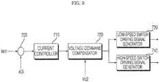
- FIG. 9 is a block diagram of the controller 550 in the power conversion device 500 according to the present disclosure.
- the controller 550 may include a calculation unit 705 for calculating a difference between an output current command value iacr and an output current ic3 flowing through the inverter 540 for first speed switching and second speed switching of the inverter 540, a current controller 710 for outputting a DC-terminal voltage command based on the difference, a voltage command compensator 720 for compensating for a voltage command based on the DC-terminal voltage command and the voltage across the DC-terminal capacitor C, a first speed switch driving signal generator 730 for outputting a first speed switching driving signal at the first switching frequency based on an output value from the voltage command compensator 720, and a second speed switch driving signal generator 740 for outputting a second speed switching driving signal at the second switching frequency based on the output value from the voltage command compensator 720.
- a calculation unit 705 for calculating a difference between an output current command value iacr and an output current ic3 flowing through the inverter 540 for first speed switching and second speed switching of the invert
- a switching control signal for operating the seventh and eighth switching elements S3 and S4 in the inverter 540 may be output through the first speed switch driving signal generator 730 and a switching control signal for operating the fifth and sixth switching elements S1 and S2 in the inverter 540 may be output through the second speed switch driving signal generator 740.
- FIG. 10 is a diagram showing driving signals applied to the gates of the fifth to eighth switching elements S1 to S4 during one cycle of an output current Vac output from the inverter 540.
- a driving signal SS3 applied to the seventh switching element S3 has a high level and thus the seventh switching element S3 can be continuously turned on.
- the controller 550 may control the fifth switching element S1 and the sixth switching element S2 to perform switching according to PWM control while the seventh switching element S3 is turned on.
- a driving signal applied to the sixth switching element S2 may be a driving signal SS2 for complementary PWM when a driving signal applied to the fifth switching element S1 is a driving signal SS1 for control PWM, as shown.
- the seventh switching element S3 and the eighth switching element S4 also complementarily operate, and thus the eighth switching element S4 is turned off while the seventh switching element S3 is turned on.
- a current path Ipath1 through the fifth switching element S1 and the eighth switching element S4 can be generated, as shown in FIG. 11A .
- a current path Ipath2 through the eighth switching element S4 and the sixth switching element S2 can be generated, as shown in FIG. 11A .
- a driving signal SS4 applied to the eighth switching element S4 has a high level and thus eighth switching element S4 can be continuously turned on.
- the controller 550 may control the sixth switching element S2 and the fifth switching element S1 to perform switching according to PWM control while eighth switching element S4 is turned on.
- the driving signal applied to the fifth switching element S1 may be a driving signal SS1 for complementary PWM when the driving signal applied to the sixth switching element S2 is a driving signal SS2 for control PWM, as shown.
- the seventh switching element S3 and the eighth switching element S4 also complementarily operate, and thus the seventh switching element S3 is turned off while the eighth switching element S4 is turned on.
- a current path Ipath3 through the seventh switching element S3 and the sixth switching element S2 can be generated, as shown in FIG. 11B .
- a current path Ipath4 through the seventh switching element S3 and the fifth switching element S1 can be generated, as shown in FIG. 11B .
- FIG. 12A is a diagram showing an inverter 540m and a filter 570m of a power conversion device 500m compared with the present disclosure.
- the inverter 540m shown in FIG. 12A is similar to that of the present application but the filter 570m differs from that of the present application in that the filter 570m is configured in a symmetrical form.
- the filter 570m shown in FIG. 12A may include first and second inductors Lm1 and Lm2 respectively provided at both terminals of the inverter 540m, and a capacitor Cm connected between the first and second inductors Lm1 and Lm2.
- some legs perform first speed switching and other legs (the fifth and sixth switching elements S1 and S2) perform second speed switching according to asynchronous PWM, as described above. Accordingly, an output current waveform Iaca and a common mode voltage waveform Vfda as shown in FIG. 12B may appear when a symmetrical filter such as the filter 570m of FIG. 12A is used.
- the present disclosure uses the asymmetrical filter 570 corresponding to the asynchronous inverter 540.
- FIG. 13A illustrates the inverter 540 and the filter 570 in the power conversion device 500 according to the present disclosure.
- the filter 570 may include an inductor Lf connected to one of the output terminals of the inverter 540, and a capacitor Cf connected between the inductor Lf and the other output terminal of the inverter 540.
- the inductor Lf is connected to only one of the output terminals of the inverter 540, a common mode voltage caused by the inverter 540 which asynchronously operates according to second speed switching and first speed switching can be considerably reduced.
- FIG. 13B shows an output current waveform Iacb and a common mode voltage waveform Vfdb according to the inverter 540 and the filter 570 shown in FIG. 13A . It can be known from the figure that the common mode voltage can be considerably reduced according to the inverter 540 and the filter 570 shown in FIG. 13A .
- controller 550 controls ripples in the voltage of the DC-terminal capacitor to decrease.
- FIG. 14A shows a system output current Iacn when control for decreasing ripples in the voltage of the DC-terminal capacitor is not performed.
- FIG. 14B shows a DC-terminal voltage waveform Vdca, a system output voltage waveform Vaca, and a system output current waveform Iaca when control for decreasing ripples in the voltage of the DC-terminal capacitor is performed.
- the DC-terminal voltage waveform Vdca has little ripples and the system output voltage waveform Vaca and the system output current waveform Iaca are hardly distorted. That is, it can be known that harmonic components THD in the system output current Iacn are removed.
- FIG. 15 is a diagram showing a power conversion device according to an embodiment of the present disclosure
- FIGS. 16 to 18B are diagrams referred to for describing the operation of FIG. 15 .
- a power conversion device 500ma may include an inverter 540 that converts DC power based on the solar cell module 100 into AC power (Vacm), and a controller 550 that controls the inverter 540.
- the inverter 540 may include fifth and sixth switching elements S1 and S2 connected to each other in series, and seventh and eighth switching elements S3 and S4 connected to the fifth and sixth switching elements S1 and S2 in parallel and connected to each other in series.
- the fifth and sixth switching elements S1 and S2 may be called first leg and the seventh and eighth switching elements S3 and S4 may be called second leg.
- the controller 550 may control the fifth and sixth switching elements S1 and S2 to perform second speed switching and may control the seventh and eighth switching elements S3 and S4 to perform first speed switching at a switching frequency lower than that of the fifth and sixth switching elements S1 and S2.
- Such a control technique may be referred to as asynchronous PWM control.
- the controller 550 may control the inverter 540 to perform the asynchronous PWM control in order to decrease the size of the power conversion device 500ma.
- the controller 550 may control the switching frequency of the seventh and eighth switching elements S3 and S4 to be same. Particularly, the controller 550 may control the switching frequency of the seventh and eighth switching elements S3 and S4 to be the same as a grid frequency. For example, it is possible to control the seventh and eighth switching elements S3 and S4 to be switched at a switching frequency of 60Hz.
- the operation efficiency of the inverter may be reduced due to a loss of conduction and a loss of switching.
- a switching frequency is varied in second speed switching of the fifth and sixth switching elements S1 and S2.
- the controller 550 may change the switching frequency of the fifth and sixth switching elements S1 and S2 in accordance with the level of the AC power Vacm output from the inverter 540.
- FIG. 16(a) is an example of an AC power waveform Vacm output from the inverter 540 and FIG. 16(b) is an example of a switching frequency waveform fm of the fifth and sixth switching elements S1 and S2.
- the AC power waveform Vacm output from the inverter 540 may be divided into a first period Pda including a zero-crossing point ZC of the AC power Vacm output from the inverter 540 in accordance with AC power, and a second period Pdb including a maximum point pka or a minimum point pkb of the AC power Vacm output from the inverter 540.
- the first period Pda including a zero-crossing point ZC of the AC power Vacm output from the inverter 540 has a defect that the loss of switching of the fifth and sixth switching elements S1 and S2 is low, but the loss of conduction is high.
- the second period Pdb including a maximum point pka or a minimum point pkb of the AC power Vacm output from the inverter 540 has a defect that the loss of conduction of the fifth and sixth switching elements S1 and S2 is low, but the loss of switching is high.
- the present disclosure proposes a method of reducing the loss of conduction in the first period Pda. Further, the present disclosure proposes a method of reducing the loss of switching in the second period Pdb.
- the controller 550 controls the switching frequency of at least some switching elements S1 and S2 in the inverter 540 in the period Pdb including a maximum point pka or a minimum point pkb of the AC power Vacm output from the inverter 540. Accordingly, in the period Pdb including a maximum point pka or a minimum point pkb of the AC power Vacm at which a loss of switching is high, the loss of switching can be reduced, so the operation efficiency of the inverter 540 can be improved.
- the controller 550 may control the switching frequency of at least some switching elements S1 and S2 in the inverter 540 to be lowest at the maximum point pka or the minimum point pkb of the AC power Vacm output from the inverter 540. Accordingly, in the period Pdb including a maximum point pka or a minimum point pkb of the AC power Vacm at which a loss of switching is high, the loss of switching can be reduced, so the operation efficiency of the inverter 540 can be improved.
- the controller 550 may control the switching frequency of some switching elements S1 and S2 in the inverter 540 in the second period Pdb to be lower than that of the first period Pda among the first period Pda including a zero-crossing point ZC of the AC power Vacm output from the inverter 540 and the second period Pdb including a maximum point pka or a minimum point pkb of the AC power Vacm output from the inverter 540.
- the controller 550 may control the fifth and sixth switching elements S1 and S2 perform second speed switching more than the seventh and eighth switching elements S3 and S4, and may control the fifth and sixth switching elements S1 and S2 of the inverter 540 to be variable in the period Pdb including a maximum point pka or a minimum point pkb of the AC power Vacm output from the inverter 540. Accordingly, it is possible to reduce a loss of switching of the switching frequency of the fifth and sixth switching elements S1 and S2, so the operation efficiency of the inverter 540 may be improved.
- the controller 550 may control the switching frequency of the seventh and eighth switching elements S3 and S4 to be the same as a grid frequency, and particularly, may control the switching frequency of the seventh and eighth switching elements S3 and S4 to be same. Accordingly, it is possible to reduce the size of the power conversion device by performing asynchronous PWM control.
- the eighth switching elements S1 ⁇ S4 in the fifth switching element may include a GaN transistor. Accordingly, it is possible to a reverse recovery loss in second speed switching.
- FIG. 17A is a diagram showing an output voltage waveform Vac and output current waveform Iacm of the inverter 540.
- An inductor current waveform Ilma corresponding to the second period Pdb1 including a maximum point pka or a minimum point pkb of the AC power Vacm output from the inverter 540 in the output voltage waveform Vac in FIG. 17A is exemplified as in FIG. 17B .
- an inductor current waveform Ilmb corresponding to the first period Pdal including a zero-crossing point ZC of the AC power Vacm output from the inverter 540 in the output voltage waveform Vac in FIG. 17A is exemplified as in FIG. 17C .
- FIG. 18A exemplifies output voltage Vacmx and output current Iacmx waveforms when the fifth and sixth switching elements S1 and S2 operate as at a fixed switching frequency
- FIG. 18B exemplifies output voltage Vacm1 and output current Iacm1 waveforms when the fifth and sixth switching elements S1 and S2 operate at a variable switching frequency.
- FIG. 19 is an exploded perspective view of the solar cell module of FIG. 1A or FIG. 1B .
- the solar cell module 100 of FIGS. 1A and 1B may include a plurality of solar cells 130.
- the solar cell module 100 may further include a first sealant 120 and a second sealant 150 provided on the upper surface and the lower surface of the solar cells 130, a rear substrate 110 provided under the first sealant 120, and a front substrate 160 provided on the second sealant 150.
- the solar cell 130 is a semiconductor device which converts solar energy into electric energy and may be a silicon solar cell, a compound semiconductor solar cell, a tandem solar cell, a dye-sensitized solar cell, a CdTe solar cell, a CIGS solar cell or a thin film solar cell.
- the solar cell 130 is formed on a light-receiving surface to which sunlight is input and a rear surface opposite the light-receiving surface.
- the solar cell 130 may include a first conductivity type silicon substrate, a second conductivity type semiconductor layer which is formed on the silicon substrate and has a conductivity type opposite the first conductivity type, an antireflection film which includes at least one opening for partially exposing the second conductivity type semiconductor layer and is formed on the second conductivity type semiconductor layer, a front electrode contacting a portion of the second conductivity type semiconductor layer exposed through the at least one opening, and a rear electrode formed on the rear side of the silicon substrate.
- the solar cells 130 may be electrically connected in series or parallel, or in serial-parallel. Specifically, the plurality of solar cells 130 may be electrically connected through the ribbon 133.
- the ribbon 133 may be attached to the front electrode formed on the light-receiving surface of a solar cell 130 and a rear electrode formed on the rear side of a neighboring solar cell 130.
- the figure shows that the ribbon 133 is formed in two lines and the solar cells 130 are connected in a row through the ribbon 133 to form a solar cell string 140.
- each string may include ten solar cells, as described above with reference to FIG. 2 .
- the rear substrate 110 is a back sheet and serves to execute waterproofing, insulation and sunblocking functions.
- the rear substrate 110 may be a Tedlar/PET/Tedlar (TPT) type but the present disclosure is not limited thereto.
- TPT Tedlar/PET/Tedlar
- the rear substrate 110 is rectangular in FIG. 4 , the rear substrate 110 may be manufactured in various forms such as a circle and a semicircle according to environment in which the solar cell module 100 is installed.
- the first sealant 120 may be attached to the rear substrate 110 having the same size as the rear substrate 110, and a plurality of solar cells 130 may be arranged in several rows on the first sealant 120.
- the second sealant 150 is positioned on the solar cells 130 and attached to the first sealant 120 through lamination.
- first sealant 120 and the second sealant 150 are used to chemically connect elements of the solar cells.
- Various materials such as ethylene vinyl acetate (EVA) film may be used as the first sealant 120 and the second sealant 150.
- EVA ethylene vinyl acetate
- the front substrate 160 is positioned on the second sealant 150 such that sunlight is transmitted through the front substrate 160. It is desirable that the front substrate 160 be tempered glass in order to protect the solar cells 130 from external impact. It is more desirable that the front substrate 160 be low-iron tempered glass in order to prevent reflection of sunlight and to improve transmissivity of sunlight.
- the photovoltaic module according to the present disclosure is not limited to the above-described embodiments and all or some of the embodiments may be selectively combined such that the embodiments can be modified in various manners.
- the photovoltaic module includes: a solar cell module including a plurality of solar cells; a converter to convert a level of a DC power input from the solar cell module; an inverter to convert the DC power into an AC power; and a controller to control the inverter, in which the controller performs asynchronous pulse width modulation control for the inverter, and controls a switching frequency of at least some switching elements in the inverter to be changed for a period including a maximum point or a minimum point of the AC power output from the inverter. Accordingly, it is possible to reduce a loss of switching in a period including a maximum point or a minimum point of AC power at which a loss of switching is high, so operation efficiency of the inverter can be improved.
- the controller controls a switching frequency of at least some switching elements in the inverter to be lowest at the maximum point or the minimum point of the AC power output from the inverter. Accordingly, it is possible to reduce a loss of switching in a period including a maximum point or a minimum point of AC power at which a loss of switching is high, so operation efficiency of the inverter can be improved.
- the controller controls the switching frequency of at least some switching elements in the inverter in the second period to be lower than that of the first period among the first period including a zero-crossing point of the AC power output from the inverter and the second period including a maximum point or a minimum point of the AC power output from the inverter. Accordingly, in the second period including a maximum point or a minimum point of the AC power at which a loss of switching is high, the loss of switching can be reduced. Further, in the first period including a maximum point or a minimum point of the AC power at which a loss of conduction is high, a loss of conduction can be reduced, so operation efficiency of the inverter can be improved.
- the controller controls the first and second switching elements to perform second speed switching more than the third and fourth switching elements, and controls a switching frequency of the first and second switching elements of the inverter to be changed for a period including a maximum point or a minimum point of the AC power output from the inverter. Accordingly, it is possible to reduce a loss of switching of the switching frequency of the first and second switching elements, so the operation efficiency of the inverter may be improved.
- the controller can control the switching frequency of the third and fourth switching elements to be the same as a grid frequency, and particularly, the switching frequency of the third and fourth switching elements to be same. Accordingly, it is possible to reduce the size of the power conversion device by performing asynchronous pulse width-variable control.
- the first switching element to the fourth switching element may include a gallium nitride (GaN) transistor. Accordingly, it is possible to a reverse recovery loss in second speed switching.
- GaN gallium nitride
Landscapes
- Engineering & Computer Science (AREA)
- Power Engineering (AREA)
- Life Sciences & Earth Sciences (AREA)
- Sustainable Development (AREA)
- Sustainable Energy (AREA)
- Physics & Mathematics (AREA)
- Electromagnetism (AREA)
- General Physics & Mathematics (AREA)
- Radar, Positioning & Navigation (AREA)
- Automation & Control Theory (AREA)
- Inverter Devices (AREA)
- Dc-Dc Converters (AREA)
Description
- The present disclosure relates to a photovoltaic module and, more particularly, to a photovoltaic module that can improve operation efficiency of an inverter.
- A photovoltaic module means a state in which solar cells for solar photovoltaic power generation are connected in series or in parallel.
- Meanwhile, a converter of a photovoltaic module performs maximum power point follow-up control. Meanwhile, various plans that can improve operation efficiency of an inverter in accordance with variations of input voltage that is input to the converter of a photovoltaic module are studied.
-
US 2018/191273 A1 relates to a three-level inverter switching method and inFIG. 2 , an optional boost converter 210, an optional isolation transformer 220, an inverter 230, an output filter 240, an optional driver circuit 270, a driver circuit 260, an output sensor 250, a microcontroller 280, and a power supply 290 are disclosed. Referring toFigs. 3 and7 , Hysteresis current control pulse-width modulation (PWM) is illustrated. -
US 2016/315556 A1 relates to a method for acquiring values indicative of an ac current of an inverter and related circuit and inverter. InFigs. 6 and7 , a first predetermined switching period TSW1, and a second predetermined switching period TSW2 are disclosed. -
JP 2016 010258 A power conversion device 1 includes a power circuit 7 and acontrol device 8 and the power circuit 7 includes aDC filter circuit 11, an inverter circuit 12, a reactor circuit 13 and an AC filter circuit 14 inFig. 7 . -
JP H06 245538 A -
JP 2011 109739 A - The document "A grid-tied power factor corrector microinverter without electrolytic capacitor by the control of voltage in a DC-link for a non-linear load" by Moreno Frank A et al., 2017 14th international conference on electrical engineering, computing science and automatic control, IEEE, 2017-10-20, pages 1-6, XP033256429 illustrates a DC/DC converter, a DC/AC converter and a TAB controller in
Fig. 1 . - An object of the present disclosure is to provide a photovoltaic module according to
independent claim 1, that can improve operation efficiency of an inverter. - Another object of the present disclosure is to provide a photovoltaic module that can reduce the size of a power conversion device.
- In order to achieve the objects, a photovoltaic module according to the present disclosure includes: a solar cell module including a plurality of solar cells; a converter to convert a level of a DC power input from the solar cell module; an inverter to convert the DC power into an AC power; and a controller to control the inverter, in which the controller performs asynchronous pulse width modulation control for the inverter, and controls a switching frequency of at least some switching elements in the inverter to be changed for a period including a maximum point or a minimum point of the AC power output from the inverter.
- The controller controls a switching frequency of at least some switching elements in the inverter to be lowest at the maximum point or the minimum point of the AC power output from the inverter.
- The controller controls the switching frequency of at least some switching elements in the inverter in the second period to be lower than that of the first period among the first period including a zero-crossing point of the AC power output from the inverter and the second period including a maximum point or a minimum point of the AC power output from the inverter.
- The inverter includes: first and second switching elements connected to each other in series; and third and fourth switching elements connected to the first and second switching elements in parallel and connected to each other in series.
The controller may control the first and second switching elements to perform second speed switching more than the third and fourth switching elements, and may control a switching frequency of the first and second switching elements of the inverter to be changed for a period including a maximum point or a minimum point of the AC power output from the inverter. - The controller may control a switching frequency of the third and fourth switching elements to be the same as a grid frequency.
- The controller may control a switching frequency of the third and fourth switching elements to be same.
- The first switching element to the fourth switching element may include a gallium nitride (GaN) transistor.
-
-
FIG. 1A is a diagram showing an example of a photovoltaic system including a photovoltaic module according to an embodiment of the present disclosure; -
FIG. 1B is a diagram showing another example of a photovoltaic system including a photovoltaic module according to an embodiment of the present disclosure; -
FIG. 2 is a diagram showing an internal circuit of the junction box in the photovoltaic module ofFIG. 1A orFIG. 1B ; -
FIGS. 3A to 3B are a circuit diagram of a power conversion device included in a photovoltaic module related to the present disclosure; -
FIG. 4 is a circuit diagram of a power conversion device in the photovoltaic module according to an embodiment of the present disclosure; -
FIGS. 5 to 7 are diagrams referred to for describing the power conversion device ofFIG. 4 ; -
FIG. 8 is a flowchart illustrating a method of operating the photovoltaic module according to an embodiment of the present disclosure; -
FIGS. 9 to 14B are diagrams referred to for describing the power conversion device ofFIG. 4 ; -
FIG. 15 is a diagram showing a power conversion device according to an embodiment of the present disclosure; -
FIGS. 16 to 18B are diagrams referred to for describing the operation ofFIG. 15 ; and -
FIG. 19 is an exploded perspective view of the solar cell module ofFIG. 1A orFIG. 1B . - In this embodiment, a plan that can reduce a ripple of an input current that is input to a converter in a photovoltaic module.
- The present disclosure proposes a method for reducing ripples in current input to a converter in a photovoltaic module.
- The present disclosure will be described in more detail with reference to the drawings.
- The suffixes "module" and "unit" of elements herein are used for convenience of description and do not have any distinguishable meanings or functions. Accordingly, the suffixes "module" and "unit" can be used interchangeably.
-
FIG. 1A is a diagram showing an example of a photovoltaic system including a photovoltaic module according to an embodiment of the present disclosure. - Referring to
FIG. 1A , a photovoltaic system 10a according to an embodiment of the present disclosure may include aphotovoltaic module 50 and agateway 80. - The
photovoltaic module 50 may integrally include asolar cell module 100 and ajunction box 200 including a power conversion device (500 inFIG. 4 ) which converts DC power in the solar cell module and outputs the converted power. - Although the
junction box 200 is attached to the rear side of thesolar cell module 100 in the figure, the present disclosure is not limited thereto. Thejunction box 200 may be separate from thesolar cell module 100. - A cable oln for supplying AC power output from the
junction box 200 to agrid 90 may be electrically connected to an output terminal of thejunction box 200. - The
gateway 80 may be positioned between one or more power conversion device and thegrid 90. Thegateway 80 may detect an alternating current (AC) io and an AC voltage vo output from thephotovoltaic module 50 through the cable oln. Thegateway 80 may output a power factor adjustment signal for power factor adjustment based on a phase difference between the AC io and the AC voltage vo output from thephotovoltaic module 50. To this end, thegateway 80 and thephotovoltaic module 50 may perform power line communication (PLC) using acable 323. - The power conversion device (500 in
FIG. 4 ) included in thephotovoltaic module 50 may convert DC power output from thesolar cell module 100 into AC power and output the AC power. To this end, the power conversion device (500 inFIG. 4 ) in thephotovoltaic module 50 may include a converter (530 inFIG. 6 ) and an inverter (540 inFIG. 4 ). - The power converter (500 in
FIG. 4 ) may be called a micro-inverter. Accordingly, the micro-inverter may include a converter (530 inFig. 4 ) and an inverter (540 inFig. 4 ). - In the present disclosure, a 2-stage power conversion device which converts the level of DC power output from the
solar cell module 100 through theconverter 530 included in the power conversion device (500 inFIG. 4 ) or the micro-inverter, and then performs AC power conversion through theinverter 540 is described. - The present invention proposes a method for performing power conversion with high voltage boost and high efficiency through the
converter 530 in the 2-stage power conversion device. - To this end, the
photovoltaic module 50 according to an embodiment of the present disclosure may include thesolar cell module 100, theconverter 530, and acontroller 550. Thephotovoltaic module 50 according to an embodiment of the present disclosure may further include theinverter 540. - The
converter 530 in thepower conversion device 500 according to an embodiment of the present disclosure may include a full-bridge switching unit 532 which switches DC power, atransformer 536 having an input side connected to an output terminal of the full-bridge switching unit 532, asynchronous rectifier 538 connected to an output side of thetransformer 536, and a resonant capacitor Cr and a resonant inductor Lr which are connected between thetransformer 536 and thesynchronous rectifier 538. Thecontroller 550 may perform power conversion with high voltage boost and high efficiency by changing a switching frequency of the full-bridge switching unit 532 and thesynchronous rectifier 538 which is a half-bridge switching unit based on the input voltage of theconverter 530 or the voltage of a DC-terminal capacitor C. - Particularly, the
controller 550 may control phase shift of the full-bridge switching unit 532 such that the full-bridge switching unit 532 operates in a buck mode and control the full-bridge switching unit 532 and thesynchronous rectifier 538 to operate at a first switching frequency when the voltage of the DC-terminal capacitor C is equal to or higher than a target voltage, and may control duty of thesynchronous rectifier 538 which is a half-bridge switching unit such that thesynchronous rectifier 538 operates in a boost mode and the full-bridge switching unit 532 and thesynchronous rectifier 538 operate at a second switching frequency lower than the first switching frequency when the voltage of the DC-terminal capacitor C is lower than the target voltage, thereby performing power conversion with high voltage boost and high efficiency. - Here, the first and second switching frequencies may be much higher than a grid frequency, and thus the sizes of circuit elements in the
converter 530 can be reduced. - Particularly, the turn ratio of the
transformer 536 can be reduced and thus the size of thetransformer 536 can be decreased. Consequently, the size of theconverter 530 used in thephotovoltaic module 50 can be reduced. - Control is performed such that ripples in the voltage of the DC-terminal capacitor C are reduced, and thus a film capacitor instead of an electrolytic capacitor can be used as the DC-terminal capacitor C. Accordingly, the size of the DC-terminal capacitor C can be reduced.
- When the voltage of the DC-terminal capacitor is equal to or higher than the target voltage, the full-
bridge switching unit 532 may be controlled to enter the buck mode in which a phase difference between switching elements in the full-bridge switching unit 532 increases as the difference between the voltage of the DC-terminal capacitor and the target voltage increases such that the voltage of the DC-terminal capacitor follows the target voltage. - When the voltage of the DC-terminal capacitor is lower than the target voltage, the
synchronous rectifier 538 is controlled to enter the boost mode in which turn-on duty of switching elements in thesynchronous rectifier 538 increases as the difference between the voltage of the DC-terminal capacitor and the target voltage increases such that the voltage of the DC-terminal capacitor follows the target voltage. - Meanwhile, the
converter 530 in thepower conversion device 500 according to another embodiment of the present disclosure may include the full-bridge switching unit 532 which switches DC power, thetransformer 536 having an input side connected to the output terminal of the full-bridge switching unit 532, thesynchronous rectifier 538 connected to the output side of thetransformer 536, and the resonant capacitor Cr and the resonant inductor Lr connected between thetransformer 536 and thesynchronous rectifier 538. Thecontroller 550 may control the full-bridge switching unit 532 to operate in the buck mode or boost mode depending on the voltage level of the DC-terminal capacitor C, thereby performing power conversion with high voltage boost and high efficiency. - The
inverter 540 in thepower conversion device 500 according to an embodiment of the present disclosure includes a plurality of switching elements S1 to S4 and converts DC power from a DC-terminal capacitor C into AC power. Some of the plurality of switching elements S1 to S4 may perform switching at a third switching frequency and other switching elements may perform switching at a forth switching frequency. - That is, the
controller 550 may control some of the switching elements S1 to S4 to perform switching at the thied switching frequency and control other switching elements to perform switching at the forth switching frequency. - Here, the third switching frequency may correspond to a grid frequency and the forth switching frequency may be higher than the grid frequency.
- Accordingly, second speed switching is performed with respect to some switching elements in the
inverter 540 and thus not only the size of theinverter 540 but also the sizes of other circuit elements in the power conversion device can be reduced according to a high switching frequency. - The other switching elements among the switching elements S1 to S4 may include GaN transistors or SiC transistors and thus reverse recovery loss during second speed switching can be reduced.
- Further, a
filter 570 provided at output terminals of theinverter 540 includes an inductor connected to one of the output terminals of theinductor 540 and a capacitor connected between the inductor and the other output terminal of theinverter 540. Accordingly, a common mode voltage at the output terminals of theinverter 540 can be reduced. Furthermore, a harmonic component THD of output current can be reduced. - The
controller 550 may perform power conversion with high voltage boost and high efficiency by changing a switching frequency of a full-bridge switching unit 532 based on the input voltage of theconverter 530 or the voltage of the DC-terminal capacitor C. - Particularly, the
controller 550 may control the full-bridge switching unit 532 to enter a buck mode and operate at a first switching frequency when the voltage of the DC-terminal capacitor C is equal to or higher than a target voltage and control the full-bridge switching unit 532 to enter a boost mode and operate at a second switching frequency lower than the first switching frequency when the voltage of the DC-terminal capacitor C is lower than the target voltage, thereby performing power conversion with high voltage boost and high efficiency. - Here, the third and fourth switching frequencies may be much higher than the grid frequency. Accordingly, the sizes of circuit elements in the
converter 530 can be reduced. - Particularly, the turn ratio of a
transformer 536 can be reduced, and thus the size of thetransformer 536 can be decreased. Consequently, the size of theconverter 530 used in thephotovoltaic module 50 can be reduced. - Control is performed such that ripples in the voltage of the DC-terminal capacitor C are reduced, and thus a film capacitor instead of an electrolytic capacitor can be used as the DC-terminal capacitor C. Accordingly, the size of the DC-terminal capacitor C can be reduced.
- When the voltage of the DC-terminal capacitor is equal to or higher than the target voltage, the full-
bridge switching unit 532 may be controlled to enter the buck mode in which a phase difference between switching elements in the full-bridge switching unit 532 increases as the difference between the voltage of the DC-terminal capacitor and the target voltage increases such that the voltage of the DC-terminal capacitor follows the target voltage. - When the voltage of the DC-terminal capacitor is lower than the target voltage, a
synchronous rectifier 538 may be controlled to enter the boost mode in which turn-on duty of switching elements in thesynchronous rectifier 538 increases as the difference between the voltage of the DC-terminal capacitor and the target voltage increases such that the voltage of the DC-terminal capacitor follows the target voltage. - Meanwhile, the
converter 540 in thepower conversion device 500 according to another embodiment of the present disclosure is driven according to asynchronous PWM. Accordingly, the sizes of circuit elements in the power conversion device can be reduced. -
FIG. 1B is a diagram showing another example of a photovoltaic system including a photovoltaic module according to an embodiment of the present disclosure. - Referring to
FIG. 1B , aphotovoltaic system 10b according to an embodiment of the present disclosure may include a plurality ofphotovoltaic modules 50a, 50b, ..., 50n and thegateway 80. - The
photovoltaic system 10b ofFIG. 1B differs from the photovoltaic system 10a ofFIG. 1A in that thephotovoltaic modules 50a, 50b, ..., 50n are connected in parallel. - The
photovoltaic modules 50a, 50b, ..., 50n may respectively includesolar cell modules 100a, 100b, ..., 100n andjunction boxes - Although the
junction boxes solar cell modules 100a, 100b, ..., 100n in the figure, the present disclosure is not limited thereto. Thejunction boxes solar cell modules 100a, 100b, ..., 100n. - Further,
cables junction boxes grid 90 may be electrically connected to output terminals of thejunction boxes - As described above with reference to
FIG. 1A , theconverter 530 in thepower conversion device 500 included in each of thephotovoltaic modules 50a, 50b, ... 50n may include a full-bridge switching unit 532 which switches DC power, atransformer 536 having an input side connected to an output terminal of the full-bridge switching unit 532, asynchronous rectifier 538 connected to an output side of thetransformer 536, and a resonant capacitor Cr and a resonant inductor Lr which are connected between thetransformer 536 and thesynchronous rectifier 538. Thecontroller 550 may perform power conversion with high voltage boost and high efficiency by changing a switching frequency of the full-bridge switching unit 532 and thesynchronous rectifier 538 which is a half-bridge switching unit based on the input voltage of theconverter 530 or the voltage of a DC-terminal capacitor C. - In the
inverter 540 included in thepower conversion device 500 included in each of thephotovoltaic modules 50a, 50b, ... 50n shown inFIG. 1B , some of the switching elements S1 to S4 may perform switching at the third switching frequency and other switching elements may perform switching at the forth frequency higher than the third switching frequency, as described above with referent toFIG. 1A . Accordingly, the size of the power conversion device can be reduced. - Particularly, since switching is performed at the third switching frequency corresponding to the grid frequency and the forth switching frequency higher than the third switching frequency, second speed switching effect is obtained and thus not only the size of the
inverter 540 but also the sizes of circuit elements in the power conversion device including theinverter 540 can be reduced. -
FIG. 2 is a diagram showing an internal circuit of the junction box in the photovoltaic module ofFIG. 1A orFIG. 1B . - Referring to the figure, the
junction box 200 may convert DC power from thesolar cell module 100 and output the converted power. - Particularly, the
junction box 200 according to the present disclosure may include the power conversion device (500 inFIG. 4 ) for outputting AC power. - To this end, the
junction box 200 may include theconverter 530, theinverter 540 and thecontroller 550 for controlling the same. - In addition, the
junction box 200 may further include abypass diode unit 510 for bypass, acapacitor unit 520 for storing DC power, and afilter 570 for filtering output AC power. - The
junction box 200 may further include acommunication device 580 for communication with theexternal gateway 80. - In addition, the
junction box 200 may further include an input current detector A, an input voltage detector B, a converter output current detector C, a converter output voltage detector D, an inverter output current detector E and an inverter output voltage detector F. - The
controller 550 may control theconverter 530, theinverter 540 and thecommunication device 580. - The
bypass diode unit 510 may include the bypass diodes Dc, Db and Da arranged between the first to fourth conductive lines (not shown) of thesolar cell module 100. Here, the number of bypass diodes is one or more, preferably, less than the number of conductive lines by one. - The bypass diodes Dc, Db and Da receive photovoltaic DC power from the
solar cell module 100, particularly, from the first to fourth conductive lines (not shown) in thesolar cell module 100. When a reverse voltage is generated in DC power from at least one of the first to fourth conductive lines (not shown), the bypass diodes Dc, Db and Da may bypass the DC power. - DC power which has passed through the
bypass diode unit 510 may be input to thecapacitor unit 520. - The
capacitor unit 520 may store the DC power input through thesolar cell module 100 and thebypass diode unit 510. - Although the figure shows that the
capacitor unit 520 includes a plurality of capacitors Ca, Cb and Cc connected in parallel, a plurality of capacitors may be connected in series and parallel or connected in series to a ground terminal. Alternatively, thecapacitor unit 520 may include only one capacitor. - The
converter 530 may convert the level of an input voltage from thesolar cell module 100, which has passed through thebypass diode unit 510 and thecapacitor unit 520. - Particularly, the
converter 530 may perform power conversion using DC power stored in thecapacitor unit 520. - The
converter 530 according to an embodiment of the present disclosure will be described in more detail with reference toFIG. 4 . - Switching elements in the
converter 530 may be turned on/off based on a converter switching control signal from thecontroller 550. Accordingly, level-converted DC power can be output. - The
inverter 540 may convert the DC power converted by theconverter 530 into AC power. - The figure shows a full-bridge inverter. That is, upper arm switching elements S1 and S3 connected in series and lower arm switching elements S2 and S4 connected in series are paired, and the two pairs of upper and lower arm switching elements S1, S2, S3 and S4 are connected in parallel. A diode may be connected in anti-parallel with each switching element S1 to S4.
- The switching elements S1 to S4 in the
inverter 540 may be turned on/off based on an inverter switching control signal from thecontroller 550. Accordingly, AC power having a predetermined frequency can be output. Desirably, AC power having the same frequency (about 60 Hz or 50 Hz) as the AC frequency of the grid is output. - The capacitor C may be disposed between the
converter 530 and theinverter 540. - The capacitor C may store the DC power having the level converted by the
converter 530. Both terminals of the capacitor C may be called DC terminals and thus the capacitor C may be called a DC-terminal capacitor. - The input current detector A may detect input current ic1 supplied from the
solar cell module 100 to thecapacitor unit 520. - The input voltage detector B may detect an input voltage Vc1 supplied from the
solar cell module 100 to thecapacitor unit 520. Here, the input voltage Vc1 may be the same as the voltage stored in thecapacitor unit 520. - The detected input current ic1 and input voltage vc1 may be input to the
controller 550. - The converter output current detector C detects output current ic2 from the
converter 530, that is, DC-terminal current, and the converter output voltage detector D detects an output voltage vc2 from theconverter 530, that is, a DC-terminal voltage. The detected output current ic2 and output voltage vc2 may be input to thecontroller 550. - The inverter output current detector E detects current ic3 output from the
inverter 540 and the inverter output voltage detector F detects a voltage vc3 output from theinverter 540. The detected current ic3 and voltage vc3 are input to thecontroller 550. - The
controller 550 may output control signals for controlling the switching elements of theconverter 530. Particularly, thecontroller 550 may output a turn-on timing signal of the switching elements included in theconverter 530 based on at least one of the detected input current ic1, input voltage vc1, output current ic2, output voltage vc2, output current ic3 and output voltage vc3. - Further, the
controller 550 may output inverter control signals for controlling the switching elements S1 to S4 of theinverter 540. Particularly, thecontroller 550 may output a turn-on timing signal of the switching elements S1 to S4 of theinverter 540 based on at least one of the detected input current ic1, input voltage vc1, output current ic2, output voltage vc2, output current ic3 or output voltage vc3. - Further, the
controller 550 may calculate a maximum power point with respect to thesolar cell module 100 and control theconverter 530 to output DC power corresponding to maximum power according thereto. - The
communication device 580 may perform communication with thegateway 80. - For example, the
communication device 580 may exchange data with thegateway 80 through power line communication. - The
communication device 580 may transmit current information, voltage information and power information of thephotovoltaic module 50 to thegateway 80. - The
filter 570 may be disposed at the output terminals of theinverter 540. - In addition, the
filter 570 may include a plurality of passive elements and adjust a phase difference between an AC io and an AC voltage vo output from theinverter 540 based on at least some of the plurality of passive elements. -
FIGS. 3A and 3B are circuit diagrams of power conversion devices included in a photovoltaic module related to the present disclosure. - A
power conversion device 500x included in the photovoltaic module shown inFIG. 3A includes a full-bridge switching unit 532x, atransformer 536x and asynchronous rectifier 538x. - In the
synchronous rectifier 538x included in thepower conversion device 500x of the photovoltaic module, a diode D1 and a switching element Q5 are connected in series, a diode D2 and a switching element Q6 are connected in series, and the two pairs of the diodes and switching elements are connected in parallel. - According to the
power conversion device 500x included in the photovoltaic module ofFIG. 3A , the turn ratio of thetransformer 536x needs to be considerably high, approximately 1:12, when high voltage boost is required according to variation in an input voltage Vpv. That is, thetransformer 536x having a high turn ratio needs to be used. Furthermore, an additional leakage inductor is required. Accordingly, the size of thetransformer 536x increases, thus increasing the volume of thepower conversion device 500x. - A
power conversion device 500y in the photovoltaic module shown inFIG. 3B includes a full-bridge switching unit 532y, atransformer 536y, asynchronous rectifier 538y, a resonant capacitor Cr and a resonant inductor Lr between the full-bridge switching unit 532y and thetransformer 536y. - According to the
power conversion device 500y included in the photovoltaic module ofFIG. 3B , thetransformer 536y needs to have a high turn ratio although the resonant capacitor Cr and the resonant inductor Lr are provided at the primary side of thetransformer 536y. Accordingly, the size of thetransformer 536y increases, thus increasing the volume of thepower conversion device 500y. - The present disclosure proposes a method for reducing the size of the transformer while performing power conversion with high voltage boost and high efficiency. Particularly, the present disclosure proposes a method for reducing the sizes of circuit elements in the converter by increasing a switching frequency of the full-
bridge switching unit 532 and thesynchronous rectifier 538 which is a half-bridge switching unit. This will be described with reference toFIG. 4 and the following figures. -
FIG. 4 is a circuit diagram of the power conversion device in the photovoltaic module according to an embodiment of the present disclosure andFIGS. 5 to 7 are diagrams referred to for describing the power conversion device ofFIG. 4 . - Referring to the figures, the
power conversion device 500 in thephotovoltaic module 100 according to an embodiment of the present disclosure may include thebypass diode unit 510, thecapacitor unit 520, thecontroller 550, thecommunication device 580, the input current detector A, the input voltage detector B, the converter output current detector C, the converter output voltage detector D, the inverter output current detector E and the inverter output voltage detector F, which are shown inFIG. 4 , in addition to theconverter 530 and theinverter 540. - Meanwhile, to reduce electromagnetic noise, the
filter 570 for filtering AC power output from theinverter 540 may be provided at the output terminals of theinverter 540. - The
filter 570 may include first and second inductor L1 and L2 connected to both output terminals of theinverter 530, respectively, and a capacitor C4 connected between the first inductor L1 and the second inductor L2. - Accordingly, the
filter 570 is realized in an asymmetrical form in consideration of theinverter 540 operating according to asynchronous PWM control, and thus a common mode voltage at the output terminals of theinverter 540 can be reduced and a harmonic component THD of output current can be reduced. - The following description focuses on the
converter 530 shown inFIG. 4 . - The
power conversion device 500 in thephotovoltaic module 50 according to an embodiment of the present disclosure may include theconverter 530 which converts the level of DC power input from thesolar cell module 100, and the DC-terminal capacitor C which stores DC power output from theconverter 530. - The
power conversion device 500 in thephotovoltaic module 100 according to an embodiment of the present disclosure may further include theinverter 570 which converts the DC power from the DC-terminal capacitor C into AC power. - The
converter 530 according to an embodiment of the present disclosure may include the full-bridge switching unit 532 which switches DC power, thetransformer 536 having the input side connected to the output terminal of the full-bridge switching unit 532, thesynchronous rectifier 538 connected to the output side of thetransformer 536, the resonant capacitor Cr and the resonant inductor Lr which are connected between thetransformer 536 and thesynchronous rectifier 538. - Particularly, ripples in input current can be reduced according to resonance of the resonant capacitor Cr, the resonant inductor Lr and the
transformer 536. - Switching elements Q1 to Q4 in the full-
bridge switching unit 532 can perform zero-voltage switching ZVS and zero-current switching ZCS according to the resonant capacitor Cr and the resonant inductor Lr. - As shown, the full-
bridge switching unit 532 may include the first and second switching elements Q1 and Q2 connected in series, and the third and fourth switching elements Q3 and Q4 respectively connected in parallel with the first and second switching elements Q1 and Q2. - In addition, the input terminals na and nb of the
transformer 536 may be connected between a first node n1 between the first and second switching elements Q1 and Q2 and a second node n2 between the third and fourth switching elements Q3 and Q4. - The
inverter 540 may include fifth and sixth switching elements S1 and S2 connected in series, and seventh and eighth switching elements S3 and S4 connected in series. - AC power can be output through a fifth node n5 between the fifth and sixth switching elements S1 and S2 and a sixth node n6 between seventh and eighth switching elements S3 and S4.
- As shown, the
synchronous rectifier 538 may include ninth and tenth switching elements Q9 and Q10 connected in series, and first and second capacitors C1 and C2 connected in series. - Here, the ninth and tenth switching elements Q9 and Q10 may be connected in parallel with the first and second capacitors C1 and C2.
- The output side of the
transformer 536 may be connected between a third node n3 between the ninth and tenth switching elements Q9 and Q10 and a fourth node n4 between the first and second capacitors C1 and C2. - Meanwhile, the
synchronous rectifier 538 is configured in a half bridge form and thus may be called a half-bridge switching unit. - The
synchronous rectifier 538 amplifies an input voltage twice and outputs the amplified voltage and thus may be called a voltage doubler. - The
controller 550 may control theconverter 530 and theinverter 540 together. - . Particularly, the
controller 550 may output a control signal Sfb to the full-bridge switching unit 532 included in theconverter 530 for maximum power point tracking control. - The
controller 550 may output a control signal Shb to thesynchronous rectifier 538 in order to control the same. - Further, the
controller 550 may output a control signal Sic to theinverter 540 in order to control the same. - The
controller 550 may change the switching frequency of the full-bridge switching unit 532 based on the input voltage of theconverter 530 or the voltage of the DC-terminal capacitor C. - Specifically, the
controller 550 may control the full-bridge switching unit 532 to operate in the buck mode or boost mode depending on the voltage level of the DC-terminal capacitor C. - The
controller 550 may control the full-bridge switching unit 532 to operate in the buck mode when the voltage of the DC-terminal capacitor C is equal to or higher than a target voltage and control thesynchronous rectifier 538 of half-bridge switching unit to operate in the boost mode when the voltage of the DC-terminal capacitor C is lower than the target voltage. - The
controller 550 may control the full-bridge switching unit 532 to enter the buck mode and operate at a first switching frequency (1/Tsa = Fsa inFIG. 5 ) when the voltage of the DC-terminal capacitor C is equal to or higher than the target voltage, and may control thesynchronous rectifier 538 of half-bridge switching unit to operate in the boost mode, and may control the full-bridge switching unit 532 and thesynchronous rectifier 538 to operate at a second switching frequency (1/Tsb = Fsb inFIG. 6 ) lower than the first switching frequency (1/Tsa = Fsa inFIG. 5 ) when the voltage of the DC-terminal capacitor C is lower than the target voltage. - It is desirable that the switching frequency of the full-
bridge switching unit 532 be higher than a grid frequency. - For example, the first switching frequency may be 135 kHz and the second switching frequency may be 90 kHz. Accordingly, second speed switching is performed and thus the sizes of the circuit elements in the
converters 530 can be reduced. Particularly, the size of thetransformer 536 can be reduced. - The
controller 550 can control ripples in the voltage of the DC-terminal capacitor C to decrease through the buck mode or boost mode. - Further, the
controller 550 may control some of the switching elements S1 to S4 in theinverter 540 to perform switching at the third switching frequency and control other switching elements to perform switching at the forth switching frequency higher than the third switching frequency. - That is, the
controller 550 may perform asynchronous PWM control for theinverter 540. - Here, the third switching frequency corresponds to the grid frequency and the forth switching frequency is higher than the third switching frequency, and thus the
inverter 540 can perform second speed switching. Accordingly, the sizes of circuit elements in the power conversion device can be reduced, thus decreasing the size of the power conversion device. - The
controller 550 may control the fifth and sixth switching elements S1 and S2 to operate at the forth switching frequency and control the seventh and eighth switching elements S3 and S4 to operate at the third switching frequency. - Further, the
controller 550 may control the fifth and sixth switching elements S1 and S2 to perform switching according to PWM control while the seventh switching element S3 is turned on and control the sixth and fifth switching elements S2 and S1 to perform switching according to PWM control while the eighth switching element S4 is turned on. - Meanwhile, it is desirable that some S3 and S4 of the switching elements S1 to S4 included in the
inverter 540 and others S1 and S2 of the switching elements S1 to S4 be switching elements of different types. - The switching elements S1 and S2 among the switching elements S1 to S4 in the
inverter 540, for example, switching elements performing second speed switching, may include GaN transistors or SiC transistors. Accordingly, reverse recovery loss during second speed switching can be reduced. - The switching elements S3 and S4 among the switching elements S1 to S4 in the
inverter 540, for example, switching elements performing first speed switching, may include metal-oxide-semiconductor field-effect-transistors (MOSFETs). -
FIG. 5 is a diagram referred to for describing a case in which the fullbridge switching unit 532 operates in the buck mode. -
FIG. 5(a) shows a waveform Vdca of the DC-terminal voltage which is the voltage of the DC-terminal capacitor C. -
FIG. 5(b) shows switching control signals SQ1 and SQ4 applied to the gates of the first switching element Q1 and the fourth switching element Q4. -
FIG. 5(c) shows switching control signals SQ2 and SQ3 applied to the gates of the second switching element Q2 and the third switching element Q3. -
FIG. 5(d) shows a voltage waveform VQ4 and a current waveform IQ4 applied to the fourth switching element Q4. - In the buck mode, the first and fourth switching elements Q1 and Q4 are not alternately turned on and the second and third switching elements Q2 and Q3 are not alternately turned on in the full-
bridge switching unit 532 and turn-on periods thereof may partially overlap according to phase shift as shown. - That is, a phase difference between the first switching element Q1 and the fourth switching element Q4 is not fixed to 180 degrees and phases or turn-on timing may be varied according to phase shift.
- The figure shows that the phase difference between the first switching element Q1 and the fourth element Q4 is DLa.
- The
controller 550 may control the full-bridge switching unit 532 to operate at a maximum switching frequency and change the phase difference DLa between switching elements in the full-bridge switching unit 532 in the buck mode. - When the voltage of the DC-terminal capacitor C is equal to or higher than a target voltage, the
controller 550 may control the phase difference DLa between switching elements in the full-bridge switching unit 532 to increase as the difference between the voltage of the DC-terminal capacitor C and the target voltage increases. - Particularly, the
controller 550 may control the phase difference DLa between the first switching element Q1 and the fourth switching element Q4 to increase as the difference between the voltage of the DC-terminal capacitor C and the target voltage increases. - The
controller 550 may control turn-on timing of the fourth and third switching elements Q4 and Q3 in the full-bridge switching unit 532 to be delayed from turn-on timing of the first and second switching elements Q1 and Q2 in the buck mode. Accordingly, the DC-terminal voltage Vda can be varied. - For example, when the first and fourth switching elements Q1 and Q4 are turned on, current flows and thus the resonant capacitor Cr and the resonant inductor Lr resonate.
- Thereafter, when the fourth switching element A4 is turned off and the third switching element Q3 is turned on, the current flowing through the
transformer 536 decreases to the ground GND or zero, theconverter 530 operates in a discontinue mode (DCM) and a secondary switch may perform zero-current switching (ZCS). - The switching elements Q9 and Q10 in the
synchronous rectifier 538 may be switched in synchronization with the first and second switching elements Q1 and Q2 in the full-bridge switching unit 532. - The
controller 550 may control turn-on timing delay to increase as the difference between the voltage of the DC-terminal capacitor C and the target voltage increases when the voltage of the DC-terminal capacitor C is equal to or higher than the target voltage. - Accordingly, the difference between the voltage of the DC-terminal capacitor C and the target voltage can be reduced, and thus the DC-terminal voltage waveform Vdca having little ripples, as shown in
FIG. 5(a) , can be output. - At time Ta and time Tb, zero-voltage turn-on switching 705a and 705b and zero-voltage turn-
off switching bridge switching unit 532 are performed. Accordingly, power conversion with high voltage boost and high efficiency can be performed. -
FIG. 6 is a diagram referred to for describing a case in which the full-bridge switching unit 532 and thesynchronous rectifier 538 operates in the boost mode. -
FIG. 6(a) shows a waveform Vdcb of the DC-terminal voltage which is the voltage of the DC-terminal capacitor C. -
FIG. 6(b) shows the switching control signals SQ1 and SQ4 applied to the gates of the first switching element Q1 and the fourth switching element Q4. -
FIG. 6(c) shows the switching control signals SQ2 and SQ3 applied to the gates of the second switching element Q2 and the third switching element Q3. -
FIG. 6(d) shows switching control signals SQ9 and SQ10 applied to the gates of the ninth switching element Q9 and the tenth switching element Q10 in thesynchronous rectifier 538. -
FIG. 6(e) shows the voltage waveform VQ4 and the current waveform IQ4 applied to the fourth switching element Q4. - In the boost mode, the
controller 550 may control the first and fourth switching elements Q1 and Q4 and the second and third switching elements Q2 and Q3 in the full-bridge switching unit 532 to be alternately turned on, as shown inFIGS. 6(b) and 6(c) . - The
controller 550 may control the full-bridge switching unit 532 to operate at a minimum switching frequency and change turn-on duty of the switching elements in thesynchronous rectifier 538 in the boost mode.FIG. 6(d) shows that the turn-on duty is DLb. - For example, the ninth and tenth switching elements Q9 and Q10 in the
synchronous rectifier 538 are turned on with the duty thereof changing while the first and fourth switching elements Q1 and Q4 and the second and third switching elements Q2 and Q3 are alternately turned on. - When the ninth and tenth switching elements Q9 and Q10 in the
synchronous rectifier 538 are turned on, energy is charged in the resonant inductor Lr. Accordingly, boosting is performed. - The
controller 550 may control the turn-on duty DLb of the ninth and tenth switching elements Q9 and Q10 in thesynchronous rectifier 538 to increase as the difference between the voltage of the DC-terminal capacitor C and the target voltage increases when the voltage of the DC-terminal capacitor C is lower than the target voltage. - Further, the
controller 550 may control turn-on duty of switching elements in thesynchronous rectifier 538 to increase as the difference between the voltage of the DC-terminal capacitor C and the target voltage increases when the voltage of the DC-terminal capacitor C is lower than the target voltage. - Accordingly, the difference between the voltage of the DC-terminal capacitor C and the target voltage can be reduced, and thus the DC-terminal voltage waveform Vdca with little ripples, as shown in
FIG. 6(a) , can be output. - At time T1 and time T2, zero-voltage turn-on switching 715a and 715b and zero-voltage turn-
off switching bridge switching unit 532 are performed. Accordingly, power conversion with high voltage boost and high efficiency can be performed. -
FIG. 7 is a block diagram of thecontroller 550 of thepower conversion device 500 according to the present disclosure. - Referring to the figure, the
controller 550 may receive the input voltage Vc1 from the input voltage detector B and the DC-terminal voltage Vdc from the DC-terminal voltage detector D and control the full-bridge switching unit 532 to operate in the buck mode or the boost mode. - Particularly, the
controller 550 may control the full-bridge switching unit 532 to operate in the buck mode or control thesynchronous rectifier 538 to operate in the boost mode depending on the voltage level of the DC-terminal capacitor C. - Specifically, the
controller 550 may control the full-bridge switching unit 532 to operate in the buck mode and control the full-bridge switching unit 532 and thesynchronous rectifier 538 to operate at the first switching frequency when the voltage of the DC-terminal capacitor C is equal to or higher than a target voltage, and may control thesynchronous rectifier 538 to operate in the boost mode and control the full-bridge switching unit 532 and thesynchronous rectifier 538 to operate at the second switching frequency lower than the first switching frequency when the voltage of the DC-terminal capacitor C is lower than the target voltage. - The
controller 550 may include aripple compensator 910 for compensating for ripples of the DC-terminal capacitor C based on the detected DC-terminal voltage and the target voltage, and a pulse width modulation (PWM)controller 920 for controlling a pulse width with respect to the switching elements in the full-bridge switching unit 532. - For example, the
ripple compensator 910 may determine that ripples increase as the difference between the detected DC-terminal voltage and the target voltage increases and compensate for ripples such that the ripples decrease. - The
PWM controller 920 may set a phase shift value of the full-bridge switching unit 532 in the buck mode or turn-on duty of the switching elements in thesynchronous rectifier 538 in the boost mode based on the compensated ripples. - Accordingly, the
controller 550 may output the control signal Sfb to the full-bridge switching unit 532 in theconverter 530 and output the control signal Shb to thesynchronous rectifier 538 to control thesynchronous rectifier 538. - Further, the
controller 550 may control the full-bridge rectifier 532 to operate in the buck mode or boost mode depending on the level of the input voltage Vc1 or Vpv. - Specifically, the
controller 550 may control the full-bridge switching unit 532 to operate in the buck mode and control the full-bridge switching unit 532 and thesynchronous rectifier 538 to operate at the first switching frequency when the input voltage Vc1 or Vpv is equal to or higher than a reference voltage, and may control thesynchronous rectifier 538 to operate in the boost mode and control the full-bridge switching unit 532 and thesynchronous rectifier 538 to operate at the second switching frequency lower than the first switching frequency when the input voltage Vc1 or Vpv is lower than the reference voltage. -
FIG. 8 is a flowchart illustrating a method of operating the photovoltaic module according to an embodiment of the present disclosure. - Referring to the figure, the input voltage detector B and the DC-terminal voltage detector D in the
converter 530 respectively detect the input voltage Vc1 and the DC-terminal voltage Vdc (S1010). - Then, the
controller 550 receives the input voltage Vc1 from the input voltage detector B and the DC-terminal voltage Vdc from the DC-terminal voltage detector D, selects a switching frequency (S1020), and determines whether to control the full-bridge switching unit 532 to operate in the buck mode (S1025). - For example, the
controller 550 may control the full-bridge switching unit 532 to operate in the buck mode when the voltage of the DC-terminal capacitor C is equal to or higher than a target voltage (S1030). Here, the switching frequency of the full-bridge switching unit 532 and thesynchronous rectifier 538, which is a half-bridge switching unit, may be the first switching frequency (e.g., 135 kHz). - When the voltage of the DC-terminal capacitor C is lower than the target voltage, the
controller 550 may control thesynchronous rectifier 538 to operate in the boost mode (S1035). Here, the switching frequency of the full-bridge switching unit 532 and thesynchronous rectifier 538, which is a half-bridge switching unit, may be the second switching frequency (e.g., 90 kHz) lower than the first switching frequency (e.g., 135 kHz). - Description of operations in the buck mode and boost mode is omitted since the operations have been described with reference to
FIGS. 4 to 7 . - Subsequently, the
controller 550 calculates a phase shift of the full-bridge switching unit 532 or turn-on duty of thesynchronous rectifier 538 according to the buck mode or the boost mode (S1040). - Then, the
controller 550 may output the control signal Sfb to the full-bridge switching unit 532 in theconverter 530 and output the control signal Shb to thesynchronous rectifier 538 in order to control thesynchronous rectifier 538 based on the calculated phase shift or the calculated duty. - Accordingly, ripples in the DC-terminal voltage decrease, and thus a film capacitor instead of an electrolytic capacitor having large capacity can be used as the DC-terminal capacitor C. Therefore, the size of the DC-terminal capacitor C can be reduced.
-
FIG. 9 is a block diagram of thecontroller 550 in thepower conversion device 500 according to the present disclosure. - Referring to
FIG. 9 , thecontroller 550 may include acalculation unit 705 for calculating a difference between an output current command value iacr and an output current ic3 flowing through theinverter 540 for first speed switching and second speed switching of theinverter 540, acurrent controller 710 for outputting a DC-terminal voltage command based on the difference, avoltage command compensator 720 for compensating for a voltage command based on the DC-terminal voltage command and the voltage across the DC-terminal capacitor C, a first speed switch drivingsignal generator 730 for outputting a first speed switching driving signal at the first switching frequency based on an output value from thevoltage command compensator 720, and a second speed switch drivingsignal generator 740 for outputting a second speed switching driving signal at the second switching frequency based on the output value from thevoltage command compensator 720. - That is, a switching control signal for operating the seventh and eighth switching elements S3 and S4 in the
inverter 540 may be output through the first speed switch drivingsignal generator 730 and a switching control signal for operating the fifth and sixth switching elements S1 and S2 in theinverter 540 may be output through the second speed switch drivingsignal generator 740. -
FIG. 10 is a diagram showing driving signals applied to the gates of the fifth to eighth switching elements S1 to S4 during one cycle of an output current Vac output from theinverter 540. - During a positive half cycle of the output current Vac output from the
inverter 540, as shown inFIG. 10(a) , a driving signal SS3 applied to the seventh switching element S3 has a high level and thus the seventh switching element S3 can be continuously turned on. - The
controller 550 may control the fifth switching element S1 and the sixth switching element S2 to perform switching according to PWM control while the seventh switching element S3 is turned on. - Here, since the fifth switching element S1 and the sixth switching element S2 complementarily operate, a driving signal applied to the sixth switching element S2 may be a driving signal SS2 for complementary PWM when a driving signal applied to the fifth switching element S1 is a driving signal SS1 for control PWM, as shown.
- The seventh switching element S3 and the eighth switching element S4 also complementarily operate, and thus the eighth switching element S4 is turned off while the seventh switching element S3 is turned on.
- When the fifth switching element S1 is turned on and the sixth switching element S2 is turned off while the fifth and sixth switching elements S1 and S2 perform PWM switching during the positive half cycle of the output current Vac, a current path Ipath1 through the fifth switching element S1 and the eighth switching element S4 can be generated, as shown in
FIG. 11A . - When the sixth switching element S2 is turned on and the fifth switching element S1 is turned off while the fifth and sixth switching elements S1 and S2 perform PWM switching during the positive half cycle of the output current Vac, a current path Ipath2 through the eighth switching element S4 and the sixth switching element S2 can be generated, as shown in
FIG. 11A . - During a negative half cycle of the output current Vac output from the
inverter 540, as shown inFIG. 10(a) , a driving signal SS4 applied to the eighth switching element S4 has a high level and thus eighth switching element S4 can be continuously turned on. - The
controller 550 may control the sixth switching element S2 and the fifth switching element S1 to perform switching according to PWM control while eighth switching element S4 is turned on. - Here, since the fifth switching element S1 and the sixth switching element S2 complementarily operate, the driving signal applied to the fifth switching element S1 may be a driving signal SS1 for complementary PWM when the driving signal applied to the sixth switching element S2 is a driving signal SS2 for control PWM, as shown.
- The seventh switching element S3 and the eighth switching element S4 also complementarily operate, and thus the seventh switching element S3 is turned off while the eighth switching element S4 is turned on.
- When the sixth switching element S2 is turned on and the fifth switching element S1 is turned off while the fifth and sixth switching elements S1 and S2 perform PWM switching during the negative half cycle of the output current Vac, a current path Ipath3 through the seventh switching element S3 and the sixth switching element S2 can be generated, as shown in
FIG. 11B . - When the fifth switching element S1 is turned on and the sixth switching element S2 is turned off while the fifth and sixth switching elements S1 and S2 perform PWM switching during the negative half cycle of the output current Vac, a current path Ipath4 through the seventh switching element S3 and the fifth switching element S1 can be generated, as shown in
FIG. 11B . -
FIG. 12A is a diagram showing aninverter 540m and afilter 570m of apower conversion device 500m compared with the present disclosure. - The
inverter 540m shown inFIG. 12A is similar to that of the present application but thefilter 570m differs from that of the present application in that thefilter 570m is configured in a symmetrical form. - That is, the
filter 570m shown inFIG. 12A may include first and second inductors Lm1 and Lm2 respectively provided at both terminals of theinverter 540m, and a capacitor Cm connected between the first and second inductors Lm1 and Lm2. - In the
inverter 540 according to the present disclosure, some legs (the seventh and eighth switching elements S3 and S4) perform first speed switching and other legs (the fifth and sixth switching elements S1 and S2) perform second speed switching according to asynchronous PWM, as described above. Accordingly, an output current waveform Iaca and a common mode voltage waveform Vfda as shown inFIG. 12B may appear when a symmetrical filter such as thefilter 570m ofFIG. 12A is used. - Particularly, it can be known from the common mode voltage waveform Vfda that a common mode voltage considerably increases.
- To solve such a problem, the present disclosure uses the
asymmetrical filter 570 corresponding to theasynchronous inverter 540. -
FIG. 13A illustrates theinverter 540 and thefilter 570 in thepower conversion device 500 according to the present disclosure. - The
filter 570 according to an embodiment of the present disclosure may include an inductor Lf connected to one of the output terminals of theinverter 540, and a capacitor Cf connected between the inductor Lf and the other output terminal of theinverter 540. - Particularly, since the inductor Lf is connected to only one of the output terminals of the
inverter 540, a common mode voltage caused by theinverter 540 which asynchronously operates according to second speed switching and first speed switching can be considerably reduced. -
FIG. 13B shows an output current waveform Iacb and a common mode voltage waveform Vfdb according to theinverter 540 and thefilter 570 shown inFIG. 13A . It can be known from the figure that the common mode voltage can be considerably reduced according to theinverter 540 and thefilter 570 shown inFIG. 13A . - Meanwhile, the
controller 550 according to an embodiment of the present disclosure controls ripples in the voltage of the DC-terminal capacitor to decrease. -
FIG. 14A shows a system output current Iacn when control for decreasing ripples in the voltage of the DC-terminal capacitor is not performed. - Referring to
FIG. 14A , it can be known that output current is distorted due to harmonic components THD in the system output current Iacn. -
FIG. 14B shows a DC-terminal voltage waveform Vdca, a system output voltage waveform Vaca, and a system output current waveform Iaca when control for decreasing ripples in the voltage of the DC-terminal capacitor is performed. - Referring to
FIG. 14B , it can be known that the DC-terminal voltage waveform Vdca has little ripples and the system output voltage waveform Vaca and the system output current waveform Iaca are hardly distorted. That is, it can be known that harmonic components THD in the system output current Iacn are removed. -
FIG. 15 is a diagram showing a power conversion device according to an embodiment of the present disclosure, andFIGS. 16 to 18B are diagrams referred to for describing the operation ofFIG. 15 . - First, referring to
FIG. 15 , a power conversion device 500ma according to an embodiment of the present disclosure may include aninverter 540 that converts DC power based on thesolar cell module 100 into AC power (Vacm), and acontroller 550 that controls theinverter 540. - The
inverter 540 may include fifth and sixth switching elements S1 and S2 connected to each other in series, and seventh and eighth switching elements S3 and S4 connected to the fifth and sixth switching elements S1 and S2 in parallel and connected to each other in series. - The fifth and sixth switching elements S1 and S2 may be called first leg and the seventh and eighth switching elements S3 and S4 may be called second leg.
- As described above, the
controller 550 may control the fifth and sixth switching elements S1 and S2 to perform second speed switching and may control the seventh and eighth switching elements S3 and S4 to perform first speed switching at a switching frequency lower than that of the fifth and sixth switching elements S1 and S2. Such a control technique may be referred to as asynchronous PWM control. - The
controller 550 may control theinverter 540 to perform the asynchronous PWM control in order to decrease the size of the power conversion device 500ma. - Meanwhile, the
controller 550 may control the switching frequency of the seventh and eighth switching elements S3 and S4 to be same. Particularly, thecontroller 550 may control the switching frequency of the seventh and eighth switching elements S3 and S4 to be the same as a grid frequency. For example, it is possible to control the seventh and eighth switching elements S3 and S4 to be switched at a switching frequency of 60Hz. - Meanwhile, in second speed switching of the fifth and sixth switching elements S1 and S2, when they are switched at a uniform switching frequency, the operation efficiency of the inverter may be reduced due to a loss of conduction and a loss of switching.
- In the present disclosure, in order to prevent a decrease in operation efficiency of the inverter, a switching frequency is varied in second speed switching of the fifth and sixth switching elements S1 and S2.
- Particularly, the
controller 550 may change the switching frequency of the fifth and sixth switching elements S1 and S2 in accordance with the level of the AC power Vacm output from theinverter 540. -
FIG. 16(a) is an example of an AC power waveform Vacm output from theinverter 540 andFIG. 16(b) is an example of a switching frequency waveform fm of the fifth and sixth switching elements S1 and S2. - In
FIG. 16(a) , the AC power waveform Vacm output from theinverter 540 may be divided into a first period Pda including a zero-crossing point ZC of the AC power Vacm output from theinverter 540 in accordance with AC power, and a second period Pdb including a maximum point pka or a minimum point pkb of the AC power Vacm output from theinverter 540. - Meanwhile, the first period Pda including a zero-crossing point ZC of the AC power Vacm output from the
inverter 540 has a defect that the loss of switching of the fifth and sixth switching elements S1 and S2 is low, but the loss of conduction is high. - Meanwhile, the second period Pdb including a maximum point pka or a minimum point pkb of the AC power Vacm output from the
inverter 540 has a defect that the loss of conduction of the fifth and sixth switching elements S1 and S2 is low, but the loss of switching is high. - Accordingly, the present disclosure proposes a method of reducing the loss of conduction in the first period Pda. Further, the present disclosure proposes a method of reducing the loss of switching in the second period Pdb.
- To this end, the
controller 550 controls the switching frequency of at least some switching elements S1 and S2 in theinverter 540 in the period Pdb including a maximum point pka or a minimum point pkb of the AC power Vacm output from theinverter 540. Accordingly, in the period Pdb including a maximum point pka or a minimum point pkb of the AC power Vacm at which a loss of switching is high, the loss of switching can be reduced, so the operation efficiency of theinverter 540 can be improved. - Particularly, the
controller 550, as inFIG. 16(b) , may control the switching frequency of at least some switching elements S1 and S2 in theinverter 540 to be lowest at the maximum point pka or the minimum point pkb of the AC power Vacm output from theinverter 540. Accordingly, in the period Pdb including a maximum point pka or a minimum point pkb of the AC power Vacm at which a loss of switching is high, the loss of switching can be reduced, so the operation efficiency of theinverter 540 can be improved. - Meanwhile, the
controller 550 may control the switching frequency of some switching elements S1 and S2 in theinverter 540 in the second period Pdb to be lower than that of the first period Pda among the first period Pda including a zero-crossing point ZC of the AC power Vacm output from theinverter 540 and the second period Pdb including a maximum point pka or a minimum point pkb of the AC power Vacm output from theinverter 540. - Accordingly, it is possible to reduce the loss of switching in the second period Pdb including a maximum point pka or a minimum point pkb of the AC power Vacm at which a loss of switching is high, and it is possible to reduce the loss of conduction in the first period Pda including a maximum point pka or a minimum point pkb of the AC power Vacm at which the loss of conduction is high, so the operation efficiency of the
inverter 540 may be improved. - Meanwhile, the
controller 550 may control the fifth and sixth switching elements S1 and S2 perform second speed switching more than the seventh and eighth switching elements S3 and S4, and may control the fifth and sixth switching elements S1 and S2 of theinverter 540 to be variable in the period Pdb including a maximum point pka or a minimum point pkb of the AC power Vacm output from theinverter 540. Accordingly, it is possible to reduce a loss of switching of the switching frequency of the fifth and sixth switching elements S1 and S2, so the operation efficiency of theinverter 540 may be improved. - Meanwhile, the
controller 550 may control the switching frequency of the seventh and eighth switching elements S3 and S4 to be the same as a grid frequency, and particularly, may control the switching frequency of the seventh and eighth switching elements S3 and S4 to be same. Accordingly, it is possible to reduce the size of the power conversion device by performing asynchronous PWM control. - Meanwhile, the eighth switching elements S1∼S4 in the fifth switching element may include a GaN transistor. Accordingly, it is possible to a reverse recovery loss in second speed switching.
-
FIG. 17A is a diagram showing an output voltage waveform Vac and output current waveform Iacm of theinverter 540. - An inductor current waveform Ilma corresponding to the second period Pdb1 including a maximum point pka or a minimum point pkb of the AC power Vacm output from the
inverter 540 in the output voltage waveform Vac inFIG. 17A is exemplified as inFIG. 17B . - Meanwhile, an inductor current waveform Ilmb corresponding to the first period Pdal including a zero-crossing point ZC of the AC power Vacm output from the
inverter 540 in the output voltage waveform Vac inFIG. 17A is exemplified as inFIG. 17C . - Comparing
FIGS. 17B and17C , it can be seen that the inductor current waveform Ilmb ofFIG. 17C is larger than the inductor current waveform Ilma ofFIG. 17B . -
FIG. 18A exemplifies output voltage Vacmx and output current Iacmx waveforms when the fifth and sixth switching elements S1 and S2 operate as at a fixed switching frequency, andFIG. 18B exemplifies output voltage Vacm1 and output current Iacm1 waveforms when the fifth and sixth switching elements S1 and S2 operate at a variable switching frequency. - As described above, since the switching frequency of the fifth and sixth switching elements S1 and S2 is varied, a loss of conduction and a loss of switching are reduced, so the operation efficiency of the
inverter 540 may be improved. Accordingly, as inFIG. 18B , stable output voltage Vacm1 and output current Iacm1 waveforms may be output to a system. -
FIG. 19 is an exploded perspective view of the solar cell module ofFIG. 1A orFIG. 1B . - Referring to
FIG. 19 , thesolar cell module 100 ofFIGS. 1A and1B may include a plurality ofsolar cells 130. In addition, thesolar cell module 100 may further include afirst sealant 120 and asecond sealant 150 provided on the upper surface and the lower surface of thesolar cells 130, arear substrate 110 provided under thefirst sealant 120, and afront substrate 160 provided on thesecond sealant 150. - The
solar cell 130 is a semiconductor device which converts solar energy into electric energy and may be a silicon solar cell, a compound semiconductor solar cell, a tandem solar cell, a dye-sensitized solar cell, a CdTe solar cell, a CIGS solar cell or a thin film solar cell. - The
solar cell 130 is formed on a light-receiving surface to which sunlight is input and a rear surface opposite the light-receiving surface. For example, thesolar cell 130 may include a first conductivity type silicon substrate, a second conductivity type semiconductor layer which is formed on the silicon substrate and has a conductivity type opposite the first conductivity type, an antireflection film which includes at least one opening for partially exposing the second conductivity type semiconductor layer and is formed on the second conductivity type semiconductor layer, a front electrode contacting a portion of the second conductivity type semiconductor layer exposed through the at least one opening, and a rear electrode formed on the rear side of the silicon substrate. - The
solar cells 130 may be electrically connected in series or parallel, or in serial-parallel. Specifically, the plurality ofsolar cells 130 may be electrically connected through theribbon 133. Theribbon 133 may be attached to the front electrode formed on the light-receiving surface of asolar cell 130 and a rear electrode formed on the rear side of a neighboringsolar cell 130. - The figure shows that the
ribbon 133 is formed in two lines and thesolar cells 130 are connected in a row through theribbon 133 to form asolar cell string 140. - In this manner, six strings 140a, 140b, 140c, 140d, 140e and 140f are formed and each string may include ten solar cells, as described above with reference to
FIG. 2 . - The
rear substrate 110 is a back sheet and serves to execute waterproofing, insulation and sunblocking functions. Therear substrate 110 may be a Tedlar/PET/Tedlar (TPT) type but the present disclosure is not limited thereto. In addition, although therear substrate 110 is rectangular inFIG. 4 , therear substrate 110 may be manufactured in various forms such as a circle and a semicircle according to environment in which thesolar cell module 100 is installed. - The
first sealant 120 may be attached to therear substrate 110 having the same size as therear substrate 110, and a plurality ofsolar cells 130 may be arranged in several rows on thefirst sealant 120. - The
second sealant 150 is positioned on thesolar cells 130 and attached to thefirst sealant 120 through lamination. - Here, the
first sealant 120 and thesecond sealant 150 are used to chemically connect elements of the solar cells. Various materials such as ethylene vinyl acetate (EVA) film may be used as thefirst sealant 120 and thesecond sealant 150. - The
front substrate 160 is positioned on thesecond sealant 150 such that sunlight is transmitted through thefront substrate 160. It is desirable that thefront substrate 160 be tempered glass in order to protect thesolar cells 130 from external impact. It is more desirable that thefront substrate 160 be low-iron tempered glass in order to prevent reflection of sunlight and to improve transmissivity of sunlight. - The photovoltaic module according to the present disclosure is not limited to the above-described embodiments and all or some of the embodiments may be selectively combined such that the embodiments can be modified in various manners.
- Although the preferred embodiments of the present disclosure have been disclosed for illustrative purposes, those skilled in the art will appreciate that various modifications, additions and substitutions are possible, without departing from the scope and spirit of the invention as disclosed in the accompanying claims.
- The photovoltaic module according to an embodiment of the present disclosure includes: a solar cell module including a plurality of solar cells; a converter to convert a level of a DC power input from the solar cell module; an inverter to convert the DC power into an AC power; and a controller to control the inverter, in which the controller performs asynchronous pulse width modulation control for the inverter, and controls a switching frequency of at least some switching elements in the inverter to be changed for a period including a maximum point or a minimum point of the AC power output from the inverter. Accordingly, it is possible to reduce a loss of switching in a period including a maximum point or a minimum point of AC power at which a loss of switching is high, so operation efficiency of the inverter can be improved.
- The controller controls a switching frequency of at least some switching elements in the inverter to be lowest at the maximum point or the minimum point of the AC power output from the inverter. Accordingly, it is possible to reduce a loss of switching in a period including a maximum point or a minimum point of AC power at which a loss of switching is high, so operation efficiency of the inverter can be improved.
- The controller controls the switching frequency of at least some switching elements in the inverter in the second period to be lower than that of the first period among the first period including a zero-crossing point of the AC power output from the inverter and the second period including a maximum point or a minimum point of the AC power output from the inverter. Accordingly, in the second period including a maximum point or a minimum point of the AC power at which a loss of switching is high, the loss of switching can be reduced. Further, in the first period including a maximum point or a minimum point of the AC power at which a loss of conduction is high, a loss of conduction can be reduced, so operation efficiency of the inverter can be improved.
- The controller controls the first and second switching elements to perform second speed switching more than the third and fourth switching elements, and controls a switching frequency of the first and second switching elements of the inverter to be changed for a period including a maximum point or a minimum point of the AC power output from the inverter. Accordingly, it is possible to reduce a loss of switching of the switching frequency of the first and second switching elements, so the operation efficiency of the inverter may be improved.
- Meanwhile, the controller can control the switching frequency of the third and fourth switching elements to be the same as a grid frequency, and particularly, the switching frequency of the third and fourth switching elements to be same. Accordingly, it is possible to reduce the size of the power conversion device by performing asynchronous pulse width-variable control.
- The first switching element to the fourth switching element may include a gallium nitride (GaN) transistor. Accordingly, it is possible to a reverse recovery loss in second speed switching.
Claims (11)
- A photovoltaic module (50) comprising:a solar cell module (100) including a plurality of solar cells;a converter (530) configured to convert a level of a DC power input from the solar cell module;a DC-terminal capacitor (C) configured to store DC power output from the converter;an inverter (540) configured to convert the DC power into an AC power; anda controller (550) configured to control the inverter,wherein the controller (550) is configured to perform asynchronous pulse width modulation control for the inverter, and to control a switching frequency of at least some switching elements in the inverter to be changed for a period including a maximum point (pka) with a corresponding voltage (Vpka) or a minimum point (pkb) with a corresponding voltage (Vpkb) of the AC power output from the inverter,wherein the converter (530) includes:a full-bridge switching device (532) configured to switch the DC power;a transformer (536) having an input side connected to an output terminal of the full-bridge switching unit;a synchronous rectifier (538) connected to an output side of the transformer; anda resonant capacitor (Cr) and a resonant inductor (Lr) connected between the transformer and the synchronous rectifier, andthe controller (550) is configured to change a switching frequency of the full-bridge switching unit based on an input voltage of the converter or a voltage of the DC-terminal capacitor,wherein the controller (550) is configured to control the full-bridge switching unit to operate in a buck mode, and the full-bridge switching unit and the synchronous rectifier to operate at a first switching frequency when a voltage of the DC-terminal capacitor is a target voltage or more, and to control the synchronous rectifier to operate in a boost mode, and the full-bridge switching unit and the synchronous rectifier to operate at a second switching frequency lower than the first switching frequency when the voltage of the DC-terminal capacitor (C) is lower than the target voltage.
- The photovoltaic module of claim 1, wherein the controller (550) is configured to control a switching frequency of at least some switching elements in the inverter to be lowest at the maximum point or the minimum point of the AC power output from the inverter.
- The photovoltaic module of claim 2, wherein a switching frequency of at least some switching elements in the inverter at the maximum point or the minimum point of the AC power output from the inverter is higher than a grid frequency.
- The photovoltaic module of any one preceding claim, wherein the AC power output from the inverter includes a first period including a zero-crossing point of the AC power and a second period including a maximum point or a minimum point of the AC power,
wherein the controller (550) is configured to control the switching frequency of at least some switching elements in the inverter in the second period to be lower than the switching frequency of at least some switching elements in the inverter in the first period. - The photovoltaic module of any one preceding claim, wherein the inverter (540) includes:first and second switching elements connected to each other in series; andthird and fourth switching elements connected to the first and second switching elements in parallel and connected to each other in series, andthe controller (550) is configured to control the first and second switching elements to perform second speed switching more than the third and fourth switching elements, and to control a switching frequency of the first and second switching elements of the inverter to be changed for a period including a maximum point or a minimum point of the AC power output from the inverter.
- The photovoltaic module of claim 5, wherein the controller (550) is configured to control a switching frequency of the third and fourth switching elements to be the same as a grid frequency.
- The photovoltaic module of claim 5 or 6, wherein the controller (550) is configured to control a switching frequency of the third and fourth switching elements to be the same.
- The photovoltaic module of any one of claims 5 to 7, wherein the first switching element to the fourth switching element include a gallium nitride (GaN) transistor.
- The photovoltaic module of any one of claims 5 to 8,
wherein the controller (550) includes:a current controller (710) configured to output a DC-terminal voltage command based on an output current flowing to the inverter;a voltage command compensator (720) configured to compensate for a voltage command based on voltages at both terminals of the DC-terminal capacitor;a first speed switch driving signal generator (730) configured to output a first speed switch driving signal in accordance with the first switching frequency based on an output value from the voltage command compensator; anda second speed switch driving signal generator (740) configured to output a second speed switch driving signal in accordance with the second switching frequency based on an output from the voltage command compensator. - The photovoltaic module of claim 1, wherein the controller (550), in the buck mode, is configured to operate the full-bridge switching unit at a maximum switching frequency and changes a phase difference of switching elements in the full-bridge switching unit.
- The photovoltaic module of claim 1 or 10, wherein the controller (550), in the boost mode, is configured to operate the full-bridge switching unit at a minimum switching frequency and to change a turn-on duty of switching elements in the synchronous rectifier.
Applications Claiming Priority (1)
| Application Number | Priority Date | Filing Date | Title |
|---|---|---|---|
| KR1020180147587A KR102688640B1 (en) | 2018-11-26 | 2018-11-26 | Photovoltaic module |
Publications (2)
| Publication Number | Publication Date |
|---|---|
| EP3657652A1 EP3657652A1 (en) | 2020-05-27 |
| EP3657652B1 true EP3657652B1 (en) | 2021-06-02 |
Family
ID=68696327
Family Applications (1)
| Application Number | Title | Priority Date | Filing Date |
|---|---|---|---|
| EP19211482.5A Active EP3657652B1 (en) | 2018-11-26 | 2019-11-26 | Photovoltaic module |
Country Status (4)
| Country | Link |
|---|---|
| US (1) | US20200169216A1 (en) |
| EP (1) | EP3657652B1 (en) |
| KR (1) | KR102688640B1 (en) |
| CN (1) | CN111224570A (en) |
Families Citing this family (2)
| Publication number | Priority date | Publication date | Assignee | Title |
|---|---|---|---|---|
| CN112290792A (en) * | 2020-11-09 | 2021-01-29 | 哈尔滨理工大学 | Photovoltaic grid-connected inverter based on flexible switching |
| CN114785168B (en) * | 2022-05-10 | 2023-05-19 | 西南交通大学 | Maximum power tracking method of inductive energy collection system based on impedance matching |
Family Cites Families (10)
| Publication number | Priority date | Publication date | Assignee | Title |
|---|---|---|---|---|
| JPH06245538A (en) * | 1993-02-20 | 1994-09-02 | Michihiko Nagao | Direct current/alternate current power converter which prevents influence on output voltage by dead time, and its drive system |
| JP2005151662A (en) * | 2003-11-13 | 2005-06-09 | Sharp Corp | Inverter device and distributed power supply system |
| JP4274364B2 (en) * | 2004-02-05 | 2009-06-03 | 本田技研工業株式会社 | DC-DC converter |
| JP2011109739A (en) * | 2009-11-13 | 2011-06-02 | Hitachi Ltd | Power conversion apparatus |
| EP2621075B1 (en) * | 2012-01-27 | 2020-07-29 | LG Electronics Inc. | Power converting apparatus and photovoltaic module |
| JP6379730B2 (en) * | 2014-06-25 | 2018-08-29 | 株式会社Soken | Power converter |
| EP3089347B1 (en) | 2015-04-27 | 2018-06-27 | ABB Schweiz AG | A method for acquiring values indicative of an ac current of an inverter and related circuit and inverter |
| JP6601125B2 (en) * | 2015-10-07 | 2019-11-06 | 住友電気工業株式会社 | Power conversion apparatus and control method thereof |
| US10050561B2 (en) * | 2016-12-30 | 2018-08-14 | Sunpower Corporation | Three-level inverter switching |
| CN108736725A (en) * | 2017-04-20 | 2018-11-02 | 台达电子工业股份有限公司 | Power supply changeover device and its control method |
-
2018
- 2018-11-26 KR KR1020180147587A patent/KR102688640B1/en active IP Right Grant
-
2019
- 2019-11-26 EP EP19211482.5A patent/EP3657652B1/en active Active
- 2019-11-26 US US16/696,858 patent/US20200169216A1/en not_active Abandoned
- 2019-11-26 CN CN201911173692.9A patent/CN111224570A/en active Pending
Also Published As
| Publication number | Publication date |
|---|---|
| US20200169216A1 (en) | 2020-05-28 |
| KR20200061837A (en) | 2020-06-03 |
| EP3657652A1 (en) | 2020-05-27 |
| CN111224570A (en) | 2020-06-02 |
| KR102688640B1 (en) | 2024-07-24 |
Similar Documents
| Publication | Publication Date | Title |
|---|---|---|
| US20220077818A1 (en) | Photovoltaic module | |
| US10027114B2 (en) | Master slave architecture for distributed DC to AC power conversion | |
| JP6522348B2 (en) | Solar module | |
| AU2013352351A1 (en) | Solar module having a back plane integrated inverter | |
| JP2015139367A (en) | Power conversion apparatus, photovoltaic module, communication device and photovoltaic system including the same | |
| US9379641B2 (en) | Energy recovery circuit for distributed power converters in solar cells | |
| KR102317140B1 (en) | Power converting apparatus, and photovoltaic module | |
| KR102156061B1 (en) | Power converting apparatus, and photovoltaic module | |
| JP2018143090A (en) | Power conversion device and solar module with the same | |
| EP3657652B1 (en) | Photovoltaic module | |
| US9356537B2 (en) | Slave circuit for distributed power converters in a solar module | |
| KR20210069439A (en) | Power converting apparatus and photovoltaic module including the same | |
| JP6654345B2 (en) | Power conversion device and solar module including the same | |
| KR102279789B1 (en) | Power converting apparatus, and photovoltaic module | |
| US10868476B2 (en) | Power converting apparatus, and photovoltaic module including the same | |
| KR20190055734A (en) | Photovoltaic module | |
| KR20210115783A (en) | Power converting apparatus and photovoltaic module including the same | |
| KR20190129466A (en) | Power converting apparatus and photovoltaic module including the same | |
| KR20200141836A (en) | Power converting apparatus and photovoltaic module including the same | |
| KR20210130477A (en) | Power converting apparatus and photovoltaic module including the same | |
| KR102614497B1 (en) | Power converting device and and photovoltaic module including the same | |
| KR20220030624A (en) | Power converting apparatus and photovoltaic module including the same | |
| Raghubir et al. | Implementation of integrated converter topologies for grid-connectedphotovoltaic module | |
| KR20190051333A (en) | Photovoltaic module | |
| Kangappadan et al. | One-Cycle Control of Interleaved Buck Converter with Improved Step-Down Conversion Ratio |
Legal Events
| Date | Code | Title | Description |
|---|---|---|---|
| PUAI | Public reference made under article 153(3) epc to a published international application that has entered the european phase |
Free format text: ORIGINAL CODE: 0009012 |
|
| STAA | Information on the status of an ep patent application or granted ep patent |
Free format text: STATUS: THE APPLICATION HAS BEEN PUBLISHED |
|
| AK | Designated contracting states |
Kind code of ref document: A1 Designated state(s): AL AT BE BG CH CY CZ DE DK EE ES FI FR GB GR HR HU IE IS IT LI LT LU LV MC MK MT NL NO PL PT RO RS SE SI SK SM TR |
|
| AX | Request for extension of the european patent |
Extension state: BA ME |
|
| STAA | Information on the status of an ep patent application or granted ep patent |
Free format text: STATUS: REQUEST FOR EXAMINATION WAS MADE |
|
| 17P | Request for examination filed |
Effective date: 20201109 |
|
| RBV | Designated contracting states (corrected) |
Designated state(s): AL AT BE BG CH CY CZ DE DK EE ES FI FR GB GR HR HU IE IS IT LI LT LU LV MC MK MT NL NO PL PT RO RS SE SI SK SM TR |
|
| GRAP | Despatch of communication of intention to grant a patent |
Free format text: ORIGINAL CODE: EPIDOSNIGR1 |
|
| STAA | Information on the status of an ep patent application or granted ep patent |
Free format text: STATUS: GRANT OF PATENT IS INTENDED |
|
| INTG | Intention to grant announced |
Effective date: 20210112 |
|
| GRAS | Grant fee paid |
Free format text: ORIGINAL CODE: EPIDOSNIGR3 |
|
| GRAA | (expected) grant |
Free format text: ORIGINAL CODE: 0009210 |
|
| STAA | Information on the status of an ep patent application or granted ep patent |
Free format text: STATUS: THE PATENT HAS BEEN GRANTED |
|
| REG | Reference to a national code |
Ref country code: CH Ref legal event code: EP |
|
| AK | Designated contracting states |
Kind code of ref document: B1 Designated state(s): AL AT BE BG CH CY CZ DE DK EE ES FI FR GB GR HR HU IE IS IT LI LT LU LV MC MK MT NL NO PL PT RO RS SE SI SK SM TR |
|
| REG | Reference to a national code |
Ref country code: GB Ref legal event code: FG4D |
|
| REG | Reference to a national code |
Ref country code: AT Ref legal event code: REF Ref document number: 1399363 Country of ref document: AT Kind code of ref document: T Effective date: 20210615 |
|
| REG | Reference to a national code |
Ref country code: IE Ref legal event code: FG4D |
|
| REG | Reference to a national code |
Ref country code: DE Ref legal event code: R096 Ref document number: 602019005086 Country of ref document: DE |
|
| REG | Reference to a national code |
Ref country code: LT Ref legal event code: MG9D |
|
| PG25 | Lapsed in a contracting state [announced via postgrant information from national office to epo] |
Ref country code: BG Free format text: LAPSE BECAUSE OF FAILURE TO SUBMIT A TRANSLATION OF THE DESCRIPTION OR TO PAY THE FEE WITHIN THE PRESCRIBED TIME-LIMIT Effective date: 20210902 Ref country code: FI Free format text: LAPSE BECAUSE OF FAILURE TO SUBMIT A TRANSLATION OF THE DESCRIPTION OR TO PAY THE FEE WITHIN THE PRESCRIBED TIME-LIMIT Effective date: 20210602 Ref country code: LT Free format text: LAPSE BECAUSE OF FAILURE TO SUBMIT A TRANSLATION OF THE DESCRIPTION OR TO PAY THE FEE WITHIN THE PRESCRIBED TIME-LIMIT Effective date: 20210602 Ref country code: HR Free format text: LAPSE BECAUSE OF FAILURE TO SUBMIT A TRANSLATION OF THE DESCRIPTION OR TO PAY THE FEE WITHIN THE PRESCRIBED TIME-LIMIT Effective date: 20210602 |
|
| REG | Reference to a national code |
Ref country code: NL Ref legal event code: MP Effective date: 20210602 |
|
| REG | Reference to a national code |
Ref country code: AT Ref legal event code: MK05 Ref document number: 1399363 Country of ref document: AT Kind code of ref document: T Effective date: 20210602 |
|
| PG25 | Lapsed in a contracting state [announced via postgrant information from national office to epo] |
Ref country code: RS Free format text: LAPSE BECAUSE OF FAILURE TO SUBMIT A TRANSLATION OF THE DESCRIPTION OR TO PAY THE FEE WITHIN THE PRESCRIBED TIME-LIMIT Effective date: 20210602 Ref country code: SE Free format text: LAPSE BECAUSE OF FAILURE TO SUBMIT A TRANSLATION OF THE DESCRIPTION OR TO PAY THE FEE WITHIN THE PRESCRIBED TIME-LIMIT Effective date: 20210602 Ref country code: PL Free format text: LAPSE BECAUSE OF FAILURE TO SUBMIT A TRANSLATION OF THE DESCRIPTION OR TO PAY THE FEE WITHIN THE PRESCRIBED TIME-LIMIT Effective date: 20210602 Ref country code: NO Free format text: LAPSE BECAUSE OF FAILURE TO SUBMIT A TRANSLATION OF THE DESCRIPTION OR TO PAY THE FEE WITHIN THE PRESCRIBED TIME-LIMIT Effective date: 20210902 Ref country code: LV Free format text: LAPSE BECAUSE OF FAILURE TO SUBMIT A TRANSLATION OF THE DESCRIPTION OR TO PAY THE FEE WITHIN THE PRESCRIBED TIME-LIMIT Effective date: 20210602 |
|
| PG25 | Lapsed in a contracting state [announced via postgrant information from national office to epo] |
Ref country code: SM Free format text: LAPSE BECAUSE OF FAILURE TO SUBMIT A TRANSLATION OF THE DESCRIPTION OR TO PAY THE FEE WITHIN THE PRESCRIBED TIME-LIMIT Effective date: 20210602 Ref country code: RO Free format text: LAPSE BECAUSE OF FAILURE TO SUBMIT A TRANSLATION OF THE DESCRIPTION OR TO PAY THE FEE WITHIN THE PRESCRIBED TIME-LIMIT Effective date: 20210602 Ref country code: NL Free format text: LAPSE BECAUSE OF FAILURE TO SUBMIT A TRANSLATION OF THE DESCRIPTION OR TO PAY THE FEE WITHIN THE PRESCRIBED TIME-LIMIT Effective date: 20210602 Ref country code: PT Free format text: LAPSE BECAUSE OF FAILURE TO SUBMIT A TRANSLATION OF THE DESCRIPTION OR TO PAY THE FEE WITHIN THE PRESCRIBED TIME-LIMIT Effective date: 20211004 Ref country code: AT Free format text: LAPSE BECAUSE OF FAILURE TO SUBMIT A TRANSLATION OF THE DESCRIPTION OR TO PAY THE FEE WITHIN THE PRESCRIBED TIME-LIMIT Effective date: 20210602 Ref country code: CZ Free format text: LAPSE BECAUSE OF FAILURE TO SUBMIT A TRANSLATION OF THE DESCRIPTION OR TO PAY THE FEE WITHIN THE PRESCRIBED TIME-LIMIT Effective date: 20210602 Ref country code: EE Free format text: LAPSE BECAUSE OF FAILURE TO SUBMIT A TRANSLATION OF THE DESCRIPTION OR TO PAY THE FEE WITHIN THE PRESCRIBED TIME-LIMIT Effective date: 20210602 Ref country code: ES Free format text: LAPSE BECAUSE OF FAILURE TO SUBMIT A TRANSLATION OF THE DESCRIPTION OR TO PAY THE FEE WITHIN THE PRESCRIBED TIME-LIMIT Effective date: 20210602 Ref country code: SK Free format text: LAPSE BECAUSE OF FAILURE TO SUBMIT A TRANSLATION OF THE DESCRIPTION OR TO PAY THE FEE WITHIN THE PRESCRIBED TIME-LIMIT Effective date: 20210602 |
|
| REG | Reference to a national code |
Ref country code: DE Ref legal event code: R097 Ref document number: 602019005086 Country of ref document: DE |
|
| PLBE | No opposition filed within time limit |
Free format text: ORIGINAL CODE: 0009261 |
|
| STAA | Information on the status of an ep patent application or granted ep patent |
Free format text: STATUS: NO OPPOSITION FILED WITHIN TIME LIMIT |
|
| PG25 | Lapsed in a contracting state [announced via postgrant information from national office to epo] |
Ref country code: DK Free format text: LAPSE BECAUSE OF FAILURE TO SUBMIT A TRANSLATION OF THE DESCRIPTION OR TO PAY THE FEE WITHIN THE PRESCRIBED TIME-LIMIT Effective date: 20210602 |
|
| 26N | No opposition filed |
Effective date: 20220303 |
|
| PG25 | Lapsed in a contracting state [announced via postgrant information from national office to epo] |
Ref country code: AL Free format text: LAPSE BECAUSE OF FAILURE TO SUBMIT A TRANSLATION OF THE DESCRIPTION OR TO PAY THE FEE WITHIN THE PRESCRIBED TIME-LIMIT Effective date: 20210602 |
|
| PG25 | Lapsed in a contracting state [announced via postgrant information from national office to epo] |
Ref country code: MC Free format text: LAPSE BECAUSE OF FAILURE TO SUBMIT A TRANSLATION OF THE DESCRIPTION OR TO PAY THE FEE WITHIN THE PRESCRIBED TIME-LIMIT Effective date: 20210602 |
|
| PG25 | Lapsed in a contracting state [announced via postgrant information from national office to epo] |
Ref country code: LU Free format text: LAPSE BECAUSE OF NON-PAYMENT OF DUE FEES Effective date: 20211126 Ref country code: IT Free format text: LAPSE BECAUSE OF FAILURE TO SUBMIT A TRANSLATION OF THE DESCRIPTION OR TO PAY THE FEE WITHIN THE PRESCRIBED TIME-LIMIT Effective date: 20210602 Ref country code: BE Free format text: LAPSE BECAUSE OF NON-PAYMENT OF DUE FEES Effective date: 20211130 |
|
| REG | Reference to a national code |
Ref country code: BE Ref legal event code: MM Effective date: 20211130 |
|
| PG25 | Lapsed in a contracting state [announced via postgrant information from national office to epo] |
Ref country code: IE Free format text: LAPSE BECAUSE OF NON-PAYMENT OF DUE FEES Effective date: 20211126 |
|
| PG25 | Lapsed in a contracting state [announced via postgrant information from national office to epo] |
Ref country code: FR Free format text: LAPSE BECAUSE OF NON-PAYMENT OF DUE FEES Effective date: 20211130 |
|
| PGFP | Annual fee paid to national office [announced via postgrant information from national office to epo] |
Ref country code: DE Payment date: 20221005 Year of fee payment: 4 |
|
| PG25 | Lapsed in a contracting state [announced via postgrant information from national office to epo] |
Ref country code: CY Free format text: LAPSE BECAUSE OF FAILURE TO SUBMIT A TRANSLATION OF THE DESCRIPTION OR TO PAY THE FEE WITHIN THE PRESCRIBED TIME-LIMIT Effective date: 20210602 |
|
| REG | Reference to a national code |
Ref country code: CH Ref legal event code: PL |
|
| PG25 | Lapsed in a contracting state [announced via postgrant information from national office to epo] |
Ref country code: LI Free format text: LAPSE BECAUSE OF NON-PAYMENT OF DUE FEES Effective date: 20221130 Ref country code: HU Free format text: LAPSE BECAUSE OF FAILURE TO SUBMIT A TRANSLATION OF THE DESCRIPTION OR TO PAY THE FEE WITHIN THE PRESCRIBED TIME-LIMIT; INVALID AB INITIO Effective date: 20191126 Ref country code: GR Free format text: LAPSE BECAUSE OF FAILURE TO SUBMIT A TRANSLATION OF THE DESCRIPTION OR TO PAY THE FEE WITHIN THE PRESCRIBED TIME-LIMIT Effective date: 20210602 Ref country code: CH Free format text: LAPSE BECAUSE OF NON-PAYMENT OF DUE FEES Effective date: 20221130 |
|
| PG25 | Lapsed in a contracting state [announced via postgrant information from national office to epo] |
Ref country code: MK Free format text: LAPSE BECAUSE OF FAILURE TO SUBMIT A TRANSLATION OF THE DESCRIPTION OR TO PAY THE FEE WITHIN THE PRESCRIBED TIME-LIMIT Effective date: 20210602 |
|
| REG | Reference to a national code |
Ref country code: DE Ref legal event code: R119 Ref document number: 602019005086 Country of ref document: DE |
|
| GBPC | Gb: european patent ceased through non-payment of renewal fee |
Effective date: 20231126 |