EP3657549A1 - Hemt transistor with adjusted gate-source distance, and manufacturing method thereof - Google Patents
Hemt transistor with adjusted gate-source distance, and manufacturing method thereof Download PDFInfo
- Publication number
- EP3657549A1 EP3657549A1 EP19210472.7A EP19210472A EP3657549A1 EP 3657549 A1 EP3657549 A1 EP 3657549A1 EP 19210472 A EP19210472 A EP 19210472A EP 3657549 A1 EP3657549 A1 EP 3657549A1
- Authority
- EP
- European Patent Office
- Prior art keywords
- gate
- electrode
- layer
- source electrode
- dielectric layer
- Prior art date
- Legal status (The legal status is an assumption and is not a legal conclusion. Google has not performed a legal analysis and makes no representation as to the accuracy of the status listed.)
- Granted
Links
Images


Classifications
-
- H—ELECTRICITY
- H10—SEMICONDUCTOR DEVICES; ELECTRIC SOLID-STATE DEVICES NOT OTHERWISE PROVIDED FOR
- H10D—INORGANIC ELECTRIC SEMICONDUCTOR DEVICES
- H10D30/00—Field-effect transistors [FET]
- H10D30/40—FETs having zero-dimensional [0D], one-dimensional [1D] or two-dimensional [2D] charge carrier gas channels
- H10D30/47—FETs having zero-dimensional [0D], one-dimensional [1D] or two-dimensional [2D] charge carrier gas channels having two-dimensional [2D] charge carrier gas channels, e.g. nanoribbon FETs or high electron mobility transistors [HEMT]
- H10D30/471—High electron mobility transistors [HEMT] or high hole mobility transistors [HHMT]
- H10D30/475—High electron mobility transistors [HEMT] or high hole mobility transistors [HHMT] having wider bandgap layer formed on top of lower bandgap active layer, e.g. undoped barrier HEMTs such as i-AlGaN/GaN HEMTs
-
- H—ELECTRICITY
- H10—SEMICONDUCTOR DEVICES; ELECTRIC SOLID-STATE DEVICES NOT OTHERWISE PROVIDED FOR
- H10D—INORGANIC ELECTRIC SEMICONDUCTOR DEVICES
- H10D30/00—Field-effect transistors [FET]
- H10D30/01—Manufacture or treatment
- H10D30/015—Manufacture or treatment of FETs having heterojunction interface channels or heterojunction gate electrodes, e.g. HEMT
-
- H—ELECTRICITY
- H10—SEMICONDUCTOR DEVICES; ELECTRIC SOLID-STATE DEVICES NOT OTHERWISE PROVIDED FOR
- H10D—INORGANIC ELECTRIC SEMICONDUCTOR DEVICES
- H10D30/00—Field-effect transistors [FET]
- H10D30/40—FETs having zero-dimensional [0D], one-dimensional [1D] or two-dimensional [2D] charge carrier gas channels
- H10D30/47—FETs having zero-dimensional [0D], one-dimensional [1D] or two-dimensional [2D] charge carrier gas channels having two-dimensional [2D] charge carrier gas channels, e.g. nanoribbon FETs or high electron mobility transistors [HEMT]
- H10D30/471—High electron mobility transistors [HEMT] or high hole mobility transistors [HHMT]
- H10D30/473—High electron mobility transistors [HEMT] or high hole mobility transistors [HHMT] having confinement of carriers by multiple heterojunctions, e.g. quantum well HEMT
- H10D30/4732—High electron mobility transistors [HEMT] or high hole mobility transistors [HHMT] having confinement of carriers by multiple heterojunctions, e.g. quantum well HEMT using Group III-V semiconductor material
-
- H—ELECTRICITY
- H10—SEMICONDUCTOR DEVICES; ELECTRIC SOLID-STATE DEVICES NOT OTHERWISE PROVIDED FOR
- H10D—INORGANIC ELECTRIC SEMICONDUCTOR DEVICES
- H10D30/00—Field-effect transistors [FET]
- H10D30/40—FETs having zero-dimensional [0D], one-dimensional [1D] or two-dimensional [2D] charge carrier gas channels
- H10D30/47—FETs having zero-dimensional [0D], one-dimensional [1D] or two-dimensional [2D] charge carrier gas channels having two-dimensional [2D] charge carrier gas channels, e.g. nanoribbon FETs or high electron mobility transistors [HEMT]
- H10D30/471—High electron mobility transistors [HEMT] or high hole mobility transistors [HHMT]
- H10D30/475—High electron mobility transistors [HEMT] or high hole mobility transistors [HHMT] having wider bandgap layer formed on top of lower bandgap active layer, e.g. undoped barrier HEMTs such as i-AlGaN/GaN HEMTs
- H10D30/4755—High electron mobility transistors [HEMT] or high hole mobility transistors [HHMT] having wider bandgap layer formed on top of lower bandgap active layer, e.g. undoped barrier HEMTs such as i-AlGaN/GaN HEMTs having wide bandgap charge-carrier supplying layers, e.g. modulation doped HEMTs such as n-AlGaAs/GaAs HEMTs
-
- H—ELECTRICITY
- H10—SEMICONDUCTOR DEVICES; ELECTRIC SOLID-STATE DEVICES NOT OTHERWISE PROVIDED FOR
- H10D—INORGANIC ELECTRIC SEMICONDUCTOR DEVICES
- H10D30/00—Field-effect transistors [FET]
- H10D30/60—Insulated-gate field-effect transistors [IGFET]
- H10D30/637—Lateral IGFETs having no inversion channels, e.g. buried channel lateral IGFETs, normally-on lateral IGFETs or depletion-mode lateral IGFETs
-
- H—ELECTRICITY
- H10—SEMICONDUCTOR DEVICES; ELECTRIC SOLID-STATE DEVICES NOT OTHERWISE PROVIDED FOR
- H10D—INORGANIC ELECTRIC SEMICONDUCTOR DEVICES
- H10D64/00—Electrodes of devices having potential barriers
- H10D64/01—Manufacture or treatment
-
- H—ELECTRICITY
- H10—SEMICONDUCTOR DEVICES; ELECTRIC SOLID-STATE DEVICES NOT OTHERWISE PROVIDED FOR
- H10D—INORGANIC ELECTRIC SEMICONDUCTOR DEVICES
- H10D64/00—Electrodes of devices having potential barriers
- H10D64/111—Field plates
-
- H—ELECTRICITY
- H10—SEMICONDUCTOR DEVICES; ELECTRIC SOLID-STATE DEVICES NOT OTHERWISE PROVIDED FOR
- H10D—INORGANIC ELECTRIC SEMICONDUCTOR DEVICES
- H10D64/00—Electrodes of devices having potential barriers
- H10D64/20—Electrodes characterised by their shapes, relative sizes or dispositions
- H10D64/23—Electrodes carrying the current to be rectified, amplified, oscillated or switched, e.g. sources, drains, anodes or cathodes
- H10D64/251—Source or drain electrodes for field-effect devices
- H10D64/258—Source or drain electrodes for field-effect devices characterised by the relative positions of the source or drain electrodes with respect to the gate electrode
-
- H—ELECTRICITY
- H10—SEMICONDUCTOR DEVICES; ELECTRIC SOLID-STATE DEVICES NOT OTHERWISE PROVIDED FOR
- H10W—GENERIC PACKAGES, INTERCONNECTIONS, CONNECTORS OR OTHER CONSTRUCTIONAL DETAILS OF DEVICES COVERED BY CLASS H10
- H10W74/00—Encapsulations, e.g. protective coatings
- H10W74/10—Encapsulations, e.g. protective coatings characterised by their shape or disposition
- H10W74/131—Encapsulations, e.g. protective coatings characterised by their shape or disposition the semiconductor body being only partially enclosed
- H10W74/137—Encapsulations, e.g. protective coatings characterised by their shape or disposition the semiconductor body being only partially enclosed the encapsulations being directly on the semiconductor body
-
- H—ELECTRICITY
- H10—SEMICONDUCTOR DEVICES; ELECTRIC SOLID-STATE DEVICES NOT OTHERWISE PROVIDED FOR
- H10W—GENERIC PACKAGES, INTERCONNECTIONS, CONNECTORS OR OTHER CONSTRUCTIONAL DETAILS OF DEVICES COVERED BY CLASS H10
- H10W74/00—Encapsulations, e.g. protective coatings
- H10W74/10—Encapsulations, e.g. protective coatings characterised by their shape or disposition
- H10W74/131—Encapsulations, e.g. protective coatings characterised by their shape or disposition the semiconductor body being only partially enclosed
- H10W74/147—Encapsulations, e.g. protective coatings characterised by their shape or disposition the semiconductor body being only partially enclosed the encapsulations being multilayered
-
- H—ELECTRICITY
- H10—SEMICONDUCTOR DEVICES; ELECTRIC SOLID-STATE DEVICES NOT OTHERWISE PROVIDED FOR
- H10W—GENERIC PACKAGES, INTERCONNECTIONS, CONNECTORS OR OTHER CONSTRUCTIONAL DETAILS OF DEVICES COVERED BY CLASS H10
- H10W74/00—Encapsulations, e.g. protective coatings
- H10W74/40—Encapsulations, e.g. protective coatings characterised by their materials
- H10W74/43—Encapsulations, e.g. protective coatings characterised by their materials comprising oxides, nitrides or carbides, e.g. ceramics or glasses
-
- H—ELECTRICITY
- H10—SEMICONDUCTOR DEVICES; ELECTRIC SOLID-STATE DEVICES NOT OTHERWISE PROVIDED FOR
- H10D—INORGANIC ELECTRIC SEMICONDUCTOR DEVICES
- H10D62/00—Semiconductor bodies, or regions thereof, of devices having potential barriers
- H10D62/80—Semiconductor bodies, or regions thereof, of devices having potential barriers characterised by the materials
- H10D62/85—Semiconductor bodies, or regions thereof, of devices having potential barriers characterised by the materials being Group III-V materials, e.g. GaAs
- H10D62/8503—Nitride Group III-V materials, e.g. AlN or GaN
-
- H—ELECTRICITY
- H10—SEMICONDUCTOR DEVICES; ELECTRIC SOLID-STATE DEVICES NOT OTHERWISE PROVIDED FOR
- H10D—INORGANIC ELECTRIC SEMICONDUCTOR DEVICES
- H10D64/00—Electrodes of devices having potential barriers
- H10D64/20—Electrodes characterised by their shapes, relative sizes or dispositions
- H10D64/23—Electrodes carrying the current to be rectified, amplified, oscillated or switched, e.g. sources, drains, anodes or cathodes
- H10D64/251—Source or drain electrodes for field-effect devices
- H10D64/256—Source or drain electrodes for field-effect devices for lateral devices wherein the source or drain electrodes are recessed in semiconductor bodies
-
- H—ELECTRICITY
- H10—SEMICONDUCTOR DEVICES; ELECTRIC SOLID-STATE DEVICES NOT OTHERWISE PROVIDED FOR
- H10D—INORGANIC ELECTRIC SEMICONDUCTOR DEVICES
- H10D64/00—Electrodes of devices having potential barriers
- H10D64/20—Electrodes characterised by their shapes, relative sizes or dispositions
- H10D64/27—Electrodes not carrying the current to be rectified, amplified, oscillated or switched, e.g. gates
- H10D64/311—Gate electrodes for field-effect devices
- H10D64/411—Gate electrodes for field-effect devices for FETs
- H10D64/511—Gate electrodes for field-effect devices for FETs for IGFETs
- H10D64/517—Gate electrodes for field-effect devices for FETs for IGFETs characterised by the conducting layers
- H10D64/518—Gate electrodes for field-effect devices for FETs for IGFETs characterised by the conducting layers characterised by their lengths or sectional shapes
Definitions
- the present invention relates to a HEMT (High-Electron-Mobility Transistor) and to the manufacturing method thereof.
- the present invention regards a HEMT transistor with adjusted gate-source distance.
- Transistor are known, which are based upon the formation of layers of two-dimensional electron gas (2DEG) with high mobility at a heterojunction, i.e., at the interface between semiconductor materials with different band gaps.
- 2DEG two-dimensional electron gas
- HEMT transistors are known based upon the heterojunction between a layer of aluminium and gallium nitride (AlGaN) and a layer of gallium nitride (GaN).
- HEMT transistors based upon AlGaN/GaN heterojunctions afford a wide range of advantages that render them particularly suited and widely used for various applications. For instance, the high breakdown threshold of HEMT transistors is exploited for high-performance power switches.
- the high mobility of the electrons in the conductive channel makes it possible to provide high-frequency amplifiers.
- the high concentration of electrons in the 2DEG enables a low ON-state resistance (R ON ) to be obtained.
- HEMT transistors based upon AlGaN/GaN heterojunctions are normally obtained via growth of GaN and AlGaN layers on silicon substrates. Consequently, the HEMT transistors thus obtained are of a planar type; i.e., they have the source, gate, and drain electrodes or terminals aligned in a plane parallel to the substrate.
- a known solution for providing HEMT transistors consists in the use of recessed-gate terminals.
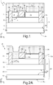
- a transistor of this type is illustrated schematically in Figure 1 .
- Figure 1 shows, in a triaxial system of mutually orthogonal axes X, Y, Z, a HEMT device 1, which includes: a substrate 2, made, for example, of silicon; a channel layer 4 of intrinsic gallium nitride (GaN), which extends over the substrate 2; a barrier layer 6 of intrinsic aluminium and gallium nitride (AlGaN), which extends over the channel layer 4; an insulation layer 7 of dielectric material, such as nickel oxide (NiO), which extends on an upper side 6a of the barrier layer 6; and a gate region 8, which extends in the insulation layer 7 between a source terminal 10 and a drain terminal 12.
- a HEMT device 1 which includes: a substrate 2, made, for example, of silicon; a channel layer 4 of intrinsic gallium nitride (GaN), which extends over the substrate 2; a barrier layer 6 of intrinsic aluminium and gallium nitride (AlGaN), which extends over the channel layer 4; an insulation
- the channel layer 4 and the barrier layer 6 form a heterostructure 3.
- a buffer layer may be present between the substrate 2 and the heterostructure 3.
- a gate terminal 8, of a recessed type extends in depth through the insulation layer 7, until it reaches the barrier layer 6.
- the gate terminal 8 is formed in a trench 9 dug through the insulation layer 7.
- the source terminal 10 and the drain terminal 12, which are made of conductive material, for example metal material, extend in depth in the semiconductor body 5, completely through the barrier layer 6, terminating at the interface between the barrier layer 6 and the channel layer 4.
- the channel layer 4 and the barrier layer 6 are, in general, made of materials such that, when they are coupled together as illustrated in Figure 1 , they form a heterojunction that enables formation of a region, or layer, of two-dimensional gas (2DEG).
- a gate dielectric layer 8a extends in the trench 9, facing the bottom and side walls of the trench 9.
- a gate metallization 8b completes filling of the trench 9 and extends over the gate dielectric layer 8a.
- the gate dielectric layer 8a and the gate metallization 8b form the gate region of the HEMT device 1.
- the gate terminal 8 is separated laterally (i.e., along X) from the source terminal 10 and drain terminal 12 by means of respective portions 7a and 7b of the insulation layer 7.
- the gate metallization 8b likewise extends over the insulation layer 7, alongside the trench 9, forming in particular a field-plate element 8c that extends along X towards the source terminal 10.
- a similar field-plate element 8d extends along X in the opposite direction, i.e., towards the drain terminal 12.
- a passivation layer 5 for example made of insulating or dielectric material, in particular silicon nitride (Si 3 N 4 ), extends over the source terminal 10, the drain terminal 12, and the gate terminal 8, and over the insulation layer 7.
- the passivation layer 5 has the function of protection of the source terminal 10, the drain terminal 12, and the gate terminal 8 from external agents.
- the field-plate gate topology is an efficient technique used for reducing the high electrical field in the region between the gate terminal and the drain terminal.
- the field-plate gate topology implies a design of the HEMT device 1 such that the side of the gate terminal 8 facing the drain terminal 12 extends over the insulation layer 7 to form the field-plate element 8d, so as to reduce the electrical field in the region between the gate terminal 8 and the drain terminal 12 and thus raise the breakdown threshold of the HEMT device 1.
- the distance L D between the gate terminal 8 and the source terminal 10 is a parameter that significantly affects the value of the current density supplied at output from the HEMT device 1, the value of ON-state resistance R ON , and the peak value of the transconductance, in particular for radiofrequency (RF) applications and low-voltage power applications.
- the aforementioned parameters improve by approaching the gate terminal 8 to the source terminal 10, i.e., reducing the distance L D between the gate terminal 8 and the source terminal 10, measured along the axis X at the top surface 6a of the channel layer 6.
- the RF gain is proportional to the ratio between the cut-off frequency F t and the value of frequency f (RF gain ⁇ F t/ f), where Ft is proportional to the inverse of the capacitance C GS between the gate terminal 8 and the source terminal 10 (F t ⁇ 1/C GS ). Consequently, to maximise the RF gain, it is expedient to reduce the value of the capacitance C GS , or, in other words, to move the field-plate element 8c away from the source terminal 10. Moreover, it may be noted that also the capacitance that is formed between the field-plate element 8c and the underlying heterostructure 3 has a negative impact on the RF gain.
- Patent document JP2009267155 provides a semiconductor device which modulate a carrier density and electric field in a carrier moving direction in a two-dimensional carrier gas channel generated, in a nitride-based semiconductor functional layer.
- Patent document US2014/284613 describes a nitride-based semiconductor device and a method of manufacturing the same.
- Patent document US2017/077284 describes a semiconductor device having high breakdown voltage property.
- HEMT transistor and a method for manufacturing the transistor are provided, as defined in the annexed claims.
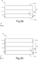
- Figure 2A shows a HEMT device 31, in a triaxial system of mutually orthogonal axes X, Y, Z.
- the present invention applies indifferently to a HEMT device of a normally-off type or of a normally-on type.
- the HEMT device 31 includes a substrate 12, made, for example, of silicon, or silicon carbide (SiC), or sapphire (Al 2 O 3 ); an (optional) buffer layer 22, which extends on the substrate 12; a channel layer 14 made of intrinsic gallium nitride (GaN), which extends on the buffer layer 22 (or directly on the substrate 12 in the case where the buffer layer 22 is not present), and has a thickness comprised between approximately 1 ⁇ m and 5 ⁇ m; a barrier layer 16, made of intrinsic aluminium and gallium nitride (AlGaN) or, more in general, of compounds based upon ternary or quaternary alloys of gallium nitride, such as Al x Ga 1-x N, AlInGaN, In x Ga 1-x N, and Al x In 1-x Al, which extends on the channel layer 14 and has a thickness t b comprised between approximately 5 nm and 30 nm; an insulation layer 17, made of dielectric material, such as nickel
- the channel layer 14 and the barrier layer 16 form a heterostructure 13.
- the substrate 12, the buffer layer 22 (when present), the channel layer 14, and the barrier layer 16 are hereinafter referred to, as a whole, as “semiconductor body 20".
- the heterostructure 13 hence extends between an underside 14a of the channel layer 14, which constitutes part of the interface with the underlying substrate 12, and an upper side 16a of the barrier layer 16.
- the channel layer 14 and the barrier layer 16 are, in general, made of materials such that, when coupled together, as illustrated in Figure 2A , form a heterojunction that enables formation of a region, or layer, of two-dimensional gas (2DEG).
- the gate terminal 18, which comprises a gate dielectric 18a and a gate metallization 18b, extends throughout the thickness of the insulation layer 17, until it reaches the barrier layer 16.
- the gate terminal 18 extends through a part of the barrier layer 16 and terminates within the barrier layer 16.
- the gate dielectric layer 18a electrically insulates the gate metallization 18b from the barrier layer 16.
- the 2DEG region extends at the interface between the channel layer 14 and the barrier layer 16 underneath the insulation layer 17, i.e., in interface portions between the channel layer 14 and the barrier layer 16 corresponding to the projection along Z of the insulation layer 17.
- the semiconductor body 20 may comprise, according to the need, just one or more than one layer of GaN, or GaN alloys, appropriately doped or of an intrinsic type.
- the gate terminal 18 is separated laterally (i.e., along X) from the drain terminal 22 by means of a portion 17' of the insulation layer 17.
- a respective portion of the insulation layer 17 is not, instead, present between the gate terminal 18 and the source terminal 21.
- a minimum distance L GS ' between the gate terminal 18 and the source terminal 21, measured along X, is equal to a distance L D ' between the gate terminal 18 and the source terminal 21 measured at the surface 16a of the barrier layer 16.
- L D the distance between the gate terminal 18 and the source terminal 21 remains constant throughout the extension, along Z, of the side surface 25 of the gate terminal 18 that faces the source terminal 21.
- this side surface 25 extends, or lies, in the plane YZ and has, in each point considered, the same distance L D from the source terminal 21.
- the distance L D is measured, in each point considered of the side surface, in a direction parallel to the axis X, which is orthogonal to the plane YZ.
- the distance L D is considered constant even in the presence of non-idealities deriving from the manufacturing process, for example corrugations, depressions, or protuberances present on the side surface 25 of the gate terminal 18 and/or on the facing surface of the source terminal 21.
- the distance between the gate terminal 18 and the source terminal 21 is chosen, in the design step, so as to improve at the same time the value of ON-state resistance R ON and the peak value of the transconductance, and to maximise the RF gain.
- the present invention makes it possible to approach the gate terminal 18 to the source terminal 21 with a reduction of the risk of shorting (owing to the absence of the corresponding field-plate element) and at the same time to maximise the RF gain when the contribution of capacitance between the field-plate element facing the source terminal and the underlying heterostructure is eliminated.
- the side extension, along X, of the HEMT device 31 can be reduced, for example by a value equal to the extension along X of the field-plate element 8c, which is now no longer present.
- the present invention by eliminating the field-plate element exclusively in the spatial region between the gate terminal and the source terminal, it is possible to obtain a HEMT transistor configured to meet as well as possible specific needs of application, reducing the design constraints.
- the passivation layer 24 extends between the gate terminal 18 and the source terminal 21 until it reaches and physically contacts the channel layer 16.
- the passivation layer 24 has the function of protection of the source terminal 21, the drain terminal 22, and the gate terminal 18 from external agents and likewise has the function of side electrical insulation between the gate terminal 18 and the source terminal 21.
- a further field-plate metal layer 26, illustrated in Figure 2B extends over the passivation layer 24, in particular on the gate terminal 18 and likewise alongside the latter.
- a dielectric layer 27, for example made of SiO 2 is, in this case, present.
- the remaining elements of Figure 2B correspond to the ones already illustrated in Figure 2A and described with reference to Figure 2A . They are not hence described any further, and they are identified by the same reference numbers.
- Figure 3A shows, in cross-sectional view, a portion of a wafer 40 during a step for manufacturing the HEMT device 31, according to an embodiment of the present invention. Elements of the wafer 40 common to the ones already described above with reference to Figure 2 , and illustrated in Figure 2 , are designated by the same reference numbers.
- the wafer 40 is provided, comprising: the substrate 12, made, for example, of silicon (Si) or silicon carbide (SiC) or aluminium oxide (Al 2 O 3 ), having a front side 12a and a back side 12b opposite to one another in a direction Z; the channel layer 14, made of gallium nitride (GaN), having its own underside 14a that extends adjacent to and overlapping the front side 12a of the substrate 12; and the barrier layer 16, made of gallium and aluminium nitride (AlGaN), which extends over the channel layer 14.
- the barrier layer 16 and the channel layer 14 form the heterostructure 13.
- the insulation layer 17 formed on a front side 16a of the barrier layer 16 is the insulation layer 17, made of dielectric material such as silicon oxide (SiO 2 ) and having a thickness comprised between 10 nm and 150 nm.
- the insulation layer 17 may also be made of nickel oxide (NiO), or silicon nitride (Si 3 N 4 ), or aluminium oxide (Al 2 O 3 ), or aluminium nitride (AlN). Formation of the insulation layer 17 is performed via epitaxial growth on the barrier layer 6 (AlGaN).
- AlGaN barrier layer 6
- MOCVD Metal Organic Chemical Vapour Deposition
- a step of masked etching of the insulation layer 17 is carried out to remove selective portions of the latter that extend in regions of the wafer 40 in which it is desired to form the source region 21 and the drain region 22 of the HEMT device 1.
- Etching proceeds, possibly with a different etching chemistry, for removing exposed portions of the barrier layer 16, until the channel layer 14 is reached.
- openings 34a and 34b are formed.
- a step of formation of ohmic contacts is carried out to obtain the source and drain regions 21, 22 by depositing conductive material, in particular a metal, such as titanium (Ti), tantalum (Ta), aluminium (Al), or alloys or compounds thereof, by means of sputtering or vapour deposition, within the openings 34a, 34b.
- conductive material in particular a metal, such as titanium (Ti), tantalum (Ta), aluminium (Al), or alloys or compounds thereof, by means of sputtering or vapour deposition, within the openings 34a, 34b.
- RTA rapid thermal annealing
- the insulation layer 17 is selectively removed, for example by means of lithographic and etching steps so as to remove selective portions thereof in a region of the wafer 40 in which, in subsequent steps, the gate region 18 of the HEMT device 31 is to be formed.
- the etching step can stop at the underlying barrier layer 16 (as illustrated in Figure 3E ), or else proceed partially within the barrier layer 16 or, again, completely involve the barrier layer 16 (in a way not illustrated in the figures).
- a surface portion 16' of the barrier layer 16 is thus exposed.
- Etching of the barrier layer 16 is, for example, of a dry type.
- the portion of the barrier layer 16 removed generates a trench 19, which extends throughout the thickness of the insulation layer 17.
- the step of Figure 3E envisages etching of the insulation layer 17 in a region that extends from the source terminal 21 towards the drain terminal 22 (without reaching the latter), with removal of the insulation layer 17 alongside the source terminal 21.
- the gate dielectric layer 18a formed, for instance by deposition, is the gate dielectric layer 18a, made for example of a material chosen from among aluminium nitride (AlN), silicon nitride (SiN), aluminium oxide (Al 2 O 3 ), and silicon oxide (SiO 2 ).
- the gate dielectric layer 18a has a thickness chosen between 5 nm and 50 nm, for example 30 nm.
- the gate metallization 18b is made of metal material, such as tantalum (Ta), tantalum nitride (TaN), titanium nitride (TiN), palladium (Pa), tungsten (W), tungsten silicide (WSi 2 ), titanium aluminium (Ti/Al), and nickel gold (Ni/Au).
- metal material such as tantalum (Ta), tantalum nitride (TaN), titanium nitride (TiN), palladium (Pa), tungsten (W), tungsten silicide (WSi 2 ), titanium aluminium (Ti/Al), and nickel gold (Ni/Au).
- the gate dielectric layer 18a that is not protected by the gate metallization 18b (and in particular the portion of the gate dielectric 18a that extends, in top plan view in the plane XY, between the gate metallization 18b and the source terminal 21), can be removed by means of an etching step or kept on the wafer 40, indifferently.
- Formation of the gate terminal 18 does not damage the source and drain terminals already formed. In fact, even though some of the metals of the source and drain terminals (typically, Ti and Ta) could be partially etched, the effect thereon is not important for operation of the device; the aluminium is not damaged, nor partially etched, by the chemistry used for etching the gate dielectric 18a.
- the metals of the source and drain terminals typically, Ti and Ta
- the gate terminal 18 is formed, as mentioned previously with reference to Figure 2A , so as to provide the gate metallization 18b at a distance L D from the source terminal 21.
- Just one field-plate element 18' extends as a continuation of the gate metallization 18b towards the drain terminal 22, on the insulation layer 17.
- No similar field-plate element is instead present extending towards the source terminal 21 in so far as, in the spatial region between the gate terminal 18 and the source terminal 21, the insulation layer 17 is absent.
- a step of deposition of the passivation layer 24 is carried out. This step is performed, for example, by depositing a layer of 400 nm by means of PECVD.
- the material of the passivation layer 24 is deposited within the space present between the gate terminal 18 and the source terminal 21, filling it and electrically insulating the gate terminal 18 from the source terminal 21.
- the HEMT device 31 illustrated in Figure 2A is thus formed.
- the metallization of the (source, drain, and gate) contacts on the front of the wafer can be performed using any variant known in the literature, such as formation of contacts made of AlSiCu/Ti or Al/Ti, or W-plugs, or others still.
- the channel layer 4 and the barrier layer 6 may be made of other materials chosen from among compound materials constituted by elements of Groups III and V, such as InGaN/GaN or AIN/GaN.
Landscapes
- Junction Field-Effect Transistors (AREA)
- Engineering & Computer Science (AREA)
- Manufacturing & Machinery (AREA)
Abstract
Description
- The present invention relates to a HEMT (High-Electron-Mobility Transistor) and to the manufacturing method thereof. In particular, the present invention regards a HEMT transistor with adjusted gate-source distance.
- Transistor are known, which are based upon the formation of layers of two-dimensional electron gas (2DEG) with high mobility at a heterojunction, i.e., at the interface between semiconductor materials with different band gaps. For instance, HEMT transistors are known based upon the heterojunction between a layer of aluminium and gallium nitride (AlGaN) and a layer of gallium nitride (GaN).
- HEMT transistors based upon AlGaN/GaN heterojunctions afford a wide range of advantages that render them particularly suited and widely used for various applications. For instance, the high breakdown threshold of HEMT transistors is exploited for high-performance power switches. The high mobility of the electrons in the conductive channel makes it possible to provide high-frequency amplifiers. Moreover, the high concentration of electrons in the 2DEG enables a low ON-state resistance (RON) to be obtained.
- On account of the high cost of gallium-nitride substrates, HEMT transistors based upon AlGaN/GaN heterojunctions are normally obtained via growth of GaN and AlGaN layers on silicon substrates. Consequently, the HEMT transistors thus obtained are of a planar type; i.e., they have the source, gate, and drain electrodes or terminals aligned in a plane parallel to the substrate.
- A known solution for providing HEMT transistors consists in the use of recessed-gate terminals.
- A transistor of this type is illustrated schematically in
Figure 1 . -
Figure 1 shows, in a triaxial system of mutually orthogonal axes X, Y, Z, aHEMT device 1, which includes: asubstrate 2, made, for example, of silicon; achannel layer 4 of intrinsic gallium nitride (GaN), which extends over thesubstrate 2; a barrier layer 6 of intrinsic aluminium and gallium nitride (AlGaN), which extends over thechannel layer 4; aninsulation layer 7 of dielectric material, such as nickel oxide (NiO), which extends on anupper side 6a of the barrier layer 6; and agate region 8, which extends in theinsulation layer 7 between asource terminal 10 and adrain terminal 12. - The
channel layer 4 and the barrier layer 6 form aheterostructure 3. - In a way not illustrated in the figure, a buffer layer may be present between the
substrate 2 and theheterostructure 3. - A
gate terminal 8, of a recessed type, extends in depth through theinsulation layer 7, until it reaches the barrier layer 6. In other words, thegate terminal 8 is formed in atrench 9 dug through theinsulation layer 7. Thesource terminal 10 and thedrain terminal 12, which are made of conductive material, for example metal material, extend in depth in thesemiconductor body 5, completely through the barrier layer 6, terminating at the interface between the barrier layer 6 and thechannel layer 4. Thechannel layer 4 and the barrier layer 6 are, in general, made of materials such that, when they are coupled together as illustrated inFigure 1 , they form a heterojunction that enables formation of a region, or layer, of two-dimensional gas (2DEG). - A gate
dielectric layer 8a extends in thetrench 9, facing the bottom and side walls of thetrench 9. Agate metallization 8b completes filling of thetrench 9 and extends over the gatedielectric layer 8a. The gatedielectric layer 8a and thegate metallization 8b form the gate region of theHEMT device 1. - The
gate terminal 8 is separated laterally (i.e., along X) from thesource terminal 10 anddrain terminal 12 by means ofrespective portions insulation layer 7. As illustrated inFigure 1 , as a consequence of the manufacturing process currently used, thegate metallization 8b likewise extends over theinsulation layer 7, alongside thetrench 9, forming in particular a field-plate element 8c that extends along X towards thesource terminal 10. A similar field-plate element 8d extends along X in the opposite direction, i.e., towards thedrain terminal 12. - A
passivation layer 5, for example made of insulating or dielectric material, in particular silicon nitride (Si3N4), extends over thesource terminal 10, thedrain terminal 12, and thegate terminal 8, and over theinsulation layer 7. Thepassivation layer 5 has the function of protection of thesource terminal 10, thedrain terminal 12, and thegate terminal 8 from external agents. - The field-plate gate topology is an efficient technique used for reducing the high electrical field in the region between the gate terminal and the drain terminal. The field-plate gate topology implies a design of the
HEMT device 1 such that the side of thegate terminal 8 facing thedrain terminal 12 extends over theinsulation layer 7 to form the field-plate element 8d, so as to reduce the electrical field in the region between thegate terminal 8 and thedrain terminal 12 and thus raise the breakdown threshold of theHEMT device 1. - In current manufacturing processes, formation of the field-plate element 8d, oriented towards the
drain terminal 12, is obtained simultaneously with formation of the field-plate element 8c, oriented towards thesource terminal 10. - The present applicant has found that, even though AlGaN/GaN structures form a 2DEG layer with low electrical resistance thanks to the high current density and electron mobility, the distance LD between the
gate terminal 8 and thesource terminal 10 is a parameter that significantly affects the value of the current density supplied at output from theHEMT device 1, the value of ON-state resistance RON, and the peak value of the transconductance, in particular for radiofrequency (RF) applications and low-voltage power applications. - In particular, the aforementioned parameters improve by approaching the
gate terminal 8 to thesource terminal 10, i.e., reducing the distance LD between thegate terminal 8 and thesource terminal 10, measured along the axis X at thetop surface 6a of the channel layer 6. - However, a reduction of the distance LD causes an undesired approach of the field-plate element 8c to the
source terminal 10. This aspect is undesired in so far as it increases the risk of short-circuits between thegate terminal 8 and thesource terminal 10 and likewise increases the value of capacitance CGS between thegate terminal 8 and thesource terminal 10. - Moreover, it should be noted that the RF gain, RFgain, is proportional to the ratio between the cut-off frequency Ft and the value of frequency f (RFgain ≈ Ft/f), where Ft is proportional to the inverse of the capacitance CGS between the
gate terminal 8 and the source terminal 10 (Ft ≈ 1/CGS). Consequently, to maximise the RF gain, it is expedient to reduce the value of the capacitance CGS, or, in other words, to move the field-plate element 8c away from thesource terminal 10. Moreover, it may be noted that also the capacitance that is formed between the field-plate element 8c and theunderlying heterostructure 3 has a negative impact on the RF gain. - It is hence evident that a compromise solution must be sought in order to optimise the aforementioned parameters.
- Patent document
JP2009267155 - Patent document
US2014/284613 describes a nitride-based semiconductor device and a method of manufacturing the same. - Patent document
US2017/077284 describes a semiconductor device having high breakdown voltage property. - However, the above-mentioned issues remain unsolved.
- There is consequently felt the need to provide a HEMT, and a manufacturing method thereof, that will take into due consideration the contrasting requisites set forth previously.
- Hence, according to the present invention a HEMT transistor and a method for manufacturing the transistor are provided, as defined in the annexed claims.
- For a better understanding of the present invention, preferred embodiments thereof are now described, purely by way of non-limiting example, with reference to the attached drawings, wherein:
-
Figure 1 is a side section view of a HEMT transistor according to an embodiment of a known type; -
Figure 2A is a side section view of a HEMT transistor according to an embodiment of the present invention; -
Figure 2B is a side section view of a HEMT transistor according to a further embodiment of the present invention; and -
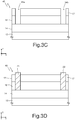
Figures 3A-3F show steps for manufacturing the HEMT transistor ofFigure 2A . -
Figure 2A shows aHEMT device 31, in a triaxial system of mutually orthogonal axes X, Y, Z. The present invention applies indifferently to a HEMT device of a normally-off type or of a normally-on type. - The HEMT
device 31 includes asubstrate 12, made, for example, of silicon, or silicon carbide (SiC), or sapphire (Al2O3); an (optional)buffer layer 22, which extends on thesubstrate 12; achannel layer 14 made of intrinsic gallium nitride (GaN), which extends on the buffer layer 22 (or directly on thesubstrate 12 in the case where thebuffer layer 22 is not present), and has a thickness comprised between approximately 1 µm and 5 µm; abarrier layer 16, made of intrinsic aluminium and gallium nitride (AlGaN) or, more in general, of compounds based upon ternary or quaternary alloys of gallium nitride, such as AlxGa1-xN, AlInGaN, InxGa1-xN, and AlxIn1-xAl, which extends on thechannel layer 14 and has a thickness tb comprised between approximately 5 nm and 30 nm; aninsulation layer 17, made of dielectric material, such as nickel oxide (NiO), which extends on anupper side 16a of thebarrier layer 16; and agate terminal 18, which extends in theinsulation layer 7 between asource terminal 21 and adrain terminal 22. - The
channel layer 14 and thebarrier layer 16 form aheterostructure 13. Thesubstrate 12, the buffer layer 22 (when present), thechannel layer 14, and thebarrier layer 16 are hereinafter referred to, as a whole, as "semiconductor body 20". Theheterostructure 13 hence extends between anunderside 14a of thechannel layer 14, which constitutes part of the interface with theunderlying substrate 12, and anupper side 16a of thebarrier layer 16. Thechannel layer 14 and thebarrier layer 16 are, in general, made of materials such that, when coupled together, as illustrated inFigure 2A , form a heterojunction that enables formation of a region, or layer, of two-dimensional gas (2DEG). - The
gate terminal 18, which comprises a gate dielectric 18a and agate metallization 18b, extends throughout the thickness of theinsulation layer 17, until it reaches thebarrier layer 16. Optionally, according to a different embodiment (not illustrated), thegate terminal 18 extends through a part of thebarrier layer 16 and terminates within thebarrier layer 16. The gatedielectric layer 18a electrically insulates thegate metallization 18b from thebarrier layer 16. - The
source region 21 and thedrain region 22, which are made of conductive material, for example metal, extend in depth in thesemiconductor body 20, right through thebarrier layer 16, terminating at the interface between thebarrier layer 16 and thechannel layer 14. - The 2DEG region extends at the interface between the
channel layer 14 and thebarrier layer 16 underneath theinsulation layer 17, i.e., in interface portions between thechannel layer 14 and thebarrier layer 16 corresponding to the projection along Z of theinsulation layer 17. According to further embodiments, thesemiconductor body 20 may comprise, according to the need, just one or more than one layer of GaN, or GaN alloys, appropriately doped or of an intrinsic type. - According to an aspect of the present invention, the
gate terminal 18 is separated laterally (i.e., along X) from thedrain terminal 22 by means of a portion 17' of theinsulation layer 17. A respective portion of theinsulation layer 17 is not, instead, present between thegate terminal 18 and thesource terminal 21. In this way, during the manufacturing steps, as illustrated more fully hereinafter, there is no formation of a field-plate element, of the type designated by the reference 8c inFigure 1 , which protrudes towards thesource terminal 21. - A minimum distance LGS' between the
gate terminal 18 and thesource terminal 21, measured along X, is equal to a distance LD' between thegate terminal 18 and thesource terminal 21 measured at thesurface 16a of thebarrier layer 16. Given the absence of the field-plate element between thegate terminal 18 and thesource terminal 21, the distance between thegate terminal 18 and thesource terminal 21 remains constant throughout the extension, along Z, of theside surface 25 of thegate terminal 18 that faces thesource terminal 21. In other words, thisside surface 25 extends, or lies, in the plane YZ and has, in each point considered, the same distance LD from thesource terminal 21. The distance LD is measured, in each point considered of the side surface, in a direction parallel to the axis X, which is orthogonal to the plane YZ. It is evident that the distance LD is considered constant even in the presence of non-idealities deriving from the manufacturing process, for example corrugations, depressions, or protuberances present on theside surface 25 of thegate terminal 18 and/or on the facing surface of thesource terminal 21. - According to the present invention, the distance between the
gate terminal 18 and thesource terminal 21 is chosen, in the design step, so as to improve at the same time the value of ON-state resistance RON and the peak value of the transconductance, and to maximise the RF gain. - In fact, as compared to the embodiment of a known type represented in
Figure 1 , the present invention makes it possible to approach thegate terminal 18 to thesource terminal 21 with a reduction of the risk of shorting (owing to the absence of the corresponding field-plate element) and at the same time to maximise the RF gain when the contribution of capacitance between the field-plate element facing the source terminal and the underlying heterostructure is eliminated. - Moreover, the side extension, along X, of the
HEMT device 31 can be reduced, for example by a value equal to the extension along X of the field-plate element 8c, which is now no longer present. - In other words, according to the present invention, by eliminating the field-plate element exclusively in the spatial region between the gate terminal and the source terminal, it is possible to obtain a HEMT transistor configured to meet as well as possible specific needs of application, reducing the design constraints.
- A
passivation layer 24, made, for example, of insulating or dielectric material such as Si3N4, SiO2, Al2O3, or AlN, extends on thesource terminal 21, thedrain terminal 22, and thegate terminal 18, and in particular between thegate terminal 18 and thesource terminal 21. Thepassivation layer 24 extends between thegate terminal 18 and thesource terminal 21 until it reaches and physically contacts thechannel layer 16. - The
passivation layer 24 has the function of protection of thesource terminal 21, thedrain terminal 22, and thegate terminal 18 from external agents and likewise has the function of side electrical insulation between thegate terminal 18 and thesource terminal 21. - According to another embodiment, a further field-
plate metal layer 26, illustrated inFigure 2B , extends over thepassivation layer 24, in particular on thegate terminal 18 and likewise alongside the latter. To provide protection and insulation of the above further field-plate metal layer 26, adielectric layer 27, for example made of SiO2, is, in this case, present. The remaining elements ofFigure 2B correspond to the ones already illustrated inFigure 2A and described with reference toFigure 2A . They are not hence described any further, and they are identified by the same reference numbers. - Illustrated in what follows, with reference to
Figures 3A-3F , are steps for manufacturing theHEMT device 1.Figure 3A shows, in cross-sectional view, a portion of awafer 40 during a step for manufacturing theHEMT device 31, according to an embodiment of the present invention. Elements of thewafer 40 common to the ones already described above with reference toFigure 2 , and illustrated inFigure 2 , are designated by the same reference numbers. In particular (Figure 3A ), thewafer 40 is provided, comprising: thesubstrate 12, made, for example, of silicon (Si) or silicon carbide (SiC) or aluminium oxide (Al2O3), having afront side 12a and aback side 12b opposite to one another in a direction Z; thechannel layer 14, made of gallium nitride (GaN), having itsown underside 14a that extends adjacent to and overlapping thefront side 12a of thesubstrate 12; and thebarrier layer 16, made of gallium and aluminium nitride (AlGaN), which extends over thechannel layer 14. Thebarrier layer 16 and thechannel layer 14 form theheterostructure 13. - Next (
Figure 3B ), formed on afront side 16a of thebarrier layer 16 is theinsulation layer 17, made of dielectric material such as silicon oxide (SiO2) and having a thickness comprised between 10 nm and 150 nm. Theinsulation layer 17 may also be made of nickel oxide (NiO), or silicon nitride (Si3N4), or aluminium oxide (Al2O3), or aluminium nitride (AlN). Formation of theinsulation layer 17 is performed via epitaxial growth on the barrier layer 6 (AlGaN). With reference to Roccaforte, F. et al., "Epitaxial NiO gate dielectric on AlGaN/GaN heterostructures", Appl. Phys. Lett., vol. 100, 063511, 2012, it is known that it is possible to carry out an epitaxial growth of NiO on AlGaN by means of MOCVD (Metal Organic Chemical Vapour Deposition). - Then (
Figure 3C ), a step of masked etching of theinsulation layer 17 is carried out to remove selective portions of the latter that extend in regions of thewafer 40 in which it is desired to form thesource region 21 and thedrain region 22 of theHEMT device 1. Etching proceeds, possibly with a different etching chemistry, for removing exposed portions of thebarrier layer 16, until thechannel layer 14 is reached. In particular,openings - Then (
Figure 3D ), a step of formation of ohmic contacts is carried out to obtain the source and drainregions openings - This is followed by a step of rapid thermal annealing (RTA), for example at a temperature of between approximately 500°C and 700°C for a time of from 30 s to 120 s, which makes it possible to perfect formation of the ohmic contacts of the
source region 21 and thedrain region 22 with the underlying region (presenting the 2DEG). - Then (
Figure 3E ), theinsulation layer 17 is selectively removed, for example by means of lithographic and etching steps so as to remove selective portions thereof in a region of thewafer 40 in which, in subsequent steps, thegate region 18 of theHEMT device 31 is to be formed. - The etching step can stop at the underlying barrier layer 16 (as illustrated in
Figure 3E ), or else proceed partially within thebarrier layer 16 or, again, completely involve the barrier layer 16 (in a way not illustrated in the figures). - A surface portion 16' of the
barrier layer 16 is thus exposed. Etching of thebarrier layer 16 is, for example, of a dry type. The portion of thebarrier layer 16 removed generates atrench 19, which extends throughout the thickness of theinsulation layer 17. - As described with reference to
Figure 2A , the step ofFigure 3E envisages etching of theinsulation layer 17 in a region that extends from thesource terminal 21 towards the drain terminal 22 (without reaching the latter), with removal of theinsulation layer 17 alongside thesource terminal 21. - Then (
Figure 3F ), formed, for instance by deposition, is thegate dielectric layer 18a, made for example of a material chosen from among aluminium nitride (AlN), silicon nitride (SiN), aluminium oxide (Al2O3), and silicon oxide (SiO2). Thegate dielectric layer 18a has a thickness chosen between 5 nm and 50 nm, for example 30 nm. - Then, a step of deposition of conductive material on the
wafer 40 is carried out to form, by means of known photolithographic techniques, thegate metallization 18b on thegate dielectric layer 18a, filling thetrench 19 and thus forming thegate region 18. For instance, thegate metallization 18b is made of metal material, such as tantalum (Ta), tantalum nitride (TaN), titanium nitride (TiN), palladium (Pa), tungsten (W), tungsten silicide (WSi2), titanium aluminium (Ti/Al), and nickel gold (Ni/Au). - The
gate dielectric layer 18a that is not protected by thegate metallization 18b (and in particular the portion of thegate dielectric 18a that extends, in top plan view in the plane XY, between thegate metallization 18b and the source terminal 21), can be removed by means of an etching step or kept on thewafer 40, indifferently. - Formation of the
gate terminal 18 does not damage the source and drain terminals already formed. In fact, even though some of the metals of the source and drain terminals (typically, Ti and Ta) could be partially etched, the effect thereon is not important for operation of the device; the aluminium is not damaged, nor partially etched, by the chemistry used for etching thegate dielectric 18a. - The
gate terminal 18 is formed, as mentioned previously with reference toFigure 2A , so as to provide thegate metallization 18b at a distance LD from thesource terminal 21. Just one field-plate element 18' extends as a continuation of thegate metallization 18b towards thedrain terminal 22, on theinsulation layer 17. No similar field-plate element is instead present extending towards thesource terminal 21 in so far as, in the spatial region between thegate terminal 18 and thesource terminal 21, theinsulation layer 17 is absent. - Finally, a step of deposition of the
passivation layer 24 is carried out. This step is performed, for example, by depositing a layer of 400 nm by means of PECVD. - The material of the
passivation layer 24 is deposited within the space present between thegate terminal 18 and thesource terminal 21, filling it and electrically insulating thegate terminal 18 from thesource terminal 21. - The
HEMT device 31 illustrated inFigure 2A is thus formed. - The advantages of the invention according to the present disclosure emerge clearly from what has been set forth previously.
- In particular, there may be noted, according to the present invention, a reduction in the RON (due to a shorter gate-source distance), and hence an increase in the maximum current supplied at output from the device and also in the output power.
- Moreover, there may be noted a reduction in the gate-to-source capacitance CGS and hence an increase in the cut-off frequency and gain, in particular in RF applications.
- Finally, it is clear that modifications and variations may be made to what has been described and illustrated herein, without thereby departing from the sphere of protection of the present invention, as defined in the annexed claims.
- For instance, the metallization of the (source, drain, and gate) contacts on the front of the wafer can be performed using any variant known in the literature, such as formation of contacts made of AlSiCu/Ti or Al/Ti, or W-plugs, or others still.
- Moreover, the
channel layer 4 and the barrier layer 6 may be made of other materials chosen from among compound materials constituted by elements of Groups III and V, such as InGaN/GaN or AIN/GaN.
Claims (14)
- A method for manufacturing a HEMT transistor (31), comprising the steps of:- forming a heterostructure (13);- forming a dielectric layer (17) on the heterostructure (13);- forming a source electrode (21) and a drain electrode (22) through the dielectric layer (17) electrically contacting said heterostructure; and- forming a gate electrode (18), between the source electrode (21) and the drain electrode (22),the method being characterized in that the step of forming the gate electrode (18) comprises:- removing selective portions of the dielectric layer (17) adjacent to the source electrode (21) to form a trench (19) throughout the entire thickness of the dielectric layer (17); and- depositing conductive material in said trench (19) and shaping said conductive material so as to form a gate metallization (18b) having a side surface (25), facing the source electrode (21), which extends at a distance (LD) from the source electrode (21) that is constant throughout the entire extension of said gate metallization (18b).
- The method according to Claim 1, wherein said distance (LD) is taken along a first direction (X) orthogonal to a plane (YZ) defined by said side surface (25) of the gate metallization (18b).
- The method according to Claim 2, wherein the step of shaping said conductive material includes etching the conductive material along a second direction (Z) orthogonal to said first direction (X).
- The method according to any one of the preceding claims, wherein the step of removing selective portions of the dielectric layer (17) comprises removing completely the dielectric layer (17) between the gate electrode (18) to be formed and the source electrode (21) and maintaining the dielectric layer (17) between the gate electrode (18) to be formed and the drain electrode (22).
- The method according to any one of the preceding claims, further comprising the step of forming a passivation layer (24) in said trench (19) after the step of forming the gate electrode (18) thus completing a filling of the trench (19),
the passivation layer (24) being further formed over the source electrode (21), and the drain electrode (22). - The method according to any one of the preceding claims, wherein the step of shaping said conductive material further comprises the step of forming, simultaneously with the gate metallization (18b), a field-plate element (18') that extends over the dielectric layer (17) starting from the gate metallization (18b) towards the drain electrode (22).
- The method according to any one of the preceding claims, wherein the step of forming the gate electrode (18) further comprises, prior to the step of depositing conductive material in the trench (19), the step of forming a gate dielectric layer (18a) in the trench (19), and wherein the step of depositing conductive material in the trench (19) comprises depositing said conductive material on the layer of dielectric material (18a).
- A HEMT transistor (31) comprising:- a heterostructure (13);- a dielectric layer (17) on the heterostructure (13);- a source electrode (21) and a drain electrode (22), which extend in electrical contact with the heterostructure (13); and- a gate electrode (18), which extends between the source electrode (21) and the drain electrode (22),characterized in that the gate electrode (18) includes a gate metallization (18b) having a side surface (25), facing the source electrode (21), which extends at a distance (LD) from the source electrode (21) that is constant throughout the entire extension of said gate metallization (18b).
- The HEMT transistor according to Claim 8, wherein said distance (LD) is taken along a first direction (X) orthogonal to a plane (YZ) defined by said side surface (25) of the gate metallization (18b).
- The HEMT transistor according to Claim 8 or Claim 9, further comprising a passivation layer (24) that extends between the gate electrode (18) and the source electrode (21) throughout the entire extension of said side surface (25), and likewise over the gate electrode (18), the source electrode (21), and the drain electrode (22).
- The HEMT transistor according to Claim 10, wherein the heterostructure (13) includes a channel layer (14) and a barrier layer (16) on the channel layer (14), and said passivation layer (24) extends between the gate electrode (18) and the source electrode (21) until it reaches the barrier layer (16).
- The HEMT transistor according to Claim 10, wherein the heterostructure (13) includes a channel layer (14) and a barrier layer (16) on the channel layer (14), and the gate electrode (18) comprises a gate dielectric layer (18a) and a gate metallization (18b), said gate dielectric layer (18a) extending in contact with the barrier layer (16) between the gate metallization (18b) and the barrier layer (16), and laterally with respect to the gate metallization (18b) between the gate electrode (18) and the source electrode (21),
and wherein said passivation layer (24) extends between the gate electrode (18) and the source electrode (21) until it reaches the gate dielectric layer (18a). - The HEMT transistor according to any one of the Claims 8 to 12, wherein the dielectric layer (17) extends between the gate electrode (18) and the drain electrode (22) and is absent between the gate electrode (18) and the source electrode (21).
- The HEMT transistor according to any one of the Claims 8 to 13, further comprising a field-plate element (18'), which extends as a prolongation of the gate electrode (18) towards the drain electrode (22).
Applications Claiming Priority (1)
| Application Number | Priority Date | Filing Date | Title |
|---|---|---|---|
| IT201800010448 | 2018-11-20 |
Publications (2)
| Publication Number | Publication Date |
|---|---|
| EP3657549A1 true EP3657549A1 (en) | 2020-05-27 |
| EP3657549B1 EP3657549B1 (en) | 2022-10-26 |
Family
ID=65324501
Family Applications (1)
| Application Number | Title | Priority Date | Filing Date |
|---|---|---|---|
| EP19210472.7A Active EP3657549B1 (en) | 2018-11-20 | 2019-11-20 | Hemt transistor with adjusted gate-source distance, and manufacturing method thereof |
Country Status (3)
| Country | Link |
|---|---|
| US (3) | US11316038B2 (en) |
| EP (1) | EP3657549B1 (en) |
| CN (2) | CN211578757U (en) |
Families Citing this family (7)
| Publication number | Priority date | Publication date | Assignee | Title |
|---|---|---|---|---|
| CN109659366A (en) * | 2018-12-21 | 2019-04-19 | 英诺赛科(珠海)科技有限公司 | High electron mobility transistor and its manufacturing method |
| DE112019007609T5 (en) * | 2019-08-06 | 2022-04-21 | Mitsubishi Electric Corporation | SEMICONDUCTOR DEVICE AND METHOD OF MANUFACTURING THE SAME |
| US11855198B2 (en) * | 2020-04-09 | 2023-12-26 | Qualcomm Incorporated | Multi-gate high electron mobility transistors (HEMTs) employing tuned recess depth gates for improved device linearity |
| CN112560381B (en) * | 2020-12-14 | 2023-07-28 | 厦门市三安集成电路有限公司 | Gallium nitride-based high electron mobility transistor simulation method, device and storage medium |
| CN113800094B (en) * | 2021-09-30 | 2023-01-10 | 山东恒华新材料有限公司 | Graphene particle storage process |
| WO2025188306A1 (en) * | 2024-03-07 | 2025-09-12 | Macom Technology Solutions Holdings, Inc. | Methods of forming high electron mobility transistors with controlled gate length and high electron mobility transistors with controlled gate length |
| CN119153322B (en) * | 2024-11-11 | 2025-01-14 | 珠海镓未来科技有限公司 | Gallium nitride semiconductor power device and manufacturing method thereof |
Citations (4)
| Publication number | Priority date | Publication date | Assignee | Title |
|---|---|---|---|---|
| JP2009267155A (en) | 2008-04-25 | 2009-11-12 | Sanken Electric Co Ltd | Semiconductor device |
| US20140284613A1 (en) | 2013-03-22 | 2014-09-25 | Kabushiki Kaisha Toshiba | Semiconductor device and method of manufacturing the same |
| CN106298905A (en) * | 2016-04-15 | 2017-01-04 | 苏州能讯高能半导体有限公司 | A kind of semiconductor device and manufacture method thereof |
| US20170077284A1 (en) | 2015-09-10 | 2017-03-16 | Kabushiki Kaisha Toshiba | Semiconductor device |
Family Cites Families (28)
| Publication number | Priority date | Publication date | Assignee | Title |
|---|---|---|---|---|
| JP3416532B2 (en) | 1998-06-15 | 2003-06-16 | 富士通カンタムデバイス株式会社 | Compound semiconductor device and method of manufacturing the same |
| JP4997660B2 (en) | 1999-10-29 | 2012-08-08 | 富士通株式会社 | Semiconductor device |
| US6521961B1 (en) | 2000-04-28 | 2003-02-18 | Motorola, Inc. | Semiconductor device using a barrier layer between the gate electrode and substrate and method therefor |
| EP1410444B1 (en) * | 2001-07-24 | 2012-08-22 | Cree, Inc. | Insulating Gate AlGaN/GaN HEMT |
| JP4751150B2 (en) * | 2005-08-31 | 2011-08-17 | 株式会社東芝 | Nitride semiconductor devices |
| US7932539B2 (en) * | 2005-11-29 | 2011-04-26 | The Hong Kong University Of Science And Technology | Enhancement-mode III-N devices, circuits, and methods |
| JP5065616B2 (en) * | 2006-04-21 | 2012-11-07 | 株式会社東芝 | Nitride semiconductor device |
| JP2008277604A (en) * | 2007-05-01 | 2008-11-13 | Oki Electric Ind Co Ltd | Field effect transistor |
| US9647103B2 (en) * | 2007-05-04 | 2017-05-09 | Sensor Electronic Technology, Inc. | Semiconductor device with modulated field element isolated from gate electrode |
| US8519438B2 (en) * | 2008-04-23 | 2013-08-27 | Transphorm Inc. | Enhancement mode III-N HEMTs |
| CN101414625B (en) * | 2008-12-01 | 2010-12-01 | 西安电子科技大学 | Trench gate type gate-drain compound field plate high electron mobility transistor |
| US8878246B2 (en) * | 2010-06-14 | 2014-11-04 | Samsung Electronics Co., Ltd. | High electron mobility transistors and methods of fabricating the same |
| CN102130158B (en) | 2011-01-05 | 2012-07-25 | 西安电子科技大学 | Step-like groove-grid high electron mobility transistor |
| US9082834B2 (en) * | 2012-04-11 | 2015-07-14 | Sharp Kabushiki Kaisha | Nitride semiconductor device |
| CN102637726A (en) | 2012-04-29 | 2012-08-15 | 西安电子科技大学 | MS (Metal-Semiconductor)-grid GaN-based enhanced transistor with high electron mobility and manufacture method thereof |
| CN102629624B (en) | 2012-04-29 | 2014-08-20 | 西安电子科技大学 | Metal-insulator-semiconductor (MIS) grid enhanced high electron mobility transistor (HEMT) device based on gallium nitride (GaN) and manufacture method of MIS grid enhanced HEMT device |
| CN102683406B (en) | 2012-04-29 | 2014-08-20 | 西安电子科技大学 | GaN-based MS grid enhancement type high electron mobility transistor and manufacture method thereof |
| US9391189B2 (en) * | 2012-09-16 | 2016-07-12 | Sensor Electronic Technology, Inc. | Lateral/vertical semiconductor device |
| US20140159116A1 (en) | 2012-12-07 | 2014-06-12 | International Rectifier Corporation | III-Nitride Device Having an Enhanced Field Plate |
| JP6220161B2 (en) * | 2013-06-03 | 2017-10-25 | ルネサスエレクトロニクス株式会社 | Manufacturing method of semiconductor device |
| JP6270572B2 (en) * | 2014-03-19 | 2018-01-31 | 株式会社東芝 | Semiconductor device and manufacturing method thereof |
| JP6230456B2 (en) * | 2014-03-19 | 2017-11-15 | 株式会社東芝 | Semiconductor device |
| JP6395502B2 (en) * | 2014-08-20 | 2018-09-26 | ルネサスエレクトロニクス株式会社 | Semiconductor device |
| US9614069B1 (en) | 2015-04-10 | 2017-04-04 | Cambridge Electronics, Inc. | III-Nitride semiconductors with recess regions and methods of manufacture |
| US9419121B1 (en) | 2015-07-17 | 2016-08-16 | Mitsubishi Electric Research Laboratories, Inc. | Semiconductor device with multiple carrier channels |
| JP6659283B2 (en) * | 2015-09-14 | 2020-03-04 | 株式会社東芝 | Semiconductor device |
| EP3252825B1 (en) | 2016-05-30 | 2022-12-21 | STMicroelectronics S.r.l. | Double-channel hemt device and manufacturing method thereof |
| US10312175B1 (en) * | 2017-04-10 | 2019-06-04 | The United States Of America, As Represented By The Secretary Of The Navy | Diamond air bridge for thermal management of high power devices |
-
2019
- 2019-11-19 US US16/688,974 patent/US11316038B2/en active Active
- 2019-11-20 CN CN201922013785.7U patent/CN211578757U/en active Active
- 2019-11-20 EP EP19210472.7A patent/EP3657549B1/en active Active
- 2019-11-20 CN CN201911142971.9A patent/CN111199883B/en active Active
-
2022
- 2022-03-24 US US17/703,779 patent/US12062715B2/en active Active
-
2024
- 2024-07-23 US US18/781,815 patent/US20250022947A1/en active Pending
Patent Citations (4)
| Publication number | Priority date | Publication date | Assignee | Title |
|---|---|---|---|---|
| JP2009267155A (en) | 2008-04-25 | 2009-11-12 | Sanken Electric Co Ltd | Semiconductor device |
| US20140284613A1 (en) | 2013-03-22 | 2014-09-25 | Kabushiki Kaisha Toshiba | Semiconductor device and method of manufacturing the same |
| US20170077284A1 (en) | 2015-09-10 | 2017-03-16 | Kabushiki Kaisha Toshiba | Semiconductor device |
| CN106298905A (en) * | 2016-04-15 | 2017-01-04 | 苏州能讯高能半导体有限公司 | A kind of semiconductor device and manufacture method thereof |
Non-Patent Citations (1)
| Title |
|---|
| ROCCAFORTE, F. ET AL.: "Epitaxial NiO gate dielectric on AlGaN/GaN heterostructures", APPL. PHYS. LETT., vol. 100, 2012, pages 063511 |
Also Published As
| Publication number | Publication date |
|---|---|
| US20250022947A1 (en) | 2025-01-16 |
| EP3657549B1 (en) | 2022-10-26 |
| CN111199883A (en) | 2020-05-26 |
| US20220216333A1 (en) | 2022-07-07 |
| US12062715B2 (en) | 2024-08-13 |
| CN111199883B (en) | 2023-08-11 |
| US11316038B2 (en) | 2022-04-26 |
| CN211578757U (en) | 2020-09-25 |
| US20200161462A1 (en) | 2020-05-21 |
Similar Documents
| Publication | Publication Date | Title |
|---|---|---|
| US12148823B2 (en) | Double-channel HEMT device and manufacturing method thereof | |
| EP3657549B1 (en) | Hemt transistor with adjusted gate-source distance, and manufacturing method thereof | |
| JP6554530B2 (en) | Group III nitride transistor using regrowth structure | |
| US12457765B2 (en) | Normally-off transistor with reduced on-state resistance and manufacturing method | |
| TWI430341B (en) | Manufacture of single or multiple gate field plates | |
| US8648390B2 (en) | Transistor with enhanced channel charge inducing material layer and threshold voltage control | |
| KR101108300B1 (en) | Wide bandgap transistor devices with field plates | |
| TWI512993B (en) | Transistor and its forming method and semiconductor component | |
| JP5780613B2 (en) | Semiconductor device having improved adhesion and method for manufacturing the same | |
| CN117546299A (en) | Transistor including semiconductor surface modification and related fabrication method | |
| WO2007126541A1 (en) | High efficiency and/or high power density wide bandgap transistors | |
| TW200305283A (en) | High power-low noise microwave GaN heterojunction field effet transistor | |
| JP2013251544A (en) | In-situ barrier oxidation techniques and configurations | |
| US20240222423A1 (en) | GaN-BASED SEMICONDUCTOR DEVICE WITH REDUCED LEAKAGE CURRENT AND METHOD FOR MANUFACTURING THE SAME | |
| EP4239686A1 (en) | Hemt device and manufacturing process thereof | |
| US20250240997A1 (en) | Improved hemt device, in particular depletion mode device, and manufacturing process thereof |
Legal Events
| Date | Code | Title | Description |
|---|---|---|---|
| PUAI | Public reference made under article 153(3) epc to a published international application that has entered the european phase |
Free format text: ORIGINAL CODE: 0009012 |
|
| STAA | Information on the status of an ep patent application or granted ep patent |
Free format text: STATUS: THE APPLICATION HAS BEEN PUBLISHED |
|
| AK | Designated contracting states |
Kind code of ref document: A1 Designated state(s): AL AT BE BG CH CY CZ DE DK EE ES FI FR GB GR HR HU IE IS IT LI LT LU LV MC MK MT NL NO PL PT RO RS SE SI SK SM TR |
|
| AX | Request for extension of the european patent |
Extension state: BA ME |
|
| STAA | Information on the status of an ep patent application or granted ep patent |
Free format text: STATUS: REQUEST FOR EXAMINATION WAS MADE |
|
| 17P | Request for examination filed |
Effective date: 20201126 |
|
| RBV | Designated contracting states (corrected) |
Designated state(s): AL AT BE BG CH CY CZ DE DK EE ES FI FR GB GR HR HU IE IS IT LI LT LU LV MC MK MT NL NO PL PT RO RS SE SI SK SM TR |
|
| GRAP | Despatch of communication of intention to grant a patent |
Free format text: ORIGINAL CODE: EPIDOSNIGR1 |
|
| STAA | Information on the status of an ep patent application or granted ep patent |
Free format text: STATUS: GRANT OF PATENT IS INTENDED |
|
| RIC1 | Information provided on ipc code assigned before grant |
Ipc: H01L 29/20 20060101ALN20220502BHEP Ipc: H01L 29/417 20060101ALN20220502BHEP Ipc: H01L 29/423 20060101ALN20220502BHEP Ipc: H01L 23/31 20060101ALI20220502BHEP Ipc: H01L 23/29 20060101ALI20220502BHEP Ipc: H01L 29/778 20060101AFI20220502BHEP |
|
| INTG | Intention to grant announced |
Effective date: 20220517 |
|
| GRAS | Grant fee paid |
Free format text: ORIGINAL CODE: EPIDOSNIGR3 |
|
| GRAA | (expected) grant |
Free format text: ORIGINAL CODE: 0009210 |
|
| STAA | Information on the status of an ep patent application or granted ep patent |
Free format text: STATUS: THE PATENT HAS BEEN GRANTED |
|
| AK | Designated contracting states |
Kind code of ref document: B1 Designated state(s): AL AT BE BG CH CY CZ DE DK EE ES FI FR GB GR HR HU IE IS IT LI LT LU LV MC MK MT NL NO PL PT RO RS SE SI SK SM TR |
|
| REG | Reference to a national code |
Ref country code: GB Ref legal event code: FG4D |
|
| REG | Reference to a national code |
Ref country code: CH Ref legal event code: EP |
|
| REG | Reference to a national code |
Ref country code: AT Ref legal event code: REF Ref document number: 1527692 Country of ref document: AT Kind code of ref document: T Effective date: 20221115 |
|
| REG | Reference to a national code |
Ref country code: DE Ref legal event code: R096 Ref document number: 602019021043 Country of ref document: DE |
|
| REG | Reference to a national code |
Ref country code: IE Ref legal event code: FG4D |
|
| REG | Reference to a national code |
Ref country code: LT Ref legal event code: MG9D |
|
| REG | Reference to a national code |
Ref country code: NL Ref legal event code: MP Effective date: 20221026 |
|
| REG | Reference to a national code |
Ref country code: AT Ref legal event code: MK05 Ref document number: 1527692 Country of ref document: AT Kind code of ref document: T Effective date: 20221026 |
|
| PG25 | Lapsed in a contracting state [announced via postgrant information from national office to epo] |
Ref country code: NL Free format text: LAPSE BECAUSE OF FAILURE TO SUBMIT A TRANSLATION OF THE DESCRIPTION OR TO PAY THE FEE WITHIN THE PRESCRIBED TIME-LIMIT Effective date: 20221026 |
|
| PG25 | Lapsed in a contracting state [announced via postgrant information from national office to epo] |
Ref country code: SE Free format text: LAPSE BECAUSE OF FAILURE TO SUBMIT A TRANSLATION OF THE DESCRIPTION OR TO PAY THE FEE WITHIN THE PRESCRIBED TIME-LIMIT Effective date: 20221026 Ref country code: PT Free format text: LAPSE BECAUSE OF FAILURE TO SUBMIT A TRANSLATION OF THE DESCRIPTION OR TO PAY THE FEE WITHIN THE PRESCRIBED TIME-LIMIT Effective date: 20230227 Ref country code: NO Free format text: LAPSE BECAUSE OF FAILURE TO SUBMIT A TRANSLATION OF THE DESCRIPTION OR TO PAY THE FEE WITHIN THE PRESCRIBED TIME-LIMIT Effective date: 20230126 Ref country code: LT Free format text: LAPSE BECAUSE OF FAILURE TO SUBMIT A TRANSLATION OF THE DESCRIPTION OR TO PAY THE FEE WITHIN THE PRESCRIBED TIME-LIMIT Effective date: 20221026 Ref country code: FI Free format text: LAPSE BECAUSE OF FAILURE TO SUBMIT A TRANSLATION OF THE DESCRIPTION OR TO PAY THE FEE WITHIN THE PRESCRIBED TIME-LIMIT Effective date: 20221026 Ref country code: ES Free format text: LAPSE BECAUSE OF FAILURE TO SUBMIT A TRANSLATION OF THE DESCRIPTION OR TO PAY THE FEE WITHIN THE PRESCRIBED TIME-LIMIT Effective date: 20221026 Ref country code: AT Free format text: LAPSE BECAUSE OF FAILURE TO SUBMIT A TRANSLATION OF THE DESCRIPTION OR TO PAY THE FEE WITHIN THE PRESCRIBED TIME-LIMIT Effective date: 20221026 |
|
| PG25 | Lapsed in a contracting state [announced via postgrant information from national office to epo] |
Ref country code: RS Free format text: LAPSE BECAUSE OF FAILURE TO SUBMIT A TRANSLATION OF THE DESCRIPTION OR TO PAY THE FEE WITHIN THE PRESCRIBED TIME-LIMIT Effective date: 20221026 Ref country code: PL Free format text: LAPSE BECAUSE OF FAILURE TO SUBMIT A TRANSLATION OF THE DESCRIPTION OR TO PAY THE FEE WITHIN THE PRESCRIBED TIME-LIMIT Effective date: 20221026 Ref country code: LV Free format text: LAPSE BECAUSE OF FAILURE TO SUBMIT A TRANSLATION OF THE DESCRIPTION OR TO PAY THE FEE WITHIN THE PRESCRIBED TIME-LIMIT Effective date: 20221026 Ref country code: IS Free format text: LAPSE BECAUSE OF FAILURE TO SUBMIT A TRANSLATION OF THE DESCRIPTION OR TO PAY THE FEE WITHIN THE PRESCRIBED TIME-LIMIT Effective date: 20230226 Ref country code: HR Free format text: LAPSE BECAUSE OF FAILURE TO SUBMIT A TRANSLATION OF THE DESCRIPTION OR TO PAY THE FEE WITHIN THE PRESCRIBED TIME-LIMIT Effective date: 20221026 Ref country code: GR Free format text: LAPSE BECAUSE OF FAILURE TO SUBMIT A TRANSLATION OF THE DESCRIPTION OR TO PAY THE FEE WITHIN THE PRESCRIBED TIME-LIMIT Effective date: 20230127 |
|
| REG | Reference to a national code |
Ref country code: CH Ref legal event code: PL |
|
| REG | Reference to a national code |
Ref country code: DE Ref legal event code: R097 Ref document number: 602019021043 Country of ref document: DE Ref country code: BE Ref legal event code: MM Effective date: 20221130 |
|
| PG25 | Lapsed in a contracting state [announced via postgrant information from national office to epo] |
Ref country code: SM Free format text: LAPSE BECAUSE OF FAILURE TO SUBMIT A TRANSLATION OF THE DESCRIPTION OR TO PAY THE FEE WITHIN THE PRESCRIBED TIME-LIMIT Effective date: 20221026 Ref country code: RO Free format text: LAPSE BECAUSE OF FAILURE TO SUBMIT A TRANSLATION OF THE DESCRIPTION OR TO PAY THE FEE WITHIN THE PRESCRIBED TIME-LIMIT Effective date: 20221026 Ref country code: MC Free format text: LAPSE BECAUSE OF FAILURE TO SUBMIT A TRANSLATION OF THE DESCRIPTION OR TO PAY THE FEE WITHIN THE PRESCRIBED TIME-LIMIT Effective date: 20221026 Ref country code: LI Free format text: LAPSE BECAUSE OF NON-PAYMENT OF DUE FEES Effective date: 20221130 Ref country code: EE Free format text: LAPSE BECAUSE OF FAILURE TO SUBMIT A TRANSLATION OF THE DESCRIPTION OR TO PAY THE FEE WITHIN THE PRESCRIBED TIME-LIMIT Effective date: 20221026 Ref country code: DK Free format text: LAPSE BECAUSE OF FAILURE TO SUBMIT A TRANSLATION OF THE DESCRIPTION OR TO PAY THE FEE WITHIN THE PRESCRIBED TIME-LIMIT Effective date: 20221026 Ref country code: CZ Free format text: LAPSE BECAUSE OF FAILURE TO SUBMIT A TRANSLATION OF THE DESCRIPTION OR TO PAY THE FEE WITHIN THE PRESCRIBED TIME-LIMIT Effective date: 20221026 Ref country code: CH Free format text: LAPSE BECAUSE OF NON-PAYMENT OF DUE FEES Effective date: 20221130 |
|
| PG25 | Lapsed in a contracting state [announced via postgrant information from national office to epo] |
Ref country code: SK Free format text: LAPSE BECAUSE OF FAILURE TO SUBMIT A TRANSLATION OF THE DESCRIPTION OR TO PAY THE FEE WITHIN THE PRESCRIBED TIME-LIMIT Effective date: 20221026 Ref country code: LU Free format text: LAPSE BECAUSE OF NON-PAYMENT OF DUE FEES Effective date: 20221120 Ref country code: AL Free format text: LAPSE BECAUSE OF FAILURE TO SUBMIT A TRANSLATION OF THE DESCRIPTION OR TO PAY THE FEE WITHIN THE PRESCRIBED TIME-LIMIT Effective date: 20221026 |
|
| PLBE | No opposition filed within time limit |
Free format text: ORIGINAL CODE: 0009261 |
|
| STAA | Information on the status of an ep patent application or granted ep patent |
Free format text: STATUS: NO OPPOSITION FILED WITHIN TIME LIMIT |
|
| 26N | No opposition filed |
Effective date: 20230727 |
|
| PG25 | Lapsed in a contracting state [announced via postgrant information from national office to epo] |
Ref country code: IE Free format text: LAPSE BECAUSE OF NON-PAYMENT OF DUE FEES Effective date: 20221120 |
|
| PG25 | Lapsed in a contracting state [announced via postgrant information from national office to epo] |
Ref country code: SI Free format text: LAPSE BECAUSE OF FAILURE TO SUBMIT A TRANSLATION OF THE DESCRIPTION OR TO PAY THE FEE WITHIN THE PRESCRIBED TIME-LIMIT Effective date: 20221026 Ref country code: FR Free format text: LAPSE BECAUSE OF NON-PAYMENT OF DUE FEES Effective date: 20221226 Ref country code: BE Free format text: LAPSE BECAUSE OF NON-PAYMENT OF DUE FEES Effective date: 20221130 |
|
| PG25 | Lapsed in a contracting state [announced via postgrant information from national office to epo] |
Ref country code: HU Free format text: LAPSE BECAUSE OF FAILURE TO SUBMIT A TRANSLATION OF THE DESCRIPTION OR TO PAY THE FEE WITHIN THE PRESCRIBED TIME-LIMIT; INVALID AB INITIO Effective date: 20191120 |
|
| PG25 | Lapsed in a contracting state [announced via postgrant information from national office to epo] |
Ref country code: CY Free format text: LAPSE BECAUSE OF FAILURE TO SUBMIT A TRANSLATION OF THE DESCRIPTION OR TO PAY THE FEE WITHIN THE PRESCRIBED TIME-LIMIT Effective date: 20221026 |
|
| PG25 | Lapsed in a contracting state [announced via postgrant information from national office to epo] |
Ref country code: MK Free format text: LAPSE BECAUSE OF FAILURE TO SUBMIT A TRANSLATION OF THE DESCRIPTION OR TO PAY THE FEE WITHIN THE PRESCRIBED TIME-LIMIT Effective date: 20221026 Ref country code: IT Free format text: LAPSE BECAUSE OF FAILURE TO SUBMIT A TRANSLATION OF THE DESCRIPTION OR TO PAY THE FEE WITHIN THE PRESCRIBED TIME-LIMIT Effective date: 20221026 |
|
| PG25 | Lapsed in a contracting state [announced via postgrant information from national office to epo] |
Ref country code: TR Free format text: LAPSE BECAUSE OF FAILURE TO SUBMIT A TRANSLATION OF THE DESCRIPTION OR TO PAY THE FEE WITHIN THE PRESCRIBED TIME-LIMIT Effective date: 20221026 |
|
| GBPC | Gb: european patent ceased through non-payment of renewal fee |
Effective date: 20231120 |
|
| PG25 | Lapsed in a contracting state [announced via postgrant information from national office to epo] |
Ref country code: BG Free format text: LAPSE BECAUSE OF FAILURE TO SUBMIT A TRANSLATION OF THE DESCRIPTION OR TO PAY THE FEE WITHIN THE PRESCRIBED TIME-LIMIT Effective date: 20221026 |
|
| PG25 | Lapsed in a contracting state [announced via postgrant information from national office to epo] |
Ref country code: MT Free format text: LAPSE BECAUSE OF FAILURE TO SUBMIT A TRANSLATION OF THE DESCRIPTION OR TO PAY THE FEE WITHIN THE PRESCRIBED TIME-LIMIT Effective date: 20221026 |
|
| PG25 | Lapsed in a contracting state [announced via postgrant information from national office to epo] |
Ref country code: GB Free format text: LAPSE BECAUSE OF NON-PAYMENT OF DUE FEES Effective date: 20231120 |
|
| PG25 | Lapsed in a contracting state [announced via postgrant information from national office to epo] |
Ref country code: GB Free format text: LAPSE BECAUSE OF NON-PAYMENT OF DUE FEES Effective date: 20231120 |
|
| REG | Reference to a national code |
Ref country code: DE Ref legal event code: R079 Ref document number: 602019021043 Country of ref document: DE Free format text: PREVIOUS MAIN CLASS: H01L0029778000 Ipc: H10D0030470000 |
|
| PGFP | Annual fee paid to national office [announced via postgrant information from national office to epo] |
Ref country code: DE Payment date: 20251022 Year of fee payment: 7 |