EP3652618B1 - Active element structure - Google Patents
Active element structure Download PDFInfo
- Publication number
- EP3652618B1 EP3652618B1 EP18755854.9A EP18755854A EP3652618B1 EP 3652618 B1 EP3652618 B1 EP 3652618B1 EP 18755854 A EP18755854 A EP 18755854A EP 3652618 B1 EP3652618 B1 EP 3652618B1
- Authority
- EP
- European Patent Office
- Prior art keywords
- active element
- layer
- conductive
- element structure
- substrate film
- Prior art date
- Legal status (The legal status is an assumption and is not a legal conclusion. Google has not performed a legal analysis and makes no representation as to the accuracy of the status listed.)
- Not-in-force
Links
Images











Classifications
-
- B—PERFORMING OPERATIONS; TRANSPORTING
- B81—MICROSTRUCTURAL TECHNOLOGY
- B81B—MICROSTRUCTURAL DEVICES OR SYSTEMS, e.g. MICROMECHANICAL DEVICES
- B81B3/00—Devices comprising flexible or deformable elements, e.g. comprising elastic tongues or membranes
- B81B3/0018—Structures acting upon the moving or flexible element for transforming energy into mechanical movement or vice versa, i.e. actuators, sensors, generators
- B81B3/0021—Transducers for transforming electrical into mechanical energy or vice versa
-
- G—PHYSICS
- G06—COMPUTING OR CALCULATING; COUNTING
- G06F—ELECTRIC DIGITAL DATA PROCESSING
- G06F3/00—Input arrangements for transferring data to be processed into a form capable of being handled by the computer; Output arrangements for transferring data from processing unit to output unit, e.g. interface arrangements
- G06F3/01—Input arrangements or combined input and output arrangements for interaction between user and computer
- G06F3/016—Input arrangements with force or tactile feedback as computer generated output to the user
-
- H—ELECTRICITY
- H02—GENERATION; CONVERSION OR DISTRIBUTION OF ELECTRIC POWER
- H02N—ELECTRIC MACHINES NOT OTHERWISE PROVIDED FOR
- H02N1/00—Electrostatic generators or motors using a solid moving electrostatic charge carrier
- H02N1/002—Electrostatic motors
- H02N1/004—Electrostatic motors in which a body is moved along a path due to interaction with an electric field travelling along the path
-
- B—PERFORMING OPERATIONS; TRANSPORTING
- B81—MICROSTRUCTURAL TECHNOLOGY
- B81B—MICROSTRUCTURAL DEVICES OR SYSTEMS, e.g. MICROMECHANICAL DEVICES
- B81B3/00—Devices comprising flexible or deformable elements, e.g. comprising elastic tongues or membranes
- B81B3/0035—Constitution or structural means for controlling the movement of the flexible or deformable elements
- B81B3/0056—Adjusting the distance between two elements, at least one of them being movable, e.g. air-gap tuning
-
- H—ELECTRICITY
- H01—ELECTRIC ELEMENTS
- H01H—ELECTRIC SWITCHES; RELAYS; SELECTORS; EMERGENCY PROTECTIVE DEVICES
- H01H59/00—Electrostatic relays; Electro-adhesion relays
- H01H59/0009—Electrostatic relays; Electro-adhesion relays making use of micromechanics
-
- H—ELECTRICITY
- H02—GENERATION; CONVERSION OR DISTRIBUTION OF ELECTRIC POWER
- H02N—ELECTRIC MACHINES NOT OTHERWISE PROVIDED FOR
- H02N1/00—Electrostatic generators or motors using a solid moving electrostatic charge carrier
- H02N1/06—Influence generators
- H02N1/08—Influence generators with conductive charge carrier, i.e. capacitor machines
Definitions
- the second substrate film 12 with said second conductive/semiconductive electrode layer 14 is turned upside down and placed on top of the multitude of elastic support nodules 16 to form an electrostatic actuation layer.
- adhesive Before placing said second substrate film 12 on top of the first substrate film 11 and the multitude of elastic support nodules 16 there may be adhesive applied to said second substrate film 12 and/or to said multitude of elastic support nodules 16.
- the distance between electrodes, in said electrostatic actuation layer may be less than 1000 micrometers (1000 ⁇ m) and preferably less than 200 micrometers (200 ⁇ m).
- said distance between said first and second conductive/semiconductive electrode layers 13, 14 is 80 micrometers (80 ⁇ m).
- the first substrate film 21 comprises a first conductive/semiconductive electrode layer 23 applied on top of the first substrate film 21, said first conductive/semiconductive electrode layer 23 being a part of a first electrode.
- the second substrate film 22 is normally of electrically insulating material but may also be intrinsically conductive or semi-conductive.
- the second substrate film 22 comprises a second conductive/semiconductive electrode layer 24 applied on top of the second substrate film 22 said second conductive/semiconductive electrode layer 24 being a part of a second electrode.
- said first conductive/semiconductive electrode layer 23 is insulated.
- said depth of said gas reservoirs 37 is 90 micrometers (90 ⁇ m). Other suitable depths may be used also depending on the thickness of the second substrate film 32 to be microfabricated. Furthermore, the depth of said gas reservoirs 37 can be the same as the thickness of the second substrate film 32, so that they form holes through it.
- FIGS. 13A/13B/13C/13D illustrate an active element according to an example embodiment of the present invention.
- Figures 13A and 13B are top and bottom views of an active element, respectively.
- Figures 13C and 13D are profile view sections of the active element across the axes AB and CD, respectively, as depicted in Figure 13B .
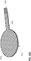
- FIGS. 15A/15B/15C/15D/15E illustrate an active element according to a third example embodiment of the present invention.
- the electric discharge between electrodes is further prevented by the inclusion of a second additional insulating layer 305.
- Figures 15A and 15B are top and bottom views of the active element, respectively.
- Figures 15C, 15D, and 15E are profile view sections of the active element across the axes AB, CD, and EF, respectively, as depicted in Figure 15B .
- Both types of active elements can be manufactured following existing industrial processes, like injection molding, roll to roll laminations, and cutting stages.
- active elements can be circular, hexagonal, squared, triangular, or can have any other shapes, like any complex polygonal shape. For the sake of clarity, only circular shapes appear in the examples presented.
- a third further example of said electrostatic actuator structure not being part of the present invention may comprise a 3D printed, or moulded, 3D grid made from proper polymers working as spring when compressed.
- magnets may be utilized so that for higher spring constant values, the repulsion of constrained magnets, placed facing each other with opposite polarity, could be employed as separation nodes.
Landscapes
- Engineering & Computer Science (AREA)
- General Engineering & Computer Science (AREA)
- Theoretical Computer Science (AREA)
- General Physics & Mathematics (AREA)
- Human Computer Interaction (AREA)
- Physics & Mathematics (AREA)
- Microelectronics & Electronic Packaging (AREA)
- Computer Hardware Design (AREA)
- Power Engineering (AREA)
- Analytical Chemistry (AREA)
- Chemical & Material Sciences (AREA)
- Micromachines (AREA)
- Thin Film Transistor (AREA)
Description
- The subject matter disclosed herein generally relates to an arrangement for facilitating a surface actuation mechanism in devices (e.g., systems or other apparatus) with a surface structure configured to facilitate electrically induced mechanical movement, including devices configured to provide, via electrically induced mechanical movement, various tactile effects such as tactile feedback. Specifically, the present disclosure addresses an active element structure for devices (e.g., systems or other apparatus) that have a surface structure configured to facilitate electrically induced mechanical movement.
- There are different techniques facilitating electrically induced mechanical movement in devices, such as e.g. consumer electronic devices. One common technique is the use of an Eccentric Rotating Mass (ERM) vibration motor. An ERM vibration motor moves small rotating mass that is off-center from the point of rotation. The rotation of the mass produces a centripetal force causing the entire motor to move and vibrate from side to side. Another common technique facilitating electrically induced mechanical movement is the use of a linear resonant actuator (LRA). A linear resonant actuator uses magnetic fields and electrical current to create a force to a coil, said coil driving a magnetic mass up and down against a spring. The movement of said magnetic mass moves the entire linear resonant actuator, thus producing electrically induced mechanical movement. Another common technique is the use of a piezoelectric actuator. A piezoelectric actuator produces a mechanical change in the piezoelectric material in response to an applied electric charge, said mechanical change producing electrically induced mechanical movement.
- In prior art, such electrically induced mechanical movement techniques have many disadvantages. These disadvantages include high power consumption, low durability, a shorter lifespan, complex design with external motors and/or masses as well as low scalability, and poor suitability to large area actuation.
- Previously some actuating solutions with elastic structures have been suggested.
- US Patent publication
US 8587541 B2 discloses one prior art solution for a method for actuating a tactile interface layer, wherein it has been suggested to use small hydraulic system to drive fluid in different reservoirs to generate deformations on a touch surface. The deformations that are to be generated by the hydraulic pumps could be readily observed with a finger touching the surface. - US Patent publication
US 9477076 B2 -
Japanese Patent application publication JP 2007-259663 A - Document
JPH08168099 A - Documents
JP5674222 B2 JPH06168099 A - Some embodiments are illustrated by way of example and not limitation in the figures of the accompanying drawings.
-
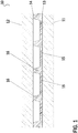
FIG. 1 is a conceptual diagram illustrating at least a portion of a single layer of the electrostatic actuator structure, according to one example embodiment of the present invention. -
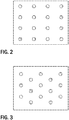
FIG. 2 illustrates a multitude of elastic support nodules according to one example embodiment of the present invention arranged in a spaced two-dimensional row/column grid array. -
FIG. 3 illustrates a multitude of elastic support nodules according to another example embodiment of the present invention arranged in a spaced triangular grid array. -
FIG. 4 is a conceptual diagram illustrating at least a portion of a single layer of the electrostatic actuator structure, according to another example embodiment of the present invention. -
FIG. 5 is a conceptual diagram illustrating at least a portion of an electrostatic actuator structure with four electrostatic actuation layers according to one example embodiment of the present invention. -
FIG. 6 is a conceptual diagram illustrating at least a portion of a single layer of the electrostatic actuator structure, according to a third example embodiment of the present invention. -
FIG. 7 is a conceptual diagram illustrating at least a portion of an electrostatic actuator structure with six electrostatic actuation layers according to another example embodiment of the present invention. -
FIG. 8 is a conceptual diagram illustrating at least a portion of an electrostatic actuator structure with six electrostatic actuation layers according to a third example embodiment of the present invention. -
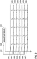
FIG. 9 is a conceptual diagram illustrating at least a portion of an electrostatic actuator structure with six electrostatic actuation layers according to a fourth example embodiment of the present invention. -
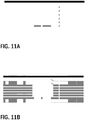
FIGS. 10A/10B illustrate at least two stacks of electrostatic actuation layers according to one example embodiment of the present invention. -
FIGS. 11A/11B illustrate at least two stacks of electrostatic actuation layers according to another example embodiment of the present invention with an additional firm structure. -
FIGS. 12A/12B/12C illustrate a conceptual diagram illustrating at least a portion of a single layer of the electrostatic actuator structure, according to a fifth example embodiment of the present invention. -
FIGS. 13A/13B/13C/13D illustrate an active element according to an example embodiment of the present invention. -
FIGS. 14A/14B/14C/14D /14E/14F illustrate an active element according to another example embodiment of the present invention. -
FIGS. 15A/15B/15C/15D/15E illustrate an active element according to a third example embodiment of the present invention. -
FIGS. 16A /16B /16C /16D illustrate an active element stack according to an example embodiment of the present invention. -
FIGS. 17A /17B /17C /17D/17E/17F illustrate a basic active element composing the active element stack according to another example embodiment of the present invention. -
FIGS. 18A /18B/18C illustrate a basic active element composing the active element stack according to a third example embodiment of the present invention. - The invention is defined by the appended claims.
- The presented new electrostatic actuator structure is a clear improvement over the prior art solutions. The new electrostatic actuator structure presents various innovative features, which make it suitable for actuating macroscopic structures, for example for tactile feedback applications. In particular, the actuation distances and amplitudes generated with the present invention are much greater and represent different scale levels when compared to the prior art solutions. The presented new electrostatic actuator structure is also suitable for new type of manufacturing methods such as injection molding.
- The modular nature of the presented new electrostatic actuator structure, with stacked identical module structures, allows the simple establishment of the final energy in the mechanical actuation (compression amplitude and force), by adding or removing active layers and adapting the power signal accordingly.
- The new electrostatic actuator structure described herein comprises a simple to manufacture insulator layer that has the suitable elastic structure incorporated in it and which can compress significantly within suitable voltage range. In our tests the overall area of the elastic nodules was optimally around 1% of the whole fluid space, this representing a substantive improvement when compared to the prior art solutions.
-
FIG. 1 is a conceptual diagram illustrating at least a portion of a single electrostatic actuation layer of the electrostatic actuator structure, according to one example embodiment of the present invention. The illustrated singleelectrostatic actuation layer 10 of the electrostatic actuator structure comprises afirst substrate film 11 and asecond substrate film 12. In the presented example embodiment ofFIG. 1 thefirst substrate film 11 and thesecond substrate film 12 have a thickness of 100 micrometers (100 µm). Thefirst substrate film 11 is normally of electrically insulating material but may also be intrinsically conductive or semi-conductive. In the presented example embodiment ofFIG. 1 thefirst substrate film 11 comprises a first conductive/semiconductive electrode layer 13 applied on top of thefirst substrate film 11, said first conductive/semiconductive electrode layer 13 being a part of a first electrode. Thesecond substrate film 12 is normally of electrically insulating material but may also be intrinsically conductive or semi-conductive. In the presented example embodiment ofFIG. 1 thesecond substrate film 12 comprises a second conductive/semiconductive electrode layer 14 applied on top of thesecond substrate film 12 said second conductive/semiconductive electrode layer 14 being a part of a second electrode. In the presented example embodiment ofFIG. 1 said first conductive/semiconductive electrode layer 13 is insulated. In an alternative embodiment of the present invention, said second conductive/semiconductive electrode layer 14 is insulated. Furthermore, in another alternative embodiment of the present invention said first conductive/semiconductive electrode layer 13 and said second conductive/semiconductive electrode layer 14 are both insulated. - An advantage of using semi-conductive material instead of fully conductive, i.e. having metallic conductivity, in said
first substrate film 11 and said secondfirst substrate film 12 and/or said first conductive/semiconductive electrode layer 13 and said second conductive/semiconductive electrode layer 14 may be that of the possibility to use more cost effective material especially in case if transparency is expected from the electrode, or if high flexibility and/or some elasticity is desired. The use of semi-conductive material also increases the safety of the device, preventing strong electric discharge in the case of accidental failure. - The
first substrate film 11 with said insulated first conductive/semiconductive electrode layer 13 has a layer of electrically insulatingelastic material 15, e.g. electrically insulatingelastomer coating 15 applied on top of said insulated first conductive/semiconductive electrode layer 13 of thefirst substrate film 11. Furthermore, there is a multitude ofelastic support nodules 16 arranged in a grid array and adhered on top, or forming part of the intrinsic structure of said layer of electrically insulatingelastic material 15 of said insulated first conductive/semiconductive electrode layer 13 of thefirst substrate film 11. - In examples not being part of the present invention, the
elastic base layer 15 may not be present, and only theelastic support nodules 16 will be present in the region between both conductive/semiconductive electrode layers, 13 and 14. - In the presented example embodiment of
FIG. 1 said layer of electrically insulatingelastic material 15 has a thickness of 20 micrometers (20 µm) and said multitude ofelastic support nodules 16 have a height of 60 micrometers (60 µm) and a diameter of 60 micrometers (60 µm). Said multitude ofelastic support nodules 16 may have a height to maximum width aspect ratio with a maximum value of two (2). The layer of electrically insulatingelastic material 15 and/or said multitude ofelastic support nodules 16 may be applied using a suitable deposition technique e.g. a thin film deposition technique. Said multitude ofelastic support nodules 16 may be made of silicon-based organic polymer, e.g. polydimethylsiloxane (PDMS). Said multitude ofelastic support nodules 16 may be arranged less than 10 mm distance apart from each other, preferably less than 2 mm distance apart from each other. Said multitude ofelastic support nodules 16 may have shape that is cone-like with thicker base than the tip. This form factor is especially suitable in injection molding to have smooth detachment of elastic layer from the mold. Said multitude ofelastic support nodules 16 may e.g. be arranged in a grid array of a spaced two-dimensional row/column grid array as illustrated inFIG. 2 . Alternatively, said multitude ofelastic support nodules 16 may be arranged in a grid array of a spaced triangular grid array as illustrated inFIG. 3 . - After said multitude of
elastic support nodules 16 have been applied on thefirst substrate film 11 thesecond substrate film 12 with said second conductive/semiconductive electrode layer 14 is turned upside down and placed on top of the multitude ofelastic support nodules 16 to form an electrostatic actuation layer. Before placing saidsecond substrate film 12 on top of thefirst substrate film 11 and the multitude ofelastic support nodules 16 there may be adhesive applied to saidsecond substrate film 12 and/or to said multitude ofelastic support nodules 16. As saidfirst substrate film 11 and saidsecond substrate film 12 have been stacked one above the other as an electrostatic actuation layer, the distance between said first conductive/semiconductive electrode layer 13 and said second conductive/semiconductive electrode layer 14, i.e. the distance between electrodes, in said electrostatic actuation layer may be less than 1000 micrometers (1000 µm) and preferably less than 200 micrometers (200 µm). In said electrostatic actuation layer the presented example embodiment ofFIG. 1 said distance between said first and second conductive/semiconductive electrode layers 13, 14 is 80 micrometers (80 µm). - In said electrostatic actuation layer, said multitude of
elastic support nodules 16 provide a compression space between said first and second conductive/semiconductive electrode layers 13, 14, said compression space not entirely filled with solid material. In the presented example embodiment ofFIG. 1 said compression space is 80 micrometers (80 µm) thick and has a 20 micrometers (20 µm) thick electrically insulatingelastic material layer 15 thus leaving a space gap of 60 micrometers (60 µm), which space gap of said compression space may be filled with fluid, e.g. air, nitrogen or a dielectric liquid for example dielectric hydraulic fluid. In the presented example embodiment at least one of said electrostatic actuation layers may also comprise a grid array comprising a multitude of limiting nodules, said multitude of limiting nodules arranged between elastic support nodules and between said first substrate film and said second substrate film, for limiting the compression of said electrostatic actuator structure. In the presented example embodiment the surfaces of said first and second conductive/semiconductive electrode layers 13, 14 on both sides of said space gap and theelastic support nodules 16 may be inherently hydrophobic or hydrophobically or superhydrophobically coated or hydrophobically or superhydrophobically treated. - The electrostatic actuator structure according to the present invention is arranged to compress when sufficient voltage difference is applied between said at least a first electrode and a second electrode. Said electrostatic actuator structure may be embedded as part of a flexible substrate. Said electrostatic actuator structure is not necessarily flat, and can be flexible, and may be embedded as part of a rigid, not necessarily flat, or flexible substrate. The illustrated single
electrostatic actuation layer 10 of the electrostatic actuator structure has an overall thickness of 280 micrometers (280 µm) added with the thickness of said first and second conductive/semiconductive electrode layers 13, 14 and the thickness of said adhesive 107 this giving an overall thickness of approximately 290 micrometers (290 µm). - The inventors have observed that the system is very specific for the nodule spacing and dimensions. For the macroscopic actuation applications, which the system has been designed for, for example, dimensions of 100-micrometer tall nodules with 100-micrometer diameter and 1 millimeter spacing, work well with typical silicone rubber hardness. Such nodules may for example compress 10 to 30 micrometers when potential difference of around 1 KV voltage is applied. The amplitude and strength of the actuation can be increased by stacking several layers on top of one another.
-
FIG. 4 is a conceptual diagram illustrating at least a portion of a single electrostatic actuation layer of the electrostatic actuator structure, according to another example embodiment of the present invention. The illustrated singleelectrostatic actuation layer 20 of the electrostatic actuator structure comprises afirst substrate film 21 and asecond substrate film 22. In the presented example embodiment ofFIG. 4 thefirst substrate film 21 has a thickness of 100 micrometers (100 µm) and thesecond substrate film 22 has a thickness of 175 micrometers (175 µm). Thefirst substrate film 21 is normally of electrically insulating material but may also be intrinsically conductive or semi-conductive. In the presented example embodiment ofFIG. 4 thefirst substrate film 21 comprises a first conductive/semiconductive electrode layer 23 applied on top of thefirst substrate film 21, said first conductive/semiconductive electrode layer 23 being a part of a first electrode. Thesecond substrate film 22 is normally of electrically insulating material but may also be intrinsically conductive or semi-conductive. In the presented example embodiment ofFIG. 4 thesecond substrate film 22 comprises a second conductive/semiconductive electrode layer 24 applied on top of thesecond substrate film 22 said second conductive/semiconductive electrode layer 24 being a part of a second electrode. In the presented example embodiment ofFIG. 4 said first conductive/semiconductive electrode layer 23 is insulated. In an alternative embodiment of the present invention, said second conductive/semiconductive electrode layer 24 is insulated. Furthermore, in another alternative embodiment of the present invention said first conductive/semiconductive electrode layer 23 and said second conductive/semiconductive electrode layer 24 are both insulated. - An advantage of using semi-conductive material instead of fully conductive, i.e. having metallic conductivity, in said
first substrate film 21 and said secondfirst substrate film 22 and/or said first conductive/semiconductive electrode layer 23 and said second conductive/semiconductive electrode layer 24 may be that of the possibility to use more cost effective material especially in case if transparency is expected from the electrode, or if high flexibility and/or some elasticity is desired. The use of semi-conductive material also increases the safety of the device, preventing strong electric discharge in the case of accidental failure. - The
first substrate film 21 with said insulated first conductive/semiconductive electrode layer 23 has a layer of electrically insulatingelastic material 25, e.g. electrically insulatingelastomer coating 25 applied on top of said insulated first conductive/semiconductive electrode layer 23 of thefirst substrate film 21. Furthermore, there is a multitude ofelastic support nodules 26 arranged in a grid array and adhered on top, or forming part of the intrinsic structure of said layer of electrically insulatingelastic material 25 of said insulated first conductive/semiconductive electrode layer 23 of thefirst substrate film 21. - In examples not being part of the present invention, the
elastic base layer 25 may not be present, and only theelastic support nodules 26 will be present in the region between both conductive/semiconductive electrode layers, 23 and 24. - In the presented example embodiment of
FIG. 4 said layer of electrically insulatingelastic material 25 has a thickness of 20 micrometers (20 µm) and said multitude ofelastic support nodules 26 have a height of 150 micrometers (150 µm). Said multitude ofelastic support nodules 26 may have a height to maximum width aspect ratio with a maximum value of two (2). The layer of electrically insulatingelastic material 25 and/or said multitude ofelastic support nodules 26 may be applied using a suitable microfabrication technique e.g. a thin film deposition technique. Said multitude ofelastic support nodules 26 may be made of silicon-based organic polymer, e.g. polydimethylsiloxane (PDMS). Said multitude ofelastic support nodules 26 may be arranged less than 10 mm distance apart from each other, preferably less than 2 mm distance apart from each other. Said multitude ofelastic support nodules 26 may have shape that is cone-like with thicker base than the tip. This form factor is especially suitable in injection molding to have smooth detachment of elastic layer from the mold. Said multitude ofelastic support nodules 26 may e.g. be arranged in a grid array of a spaced two-dimensional row/column grid array as illustrated inFIG. 2 . Alternatively, said multitude ofelastic support nodules 26 may be arranged in a grid array of a spaced triangular grid array as illustrated inFIG. 3 . - The
second substrate film 22 is microfabricated e.g. etched in order to providewells 28 to saidsecond substrate film 22, saidwells 28 arranged to match the multitude ofelastic support nodules 26 of thefirst substrate film 21. Thewells 28 may be microfabricated using a suitable microfabrication technique e.g. an anisotropic wet etching technique. The microfabricatedsecond substrate film 22 with said second conductive/semiconductive electrode layer 24 is turned upside down and placed on top of the multitude ofelastic support nodules 26 of thefirst substrate film 21 so that thewells 28 coincide with the multitude ofelastic support nodules 26 to form an electrostatic actuation layer. In said electrostatic actuation layer, theelastic support nodules 26 reside in saidwells 28. Before placing saidsecond substrate film 22 on top of the multitude ofelastic support nodules 26 there may be adhesive 27 applied to saidwells 28 and/or to said multitude ofelastic support nodules 26. In the presented example embodiment ofFIG. 4 said depth of saidwells 28 is 90 micrometers (90 µm). Other suitable depths may be used also depending on the thickness of thesecond substrate film 22 to be microfabricated. - As said
first substrate film 21 and saidsecond substrate film 22 have been stacked one above the other as an electrostatic actuation layer, the distance between said first conductive/semiconductive electrode layer 23 and said second conductive/semiconductive electrode layer 24, i.e. the distance between electrodes, in said electrostatic actuation layer may be less than 1000 micrometers (1000 µm) and preferably less than 200 micrometers (200 µm). In said electrostatic actuation layer the presented example embodiment ofFIG. 4 said distance between said first and second conductive/semiconductive electrode layers 23, 24 is 80 micrometers (80 µm). Due to thewells 28 of saidsecond substrate film 22 matching the multitude ofelastic support nodules 26 of saidfirst substrate film 21 said distance between said first and second conductive/semiconductive electrode layers 23, 24 is considerably less than the height of the multitude ofelastic support nodules 26. This is the main advantage of this type of configuration, since the shorter distance between electrodes allows stronger electrostatic compression forces for a same nodule height. Eventually, this leads to higher compressing ratios for similar actuation forces. - In said electrostatic actuation layer, said multitude of
elastic support nodules 26 provide a compression space between said first and second conductive/semiconductive electrode layers 23, 24, said compression space not entirely filled with solid material. In the presented example embodiment ofFIG. 4 said compression space is 80 micrometers (80 µm) thick and has a 20 micrometers (20 µm) thick electrically insulatingelastic material layer 25 thus leaving a space gap of 60 micrometers (60 µm), which space gap of said compression space may be filled with fluid, e.g. air, nitrogen or a dielectric liquid for example dielectric hydraulic fluid. In the presented example embodiment at least one of said electrostatic actuation layers may also comprise a grid array comprising a multitude of limiting nodules, said multitude of limiting nodules arranged between elastic support nodules and between said first substrate film and said second substrate film, for limiting the compression of said electrostatic actuator structure. In the presented example embodiment the surfaces of said first and second conductive/semiconductive electrode layers 23, 24 on both sides of said space gap of said compression space and theelastic support nodules 26 may be inherently hydrophobic or hydrophobically or superhydrophobically coated or hydrophobically or superhydrophobically treated. - The electrostatic actuator structure according to the present invention is arranged to compress when sufficient voltage difference is applied between said at least a first electrode and a second electrode. Said electrostatic actuator structure may be embedded as part of a flexible substrate. Said electrostatic actuator structure is not necessarily flat, can be flexible, and may be embedded as part of a rigid, not necessarily flat, or flexible substrate. The illustrated single
electrostatic actuation layer 20 of the electrostatic actuator structure has an overall thickness of 355 micrometers (355 µm) added with the thickness of said first and second conductive/semiconductive electrode layers 23, 24 and the thickness of said adhesive 27 this giving an overall thickness of approximately 365 micrometers (365 µm). -
FIG. 5 is a conceptual diagram illustrating at least a portion of an electrostatic actuator structure with four electrostatic actuation layers according to one example embodiment of the present invention. The illustrated electrostatic actuator structure comprises four electrostatic actuation layers 211 - 214. In the presented example embodiment ofFIG. 5 each of the electrostatic actuation layers 211-214 comprise a first substrate film with a first conductive/semiconductive electrode layer said first conductive/semiconductive electrode layer being a part of afirst electrode 230, and a second substrate film with a second conductive/semiconductive electrode layer said second conductive/semiconductive electrode layer being a part of asecond electrode 240, at least one of said first and second conductive/semiconductive electrode layers being insulated from the other conductive/semiconductive electrode layers, and a grid array comprising a multitude of elastic support nodules, said multitude of elastic support nodules arranged between said first substrate film and said second substrate film, so that there is arranged a compression space between said first and second conductive/semiconductive electrode layers, said compression space not entirely filled with solid material. The electrostatic actuator structure according to the present invention may also comprise aHigh Voltage Driver 250, e.g. a High Voltage Driver with a Flyback-mode boost converter. - In the presented example embodiment of
FIG. 5 each of the electrostatic actuation layers 211-214 are stacked one above the other so that similar structural elements of said electrostatic actuation layers 211-214 coincide at least partially, preferably coincide fully. The electrostatic actuator structure according to the present invention is arranged to compress when sufficient voltage difference is applied between saidfirst electrode 230 and saidsecond electrode 240. Due to the coinciding, adhered and joint structure of the said electrostatic actuation layers 211-214 the compression effect of said electrostatic actuator structure is increased substantially as function of the number of coinciding layers. With the help of the adhered and joint structure of the said electrostatic actuation layers 211-214 the hole above is avoided and the potential reduction of the effect due to the potential inter-pillar swallowing for air compression is covered. Furthermore, potential inter layer bouncing or nonuniform separation is also avoided. - As each of the electrostatic actuation layers 211-214 have an overall thickness of approximately 365 micrometers (365 µm) the thickness for the electrostatic actuator structure with four electrostatic actuation layers according to presented example embodiment is approximately four times 365 micrometers (4 x 365 µm) this giving for the electrostatic actuator structure a total thickness of approximately 1.46 millimeters (1.46 mm). The electrostatic actuator structure according to the present invention may be hermetically sealed.
- The described compressing nodule structure together with the hermetic sealing, allows using the compression of the layers as pneumatic pump structure. The gas or liquid material can be used to actuate various elastic structures that are affected by the pressure, creating a textured surface or actuating some part of system via pneumatic or hydraulic means.
-
FIG. 6 is a conceptual diagram illustrating at least a portion of a single electrostatic actuation layer of the electrostatic actuator structure, according to a third example embodiment of the present invention. The illustrated singleelectrostatic actuation layer 30 of the electrostatic actuator structure comprises afirst substrate film 31 and asecond substrate film 32. In the presented example embodiment ofFIG. 6 thefirst substrate film 31 has a thickness of 100 micrometers (100 µm) and thesecond substrate film 32 has a thickness of 175 micrometers (175 µm). Thefirst substrate film 31 is normally of electrically insulating material but may also be intrinsically conductive or semi-conductive. In the presented example embodiment ofFIG. 6 thefirst substrate film 31 comprises a first conductive/semiconductive electrode layer 33 applied on top of thefirst substrate film 31, said first conductive/semiconductive electrode layer 33 being a part of a first electrode. Thesecond substrate film 32 is normally of electrically insulating material but may also be intrinsically conductive or semi-conductive. In the presented example embodiment ofFIG. 6 thesecond substrate film 32 comprises a second conductive/semiconductive electrode layer 34 applied on top of thesecond substrate film 32 said second conductive/semiconductive electrode layer 34 being a part of a second electrode. One or both of the said first conductive/semiconductive electrode layer 33 and said second conductive/semiconductive electrode layer 34 are insulated. - An advantage of using semi-conductive material instead of fully conductive, i.e. having metallic conductivity, in said
first substrate film 31 and said secondfirst substrate film 32 and/or said first conductive/semiconductive electrode layer 33 and said second conductive/semiconductive electrode layer 34 may be that of the possibility to use more cost effective material especially in case if transparency is expected from the electrode, or if high flexibility and/or some elasticity is desired. - The
first substrate film 31 with said insulated first conductive/semiconductive electrode layer 33 has a layer of electrically insulatingelastic material 35, e.g. electrically insulatingelastomer coating 35 applied on top of said insulated first conductive/semiconductive electrode layer 33 of thefirst substrate film 31. Furthermore, there is a multitude ofelastic support nodules 36 arranged in a grid array and adhered on top, or forming part of the intrinsic structure of said layer of electrically insulatingelastic material 35 of said insulated first conductive/semiconductive electrode layer 33 of thefirst substrate film 31. In the presented example embodiment ofFIG. 6 said layer of electrically insulatingelastic material 35 has a thickness of 20 micrometers (20 µm) and said multitude ofelastic support nodules 36 have a height of 80 micrometers (80 µm). Said multitude ofelastic support nodules 36 may have a height to maximum width aspect ratio with a maximum value of two (2). The layer of electrically insulatingelastic material 35 and/or said multitude ofelastic support nodules 36 may be applied using a suitable microfabrication technique e.g. a thin film deposition technique. Said multitude ofelastic support nodules 36 may be made of silicon-based organic polymer, e.g. polydimethylsiloxane (PDMS). Said multitude ofelastic support nodules 36 may be arranged less than 10 mm distance apart from each other, preferably less than 2 mm distance apart from each other. Said multitude ofelastic support nodules 16 may have shape that is cone-like with thicker base than the tip. This form factor is especially suitable in injection molding to have smooth detachment of elastic layer from the mold. Said multitude ofelastic support nodules 36 may e.g. be arranged in a grid array of a spaced two-dimensional row/column grid array as illustrated inFIG. 2 . Alternatively, said multitude ofelastic support nodules 36 may be arranged in a grid array of a spaced triangular grid array as illustrated inFIG. 3 . - Furthermore, the electrostatic actuator structure according to the present example embodiment comprises
gas reservoirs 37, e.g. air reservoirs allowing decreased overall air compression when the air compresses or moves from a compressing layer. Thesecond substrate film 32 is microfabricated e.g. etched in order to providegas reservoirs 37,e.g. air reservoirs 37, to saidsecond substrate film 32, saidgas reservoirs 37 arranged to reduce the compression ratio of air volume. Thegas reservoirs 37 may be microfabricated using a suitable microfabrication technique e.g. an anisotropic wet etching technique. The microfabricatedsecond substrate film 32 with said second conductive/semiconductive electrode layer 34 is turned upside down and placed on top of the multitude ofelastic support nodules 36 to form an electrostatic actuation layer. In the presented example embodiment ofFIG. 6 said depth of saidgas reservoirs 37 is 90 micrometers (90 µm). Other suitable depths may be used also depending on the thickness of thesecond substrate film 32 to be microfabricated. Furthermore, the depth of saidgas reservoirs 37 can be the same as the thickness of thesecond substrate film 32, so that they form holes through it. - The inventors have observed that the system is very specific for the nodule spacing and dimensions. For the macroscopic actuation applications, which the system has been designed for, for example, dimensions of 100-micrometer tall nodules with 100-micrometer diameter and 1 millimeter spacing, work well with typical silicone rubber hardness. Such nodules may for example compress 10 to 30 micrometers when potential difference of around 1 KV voltage is applied. The amplitude and strength of the actuation can be increased by stacking several layers on top of one another.
- In addition, the resistance of the semi conductive layer may be selected so that the said actuator structure can be positioned on top of capacitive touch sensor or capacitive touch panel and allow the touch sensor sense through the layer. This is possible because the capacitive touch sensors or capacitive touch panel typically uses over 100 kHz signals for sensing purposes, whereas the present actuator is typically driven with signals below 500 Hz. Therefore it is possible to make the actuator electrodes of material that is semi conductive for example between 100kOhm/square to 100MOhm/square of surface resistance, wherein they can be charged sufficiently fast for the actuator to actuate, but they will appear as insulating layer to touch panels much higher frequency sensing signal. The semi-conductiveness of a first substrate film and a second substrate film may be selected so that said first substrate film and said second substrate film appear as insulating layer to a higher frequency sensing signal.
- The use of semi conductive material may have yet another benefit, in case the said actuator is exposed to for example a puncture risk by conductive object, the semi conductive material works as natural current limiting method providing additional safety benefit.
-
FIG. 7 is a conceptual diagram illustrating at least a portion of an electrostatic actuator structure with six electrostatic actuation layers according to another example embodiment of the present invention. The illustrated electrostatic actuator structure comprises six electrostatic actuation layers 111-116. In the presented example embodiment ofFIG. 7 each of the electrostatic actuation layers 111-116 comprise a first substrate film with a first conductive/semiconductive electrode layer said first conductive/semiconductive electrode layer being a part of afirst electrode 130, and a second substrate film with a second conductive/semiconductive electrode layer said second conductive/semiconductive electrode layer being a part of asecond electrode 140, at least one of said first and second conductive/semiconductive electrode layers being insulated from the other conductive/semiconductive electrode layers, said electrostatic actuation layers 111-116 being stacked one above another as a stack of electrostatic actuation layers so that in the middle of said stack a bifunctional substrate film forms a first substrate film or a second substrate film for two of said electrostatic actuation layers 111-116, one below said bifunctional substrate film and another above said bifunctional substrate film. The electrostatic actuator structure according to the present invention may also comprise aHigh Voltage Driver 150, e.g. a High Voltage Driver with a Flyback-mode boost converter. Furthermore, each of the substrate films in said stack of electrostatic actuation layers may comprise an embedded connection element 121-127, e.g. an embedded metal wire 121-127, said embedded connection element 121-127 connecting the conductive/semiconductive electrode layer/layers to saidHigh Voltage Driver 150. In the middle of said stack of electrostatic actuation layers, the embedded connection elements 122-126 connect the conductive/semiconductive electrode layers of said bifunctional substrate film together and to saidHigh Voltage Driver 150. - Each of the electrostatic actuation layers 111-116 also comprise a grid array comprising a multitude of elastic support nodules, said multitude of elastic support nodules arranged between said first substrate film and said second substrate film, so that there is arranged a compression space between said first and second conductive/semiconductive electrode layers, said compression space not entirely filled with solid material.
-
FIG. 8 is a conceptual diagram illustrating at least a portion of an electrostatic actuator structure with six electrostatic actuation layers according to a third example embodiment of the present invention. The illustrated electrostatic actuator structure comprises six electrostatic actuation layers 131-136. In the presented example embodiment ofFIG. 8 each of the electrostatic actuation layers 131-136 comprise a first substrate film with a first conductive/semiconductive electrode layer said first conductive/semiconductive electrode layer being a part of afirst electrode 130, and a second substrate film with a second conductive/semiconductive electrode layer said second conductive/semiconductive electrode layer being a part of asecond electrode 140, at least one of said first and second conductive/semiconductive electrode layers being insulated from the other conductive/semiconductive electrode layers, said electrostatic actuation layers 131-136 being stacked one above another as a stack of electrostatic actuation layers so that in the middle of said stack a bifunctional substrate film forms a first substrate film or a second substrate film for two of said electrostatic actuation layers 131-136, one below said bifunctional substrate film and another above said bifunctional substrate film. Furthermore, in the middle of said stack of electrostatic actuation layers a bifunctional conductive/semiconductive electrode layer of said bifunctional substrate film is arranged to act as a conductive/semiconductive electrode layer for a two of said electrostatic actuation layers 131-136, one below said bifunctional conductive/semiconductive electrode layer and another above said bifunctional conductive/semiconductive electrode layer. - The electrostatic actuator structure according to the present invention may also comprise a
High Voltage Driver 150, e.g. a High Voltage Driver with a Flyback-mode boost converter. Furthermore, each of the substrate films in said stack of electrostatic actuation layers may comprise an embedded connection element 141-147, said embedded connection element 141-147 connecting the conductive/semiconductive electrode layer/coatings to saidHigh Voltage Driver 150. - Each of the electrostatic actuation layers 131-136 also comprise a grid array comprising a multitude of elastic support nodules, said multitude of elastic support nodules arranged between said first substrate film and said second substrate film, so that there is arranged a compression space between said first and second conductive/semiconductive electrode layers, said compression space not entirely filled with solid material.
-
FIG. 9 is a conceptual diagram illustrating at least a portion of an electrostatic actuator structure with six electrostatic actuation layers according to a fourth example embodiment of the present invention. The illustrated electrostatic actuator structure comprises six electrostatic actuation layers 151-156. In the presented example embodiment ofFIG. 9 each of the electrostatic actuation layers 151-156 comprise a first substrate film with a first conductive/semiconductive electrode layer said first conductive/semiconductive electrode layer being a part of afirst electrode 130, and a second substrate film with a second conductive/semiconductive electrode layer said second conductive/semiconductive electrode layer being a part of asecond electrode 140, at least one of said first and second conductive/semiconductive electrode layers being insulated from the other conductive/semiconductive electrode layers, said electrostatic actuation layers 151-156 being stacked one above another as a stack of electrostatic actuation layers so that in the middle of said stack a bifunctional electrically insulating elastic material layer forms a first substrate film or a second substrate film for two of said electrostatic actuation layers 151-156, one below said bifunctional electrically insulating elastic material layer and another above said bifunctional electrically insulating elastic material layer. Furthermore, in the middle of said stack of electrostatic actuation layers a bifunctional conductive/semiconductive electrode layer of said bifunctional electrically insulating elastic material layer is arranged to act as a conductive/semiconductive electrode layer for a two of said electrostatic actuation layers 151-156, one below said bifunctional conductive/semiconductive electrode layer and another above said bifunctional conductive/semiconductive electrode layer. - The electrostatic actuator structure according to the present invention may also comprise a
High Voltage Driver 150, e.g. a High Voltage Driver with a Flyback-mode boost converter. Furthermore, each on the substrate films in said stack of electrostatic actuation layers may comprise an embedded connection element 161-167, said embedded connection element 161-167 connecting the conductive/semiconductive electrode layer/coatings to saidHigh Voltage Driver 150. - Each of the electrostatic actuation layers 151-156 also comprise a grid array comprising a multitude of elastic support nodules, said multitude of elastic support nodules arranged between said first substrate film and said second substrate film, so that there is arranged a compression space between said first and second conductive/semiconductive electrode layers, said compression space not entirely filled with solid material.
- Said two or more electrostatic actuation layers of said electrostatic actuator structure may comprise several electrostatic actuation layers stacked one above the other to form at least two stacks of electrostatic actuation layers as illustrated in
FIG. 10A, FIG. 10B ,FIG. 11A and FIG. 11B . In the presented example embodiments the surfaces of said first and second conductive/semiconductive electrode layers on both sides of said space gap and the elastic support nodules may be inherently hydrophobic or hydrophobically or superhydrophobically coated or hydrophobically or superhydrophobically treated. -
FIGS. 10A/10B andFIGS. 11A/11B present an electrostatic actuator structure with at least two stacks of electrostatic actuation layers with at least one gas reservoir, e.g. air reservoir, arranged between said at least two stacks of electrostatic actuation layers and an elastic surface layer arranged on top of said at least two stacks of electrostatic actuation layers and on top of said at least one gas reservoir. InFIGS. 11A/11B , said electrostatic actuator structure also has an additional firm structure on top of said elastic surface layer.FIGS. 10A /11A present said electrostatic actuator structure when being in a state of rest.FIGS. 10B /11B present said electrostatic actuator structure when being compressed so that said elastic surface layer on top of said at least one gas reservoir bulges accordingly. -
FIGS. 12A/12B/12C illustrate a conceptual diagram illustrating at least a portion of a single layer of the electrostatic actuator structure, according to a fifth example embodiment of the present invention. InFIGS. 12A/12B/12C , said electrostatic actuator structure has a flexible upper substrate. -
FIG. 12A presents said electrostatic actuator structure when being in a state of rest.FIG. 12B presents said electrostatic actuator structure when being partially compressed.FIG. 12C presents said electrostatic actuator structure when being fully compressed. InFIGS. 12B/12C , as the flexible upper substrate of said electrostatic actuator structure is being compressed the excess gas bulges in the positions of support nodules. -
FIGS. 13A/13B/13C/13D illustrate an active element according to an example embodiment of the present invention.Figures 13A and 13B are top and bottom views of an active element, respectively.Figures 13C and 13D are profile view sections of the active element across the axes AB and CD, respectively, as depicted inFigure 13B . - In
FIGS. 13A/13B/13C/13D , the electrode layer is depicted asreference 101.Nodules 103, orpillars 103, which are all connected by base layer of the same material, with which base layer of the same material they form a single unit that represents anelastic layer 102. Nevertheless, this is only one example, and in other implementations not being part of the present invention the nodules, or the pillars, may be individually distributed forming the compressive layer without connection between them, or may be connected by a grid structure of the same or a different material. The presented active elements are intended for stacking and driving a charge between adjacent ones in order to generate attraction between them. A critical problem in electrostatic systems, like the ones in present invention, is that, when they are subjected to a relatively high potential difference, electric discharge may occur between the electrode layers. To address this problem, each one of the configurations presented on the different example embodiments must be specifically adapted, when the applied voltage difference is sufficiently high, to prevent the dielectric breakdown of the fluid between the electrodes, as described above. In the current example embodiment, the non-conductiveelastic layer 102 has a larger surface area than theelectrode layer 101, and this area difference is sufficient to prevent the electric discharge between electrodes if the applied potential difference is low enough. The electrodes may be insulated, in this way, using the same material that forms the elastic nodules and may form part of the same layer, but electrical insulation can also be achieved or improved by covering completely the exposed electrode areas, in contact with the fluid between the electrodes, with the an additional insulating layer made of a highly electrically-insulating material, such as polymer or polyimide, e.g. Kapton, thus forming layers to prevent electrical discharges between two or more electrodes of the active elements. This later configuration is illustrated in the following example embodiment ofFIGS. 14A/14B/14C/14D /14E/14F . -
FIGS. 14A/14B/14C/14D /14E/14F illustrate an active element according to the present invention. According to the present invention, the electric discharge between electrodes is further prevented by the inclusion of an additional insulating layer.Figures 14A and 14B are top and bottom views of the active element, respectively.Figures 14C and 14D /14E/14F are profile view sections of the active element across the axes AB and CD,FIGS. 14D /14E/14F presenting different alternative configurations, respectively, as depicted inFigure 14B . - In
FIGS. 14A/14B/14C/14D /14E/14F , an electrode layer is depicted asreference 201.Nodules 203, orpillars 203, which, together with a base layer of the same material, form an integral part of anelastic layer 202. An insulating layer is illustrated asreference 204, and the surface of said insulatinglayer 204 extends beyond the edge of the area of theelectrode 201, making direct contact with the non-conductiveelastic layer 202 in this region for electrical insulation. The position of theelectrode 201, between the elastic 202 and insulating 204 layers, is indicated as a thin dotted line inFigures 14A and 14B . - The different alternative configurations of
FIGS. 14D /14E/14F represent examples of different alternatives for the structure of the exposed region of theelectrode layer 201, which is necessary for electric connection. They all target at allowing the electrical contact from both sides of the active element, which is very useful in some basic stack configurations, as the one illustrated inFIGS. 16A /16B /16C /16D described below. - In
Figure 14D , theelectrode layer 201, at the electric-contact region, bends after the edge of the insulatinglayer 204, and extends over its upper side, keeping direct contact with its upper surface. The configuration illustrated in this figure is only possible if the conductivity of the electrode layer is not compromised by its high bending at the edge. For example, a solid metallic layer, like copper foil, is a suitable material for some embodiments. - In
Figure 14E , theelectrode layer 201 is constantly in contact with the bottom side of the insulatinglayer 204, and it bends together with it, at the contact region, exposing the electrode from both sides of the active element. Depending on the maximum curvature at the bending edge of these layers, this configuration will allow the use of much thinner electrode layers, like e.g. thin-film coating. - In
Figure 14F , an extremely thin electrode layer (not visible in the figure) is constantly in contact with the bottom side of the insulatinglayer 204. A thickerconductive layer 205 is placed at the contact region, in direct electric contact with the electrode layer at the bottom of the insulatinglayer 204, and bending after the edge, thus facilitating electric contact from both sides of the active element in this region. -
FIGS. 15A/15B/15C/15D/15E illustrate an active element according to a third example embodiment of the present invention. In presented another example embodiment ofFIGS. 15A/15B/15C/15D/15E , the electric discharge between electrodes is further prevented by the inclusion of a second additional insulatinglayer 305.Figures 15A and 15B are top and bottom views of the active element, respectively.Figures 15C, 15D, and 15E are profile view sections of the active element across the axes AB, CD, and EF, respectively, as depicted inFigure 15B . - In
FIGS. 15A/15B/15C/15D/15E , an electrode layer is depicted asreference 301.Nodules 303, orpillars 303, which, together with a base layer of the same material, form an integral part of anelastic layer 302. A first insulatinglayer 304, and its surface extends beyond the edge of the area of theelectrode 301, making direct contact with the non-conductiveelastic layer 302, or with an additional insulatinglayer 305 in the extended contact region, for electrical insulation. The position of theelectrode 301, between the elastic layer 302 (or insulating layer 305) and insulating 304 layers, is indicated as a thin dotted line inFigures 15A and 15B . - The main difference between the examples in
FIGS. 14A/14B/14C/14D /14E/14F andFIGS. 15A/15B/15C/15D/15E is that the part of the non-conductiveelastic layer 202 that extended along the narrow straight area towards the contact region inFIGS. 14A/14B/14C/14D /14E/14F has been replaced by a second insulatinglayer 305 inFIGS. 15A/15B/15C/15D/15E . This can be beneficial for simpler, or more economical, manufacturing, or for a more robust final product. It can also help to restrict the moving or bending of the electrode layer in this connecting region. -
FIGS. 16A /16B /16C /16D illustrate an active element stack according to an example embodiment of the present invention.Figures 16A and16B are perspective views of a basic active element composing the active element stack, and of one possible configuration of the final active element stack, respectively.Figures 16C and16D are profile view sections of the active element stack across the axes AB and CD, respectively, as depicted inFigure 16B . InFIGS. 16A /16B /16C /16D , the electrode layers are presented aselements 401, the elastic layers are presented aselements 402, including theircorresponding pillars 403, and the insulating layers are presented aselements 404. - In
FIGS. 16A /16B /16C /16D , the contact points for electrical connection are positioned in a 180 deg configuration (following a straight line), but, depending of the final arrangement of the sensor or of the actuator (sensors/actuators), they can be placed forming any other angle, as soon as they do not overlap between them. - The electric contact between the
electrodes 401 at each side of the active element stack can be made by soldering them together, or by using some mechanical clamping, like e.g. an alligator clip, or by clamping them between small permanent magnets. The robustness and safety of the electric connection can be increased by sealing it with solid material (like e.g. the one in the elastic layer). -
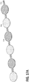
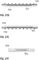
FIGS. 17A /17B /17C /17D/17E/17F illustrate a basic active element composing the active element stack according to another example embodiment of the present invention.Figures 17A and17B are perspective and top views of this new active element, respectively.Figures 17C ,17D, 17E and 17F are profile view sections of the active element across the axes AB, CD, EF, and GH, respectively, as depicted inFigure 17B . InFIGS. 17A /17B /17C /17D/17E/17F , the electrode layer is depicted asreference 501, the elastic layers (including the pillars) asreferences 502, and the insulating layers asreferences 504. The position of theelectrode layer 501, between theelastic layer 502 and insulating 504 layers (or between insulatinglayers 504 ofFigure 17F ), is indicated as a thin dotted line inFigure 17B . -
FIGS. 18A /18B/18C illustrate a possible staking configuration for the active elements described in the former example embodiment of the present invention. In these figures, the basic active elements described inFIGS. 17A /17B /17C /17D/17E/17F are stacked in a configuration, where only two basic active elements are overlapped in an interlaced configuration.Figure 18A represent a perspective view of a possible stacking configuration of the basic active elements described inFIGS. 17A /17B /17C /17D/17E/17F , andFigures 18B and 18C are profile view sections of the stack across the axes AB and CD, respectively, as depicted inFigure 18A . InFIGS. 18A /18B/18C , the electrode layers are presented asreferences 601, the elastic layers are presented as references 602 (including their corresponding pillars), and the insulating layers are presented asreferences 604. - As commented above, the number of basic active elements (like the ones in
FIGS. 17A /17B /17C /17D/17E/17F ) per stack, in this example embodiment of the present invention, is two. However, as can be seen inFIGS. 18A /18B/18C , the number of active layers, which is equivalent to the number of elastic layers (502 or 602), is determined by the length of the basic active element, i.e. by the number of elastic layers that it incorporates. - The main advantages of the stack of active elements described in
FIGS. 18A /18B/18C , with respect to the one described inFIGS. 16B /16C /16D , are the presence of a single contact point for electrical connection, per electrode layer, and a higher stack robustness. In addition, the length of the active element described inFIGS. 17A /17B /17C /17D/17E/17F can be adjusted by simply cutting a longer stripe roll at a specific length. However, this option requires that a new contact point for electrical connection will be available after cutting, which e.g. can be achieved by letting exposed part of theelectrode layer 501 in the areas between the elastic layers 502. - Both types of active elements, the ones in
Figures 13A to 16D , or the ones inFigures 17A to 18C , can be manufactured following existing industrial processes, like injection molding, roll to roll laminations, and cutting stages. - A stack of active elements can work as a single actuation element, or several stacks (from each configuration -
FIGS. 16A /16B /16C /16D and18A /18B/18C - or incorporating a mixture of both) can be connected in parallel to a same electric signal source. The horizontal distribution of multiple stacks, as described above, may facilitate the production of different actuation in different localized areas. - The source can provide the signal to each stack by e.g. connecting them to a conductive mesh, or grid, of cables or laminated conductors, or to a printed circuit board, or to any other configuration.
- For all the layers that appear in direct contact with each other in all the figures, it can be assumed that it is possible that they may include a small layer of adhesive connecting them to increase robustness of the active element.
- Due to the absence of variation in the surface area of the active element upon compression, which is the main advantage of the pillar-based elastic layer with respect to classical electroactive polymer actuators, the material of the electrode layer can be freely chosen among any convenient conductive or semiconductive materials, and the value of the resistivity of the electrode is expected to remain constant during the compression of the stack due to the absence of stretching in this layer.
- The material of the elastic layer can be any non-conductive elastic material, like natural rubber, polymer such as e.g. Polydimethylsiloxane (PDMS) or composite material.
- Depending on the final application, the surface area of an active element can range from 1 mm2 to 100 m2, or more.
- The surface shape of an active element is not defined. active elements can be circular, hexagonal, squared, triangular, or can have any other shapes, like any complex polygonal shape. For the sake of clarity, only circular shapes appear in the examples presented.
- An active element, as a layer, is partially bendable, so that a stack of them can be accommodated to provide actuation, sensing, or both, over surfaces with a moderate curvature.
- The minimum amount of individual active elements to produce a functional stack is two. There is not a defined maximum number of active elements to produce a functional device; Depending on the application, they can range from 2 to 1000, or more.
- The shape of the pillars can be cylindrical, cubical, or can have more complex structures, like truncated cones, or other.
- The stacks of active elements presented in
FIGS. 16A /16B /16C /16D and18A /18B/18C may include an additional bottom layer without elastic layer (just electrode and insulating layer), for those cases where the presence of the bottom layer of the stack being compressible, or presenting pillar structures, will be inconvenient. - The stacks of active elements presented in
FIGS. 16A /16B /16C /16D and18A /18B/18C may be contained in a bag, pouch, or envelope of insulating material to increase the safety and durability of the final product, and to protect it from potential problems induced by environmental humidity. - In an alternative embodiment, said two or more electrostatic actuation layers of said electrostatic actuator structure comprise several electrostatic actuation layers stacked one above the other so that similar structural elements of said layers do not coincide even partially, i.e. imbricatedly stacked one above the other. In said alternative embodiment, a possible bending caused by the force in one electrostatic actuation layer aligns in the vicinity of one or more of elastic supports of another electrostatic actuation layer/layers. This leads to an overall structure wherein the stack of the electrostatic actuation layers according to said alternative embodiment compresses approximately uniformly despite the bending occurring in individual layer of the said structure. Bending in this context refers here to a process where in the electrostatic actuation layers become curved so that the areas between the elastic support nodules come closer to the opposite electrodes than at locations of the elastic support nodules.
- In another alternative embodiment, said electrostatic actuator structure comprises a grid of more rigid tile structures and more malleable areas between the more rigid structures. The structure of said another alternative embodiment allows the bending of the actuator surface at sites of the malleable area structures, while retaining local rigidity at sites of the rigid tile structures which said rigid tile structures facilitate compressing while resisting bending between the nodules when the potential difference is applied for the electrostatic actuation layers.
- The specific configuration and structure of this invention can provide actuation and sensitive detection in a same system, which is convenient and not common in existing devices.
- The specific configuration and structure of this invention can provide actuation and sensitive detection in a same system. As the driving signal is known the change in capacitance and the current drawn by the actuator can be monitored, it is possible to estimate the overall compression of the said actuator. Furthermore, capacitance of the system can be monitored also without driving signal that would notably compress the system. In that case changes in the system capacitance indicate compression of the system by external forces. Various calibration procedures allow to turn the measured signal values into estimates of changes of the physical deformations of the system. The system may also be divided into subsystems with each having its own monitoring circuitry, which allows for more localized monitoring of the physical changes in the system. It is further noted that capacitance changes can be monitored via various other signal proxies such as voltage changes, current draw changes or changes in oscillator frequencies in the system.
- The interdigitated configuration of the electrode layers makes the capacitance of the stack very sensitive to small stack compressions. Therefore, functionality for compression sensing can be achieved by the constant monitoring of the capacitance of the stack.
- Instead of comprising elastic support nodules, further examples of said electrostatic actuator structures not being part of the present invention may comprise rigid supports, elastic layer materials, foam-filled structures, continuous supports, continuous limiting structures, web structures, bulging supports e.g. attached to a top layer. One further example of said electrostatic actuator structure not being part of the present invention may comprise air on sealed cells, working as spring when compressed. Another further example of said electrostatic actuator structure not being part of the present invention may comprise solid semi-foam working as the spring between electrodes. Here with solid semi-foam means a solid foam where the air packs are not completely sealed, but they polymerize leaving holes in the solid walls between the air bubbles. A third further example of said electrostatic actuator structure not being part of the present invention may comprise a 3D printed, or moulded, 3D grid made from proper polymers working as spring when compressed. In this context, magnets may be utilized so that for higher spring constant values, the repulsion of constrained magnets, placed facing each other with opposite polarity, could be employed as separation nodes.
- It is to be understood that the above description and the accompanying Figures are only intended to teach the best way known to the inventors to make and use the invention. It will be apparent to a person skilled in the art that the inventive concept can be implemented in various ways. The above-described embodiments of the invention may thus be modified or varied, without departing from the invention, as appreciated by those skilled in the art in light of the above teachings. It is therefore to be understood that the invention and its embodiments are not limited to the examples described above but may vary within the scope of the appended claims.
Claims (15)
- An active element structure comprising at least two stacked active elements, each of said active elements of said at least two stacked active elements comprising:- a substrate film which comprises a conductive or semiconductive electrode layer (101, 201, 301, 401, 501, 601),- an elastic layer (102, 202, 302, 402, 502, 602) comprising a multitude of elastic support nodules (103, 203, 303, 403) arranged in a grid array, so that there is arranged a compression space between the active element and its adjacent active element, said compression space having a space gap between said multitude of elastic support nodules (103, 203, 303, 403), said multitude of elastic support nodules (103, 203, 303, 403) forming, together with a base layer of the same material, an integral part of said elastic layer (102, 202, 302, 402, 502, 602), and- at least one insulating layer (204, 304, 305, 404, 504, 604), said at least one insulating layer (204, 304, 305, 404, 504, 604) covering said conductive or semiconductive electrode layer (101, 201, 301, 401, 501, 601), extending beyond the edge of the area of said conductive or semiconductive electrode layer (101, 201, 301, 401, 501, 601), and making direct contact with said elastic layer (102, 202, 302, 402, 502, 602) in this region for electrical insulation;- wherein said conductive or semiconductive electrode layer (101, 201, 301, 401, 501, 601) is positioned between said elastic layer (102, 202, 302, 402, 502, 602) and an insulating layer (204, 304, 305, 404, 504, 604) of said at least one insulating layer (204, 304, 305, 404, 504, 604), and- wherein said active element structure is arranged to compress due to electrostatic attraction between adjacent active elements of said at least two stacked active elements when voltage difference is applied between them.
- The active element structure of claim 1, wherein each of said active elements of said at least two stacked active elements comprise:
an additional insulating layer of said at least one insulating layer (204, 304, 305, 404, 504, 604), said additional insulating layer being made of a highly electrically-insulating material, and said additional insulating layer covering the exposed electrode areas for improved electrical insulation. - The active element structure of claim 1, wherein a distance between said at least two stacked active elements is less than 1000 micrometers (1000 µm), preferably less than 200 micrometers (200 µm).
- The active element structure of claim 1, wherein the adjacent support nodules (103, 203, 303, 403) of said multitude of elastic support nodules (103, 203, 303, 403) are arranged less than 10 mm distance apart from each other, preferably less than 2 mm distance apart from each other.
- The active element structure of claim 1, wherein said multitude of elastic support nodules (103, 203, 303, 403) have a height to maximum width aspect ratio with a maximum value of two.
- The active element structure of claim 1, wherein surfaces of said active conductive or semiconductive electrode layers of said elements are inherently hydrophobic or are hydrophobically or superhydrophobically coated or hydrophobically or superhydrophobically treated.
- The active element structure of claim 1, wherein said at least two stacked active elements are stacked one above the other.
- The active element structure of claim 1, wherein said active element structure comprises a grid of more rigid tile structures and more malleable area structures.
- The active element structure of claim 1, wherein said active element structure is hermetically sealed.
- The active element structure of claim 1, wherein said active element structure comprises gas reservoirs, e.g. air reservoirs.
- The active element structure of claim 9, comprising at least two stacks of said at least two stacked active elements, at least one gas reservoir and an elastic surface layer arranged on top of said at least two stacks of active elements and on top of said at least one gas reservoir.
- The active element structure of claim 1, wherein said active element is flexible.
- The active element structure of claim 1, wherein said conductive or semiconductive electrode layer (101, 201, 301, 401, 501, 601) is made of material that is semiconductive between 100kOhm/square to 100MOhm/square of surface resistance.
- The active element structure of claim 1, further comprising means for monitoring its electrical signal properties to allow the detection and/or control of physical changes.
- An actuator/sensor, comprising an active element structure of any one of claims 1 to 14.
Applications Claiming Priority (2)
| Application Number | Priority Date | Filing Date | Title |
|---|---|---|---|
| FI20175691A FI20175691A1 (en) | 2017-07-14 | 2017-07-14 | Electrostatic actuator structure |
| PCT/FI2018/050543 WO2018172622A2 (en) | 2017-07-14 | 2018-07-12 | Active element structure |
Publications (2)
| Publication Number | Publication Date |
|---|---|
| EP3652618A2 EP3652618A2 (en) | 2020-05-20 |
| EP3652618B1 true EP3652618B1 (en) | 2021-09-01 |
Family
ID=63209436
Family Applications (1)
| Application Number | Title | Priority Date | Filing Date |
|---|---|---|---|
| EP18755854.9A Not-in-force EP3652618B1 (en) | 2017-07-14 | 2018-07-12 | Active element structure |
Country Status (6)
| Country | Link |
|---|---|
| US (2) | US11101745B2 (en) |
| EP (1) | EP3652618B1 (en) |
| JP (1) | JP7036917B2 (en) |
| CN (1) | CN110892362B (en) |
| FI (1) | FI20175691A1 (en) |
| WO (3) | WO2018172623A2 (en) |
Families Citing this family (20)
| Publication number | Priority date | Publication date | Assignee | Title |
|---|---|---|---|---|
| FI20175691A1 (en) | 2017-07-14 | 2019-01-15 | Senseg Oy | Electrostatic actuator structure |
| US11863087B2 (en) * | 2017-07-14 | 2024-01-02 | Pixart Imaging Inc. | Stackable actuating element with profiled insulated electrode structures |
| US11888412B2 (en) | 2017-07-14 | 2024-01-30 | Pixart Imaging Inc. | Stackable actuating element with profiled insulated electrode structures |
| KR102113508B1 (en) * | 2018-07-12 | 2020-05-22 | 한국과학기술연구원 | Tactile Feedback Device |
| DE112019005973B4 (en) | 2018-11-30 | 2025-03-20 | Alps Alpine Co., Ltd. | Input device |
| US12278572B2 (en) | 2019-03-04 | 2025-04-15 | The Regents Of The University Of Colorado, A Body Corporate | Composite layering of hydraulically amplified self-healing electrostatic transducers |
| US11627418B1 (en) * | 2019-03-12 | 2023-04-11 | Meta Platforms Technologies, Llc | Multilayer membranes for haptic devices |
| WO2021015202A1 (en) * | 2019-07-22 | 2021-01-28 | トヨタ自動車株式会社 | Actuator |
| US11502240B2 (en) * | 2019-08-30 | 2022-11-15 | Meta Platforms Technologies, Llc | Structured actuators: shaped electroactive polymers |
| WO2021077352A1 (en) * | 2019-10-24 | 2021-04-29 | 南昌欧菲显示科技有限公司 | Haptic feedback module, touch screen, keyboard, and electronic apparatus |
| WO2021092751A1 (en) * | 2019-11-12 | 2021-05-20 | 南昌欧菲显示科技有限公司 | Tactile feedback module, touch screen, keyboard, and electronic device |
| WO2021092753A1 (en) * | 2019-11-12 | 2021-05-20 | 南昌欧菲显示科技有限公司 | Haptic feedback module, touch screen, keyboard, and electronic apparatus |
| US11139755B2 (en) * | 2020-01-31 | 2021-10-05 | Toyota Motor Engineering & Manufacturing North America, Inc. | Variable stiffening device comprising electrode stacks in a flexible envelope |
| JP7579503B2 (en) * | 2020-02-20 | 2024-11-08 | トヨタ自動車株式会社 | ACTUATOR AND METHOD FOR MANUFACTURING ACTUATOR |
| EP4111296B1 (en) * | 2020-02-25 | 2024-03-06 | Peratech Holdco Ltd | Pressure sensor |
| CN113623158A (en) * | 2020-05-07 | 2021-11-09 | 福建师范大学 | Pressure modulation actuator and method of making same |
| US11827459B2 (en) | 2020-10-16 | 2023-11-28 | Artimus Robotics Inc. | Control of conveyor systems using hydraulically amplified self-healing electrostatic (HASEL) actuators |
| JP7567657B2 (en) * | 2021-05-21 | 2024-10-16 | トヨタ自動車株式会社 | Actuator |
| CN116959783B (en) * | 2023-05-25 | 2024-05-17 | 江苏纳美达光电科技有限公司 | Conductive film and touch electrode and preparation method thereof |
| WO2025083924A1 (en) * | 2023-10-20 | 2025-04-24 | ソニーグループ株式会社 | Tactile sense presentation device and control method therefor |
Family Cites Families (39)
| Publication number | Priority date | Publication date | Assignee | Title |
|---|---|---|---|---|
| JPH0628750A (en) | 1992-07-08 | 1994-02-04 | Matsushita Electric Ind Co Ltd | Tape recorder |
| JPH06284750A (en) | 1993-03-29 | 1994-10-07 | Nippondenso Co Ltd | Laminated electrostatic actuator |
| US5434464A (en) | 1994-05-23 | 1995-07-18 | Mcnc | Unidirectional supporting structure for microelectromechanical transducers |
| JPH08168099A (en) | 1994-12-15 | 1996-06-25 | Canon Inc | Electrostatic actuator and manufacturing method thereof |
| US6358021B1 (en) | 1998-12-29 | 2002-03-19 | Honeywell International Inc. | Electrostatic actuators for active surfaces |
| US6329738B1 (en) | 1999-03-30 | 2001-12-11 | Massachusetts Institute Of Technology | Precision electrostatic actuation and positioning |
| US6359757B1 (en) | 1999-06-02 | 2002-03-19 | Maxtor Corporation | Electrostatic actuator |
| US6822635B2 (en) | 2000-01-19 | 2004-11-23 | Immersion Corporation | Haptic interface for laptop computers and other portable devices |
| US6844960B2 (en) | 2002-09-24 | 2005-01-18 | Eastman Kodak Company | Microelectromechanical device with continuously variable displacement |
| US20060105152A1 (en) * | 2004-11-12 | 2006-05-18 | Eastman Kodak Company | Flexible sheet for resistive touch screen |
| US7196281B2 (en) * | 2004-11-12 | 2007-03-27 | Eastman Kodak Company | Resistive touch screen having conductive mesh |
| US7271914B2 (en) * | 2005-02-02 | 2007-09-18 | National Taiwan University | Biomolecular sensor system utilizing a transverse propagation wave of surface plasmon resonance (SPR) |
| CA2608164A1 (en) | 2005-06-17 | 2006-12-21 | Kolo Technologies, Inc. | Micro-electro-mechanical transducer having an insulation extension |
| GB0515175D0 (en) | 2005-07-25 | 2005-08-31 | Plastic Logic Ltd | Flexible resistive touch screen |
| JP2007259663A (en) | 2006-03-24 | 2007-10-04 | Dainippon Printing Co Ltd | Stacked electrostatic actuator |
| US20090115285A1 (en) | 2007-10-08 | 2009-05-07 | Khalil Najafi | Liquid-gap electrostatic hydraulic micro actuators |
| US8970403B2 (en) | 2008-01-04 | 2015-03-03 | Tactus Technology, Inc. | Method for actuating a tactile interface layer |
| US8760413B2 (en) | 2009-01-08 | 2014-06-24 | Synaptics Incorporated | Tactile surface |
| GB2468275A (en) | 2009-02-16 | 2010-09-08 | New Transducers Ltd | A method of making a touch-sensitive data entry screen with haptic feedback |
| JP5609271B2 (en) * | 2010-05-28 | 2014-10-22 | 大日本印刷株式会社 | Electrostatic actuator |
| US20120268386A1 (en) * | 2011-04-19 | 2012-10-25 | Karamath James Robert | Touch-screen device including tactile feedback actuator |
| KR20120135049A (en) * | 2011-06-02 | 2012-12-12 | 한국전자통신연구원 | Film type apparatus for providing haptic feedback and touch screen including the apparatus |
| US20120306790A1 (en) | 2011-06-02 | 2012-12-06 | Electronics And Telecommunications Research Institute | Film type apparatus for providing haptic feedback and touch screen including the same |
| JP5674222B2 (en) | 2011-07-01 | 2015-02-25 | 株式会社ポリテック・デザイン | Stacked electrostatic actuator |
| US8869625B2 (en) | 2011-09-28 | 2014-10-28 | DigitalOptics Corporation MEMS | MEMS actuator/sensor |
| US9377908B2 (en) | 2012-03-26 | 2016-06-28 | Electronics And Telecommunications Research Institute | Haptic actuating touch screen |
| US9790928B2 (en) * | 2012-09-21 | 2017-10-17 | Georgia Tech Research Corporation | Triboelectric generators and sensors |
| US9096419B2 (en) | 2012-10-01 | 2015-08-04 | Qualcomm Mems Technologies, Inc. | Electromechanical systems device with protrusions to provide additional stable states |
| KR102051518B1 (en) * | 2013-01-28 | 2019-12-03 | 삼성전자주식회사 | Energy harvesting device combined with self-powered touch sensor |
| US10497029B2 (en) * | 2013-10-21 | 2019-12-03 | Disney Enterprises, Inc. | Systems and methods for facilitating brand integration within online content and promoting that online content |
| US20150277097A1 (en) | 2014-03-28 | 2015-10-01 | Qualcomm Mems Technologies, Inc. | Flexible ems device using organic materials |
| KR101632665B1 (en) * | 2014-03-28 | 2016-06-22 | 한국과학기술원 | Apparatus and method for a surface display |
| KR20160031620A (en) * | 2014-09-12 | 2016-03-23 | 삼성디스플레이 주식회사 | Display device |
| US20160091971A1 (en) * | 2014-09-26 | 2016-03-31 | Jeremy Burr | Rear touchscreen having dynamic finger registration |
| US9921679B2 (en) * | 2015-10-11 | 2018-03-20 | Pressure Profile Systems Inc. | Force-sensing touch screen input device |
| US9667173B1 (en) * | 2016-04-26 | 2017-05-30 | Turtle Beach Corporation | Electrostatic parametric transducer and related methods |
| US11863087B2 (en) * | 2017-07-14 | 2024-01-02 | Pixart Imaging Inc. | Stackable actuating element with profiled insulated electrode structures |
| FI20175691A1 (en) | 2017-07-14 | 2019-01-15 | Senseg Oy | Electrostatic actuator structure |
| US11888412B2 (en) * | 2017-07-14 | 2024-01-30 | Pixart Imaging Inc. | Stackable actuating element with profiled insulated electrode structures |
-
2017
- 2017-07-14 FI FI20175691A patent/FI20175691A1/en not_active Application Discontinuation
- 2017-12-22 US US15/852,386 patent/US11101745B2/en active Active
-
2018
- 2018-07-12 CN CN201880046908.2A patent/CN110892362B/en active Active
- 2018-07-12 EP EP18755854.9A patent/EP3652618B1/en not_active Not-in-force
- 2018-07-12 WO PCT/FI2018/050544 patent/WO2018172623A2/en not_active Ceased
- 2018-07-12 WO PCT/FI2018/050542 patent/WO2018172621A2/en not_active Ceased
- 2018-07-12 WO PCT/FI2018/050543 patent/WO2018172622A2/en not_active Ceased
- 2018-07-12 JP JP2020523053A patent/JP7036917B2/en active Active
-
2021
- 2021-06-03 US US17/338,650 patent/US11616455B2/en active Active
Also Published As
| Publication number | Publication date |
|---|---|
| WO2018172622A2 (en) | 2018-09-27 |
| WO2018172623A2 (en) | 2018-09-27 |
| WO2018172622A3 (en) | 2018-11-29 |
| US11616455B2 (en) | 2023-03-28 |
| EP3652618A2 (en) | 2020-05-20 |
| FI20175691A1 (en) | 2019-01-15 |
| WO2018172621A2 (en) | 2018-09-27 |
| US11101745B2 (en) | 2021-08-24 |
| WO2018172623A3 (en) | 2018-12-06 |
| CN110892362A (en) | 2020-03-17 |
| WO2018172621A3 (en) | 2018-11-22 |
| CN110892362B (en) | 2023-10-20 |
| US20190020288A1 (en) | 2019-01-17 |
| JP2020527935A (en) | 2020-09-10 |
| US20210297011A1 (en) | 2021-09-23 |
| JP7036917B2 (en) | 2022-03-15 |
Similar Documents
| Publication | Publication Date | Title |
|---|---|---|
| WO2018172622A2 (en) | Active element structure | |
| CA2218876C (en) | Elastomeric micro electro mechanical systems | |
| US10229564B2 (en) | Apparatus and methods for providing tactile stimulus incorporating tri-layer actuators | |
| US12160184B2 (en) | Stackable actuating element with profiled insulated electrode structures | |
| CN102272959A (en) | Surface deformation electroactive polymer transducer | |
| CN108269911A (en) | Inertial haptic actuator with cantilever beam and intellectual material | |
| US11863087B2 (en) | Stackable actuating element with profiled insulated electrode structures | |
| KR101576444B1 (en) | Button device using piezoelectric element | |
| EP3543830B1 (en) | Vibration presentation device | |
| KR101818307B1 (en) | Tactile sensor possible to detect a proximity | |
| US7719164B2 (en) | Patterned dielectric elastomer actuator and method of fabricating the same | |
| US9832572B2 (en) | Electroactive sound transducer foil having a structured surface | |
| JP4386767B2 (en) | Electrical elements using polymer actuators | |
| WO2016059288A1 (en) | A deformable apparatus and method | |
| KR101587338B1 (en) | Flexible Haptic Module Using ESP Actuator(Electrostatic Polymer Actuator) And Way of Offering Tactile Sense | |
| JP2013247740A (en) | Gel actuator | |
| CN107017335A (en) | Electromechanical converter and the method for manufacturing electromechanical converter | |
| Tanaka et al. | High field Maxwell stress-strain characteristics of conventional polymers as actuators | |
| CN115611229A (en) | Stack structure, method and flat active element layer | |
| CHOI | Soft Actuator Based on Dielectric Elastomer | |
| CN107026231A (en) | For the method for layer system, the method for manufacturing electromechanical converter and the electromechanical converter of the converter for manufacturing electromechanics | |
| JP2010048749A (en) | Vibration sensor | |
| JP2009229252A (en) | Vibration sensor device | |
| MXPA97008359A (en) | Elastomeri microelectromecanic system |
Legal Events
| Date | Code | Title | Description |
|---|---|---|---|
| STAA | Information on the status of an ep patent application or granted ep patent |
Free format text: STATUS: UNKNOWN |
|
| STAA | Information on the status of an ep patent application or granted ep patent |
Free format text: STATUS: THE INTERNATIONAL PUBLICATION HAS BEEN MADE |
|
| PUAI | Public reference made under article 153(3) epc to a published international application that has entered the european phase |
Free format text: ORIGINAL CODE: 0009012 |
|
| STAA | Information on the status of an ep patent application or granted ep patent |
Free format text: STATUS: REQUEST FOR EXAMINATION WAS MADE |
|
| 17P | Request for examination filed |
Effective date: 20200212 |
|
| AK | Designated contracting states |
Kind code of ref document: A2 Designated state(s): AL AT BE BG CH CY CZ DE DK EE ES FI FR GB GR HR HU IE IS IT LI LT LU LV MC MK MT NL NO PL PT RO RS SE SI SK SM TR |
|
| AX | Request for extension of the european patent |
Extension state: BA ME |
|
| DAV | Request for validation of the european patent (deleted) | ||
| DAX | Request for extension of the european patent (deleted) | ||
| RAP1 | Party data changed (applicant data changed or rights of an application transferred) |
Owner name: PIXART IMAGING INC. |
|
| GRAP | Despatch of communication of intention to grant a patent |
Free format text: ORIGINAL CODE: EPIDOSNIGR1 |
|
| STAA | Information on the status of an ep patent application or granted ep patent |
Free format text: STATUS: GRANT OF PATENT IS INTENDED |
|
| INTG | Intention to grant announced |
Effective date: 20210413 |
|
| GRAS | Grant fee paid |
Free format text: ORIGINAL CODE: EPIDOSNIGR3 |
|
| GRAA | (expected) grant |
Free format text: ORIGINAL CODE: 0009210 |
|
| STAA | Information on the status of an ep patent application or granted ep patent |
Free format text: STATUS: THE PATENT HAS BEEN GRANTED |
|
| AK | Designated contracting states |
Kind code of ref document: B1 Designated state(s): AL AT BE BG CH CY CZ DE DK EE ES FI FR GB GR HR HU IE IS IT LI LT LU LV MC MK MT NL NO PL PT RO RS SE SI SK SM TR |
|
| REG | Reference to a national code |
Ref country code: GB Ref legal event code: FG4D |
|
| REG | Reference to a national code |
Ref country code: CH Ref legal event code: EP Ref country code: AT Ref legal event code: REF Ref document number: 1426904 Country of ref document: AT Kind code of ref document: T Effective date: 20210915 |
|
| REG | Reference to a national code |
Ref country code: DE Ref legal event code: R096 Ref document number: 602018022930 Country of ref document: DE |
|
| REG | Reference to a national code |
Ref country code: IE Ref legal event code: FG4D |
|
| REG | Reference to a national code |
Ref country code: LT Ref legal event code: MG9D |
|
| REG | Reference to a national code |
Ref country code: NL Ref legal event code: MP Effective date: 20210901 |
|
| PG25 | Lapsed in a contracting state [announced via postgrant information from national office to epo] |
Ref country code: LT Free format text: LAPSE BECAUSE OF FAILURE TO SUBMIT A TRANSLATION OF THE DESCRIPTION OR TO PAY THE FEE WITHIN THE PRESCRIBED TIME-LIMIT Effective date: 20210901 Ref country code: BG Free format text: LAPSE BECAUSE OF FAILURE TO SUBMIT A TRANSLATION OF THE DESCRIPTION OR TO PAY THE FEE WITHIN THE PRESCRIBED TIME-LIMIT Effective date: 20211201 Ref country code: NO Free format text: LAPSE BECAUSE OF FAILURE TO SUBMIT A TRANSLATION OF THE DESCRIPTION OR TO PAY THE FEE WITHIN THE PRESCRIBED TIME-LIMIT Effective date: 20211201 Ref country code: SE Free format text: LAPSE BECAUSE OF FAILURE TO SUBMIT A TRANSLATION OF THE DESCRIPTION OR TO PAY THE FEE WITHIN THE PRESCRIBED TIME-LIMIT Effective date: 20210901 Ref country code: RS Free format text: LAPSE BECAUSE OF FAILURE TO SUBMIT A TRANSLATION OF THE DESCRIPTION OR TO PAY THE FEE WITHIN THE PRESCRIBED TIME-LIMIT Effective date: 20210901 Ref country code: HR Free format text: LAPSE BECAUSE OF FAILURE TO SUBMIT A TRANSLATION OF THE DESCRIPTION OR TO PAY THE FEE WITHIN THE PRESCRIBED TIME-LIMIT Effective date: 20210901 Ref country code: ES Free format text: LAPSE BECAUSE OF FAILURE TO SUBMIT A TRANSLATION OF THE DESCRIPTION OR TO PAY THE FEE WITHIN THE PRESCRIBED TIME-LIMIT Effective date: 20210901 Ref country code: FI Free format text: LAPSE BECAUSE OF FAILURE TO SUBMIT A TRANSLATION OF THE DESCRIPTION OR TO PAY THE FEE WITHIN THE PRESCRIBED TIME-LIMIT Effective date: 20210901 |
|
| REG | Reference to a national code |
Ref country code: AT Ref legal event code: MK05 Ref document number: 1426904 Country of ref document: AT Kind code of ref document: T Effective date: 20210901 |
|
| PG25 | Lapsed in a contracting state [announced via postgrant information from national office to epo] |
Ref country code: PL Free format text: LAPSE BECAUSE OF FAILURE TO SUBMIT A TRANSLATION OF THE DESCRIPTION OR TO PAY THE FEE WITHIN THE PRESCRIBED TIME-LIMIT Effective date: 20210901 Ref country code: LV Free format text: LAPSE BECAUSE OF FAILURE TO SUBMIT A TRANSLATION OF THE DESCRIPTION OR TO PAY THE FEE WITHIN THE PRESCRIBED TIME-LIMIT Effective date: 20210901 Ref country code: GR Free format text: LAPSE BECAUSE OF FAILURE TO SUBMIT A TRANSLATION OF THE DESCRIPTION OR TO PAY THE FEE WITHIN THE PRESCRIBED TIME-LIMIT Effective date: 20211202 |
|
| PG25 | Lapsed in a contracting state [announced via postgrant information from national office to epo] |
Ref country code: AT Free format text: LAPSE BECAUSE OF FAILURE TO SUBMIT A TRANSLATION OF THE DESCRIPTION OR TO PAY THE FEE WITHIN THE PRESCRIBED TIME-LIMIT Effective date: 20210901 |
|
| PG25 | Lapsed in a contracting state [announced via postgrant information from national office to epo] |
Ref country code: IS Free format text: LAPSE BECAUSE OF FAILURE TO SUBMIT A TRANSLATION OF THE DESCRIPTION OR TO PAY THE FEE WITHIN THE PRESCRIBED TIME-LIMIT Effective date: 20220101 Ref country code: SM Free format text: LAPSE BECAUSE OF FAILURE TO SUBMIT A TRANSLATION OF THE DESCRIPTION OR TO PAY THE FEE WITHIN THE PRESCRIBED TIME-LIMIT Effective date: 20210901 Ref country code: SK Free format text: LAPSE BECAUSE OF FAILURE TO SUBMIT A TRANSLATION OF THE DESCRIPTION OR TO PAY THE FEE WITHIN THE PRESCRIBED TIME-LIMIT Effective date: 20210901 Ref country code: RO Free format text: LAPSE BECAUSE OF FAILURE TO SUBMIT A TRANSLATION OF THE DESCRIPTION OR TO PAY THE FEE WITHIN THE PRESCRIBED TIME-LIMIT Effective date: 20210901 Ref country code: PT Free format text: LAPSE BECAUSE OF FAILURE TO SUBMIT A TRANSLATION OF THE DESCRIPTION OR TO PAY THE FEE WITHIN THE PRESCRIBED TIME-LIMIT Effective date: 20220103 Ref country code: NL Free format text: LAPSE BECAUSE OF FAILURE TO SUBMIT A TRANSLATION OF THE DESCRIPTION OR TO PAY THE FEE WITHIN THE PRESCRIBED TIME-LIMIT Effective date: 20210901 Ref country code: EE Free format text: LAPSE BECAUSE OF FAILURE TO SUBMIT A TRANSLATION OF THE DESCRIPTION OR TO PAY THE FEE WITHIN THE PRESCRIBED TIME-LIMIT Effective date: 20210901 Ref country code: CZ Free format text: LAPSE BECAUSE OF FAILURE TO SUBMIT A TRANSLATION OF THE DESCRIPTION OR TO PAY THE FEE WITHIN THE PRESCRIBED TIME-LIMIT Effective date: 20210901 Ref country code: AL Free format text: LAPSE BECAUSE OF FAILURE TO SUBMIT A TRANSLATION OF THE DESCRIPTION OR TO PAY THE FEE WITHIN THE PRESCRIBED TIME-LIMIT Effective date: 20210901 |
|
| REG | Reference to a national code |
Ref country code: DE Ref legal event code: R097 Ref document number: 602018022930 Country of ref document: DE |
|
| PLBE | No opposition filed within time limit |
Free format text: ORIGINAL CODE: 0009261 |
|
| STAA | Information on the status of an ep patent application or granted ep patent |
Free format text: STATUS: NO OPPOSITION FILED WITHIN TIME LIMIT |
|
| PG25 | Lapsed in a contracting state [announced via postgrant information from national office to epo] |
Ref country code: IT Free format text: LAPSE BECAUSE OF FAILURE TO SUBMIT A TRANSLATION OF THE DESCRIPTION OR TO PAY THE FEE WITHIN THE PRESCRIBED TIME-LIMIT Effective date: 20210901 Ref country code: DK Free format text: LAPSE BECAUSE OF FAILURE TO SUBMIT A TRANSLATION OF THE DESCRIPTION OR TO PAY THE FEE WITHIN THE PRESCRIBED TIME-LIMIT Effective date: 20210901 |
|
| 26N | No opposition filed |
Effective date: 20220602 |
|
| PG25 | Lapsed in a contracting state [announced via postgrant information from national office to epo] |
Ref country code: SI Free format text: LAPSE BECAUSE OF FAILURE TO SUBMIT A TRANSLATION OF THE DESCRIPTION OR TO PAY THE FEE WITHIN THE PRESCRIBED TIME-LIMIT Effective date: 20210901 |
|
| PG25 | Lapsed in a contracting state [announced via postgrant information from national office to epo] |
Ref country code: MC Free format text: LAPSE BECAUSE OF FAILURE TO SUBMIT A TRANSLATION OF THE DESCRIPTION OR TO PAY THE FEE WITHIN THE PRESCRIBED TIME-LIMIT Effective date: 20210901 |
|
| REG | Reference to a national code |
Ref country code: CH Ref legal event code: PL |
|
| REG | Reference to a national code |
Ref country code: BE Ref legal event code: MM Effective date: 20220731 |
|
| PG25 | Lapsed in a contracting state [announced via postgrant information from national office to epo] |
Ref country code: LU Free format text: LAPSE BECAUSE OF NON-PAYMENT OF DUE FEES Effective date: 20220712 Ref country code: LI Free format text: LAPSE BECAUSE OF NON-PAYMENT OF DUE FEES Effective date: 20220731 Ref country code: CH Free format text: LAPSE BECAUSE OF NON-PAYMENT OF DUE FEES Effective date: 20220731 |
|
| PG25 | Lapsed in a contracting state [announced via postgrant information from national office to epo] |
Ref country code: BE Free format text: LAPSE BECAUSE OF NON-PAYMENT OF DUE FEES Effective date: 20220731 |
|
| PG25 | Lapsed in a contracting state [announced via postgrant information from national office to epo] |
Ref country code: IE Free format text: LAPSE BECAUSE OF NON-PAYMENT OF DUE FEES Effective date: 20220712 |
|
| PGFP | Annual fee paid to national office [announced via postgrant information from national office to epo] |
Ref country code: GB Payment date: 20230727 Year of fee payment: 6 |
|
| PGFP | Annual fee paid to national office [announced via postgrant information from national office to epo] |
Ref country code: FR Payment date: 20230725 Year of fee payment: 6 Ref country code: DE Payment date: 20230727 Year of fee payment: 6 |
|
| PG25 | Lapsed in a contracting state [announced via postgrant information from national office to epo] |
Ref country code: MK Free format text: LAPSE BECAUSE OF FAILURE TO SUBMIT A TRANSLATION OF THE DESCRIPTION OR TO PAY THE FEE WITHIN THE PRESCRIBED TIME-LIMIT Effective date: 20210901 Ref country code: CY Free format text: LAPSE BECAUSE OF FAILURE TO SUBMIT A TRANSLATION OF THE DESCRIPTION OR TO PAY THE FEE WITHIN THE PRESCRIBED TIME-LIMIT Effective date: 20210901 |
|
| PG25 | Lapsed in a contracting state [announced via postgrant information from national office to epo] |
Ref country code: HU Free format text: LAPSE BECAUSE OF FAILURE TO SUBMIT A TRANSLATION OF THE DESCRIPTION OR TO PAY THE FEE WITHIN THE PRESCRIBED TIME-LIMIT; INVALID AB INITIO Effective date: 20180712 |
|
| REG | Reference to a national code |
Ref country code: DE Ref legal event code: R082 Ref document number: 602018022930 Country of ref document: DE Representative=s name: STRAUS, ALEXANDER, DIPL.-CHEM.UNIV. DR.PHIL., DE |
|
| PG25 | Lapsed in a contracting state [announced via postgrant information from national office to epo] |
Ref country code: MT Free format text: LAPSE BECAUSE OF FAILURE TO SUBMIT A TRANSLATION OF THE DESCRIPTION OR TO PAY THE FEE WITHIN THE PRESCRIBED TIME-LIMIT Effective date: 20210901 |
|
| REG | Reference to a national code |
Ref country code: DE Ref legal event code: R119 Ref document number: 602018022930 Country of ref document: DE |
|
| GBPC | Gb: european patent ceased through non-payment of renewal fee |
Effective date: 20240712 |
|
| PG25 | Lapsed in a contracting state [announced via postgrant information from national office to epo] |
Ref country code: DE Free format text: LAPSE BECAUSE OF NON-PAYMENT OF DUE FEES Effective date: 20250201 |
|
| PG25 | Lapsed in a contracting state [announced via postgrant information from national office to epo] |
Ref country code: FR Free format text: LAPSE BECAUSE OF NON-PAYMENT OF DUE FEES Effective date: 20240731 |
|
| PG25 | Lapsed in a contracting state [announced via postgrant information from national office to epo] |
Ref country code: GB Free format text: LAPSE BECAUSE OF NON-PAYMENT OF DUE FEES Effective date: 20240712 |
|
| PG25 | Lapsed in a contracting state [announced via postgrant information from national office to epo] |
Ref country code: TR Free format text: LAPSE BECAUSE OF FAILURE TO SUBMIT A TRANSLATION OF THE DESCRIPTION OR TO PAY THE FEE WITHIN THE PRESCRIBED TIME-LIMIT Effective date: 20210901 |