EP3651357A1 - Radio frequency power amplifier based on power detection feedback, chip, and communication terminal - Google Patents
Radio frequency power amplifier based on power detection feedback, chip, and communication terminal Download PDFInfo
- Publication number
- EP3651357A1 EP3651357A1 EP18828768.4A EP18828768A EP3651357A1 EP 3651357 A1 EP3651357 A1 EP 3651357A1 EP 18828768 A EP18828768 A EP 18828768A EP 3651357 A1 EP3651357 A1 EP 3651357A1
- Authority
- EP
- European Patent Office
- Prior art keywords
- circuit
- stage
- transistor
- amplifier
- current
- Prior art date
- Legal status (The legal status is an assumption and is not a legal conclusion. Google has not performed a legal analysis and makes no representation as to the accuracy of the status listed.)
- Granted
Links
Images
Classifications
-
- H—ELECTRICITY
- H03—ELECTRONIC CIRCUITRY
- H03F—AMPLIFIERS
- H03F1/00—Details of amplifiers with only discharge tubes, only semiconductor devices or only unspecified devices as amplifying elements
- H03F1/30—Modifications of amplifiers to reduce influence of variations of temperature or supply voltage or other physical parameters
-
- H—ELECTRICITY
- H03—ELECTRONIC CIRCUITRY
- H03F—AMPLIFIERS
- H03F3/00—Amplifiers with only discharge tubes or only semiconductor devices as amplifying elements
- H03F3/20—Power amplifiers, e.g. Class B amplifiers, Class C amplifiers
- H03F3/24—Power amplifiers, e.g. Class B amplifiers, Class C amplifiers of transmitter output stages
- H03F3/245—Power amplifiers, e.g. Class B amplifiers, Class C amplifiers of transmitter output stages with semiconductor devices only
-
- H—ELECTRICITY
- H03—ELECTRONIC CIRCUITRY
- H03F—AMPLIFIERS
- H03F1/00—Details of amplifiers with only discharge tubes, only semiconductor devices or only unspecified devices as amplifying elements
- H03F1/34—Negative-feedback-circuit arrangements with or without positive feedback
-
- H—ELECTRICITY
- H03—ELECTRONIC CIRCUITRY
- H03F—AMPLIFIERS
- H03F1/00—Details of amplifiers with only discharge tubes, only semiconductor devices or only unspecified devices as amplifying elements
- H03F1/02—Modifications of amplifiers to raise the efficiency, e.g. gliding Class A stages, use of an auxiliary oscillation
- H03F1/0205—Modifications of amplifiers to raise the efficiency, e.g. gliding Class A stages, use of an auxiliary oscillation in transistor amplifiers
- H03F1/0261—Modifications of amplifiers to raise the efficiency, e.g. gliding Class A stages, use of an auxiliary oscillation in transistor amplifiers with control of the polarisation voltage or current, e.g. gliding Class A
- H03F1/0272—Modifications of amplifiers to raise the efficiency, e.g. gliding Class A stages, use of an auxiliary oscillation in transistor amplifiers with control of the polarisation voltage or current, e.g. gliding Class A by using a signal derived from the output signal
-
- H—ELECTRICITY
- H03—ELECTRONIC CIRCUITRY
- H03F—AMPLIFIERS
- H03F1/00—Details of amplifiers with only discharge tubes, only semiconductor devices or only unspecified devices as amplifying elements
- H03F1/08—Modifications of amplifiers to reduce detrimental influences of internal impedances of amplifying elements
- H03F1/14—Modifications of amplifiers to reduce detrimental influences of internal impedances of amplifying elements by use of neutralising means
-
- H—ELECTRICITY
- H03—ELECTRONIC CIRCUITRY
- H03F—AMPLIFIERS
- H03F1/00—Details of amplifiers with only discharge tubes, only semiconductor devices or only unspecified devices as amplifying elements
- H03F1/26—Modifications of amplifiers to reduce influence of noise generated by amplifying elements
-
- H—ELECTRICITY
- H03—ELECTRONIC CIRCUITRY
- H03F—AMPLIFIERS
- H03F1/00—Details of amplifiers with only discharge tubes, only semiconductor devices or only unspecified devices as amplifying elements
- H03F1/30—Modifications of amplifiers to reduce influence of variations of temperature or supply voltage or other physical parameters
- H03F1/302—Modifications of amplifiers to reduce influence of variations of temperature or supply voltage or other physical parameters in bipolar transistor amplifiers
-
- H—ELECTRICITY
- H03—ELECTRONIC CIRCUITRY
- H03F—AMPLIFIERS
- H03F1/00—Details of amplifiers with only discharge tubes, only semiconductor devices or only unspecified devices as amplifying elements
- H03F1/38—Positive-feedback circuit arrangements without negative feedback
-
- H—ELECTRICITY
- H03—ELECTRONIC CIRCUITRY
- H03F—AMPLIFIERS
- H03F3/00—Amplifiers with only discharge tubes or only semiconductor devices as amplifying elements
- H03F3/189—High-frequency amplifiers, e.g. radio frequency amplifiers
- H03F3/19—High-frequency amplifiers, e.g. radio frequency amplifiers with semiconductor devices only
- H03F3/195—High-frequency amplifiers, e.g. radio frequency amplifiers with semiconductor devices only in integrated circuits
-
- H—ELECTRICITY
- H03—ELECTRONIC CIRCUITRY
- H03F—AMPLIFIERS
- H03F3/00—Amplifiers with only discharge tubes or only semiconductor devices as amplifying elements
- H03F3/20—Power amplifiers, e.g. Class B amplifiers, Class C amplifiers
- H03F3/21—Power amplifiers, e.g. Class B amplifiers, Class C amplifiers with semiconductor devices only
- H03F3/213—Power amplifiers, e.g. Class B amplifiers, Class C amplifiers with semiconductor devices only in integrated circuits
-
- H—ELECTRICITY
- H03—ELECTRONIC CIRCUITRY
- H03F—AMPLIFIERS
- H03F3/00—Amplifiers with only discharge tubes or only semiconductor devices as amplifying elements
- H03F3/20—Power amplifiers, e.g. Class B amplifiers, Class C amplifiers
- H03F3/24—Power amplifiers, e.g. Class B amplifiers, Class C amplifiers of transmitter output stages
-
- H—ELECTRICITY
- H03—ELECTRONIC CIRCUITRY
- H03F—AMPLIFIERS
- H03F3/00—Amplifiers with only discharge tubes or only semiconductor devices as amplifying elements
- H03F3/68—Combinations of amplifiers, e.g. multi-channel amplifiers for stereophonics
-
- H—ELECTRICITY
- H03—ELECTRONIC CIRCUITRY
- H03G—CONTROL OF AMPLIFICATION
- H03G3/00—Gain control in amplifiers or frequency changers
- H03G3/20—Automatic control
- H03G3/30—Automatic control in amplifiers having semiconductor devices
- H03G3/3036—Automatic control in amplifiers having semiconductor devices in high-frequency amplifiers or in frequency-changers
- H03G3/3042—Automatic control in amplifiers having semiconductor devices in high-frequency amplifiers or in frequency-changers in modulators, frequency-changers, transmitters or power amplifiers
-
- H—ELECTRICITY
- H03—ELECTRONIC CIRCUITRY
- H03F—AMPLIFIERS
- H03F2200/00—Indexing scheme relating to amplifiers
- H03F2200/135—Indexing scheme relating to amplifiers there being a feedback over one or more internal stages in the global amplifier
-
- H—ELECTRICITY
- H03—ELECTRONIC CIRCUITRY
- H03F—AMPLIFIERS
- H03F2200/00—Indexing scheme relating to amplifiers
- H03F2200/447—Indexing scheme relating to amplifiers the amplifier being protected to temperature influence
-
- H—ELECTRICITY
- H03—ELECTRONIC CIRCUITRY
- H03F—AMPLIFIERS
- H03F2200/00—Indexing scheme relating to amplifiers
- H03F2200/451—Indexing scheme relating to amplifiers the amplifier being a radio frequency amplifier
-
- H—ELECTRICITY
- H03—ELECTRONIC CIRCUITRY
- H03F—AMPLIFIERS
- H03F2200/00—Indexing scheme relating to amplifiers
- H03F2200/462—Indexing scheme relating to amplifiers the current being sensed
-
- H—ELECTRICITY
- H03—ELECTRONIC CIRCUITRY
- H03F—AMPLIFIERS
- H03F2200/00—Indexing scheme relating to amplifiers
- H03F2200/465—Power sensing
-
- H—ELECTRICITY
- H03—ELECTRONIC CIRCUITRY
- H03F—AMPLIFIERS
- H03F2200/00—Indexing scheme relating to amplifiers
- H03F2200/481—A resistor being used as sensor
-
- H—ELECTRICITY
- H04—ELECTRIC COMMUNICATION TECHNIQUE
- H04B—TRANSMISSION
- H04B1/00—Details of transmission systems, not covered by a single one of groups H04B3/00 - H04B13/00; Details of transmission systems not characterised by the medium used for transmission
- H04B1/38—Transceivers, i.e. devices in which transmitter and receiver form a structural unit and in which at least one part is used for functions of transmitting and receiving
- H04B1/40—Circuits
Definitions
- the present invention relates to a radio frequency power amplifier, in particular to a radio frequency power amplifier based on power detection feedback, also relates to a chip including the radio frequency power amplifier and a corresponding communication terminal, and belongs to the technical field of radio frequency integrated circuits.
- a radio power amplifier is a necessary function module in the wireless communication terminal, and has a main effect of amplifying the emission power of the communication terminal so as to still maintain a sufficient signal intensity when a signal reaches a base station, so that the lowest signal-to-noise ratio required for communication is realized, and the signal sending and receiving operation of a whole communication link is completed.
- the main direct current power consumption is from a radio frequency power amplifier, and the operating time of the system can be obviously prolonged by reducing the power consumption of the radio frequency power amplifier.
- the integral performance of a radio frequency circuit is directly determined by the performance of the radio frequency power amplifier.
- the design of the radio frequency power amplifier generally requires stable gain and output power.
- the gain and the output power of the radio frequency power amplifier vary in a large range.
- the variation of the input signal can cause the output power of the radio frequency power amplifier to vary in a larger range. Therefore, feedback control needs to be performed on the quiescent operating current and the output power of the radio frequency power amplifier, so that the operating state variation of the radio frequency power amplifier caused by process variation is inhibited, the influence of variation of the input signal on the operating state of the radio frequency power amplifier can be reduced, so that the radio frequency power amplifier operates in a state in which the gain and the output power are stable.
- the primary technical problem to be solved by the present invention is to provide a radio frequency power amplifier based on power detection feedback.
- Another technical problem to be solved by the present invention is to provide a chip including the radio frequency power amplifier and a corresponding communication terminal.
- a radio frequency power amplifier based on power detection feedback includes multiple stages of amplifier circuits and at least one power detection feedback circuit.
- An input end of the power detection feedback circuit is connected to an output end of a current stage of amplifier circuit in the multiple stages of amplifier circuits.
- An output end of the power detection feedback circuit is connected to input ends of the current stage of amplifier circuit and at least one stage of amplifier circuit located prior to the current stage of amplifier circuit.
- the power detection feedback circuit generates, according to the detected output power of the current stage of amplifier circuit, a control voltage varying inversely with the output power, so that the power detection feedback circuit outputs a current varying positively with the control voltage.
- the current is input into the input ends of the current stage of amplifier circuit and the at least one stage of amplifier circuit located prior to the current stage of amplifier circuit, and a quiescent operating current of at least one stage of amplifier circuit varies positively with the current, so that the radio frequency power amplifier operates in a state in which the gain and the output power are stable.
- the radio frequency power amplifier further includes at least one current detection feedback circuit, wherein an input end of the current detection feedback circuit is connected to an input end of a certain stage of amplifier circuit located posterior to the current stage of amplifier circuit through a corresponding resistor. An output end of the current detection feedback circuit is connected to an input end of at least one stage of amplifier circuit located prior to the current stage of amplifier circuit.
- the current detection feedback circuit generates, according to a detected quiescent operating current of the current stage of amplifier circuit, a control voltage varying inversely with the quiescent operating current, so that the current detection feedback circuit outputs a current varying positively with the control voltage.
- the current is input into the input end of the at least one stage of amplifier circuit located prior to the current stage of amplifier circuit, so that the quiescent operating current of at least one stage of amplifier circuit varies positively with the current.
- the radio frequency power amplifier operates in a state in which the gain and the output power are stable.
- the power detection feedback circuit includes a first detection circuit and a first feedback circuit, wherein an output end of the first detection circuit is connected to an input end of the first feedback circuit. An input end of the first detection circuit is connected to the output end of the current stage of amplifier circuit. An output end of the first feedback circuit is connected to the input ends of the current stage of amplifier circuit and the at least one stage of amplifier circuit located prior to the current stage of amplifier circuit.
- the input end of the first feedback circuit is connected to an output end of a second detection circuit.
- the detected quiescent operating current of the current stage of amplifier circuit is input into the first feedback circuit through the second detection circuit.
- the current detection feedback circuit includes a second detection circuit and a second feedback circuit, wherein an output end of the second detection circuit is connected to an input end of the second feedback circuit.
- An input end of the second detection circuit is connected to the input end of the current stage of amplifier circuit.
- An output end of the second feedback circuit is connected to the input end of the at least one stage of amplifier circuit located prior to the current stage of amplifier circuit.
- the first detection circuit is formed by connecting a first resistor and a first capacitor in series.
- the second detection circuit consists of a sixth resistor.
- the first detection circuit consists of the first capacitor.
- each of the first feedback circuit and the second feedback circuit includes two transistors, wherein a fourth resistor is arranged between a collector of a first transistor and a power supply voltage.
- a fifth resistor is arranged between the collector of the first transistor and a base of a second transistor.
- a collector of the second transistor is connected to the power supply voltage.
- a base of the first transistor is used as the input end of the feedback circuit.
- An emitter of the second transistor is used as the output end of the feedback circuit.
- a bias voltage is respectively provided for the current stage of amplifier circuit and the first transistor through a first basis circuit.
- the first bias circuit includes a transistor. A collector of the transistor is connected to the bias voltage. An emitter of the transistor is connected to the base of the first transistor through the sixth resistor. The emitter of the transistor is connected to the input end of the current stage of amplifier circuit. A resistor is arranged between the base of the transistor and the bias voltage. Two diodes are connected in series between the base of the transistor and a ground wire.
- the bias voltage is provided for the first transistor of the power detection feedback circuit through a second bias circuit.
- the second bias circuit includes a second resistor and a third resistor. One end of the second resistor is connected to the power supply voltage. The other end of the second resistor and one end of the third resistor are connected together to form the output end of the second bias circuit. The other end of the third resistor is grounded.
- the bias voltage is respectively provided for the first transistor of the current detection feedback circuit and the current stage of amplifier circuit through the first bias circuit.
- each stage of amplifier circuit is a common emitter amplifier circuit consisting of a bipolar transistor or a CMOS transistor.
- a load is arranged between each stage of amplifier circuit and the power supply voltage.
- the load is a resistor or an inductor.
- a capacitor is arranged between an input end of a posterior stage of amplifier circuit and an output end of a prior stage of amplifier circuit.
- a chip is provided, wherein the chip includes the radio frequency power amplifier based on power detection feedback.
- a communication terminal includes the radio frequency power amplifier based on power detection feedback.
- the radio frequency power amplifier provided by the present invention is used for realizing the detection of the output power of the current stage of amplifier current through arranging the power detection feedback circuit, generating a control voltage varying inversely with the output power according to the detected output power, and enabling the power detection feedback circuit to output current varying positively with the control voltage.
- the current is input into the input ends of the current stage of amplifier circuit and at least one stage of amplifier circuit located prior to the current stage of amplifier circuit through the power detection feedback circuit, and the quiescent operating currents of the current stage of amplifier circuit and the at least one stage of amplifier circuit located prior to the current stage of amplifier circuit is controlled, so that the radio frequency power amplifier operates in a state in which the gain and the output power are stable.
- a radio frequency power amplifier provided by the present invention includes multiple stages of amplifier circuits, a first bias circuit and a detection feedback circuit, wherein the multiple stages of amplifier circuits are connected to the first bias circuit, and the first bias circuit provides a bias voltage for the multiple stages of amplifier circuits.
- the detection feedback circuit includes at least one power detection feedback circuit, or the detection feedback circuit includes at least one power detection feedback circuit and current detection feedback circuit.
- Each power detection feedback circuit and each current detection feedback current are respectively connected to the multiple stages of amplifier circuits, wherein when the output power of the current stage of amplifier circuit increases or decreases, the output power of the radio frequency power amplifier based on power detection feedback correspondingly increases or decreases.
- the output power of the current stage of amplifier circuit detected by the power detection feedback circuit connected to the current stage of amplifier circuit accordingly increases or decreases, a corresponding current is generated according to the output power, and at the same time, a corresponding control voltage is generated according to the current.
- the power detection feedback circuit correspondingly decreases or increases the control voltage, so that current output by the power detection feedback circuit correspondingly decreases or increases.
- the current output by the power detection feedback circuit can be input into the input end of the current stage of amplifier circuit and at least one stage of amplifier circuit located prior to the current stage of amplifier circuit, so that the quiescent operating currents of the current stage of amplifier circuit and the at least one stage of amplifier circuit located prior to the current stage of amplifier circuit correspondingly decrease or increase, and the gain and output power of the current stage of amplifier circuit and the at least one stage of amplifier circuit located prior to the current stage of amplifier circuit correspondingly decrease or increase, so that the problem of gain and output power increase or decrease of the radio frequency power amplifier caused by output power increase or decrease of the current stage of amplifier circuit can be solved, thereby effectively inhibiting the operating state variation of the radio frequency power amplifier caused by the process variation, and reducing the influence on the operating state of the radio frequency power amplifier caused by variation of an input signal, so that the radio frequency power amplifier operates in a state in which the gain and the output power are stable.
- the gain of the radio frequency power amplifier based on power detection feedback correspondingly increases or decreases.
- the quiescent operating current of the input end of the certain stage of amplifier circuit detected and copied by the current detection feedback circuit connected to the certain stage of amplifier circuit accordingly increases or decreases
- the control voltage generated by the current detection feedback circuit according to the increased or decreased quiescent operating current correspondingly decreases or increases
- the current output by the current detection feedback circuit correspondingly decreases or increases through the decreased or increased control voltage.
- the current output by the current detection feedback circuit is input into the input end of at least one stage of amplifier circuit located prior to the certain stage of amplifier circuit, so that the quiescent operating current of the input end of the at least one stage of amplifier circuit located prior to the certain stage of amplifier circuit accordingly decreases or increases, the gain of at least one stage of amplifier circuit located prior to the certain stage of amplifier circuit accordingly increases or decreases, thereby solving the problem of gain increase or decrease of the radio frequency power amplifier based on power detection feedback caused by an increase or decrease in the quiescent operating current of the certain stage of amplifier circuit, and ensuring the total gain constancy of the radio frequency power amplifier based on power detection feedback.
- the position relationship between each stage of amplifier circuit in the multiple stages of amplifier circuits uses the current flowing direction of the multiple stages of amplifier circuits as a reference, namely the front and back position relationships mentioned in various parts in the present invention all use the current flowing direction of the multiple stages of amplifier circuits as the reference.
- the current output by the power detection feedback circuit is input into the input ends of the current stage of amplifier circuit and at least one stage of amplifier circuit located prior to the current stage of amplifier circuit, wherein the at least one stage of amplifier circuit includes a condition of any one stage or multiple stages of amplifier circuits, and the at least one stage of amplifier circuit includes a condition of the current stage of amplifier circuit.
- the current output by the current detection feedback circuit can be input into the input end of at least one stage of amplifier circuit located prior to the certain stage of amplifier circuit, wherein the at least one stage of amplifier circuit includes the condition of any one stage or multiple stages of amplifier circuits, but the at least one stage of amplifier circuit does not include the certain stage of amplifier circuit.
- each stage of amplifier circuit can consist of a bipolar transistor or a CMOS transistor, and a resistor or an inductor can be arranged between each stage of amplifier circuit and the power supply voltage to be used as a load.
- a structure and an operating principle of the radio frequency power amplifier provided by the present invention will be illustrated in detail hereafter with reference to Fig. 1-Fig. 5 , using two stages of amplifier circuits and three stages of amplifier circuits consisting of the bipolar transistor (called as transistor for short hereafter) and using the inductor as the load of each stage of amplifier circuit.
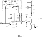
- the radio frequency power amplifier provided by the present embodiment includes two stages of amplifier circuits, a first bias circuit and a power detection feedback circuit, wherein in the two stages of amplifier circuits, each stage of amplifier circuit uses a common emitter amplifier circuit, i.e., a radio frequency input signal is input into a base of a transistor 101 of a first stage of amplifier circuit through a direct current blocking capacitor. An emitter of the transistor 101 is grounded. An inductor 102, serving as the load of the first stage of amplifier circuit, is connected between a collector of the transistor 101 and the power supply voltage.
- the output power of the first stage of amplifier circuit respectively enters bases of a transistor 105a, a transistor 105b and a transistor 105c of a second stage of amplifier circuit through the collector of the transistor 101 and a capacitor 103a, a capacitor 103b and a capacitor 103c. Emitters of the transistor 105a, the transistor 105b and the transistor 105c of the second stage of amplifier circuit are jointly grounded.
- An inductor 106 is used as a load of the second stage of amplifier circuit. One end of the inductor 106 is connected to the power supply voltage, and the other end of the inductor 106 is respectively connected to collectors of the transistor 105a, the transistor 105b and the transistor 105c.
- the output power of the second stage of amplifier circuit is transmitted to the output end to be output through the direct current blocking capacitor after passing through the collectors of the transistor 105a, the transistor 105b and the transistor 105c.
- the first bias circuit includes a transistor 110, a resistor 107, a diode 108 and a diode 109.
- a collector of the transistor 110 is respectively connected to a bias voltage Vbias and one end of the resistor 107.
- the other end of the resistor 107 is respectively connected to a base of the transistor 110 and an anode of the triode 108.
- a cathode of the diode 108 is connected to an anode of the diode 109.
- a cathode of the diode 109 is grounded.
- An emitter of the transistor 110 is correspondingly connected to bases of the transistor 105a, the transistor 105b and the transistor 105c respectively through a resistor 104a, a resistor 104b and a resistor 104c.
- the bias voltage is provided for the transistor 105a, the transistor 105b and the transistor 105c of the second stage of amplifier circuit through the first bias circuit.
- a first resistor 112 and a first capacitor 111 are connected in series between the collector of the transistor 101 of the first stage of amplifier circuit and the base of a first transistor 115 of the power detection feedback circuit, wherein the first resistor 112 and the first capacitor 111 are connected in series to form a first detection circuit.
- the output power of the first stage of amplifier circuit is detected through the first resistor 112 and the first capacitor 111, and the intensity of the power leaked to the first transistor 115 can be controlled.
- a fourth resistor 116 and a fifth resistor 117 are correspondingly arranged among the collector of the first transistor 115, the power supply voltage and the base of a second transistor 118.
- the collector of the second transistor 118 is connected to the power supply voltage.
- the emitter of the second transistor 118 is connected to the base of the transistor 101 of the first stage of amplifier circuit through a resistor 119.
- the above-mentioned elements form a first feedback circuit.
- the bias voltage is provided for the base of the first transistor 115 through a second bias circuit.
- the second bias circuit includes a second resistor 113 and a third resistor 114. One end of the second resistor 113 and one end of the third resistor 114 are connected together to be used as the output end of the second bias circuit. The output end is connected to the base of the first transistor 115.
- the other end of the second resistor 113 is connected to the power supply voltage.
- the other end of the third resistor is grounded.
- the second resistor 113 and the third resistor 114 provide the bias voltage for the first transistor 115 through voltage dividing effects.
- the output power of the transistor 101 of the first stage of amplifier circuit is leaked to the base of the first transistor 115 through the first resistor 112 and the first capacitor 111, so that the operating current of the first transistor 115 is varied.
- the power leaked to the first transistor 115 through the first resistor 112 and the first capacitor 111 correspondingly increases, so that the operating current of the first transistor 115 correspondingly increases.
- the control voltage on the fourth resistor 116 connected to the collector of the first transistor 115 can increase, and the base voltage of the first transistor 115 decreases through the fifth resistor 117, so that the current flowing through the first transistor 115 is controlled to correspondingly decrease.
- the current output by the second transistor 118 is input into the base of the transistor 101 of the first stage of amplifier circuit by the resistor 119, thereby decreasing the quiescent operating current of the transistor 101 of the first stage of amplifier circuit, so that the gain of the first stage of amplifier circuit decreases, and the output power of the first stage of amplifier circuit decreases.
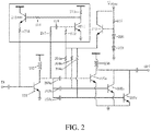
- the radio frequency power amplifier provided by the present embodiment includes two stages of amplifier circuits, a first bias circuit, a power detection feedback circuit and a current detection feedback circuit, wherein in the two stages of amplifier circuits, a first stage of amplifier circuit includes a transistor 201 and an inductor 202; a second stage of amplifier circuit includes a transistor 205a, a transistor 205b, a transistor 205c and an inductor 206; the first bias circuit includes a transistor 210, a resistor 207, a diode 208 and a diode 209; the structures of the first stage of amplifier circuit, the second stage of amplifier circuit and the first bias circuit are identical to those in Embodiment 1, and are not repeated herein.
- the output power of the first stage of amplifier circuit respectively enters the bases of the transistor 205a, the transistor 205b and the transistor 205c of the second stage of amplifier circuit through a collector of the transistor 201, a capacitor 203a, a capacitor 203b and a capacitor 203c.
- An emitter of the transistor 210 of the first bias circuit is correspondingly connected to bases of the transistor 205a, the transistor 205b and the transistor 205c respectively through a resistor 204a, a resistor 204b and a resistor 204c, and a bias voltage is provided for the transistor 205a, the transistor 205b and the transistor 205c of the second stage of amplifier circuit.
- the base of the transistor 211 (the transistor 211 equals to the first transistor 115 in Embodiment 1) is sequentially connected to a capacitor 218 and a resistor 217.
- the resistor 217 and the capacitor 218 are connected in series between the collector of the transistor 201 and the base of the transistor 211 of the first stage of amplifier circuit.
- the output power of the first stage of amplifier circuit is detected through the resistor 217 and the capacitor 218, and the intensity of the power leaked into the transistor 211 can be controlled, wherein the resistor 217 equals to the first resistor 112 in Embodiment 1, and the capacitor 218 equals to the first capacitor 111 in Embodiment 1, namely the resistor 217 and the capacitor 218 are connected in series to form the first detection circuit.
- the radio frequency power amplifier based on power detection feedback has input power, the output power of the transistor 201 of the first stage of amplifier circuit will be leaked to the base of the transistor 211 through the resistor 217 and the capacitor 218.
- the control voltage on a resistor 213 (the resistor 213 equals to the fourth resistor 116 in Embodiment 1) connected to the collector of the transistor 211 can also increase.
- the voltage of the base of a transistor 215 decreases through a resistor 214 (the resistor 214 equals to the fifth resistor 117 in Embodiment 1), so that the current flowing through the transistor 215 also correspondingly decreases.
- a current output from the transistor 215 is input into the base of the transistor 201 of the first stage of amplifier circuit through a resistor 216, thereby decreasing the quiescent operating current of the transistor 201 of the first stage of amplifier circuit, so that the gain of the first stage of amplifier circuit decreases, and the output power of the first stage of amplifier circuit decreases.
- the transistor 211, the transistor 215, the resistor 213 and the resistor 214 also form a first feedback circuit, and the connection relationship is identical to that in Embodiment 1.
- the base of the transistor 211 of the power detection feedback circuit of the radio frequency power amplifier provided by the present embodiment is connected to one end of a sixth resistor 212 (the sixth resistor forms the second detection circuit) to form a current detection feedback circuit.
- the other end of the sixth resistor 212 is respectively connected to the emitter of the transistor 210 of the first bias circuit, the resistor 204a, the resistor 204b and the resistor 204c, the bias voltage is provided for the transistor 211 through the first bias circuit, and the other end of the sixth resistor 212 is respectively connected to the bases of the transistor 205a, the transistor 205b and the transistor 205c of the second stage of amplifier circuit through the resistor 204a, the resistor 204b and the resistor 204c.
- the sixth resistor 212 and the transistor 211 form a mirror image of the resistor 204a, the resistor 204b, the resistor 204c and the transistor 205a, the transistor 205b, the transistor 205c.
- the transistor 211 can proportionally copy the quiescent operating currents of the transistor 205a, the transistor 205b and the transistor 205c.
- the gain of the radio frequency power amplifier based on power detection feedback correspondingly decreases.
- the quiescent operating currents of the transistor 205a, the transistor 205b and the transistor 205c copied on the transistor 211 of the current detection feedback circuit correspondingly decreases, so that the control voltage on the resistor 213 connected to the collector of the transistor 211 decreases.
- the control voltage of the base of the transistor 215 increases through the resistor 214, so that the current flowing through the transistor 215 is controlled to correspondingly increase.
- the current output by the transistor 215 is input into the base of the transistor 201 of the first stage of amplifier circuit through the resistor 216, so that the quiescent operating current of the transistor 201 of the first stage of amplifier circuit increases.
- the quiescent operating current on the first stage of amplifier circuit increases, and the gain of the radio frequency power amplifier based on power detection feedback correspondingly increases, thereby solving the problem of gain decrease of the radio frequency power amplifier based on power detection feedback caused by a decrease in the quiescent operating current of the second stage of amplifier circuit, and ensuring the total gain constancy of the radio frequency power amplifier based on power detection feedback.
- the radio frequency power amplifier based on power detection feedback can detect the output power of the first stage of amplifier circuit through the power defection feedback circuit, and can control the quiescent current of the first stage of amplifier circuit according to the detected output power of the first stage of amplifier circuit.
- the quiescent operating current of the input end of the second stage of amplifier circuit can be detected through the current detection feedback circuit, and the quiescent operating current of the first stage of amplifier circuit is controlled according to the detected quiescent operating current of the second stage of amplifier circuit, so that the radio frequency power amplifier operates in a state in which the gain and the output power are stable.
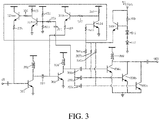
- the radio frequency power amplifier provided by the present embodiment includes three stages of amplifier circuits, a first bias circuit, a current detection feedback circuit and a power detection feedback circuit
- a first stage of amplifier circuit includes a transistor 301 and an inductor 302
- a second stage of amplifier circuit includes a transistor 304 and an inductor 305
- a third stage of amplifier circuit includes a transistor 308a, a transistor 308b, a transistor 308c and an inductor 309.
- the first bias circuit includes a transistor 313, a resistor 310, a diode 311 and a diode 312.
- the structures of the first stage of amplifier circuit and the second stage of amplifier circuit are identical to the structure of the first stage of amplifier circuit in Embodiment 1, the structure of the third stage of amplifier circuit is identical to the structure of the second stage of amplifier circuit in Embodiment 1, and the structures are not repeated herein.
- the structure of the first bias circuit is identical to the structure of the first bias circuit in Embodiment 1, and is not repeated herein.
- the output power of the first stage of amplifier circuit enters a base of the transistor 304 of the second stage of amplifier circuit through a collector of the transistor 301 and the capacitor 303.
- the output power of the second stage of amplifier circuit respectively enters bases of the transistor 308a, the transistor 308b and the transistor 308c through a collector of the transistor 304 and a capacitor 306a, a capacitor 306b and a capacitor 306c.
- An emitter of the transistor 313 of the first bias circuit is correspondingly connected to bases of the transistor 308a, the transistor 308b and the transistor 308c respectively through a resistor 307a, a resistor 307b and a resistor 307c, and the bias voltage is provided for the transistor 308a, the transistor 308b and the transistor 308c of the third stage of amplifier circuit.
- the power detection feedback circuit connects a resistor 320 and a capacitor 321 in series (for forming the first detection circuit) between the collector of the transistor 304 of the second stage of amplifier circuit and the base of a transistor 324 of the power detection feedback circuit, the output power of the second stage of amplifier circuit is detected through the resistor 320 and the capacitor 321, and the intensity of the power leaked to the transistor 324 can be controlled.
- the base of the transistor 324 is respectively connected to one end of a resistor 322 and one end of a resistor 323 (forming the second bias circuit), the other end of the resistor 322 is connected to the power supply voltage, and the other end of the resistor 323 is grounded.
- the resistor 322 and the resistor 323 provide the bias voltage for the transistor 324 through the voltage dividing effect.
- a resistor 325 and a resistor 326 are correspondingly arranged among the collector of the transistor 324, the power supply voltage and the base of a transistor 327.
- the collector of the transistor 327 is connected to the power supply voltage.
- the emitter of the transistor 327 is connected to the base of the transistor 301 of the first stage of amplifier circuit through a resistor 328.
- the transistor 324, the transistor 327, the resistor 325 and the resistor 326 form the first feedback circuit, wherein the resistor 320 equals to the first resistor 112 in Embodiment 1, the capacitor 321 equals to the first capacitor 111 in Embodiment 1, the transistor 324 equals to the first transistor 115 in Embodiment 1, the resistor 322 equals to the second resistor 113 in Embodiment 1, the resistor 323 equals to the third resistor 114 in Embodiment 1, the resistor 325 equals to the fourth resistor 116 in Embodiment 1, the resistor 326 equals to the fifth resistor 117 in Embodiment 1, and the transistor 327 equals to the second transistor 118 in Embodiment 1.
- the output power of the transistor 304 of the second stage of amplifier circuit will be leaked to the base of the transistor 324 through the resistor 320 and the capacitor 321, so that the operating current of the transistor 324 is varied.
- the resistor 325 generates a corresponding control voltage according to the operating current fed back by the collector of the transistor 324, the current flowing through the transistor 327 is controlled through the resistor 326, the current of the output end of the transistor 327 is input into the base of the transistor 301 of the first stage of amplifier circuit through the resistor 328, thereby controlling the quiescent operating current of the first stage of amplifier circuit, and ensuring the radio frequency power amplifier based on power detection feedback to operate in a state in which the gain and the output power are stable.
- a transistor 314, a transistor 319, a resistor 315 and a resistor 317 form the second feedback circuit, wherein the connection relationship among all elements in the second feedback circuit is identical to that of the first feedback circuit in Embodiment 1, and is not repeated herein.
- the resistor 316 equals to the sixth resistor in Embodiment 2, and identically forms the second detection circuit.
- the base of the transistor 314 is respectively connected to a resistor 307a, a resistor 307b and a resistor 307c through the resistor 316.
- the collector of the transistor 319 is connected to the power supply voltage.
- the emitter of the transistor 319 is connected to the base of the transistor 304 through the resistor 318.
- the resistor 316 and the transistor 314 form the mirror image of the resistor 307a, the resistor 307b, the resistor 307c and the transistor 308a, the transistor 308b, the transistor 308c, the transistor 314 can proportionally copy the quiescent operating currents of the transistor 308a, the transistor 308b and the transistor 308c by designing the proportion of the resistor 316 to the resistor 307a, the resistor 307b and the resistor 307c and the proportion of the transistor 314 to the transistor 308a, the transistor 308b and the transistor 308c.
- the radio frequency power amplifier can detect the quiescent operating current of the input end of the third stage of amplifier circuit through the resistor 316 (the second detection circuit), and can feed back the result to the resistor 315 through the collector of the transistor 314 after the quiescent operating current is copied through the transistor 314.
- the resistor 315 generates the corresponding control voltage according to the quiescent operating current, the current flowing through the transistor 319 is controlled through the resistor 317, different current flowing through the transistor 319 is input into the input end of the second stage of amplifier circuit through the resistor 318, thereby controlling the quiescent operating current of the second stage of amplifier circuit, and ensuring the second stage of amplifier circuit to operate in a state in which the gain is stable.
- the radio frequency power amplifier provided by the present embodiment can detect the output power of the second stage of amplifier circuit through the power detection feedback circuit, and can control the quiescent current of the first stage of amplifier circuit according to the detected output power of the second stage of amplifier circuit.
- the quiescent operating current of the input end of the third stage of amplifier circuit can also be detected through the current detection feedback circuit, and the quiescent operating current of the second stage of amplifier circuit is controlled according to the detected quiescent operating current of the input end of the third stage of amplifier circuit, so that the radio frequency power amplifier based on power detection feedback operates in a state in which the gain and the output power are stable.
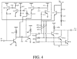
- the radio frequency power amplifier provided by the present embodiment includes three stages of amplifier circuits, a first bias circuit, a current detection feedback circuit and a power detection feedback circuit.
- a first stage of amplifier circuit includes a transistor 401 and an inductor 402;
- a second stage of amplifier circuit includes a transistor 405 and an inductor 404;
- a third stage of amplifier circuit includes a transistor 408a, a transistor 408b, a transistor 408c and an inductor 409.
- the first bias circuit includes a transistor 413, a resistor 410, a diode 411 and a diode 412.
- the structures of the first stage of amplifier circuit, the second stage of amplifier circuit and the third stage of amplifier circuit are identical to the structures of the first stage of amplifier circuit, the second stage of amplifier circuit and the third stage of amplifier circuit in Embodiment 3, the structure of the first bias circuit is identical to the structure of the first bias circuit in Embodiment 1, and are not repeated herein.
- the output power of the first stage of amplifier circuit enters the base of the transistor 405 of the second stage of amplifier circuit through a collector of the transistor 401 and the capacitor 403, the output power of the second stage of amplifier circuit respectively enters bases of the transistor 408a, the transistor 408b and the transistor 408c of the third stage of amplifier circuit through the collector of the transistor 405, a capacitor 406a, a capacitor 406b and a capacitor 406c.
- the emitter of the transistor 413 of the first bias circuit is respectively connected to the bases of the transistor 408a, the transistor 408b and the transistor 408c through a resistor 407a, a resistor 407b and a resistor 407c, and the bias voltage is provided for the transistor 408a, the transistor 408b and the transistor 408c of the third stage of amplifier circuit.
- the power detection feedback circuit connects a resistor 420 and a capacitor 421 in series (the resistor 420 and the capacitor 421 are connected in series to form the first detection circuit) between the collector of the transistor 401 of the first stage of amplifier circuit and the base of a transistor 424 of the power detection feedback circuit.
- the output power of the first stage of amplifier circuit is detected through the resistor 420 and the capacitor 421, and the intensity of the power leaked into the transistor 424 can be controlled.
- the power detection feedback circuit provides the bias voltage for the transistor 424 through the voltage dividing effect of a resistor 422 and a resistor 423 (the resistor 422 and the resistor 423 form the second bias circuit).
- the output power of the transistor 401 of the first stage of amplifier circuit will be leaked to the base of the transistor 424 through the resistor 420 and the capacitor 421, so that the operating current of the transistor 424 is varied.
- a resistor 425 generates the corresponding control voltage according to the operating current fed back by the collector of the transistor 424.
- the current flowing through a transistor 427 is controlled through a resistor 426, and the current of the output end of the transistor 427 is input into the base of the transistor 401 of the first stage of amplifier circuit through a resistor 428, thereby controlling the quiescent operating current of the first stage of amplifier circuit, and ensuring the radio frequency power amplifier based on power detection feedback to operate in a state in which the gain and the output power are stable.
- the current detection feedback circuit includes a second feedback circuit consisting of a transistor 414, a transistor 419, a resistor 415 and a resistor 417, and also includes a second detection circuit consisting of a resistor 416.
- the power detection feedback circuit includes a first feedback circuit consisting of the transistor 424, the transistor 427, the resistor 425 and the resistor 426, further includes a second bias circuit consisting of the resistor 422 and the resistor 423, and further includes a first detection circuit consisting of the resistor 420 and the capacitor 421, wherein the structures of the first feedback circuit and the second feedback circuit are identical to the structure of the first feedback circuit in Embodiment 1, the structure of the first detection circuit is identical to that in Embodiment 1, the structure of the second detection circuit is identical to that in Embodiment 2, the structure of the second bias circuit is identical to that in Embodiment 1, and those structures are not repeated herein.
- the resistor 416 and the transistor 414 form a mirror image of the resistor 407a, the resistor 407b, the resistor 407c and the transistor 408a, the transistor 408b, the transistor 408c.
- the transistor 414 can proportionally copy the quiescent operating currents of the transistor 408a, the transistor 408b and the transistor 408c.
- the current detection feedback circuit detects the quiescent operating current of the third stage of amplifier circuit through the resistor 416, copies the quiescent operating current through the transistor 414, and then feeds back the result to the resistor 415 through the collector of the transistor 414.
- the resistor 415 generates the corresponding control voltage according to the quiescent operating current, and controls the current flowing through the transistor 419 through the resistor 417. Different current flowing through the transistor 419 is input into the second stage of amplifier circuit through the resistor 418, thereby controlling the quiescent operating current of the second stage of amplifier circuit, and ensuring the second stage of amplifier circuit to operate in a state in which the gain is stable.
- the radio frequency power amplifier provided by the present embodiment can detect the output power of the first stage of amplifier circuit through the power detection feedback circuit, and controls the quiescent current of the first stage of amplifier circuit according to the detected output power of the first stage of amplifier circuit.
- the radio frequency power amplifier provided by the present embodiment can also detect the quiescent operating current of the input end of the third stage of amplifier circuit through the current detection feedback circuit, and controls the quiescent operating current of the second stage of amplifier circuit according to the detected quiescent operating current of the third stage of amplifier circuit, so that the radio frequency power amplifier based on power detection feedback operates in a state in which the gain and the output power are stable.
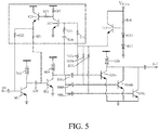
- the radio frequency power amplifier provided by the present embodiment includes three stages of amplifier circuits, a first bias circuit, a current detection feedback circuit and a power detection feedback circuit.
- a first stage of amplifier circuit includes a transistor 501 and an inductor 502;
- a second stage of amplifier circuit includes a transistor 505 and an inductor 504;
- a third stage of amplifier circuit includes a transistor 508a, a transistor 508b, a transistor 508c and an inductor 509.
- the first bias circuit includes a transistor 513, a resistor 510, a diode 511 and a diode 512.
- the structures of the first stage of amplifier circuit, the second stage of amplifier circuit and the third stage of amplifier circuit are identical to the structures of the first stage of amplifier circuit, the second stage of amplifier circuit and the third stage of amplifier circuit in Embodiment 3, the structure of the first bias circuit is identical to the structure of the first bias circuit in Embodiment 1, and are not repeated herein.
- the output power of the first stage of amplifier circuit enters a base of the transistor 505 of the second stage of amplifier circuit through a collector of the transistor 501 and a capacitor 503, the output power of the second stage of amplifier circuit respectively enters bases of the transistor 508a, the transistor 508b and the transistor 508c of the third stage of amplifier circuit through the collector of the transistor 505, a capacitor 506a, a capacitor 506b and a capacitor 506c.
- An emitter of the transistor 513 of the first bias circuit is correspondingly and respectively connected to the bases of the transistor 508a, the transistor 508b and the transistor 508b through a resistor 507a, a resistor 507b and a resistor 507c, and the bias voltage is provided for the transistor 508a, the transistor 508b and the transistor 508c of the third stage of amplifier circuit.
- the base of a transistor 517 (the transistor 517 equals to the first transistor 115 in Embodiment 1) is sequentially connected to a resistor 515 and a capacitor 516, and the resistor 515 and the capacitor 516 are connected in series between the collector of the transistor 505 of the second stage of amplifier circuit and the base of the transistor 517.
- the output power of the second stage of amplifier circuit is detected through the resistor 515 and the capacitor 516, and the intensity of the power leaked to the transistor 517 can be controlled, wherein the resistor 515 equals to the first resistor 112 in Embodiment 1, and the capacitor 516 equals to the first capacitor 111 in Embodiment 1.
- the output power of the transistor 505 of the second stage of amplifier circuit will be leaked to the base of the transistor 517 through the resistor 515 and the capacitor 516, so that the operating current of the transistor 517 is varied.
- a resistor 518 (equals to the fourth resistor 116 in Embodiment 1) generates the corresponding control voltage according to the operating current fed back by the collector of the transistor 517.
- the current flowing through a transistor 520 (equals to the second transistor 118 in Embodiment 1) is controlled through a resistor 519 (equals to the fifth resistor 117 in Embodiment 1), the current of the output end of the transistor 520 is respectively input to the base of the transistor 501 of the first stage of amplifier circuit and the base of the transistor 505 of the second stage of amplifier circuit through a resistor 521 and a resistor 522, thereby controlling the quiescent operating current of the first stage of amplifier circuit and the second stage of amplifier circuit, and ensuring the radio frequency power amplifier based on power detection feedback to operate in a state in which the gain and the output power are stable.
- the radio frequency power amplifier provided by the present embodiment can detect the output power of the second stage of amplifier circuit through the power detection feedback circuit, and respectively controls the quiescent current of the first stage of amplifier circuit and the second stage of amplifier circuit according to the detected output power of the second stage of amplifier circuit.
- the radio frequency power amplifier provided by the present embodiment can also detect the quiescent operating current of the input end of the third stage of amplifier circuit through the current detection feedback circuit, and respectively controls the quiescent operating current of the first stage of amplifier circuit and the second stage of amplifier circuit according to the detected quiescent operating current of the third stage of amplifier circuit, so that the radio frequency power amplifier based on power detection feedback operates in a state in which the gain and the output power are stable.
- a resistor 514 (equals to the sixth resistor 212 in Embodiment 2) is connected to the base of the transistor 517 of the power detection feedback circuit provided by the present embodiment, and a current detection feedback circuit is formed.
- the structure of the current detection feedback circuit provided by the present embodiment is characterized in that the current detection feedback circuit uses the resistor 521 and the resistor 522 for correspondingly connecting the base of the transistor 505 of the second stage of amplifier circuit and the base of the transistor 501 of the first stage of amplifier circuit, the current output by the transistor 520 is respectively input into the first stage of amplifier circuit and the second stage of amplifier circuit, thereby controlling the quiescent operating current of the first stage of amplifier circuit and the second stage of amplifier circuit.
- the current detection feedback circuit detects the quiescent operating current of the third stage of amplifier circuit through the resistor 514, copies the quiescent operating current through the transistor 517 and then feeds back the result to the resistor 518 through the collector of the transistor 517.
- the resistor 518 generates a corresponding control voltage according to the quiescent operating current, and controls the current flowing through the transistor 520 through the resistor 519, different current flowing through the transistor 520 is respectively input into the first stage of amplifier circuit and the second stage of amplifier circuit through the resistor 521 and the resistor 522, thereby controlling the quiescent operating currents of the first stage of amplifier circuit and the second stage of amplifier circuit, and ensuring the radio frequency power amplifier based on power detection feedback to operate in a state in which the gain is stable.
- the power detection feedback circuit can also use a capacitor to replace a structure of connecting a capacitor and a resistor in series to be connected between the output end of the current stage of amplifier circuit and the input end of the power detection feedback circuit, and the output power of the current stage of amplifier circuit is detected through the capacitor.
- the operating principle of the power detection feedback circuit is as mentioned above and is not repeated herein. It should be noted that the transistors in the first bias circuit, the power detection feedback circuit and the current detection feedback circuit in the radio frequency power amplifier provided by the present invention are bipolar transistors.
- the radio frequency power amplifier provided by the present invention can connect the input end of the power detection feedback circuit to the output end of the current stage of amplifier circuit of the radio frequency power amplifier based on power detection feedback, and can also connect the input end of a certain stage of amplifier circuit located posterior to the current stage of amplifier circuit connected to the power detection feedback circuit to the input end of the current detection feedback circuit after connecting the input end of the power detection feedback circuit to the output end of the current stage of amplifier circuit of the radio frequency power amplifier based on power detection feedback.
- the radio frequency power amplifier achieves the following effects that:
- the radio frequency power amplifier can effectively inhibit the operating state variation of the radio frequency power amplifier caused by the process variation, and can reduce the influence of the variation of an input signal on the operating state of the radio frequency power amplifier, so that the radio frequency power amplifier operates in a state in which the gain and the output power are stable.
- the radio frequency power amplifier provided by the present invention can be used in a radio frequency chip. Concrete structures of the radio frequency power amplifier based on power detection feedback in the radio frequency chip are not illuminated one by one in detail herein.
- the radio frequency power amplifier based on power detection feedback can also be used in a communication terminal to be used as an important composition part of a radio frequency integrated circuit.
- the communication terminal mentioned herein refers to computer equipment capable of being used in a mobile environment and supporting various communication systems such as GSM, EDGE, TD_SCDMA, TDD_LTE and FDD_LTE, including a mobile phone, a notebook computer, a tablet personnel computer, a car computer, etc.
- the technical scheme provided by the present invention is also applicable to other occasions of radio frequency integrated circuit application, such as communication base stations.
Landscapes
- Engineering & Computer Science (AREA)
- Power Engineering (AREA)
- Microelectronics & Electronic Packaging (AREA)
- Amplifiers (AREA)
Abstract
Description
- The present invention relates to a radio frequency power amplifier, in particular to a radio frequency power amplifier based on power detection feedback, also relates to a chip including the radio frequency power amplifier and a corresponding communication terminal, and belongs to the technical field of radio frequency integrated circuits.
- At present, the development of wireless communication greatly satisfies the requirements of people on communication, and those requirements further drive wireless communication terminals to fast increase all over the world. A radio power amplifier is a necessary function module in the wireless communication terminal, and has a main effect of amplifying the emission power of the communication terminal so as to still maintain a sufficient signal intensity when a signal reaches a base station, so that the lowest signal-to-noise ratio required for communication is realized, and the signal sending and receiving operation of a whole communication link is completed.
- In a wireless communication system, the main direct current power consumption is from a radio frequency power amplifier, and the operating time of the system can be obviously prolonged by reducing the power consumption of the radio frequency power amplifier. On the other hand, the integral performance of a radio frequency circuit is directly determined by the performance of the radio frequency power amplifier. In addition, the design of the radio frequency power amplifier generally requires stable gain and output power.
- However, in realization of the radio frequency power amplifier, due to the influence of factors such as process deviation and temperature variation, the gain and the output power of the radio frequency power amplifier vary in a large range. Meanwhile, by considering that the amplitude of an input signal is influenced by the process deviation and the temperature variation, the variation of the input signal can cause the output power of the radio frequency power amplifier to vary in a larger range. Therefore, feedback control needs to be performed on the quiescent operating current and the output power of the radio frequency power amplifier, so that the operating state variation of the radio frequency power amplifier caused by process variation is inhibited, the influence of variation of the input signal on the operating state of the radio frequency power amplifier can be reduced, so that the radio frequency power amplifier operates in a state in which the gain and the output power are stable.
- The primary technical problem to be solved by the present invention is to provide a radio frequency power amplifier based on power detection feedback.
- Another technical problem to be solved by the present invention is to provide a chip including the radio frequency power amplifier and a corresponding communication terminal.
- In order to achieve the goals, the present invention adopts the following technical schemes:
According to a first aspect of embodiments of the present invention, a radio frequency power amplifier based on power detection feedback is provided. The radio frequency power amplifier based on power detection feedback includes multiple stages of amplifier circuits and at least one power detection feedback circuit. An input end of the power detection feedback circuit is connected to an output end of a current stage of amplifier circuit in the multiple stages of amplifier circuits. An output end of the power detection feedback circuit is connected to input ends of the current stage of amplifier circuit and at least one stage of amplifier circuit located prior to the current stage of amplifier circuit. - The power detection feedback circuit generates, according to the detected output power of the current stage of amplifier circuit, a control voltage varying inversely with the output power, so that the power detection feedback circuit outputs a current varying positively with the control voltage. The current is input into the input ends of the current stage of amplifier circuit and the at least one stage of amplifier circuit located prior to the current stage of amplifier circuit, and a quiescent operating current of at least one stage of amplifier circuit varies positively with the current, so that the radio frequency power amplifier operates in a state in which the gain and the output power are stable.
- Preferably, the radio frequency power amplifier further includes at least one current detection feedback circuit, wherein an input end of the current detection feedback circuit is connected to an input end of a certain stage of amplifier circuit located posterior to the current stage of amplifier circuit through a corresponding resistor. An output end of the current detection feedback circuit is connected to an input end of at least one stage of amplifier circuit located prior to the current stage of amplifier circuit.
- The current detection feedback circuit generates, according to a detected quiescent operating current of the current stage of amplifier circuit, a control voltage varying inversely with the quiescent operating current, so that the current detection feedback circuit outputs a current varying positively with the control voltage. The current is input into the input end of the at least one stage of amplifier circuit located prior to the current stage of amplifier circuit, so that the quiescent operating current of at least one stage of amplifier circuit varies positively with the current. The radio frequency power amplifier operates in a state in which the gain and the output power are stable.
- Preferably, the power detection feedback circuit includes a first detection circuit and a first feedback circuit, wherein an output end of the first detection circuit is connected to an input end of the first feedback circuit. An input end of the first detection circuit is connected to the output end of the current stage of amplifier circuit. An output end of the first feedback circuit is connected to the input ends of the current stage of amplifier circuit and the at least one stage of amplifier circuit located prior to the current stage of amplifier circuit.
- Preferably, the input end of the first feedback circuit is connected to an output end of a second detection circuit. The detected quiescent operating current of the current stage of amplifier circuit is input into the first feedback circuit through the second detection circuit.
- Preferably, the current detection feedback circuit includes a second detection circuit and a second feedback circuit, wherein an output end of the second detection circuit is connected to an input end of the second feedback circuit. An input end of the second detection circuit is connected to the input end of the current stage of amplifier circuit. An output end of the second feedback circuit is connected to the input end of the at least one stage of amplifier circuit located prior to the current stage of amplifier circuit.
- Preferably, the first detection circuit is formed by connecting a first resistor and a first capacitor in series. The second detection circuit consists of a sixth resistor.
- Preferably, the first detection circuit consists of the first capacitor.
- Preferably, each of the first feedback circuit and the second feedback circuit includes two transistors, wherein a fourth resistor is arranged between a collector of a first transistor and a power supply voltage. A fifth resistor is arranged between the collector of the first transistor and a base of a second transistor. A collector of the second transistor is connected to the power supply voltage. A base of the first transistor is used as the input end of the feedback circuit. An emitter of the second transistor is used as the output end of the feedback circuit.
- Preferably, when the current detection feedback circuit shares the first feedback circuit with the power detection feedback circuit, a bias voltage is respectively provided for the current stage of amplifier circuit and the first transistor through a first basis circuit. The first bias circuit includes a transistor. A collector of the transistor is connected to the bias voltage. An emitter of the transistor is connected to the base of the first transistor through the sixth resistor. The emitter of the transistor is connected to the input end of the current stage of amplifier circuit. A resistor is arranged between the base of the transistor and the bias voltage. Two diodes are connected in series between the base of the transistor and a ground wire.
- Preferably, the bias voltage is provided for the first transistor of the power detection feedback circuit through a second bias circuit. The second bias circuit includes a second resistor and a third resistor. One end of the second resistor is connected to the power supply voltage. The other end of the second resistor and one end of the third resistor are connected together to form the output end of the second bias circuit. The other end of the third resistor is grounded.
- Preferably, the bias voltage is respectively provided for the first transistor of the current detection feedback circuit and the current stage of amplifier circuit through the first bias circuit.
- Preferably, in multiple stages of amplifier circuits, each stage of amplifier circuit is a common emitter amplifier circuit consisting of a bipolar transistor or a CMOS transistor. A load is arranged between each stage of amplifier circuit and the power supply voltage. The load is a resistor or an inductor. A capacitor is arranged between an input end of a posterior stage of amplifier circuit and an output end of a prior stage of amplifier circuit.
- According to a second aspect of the embodiments of the present invention, a chip is provided, wherein the chip includes the radio frequency power amplifier based on power detection feedback.
- According to a third aspect of the embodiments of the present invention, a communication terminal is provided, wherein the communication terminal includes the radio frequency power amplifier based on power detection feedback.
- The radio frequency power amplifier provided by the present invention is used for realizing the detection of the output power of the current stage of amplifier current through arranging the power detection feedback circuit, generating a control voltage varying inversely with the output power according to the detected output power, and enabling the power detection feedback circuit to output current varying positively with the control voltage. The current is input into the input ends of the current stage of amplifier circuit and at least one stage of amplifier circuit located prior to the current stage of amplifier circuit through the power detection feedback circuit, and the quiescent operating currents of the current stage of amplifier circuit and the at least one stage of amplifier circuit located prior to the current stage of amplifier circuit is controlled, so that the radio frequency power amplifier operates in a state in which the gain and the output power are stable.
-
-
Fig. 1 is a circuit schematic diagram of a radio frequency power amplifier based on power detection feedback provided by Embodiment 1 of the present invention. -
Fig. 2 is a circuit schematic diagram of a radio frequency power amplifier based on power detection feedback provided by Embodiment 2 of the present invention. -
Fig. 3 is a circuit schematic diagram of a radio frequency power amplifier based on power detection feedback provided by Embodiment 3 of the present invention. -
Fig. 4 is a circuit schematic diagram of a radio frequency power amplifier based on power detection feedback provided by Embodiment 4 of the present invention. -
Fig. 5 is a circuit schematic diagram of a radio frequency power amplifier based on power detection feedback provided by Embodiment 5 of the present invention. - The following further describes the technical content of the present disclosure with reference to the accompanying drawings and specific embodiments.
- A radio frequency power amplifier provided by the present invention includes multiple stages of amplifier circuits, a first bias circuit and a detection feedback circuit, wherein the multiple stages of amplifier circuits are connected to the first bias circuit, and the first bias circuit provides a bias voltage for the multiple stages of amplifier circuits. The detection feedback circuit includes at least one power detection feedback circuit, or the detection feedback circuit includes at least one power detection feedback circuit and current detection feedback circuit. Each power detection feedback circuit and each current detection feedback current are respectively connected to the multiple stages of amplifier circuits, wherein when the output power of the current stage of amplifier circuit increases or decreases, the output power of the radio frequency power amplifier based on power detection feedback correspondingly increases or decreases. At the moment, the output power of the current stage of amplifier circuit detected by the power detection feedback circuit connected to the current stage of amplifier circuit accordingly increases or decreases, a corresponding current is generated according to the output power, and at the same time, a corresponding control voltage is generated according to the current. The power detection feedback circuit correspondingly decreases or increases the control voltage, so that current output by the power detection feedback circuit correspondingly decreases or increases. The current output by the power detection feedback circuit can be input into the input end of the current stage of amplifier circuit and at least one stage of amplifier circuit located prior to the current stage of amplifier circuit, so that the quiescent operating currents of the current stage of amplifier circuit and the at least one stage of amplifier circuit located prior to the current stage of amplifier circuit correspondingly decrease or increase, and the gain and output power of the current stage of amplifier circuit and the at least one stage of amplifier circuit located prior to the current stage of amplifier circuit correspondingly decrease or increase, so that the problem of gain and output power increase or decrease of the radio frequency power amplifier caused by output power increase or decrease of the current stage of amplifier circuit can be solved, thereby effectively inhibiting the operating state variation of the radio frequency power amplifier caused by the process variation, and reducing the influence on the operating state of the radio frequency power amplifier caused by variation of an input signal, so that the radio frequency power amplifier operates in a state in which the gain and the output power are stable.
- When a quiescent operating current of an input end of a certain stage of amplifier circuit located posterior to the current stage of amplifier circuit increases or decreases for certain reasons (such as variation of the production process), the gain of the radio frequency power amplifier based on power detection feedback correspondingly increases or decreases. At the moment, the quiescent operating current of the input end of the certain stage of amplifier circuit detected and copied by the current detection feedback circuit connected to the certain stage of amplifier circuit accordingly increases or decreases, the control voltage generated by the current detection feedback circuit according to the increased or decreased quiescent operating current correspondingly decreases or increases, and the current output by the current detection feedback circuit correspondingly decreases or increases through the decreased or increased control voltage. The current output by the current detection feedback circuit is input into the input end of at least one stage of amplifier circuit located prior to the certain stage of amplifier circuit, so that the quiescent operating current of the input end of the at least one stage of amplifier circuit located prior to the certain stage of amplifier circuit accordingly decreases or increases, the gain of at least one stage of amplifier circuit located prior to the certain stage of amplifier circuit accordingly increases or decreases, thereby solving the problem of gain increase or decrease of the radio frequency power amplifier based on power detection feedback caused by an increase or decrease in the quiescent operating current of the certain stage of amplifier circuit, and ensuring the total gain constancy of the radio frequency power amplifier based on power detection feedback.
- In the radio frequency power amplifier provided by the present invention, the position relationship between each stage of amplifier circuit in the multiple stages of amplifier circuits uses the current flowing direction of the multiple stages of amplifier circuits as a reference, namely the front and back position relationships mentioned in various parts in the present invention all use the current flowing direction of the multiple stages of amplifier circuits as the reference.
- It should be noted that in the radio frequency power amplifier provided by the present invention, the current output by the power detection feedback circuit is input into the input ends of the current stage of amplifier circuit and at least one stage of amplifier circuit located prior to the current stage of amplifier circuit, wherein the at least one stage of amplifier circuit includes a condition of any one stage or multiple stages of amplifier circuits, and the at least one stage of amplifier circuit includes a condition of the current stage of amplifier circuit. The current output by the current detection feedback circuit can be input into the input end of at least one stage of amplifier circuit located prior to the certain stage of amplifier circuit, wherein the at least one stage of amplifier circuit includes the condition of any one stage or multiple stages of amplifier circuits, but the at least one stage of amplifier circuit does not include the certain stage of amplifier circuit.
- In the radio frequency power amplifier provided by the present invention, each stage of amplifier circuit can consist of a bipolar transistor or a CMOS transistor, and a resistor or an inductor can be arranged between each stage of amplifier circuit and the power supply voltage to be used as a load. A structure and an operating principle of the radio frequency power amplifier provided by the present invention will be illustrated in detail hereafter with reference to
Fig. 1-Fig. 5 , using two stages of amplifier circuits and three stages of amplifier circuits consisting of the bipolar transistor (called as transistor for short hereafter) and using the inductor as the load of each stage of amplifier circuit. - As shown in
Fig. 1 , the radio frequency power amplifier provided by the present embodiment includes two stages of amplifier circuits, a first bias circuit and a power detection feedback circuit, wherein in the two stages of amplifier circuits, each stage of amplifier circuit uses a common emitter amplifier circuit, i.e., a radio frequency input signal is input into a base of atransistor 101 of a first stage of amplifier circuit through a direct current blocking capacitor. An emitter of thetransistor 101 is grounded. Aninductor 102, serving as the load of the first stage of amplifier circuit, is connected between a collector of thetransistor 101 and the power supply voltage. The output power of the first stage of amplifier circuit respectively enters bases of atransistor 105a, atransistor 105b and atransistor 105c of a second stage of amplifier circuit through the collector of thetransistor 101 and acapacitor 103a, acapacitor 103b and acapacitor 103c. Emitters of thetransistor 105a, thetransistor 105b and thetransistor 105c of the second stage of amplifier circuit are jointly grounded. Aninductor 106 is used as a load of the second stage of amplifier circuit. One end of theinductor 106 is connected to the power supply voltage, and the other end of theinductor 106 is respectively connected to collectors of thetransistor 105a, thetransistor 105b and thetransistor 105c. The output power of the second stage of amplifier circuit is transmitted to the output end to be output through the direct current blocking capacitor after passing through the collectors of thetransistor 105a, thetransistor 105b and thetransistor 105c. - The first bias circuit includes a
transistor 110, aresistor 107, adiode 108 and adiode 109. A collector of thetransistor 110 is respectively connected to a bias voltage Vbias and one end of theresistor 107. The other end of theresistor 107 is respectively connected to a base of thetransistor 110 and an anode of thetriode 108. A cathode of thediode 108 is connected to an anode of thediode 109. A cathode of thediode 109 is grounded. An emitter of thetransistor 110 is correspondingly connected to bases of thetransistor 105a, thetransistor 105b and thetransistor 105c respectively through aresistor 104a, aresistor 104b and aresistor 104c. The bias voltage is provided for thetransistor 105a, thetransistor 105b and thetransistor 105c of the second stage of amplifier circuit through the first bias circuit. - According to the power detection feedback circuit of the radio frequency power amplifier provided by the present embodiment, a
first resistor 112 and afirst capacitor 111 are connected in series between the collector of thetransistor 101 of the first stage of amplifier circuit and the base of afirst transistor 115 of the power detection feedback circuit, wherein thefirst resistor 112 and thefirst capacitor 111 are connected in series to form a first detection circuit. The output power of the first stage of amplifier circuit is detected through thefirst resistor 112 and thefirst capacitor 111, and the intensity of the power leaked to thefirst transistor 115 can be controlled. Afourth resistor 116 and afifth resistor 117 are correspondingly arranged among the collector of thefirst transistor 115, the power supply voltage and the base of asecond transistor 118. The collector of thesecond transistor 118 is connected to the power supply voltage. The emitter of thesecond transistor 118 is connected to the base of thetransistor 101 of the first stage of amplifier circuit through aresistor 119. The above-mentioned elements form a first feedback circuit. The bias voltage is provided for the base of thefirst transistor 115 through a second bias circuit. Concretely, the second bias circuit includes asecond resistor 113 and athird resistor 114. One end of thesecond resistor 113 and one end of thethird resistor 114 are connected together to be used as the output end of the second bias circuit. The output end is connected to the base of thefirst transistor 115. The other end of thesecond resistor 113 is connected to the power supply voltage. The other end of the third resistor is grounded. Thesecond resistor 113 and thethird resistor 114 provide the bias voltage for thefirst transistor 115 through voltage dividing effects. - When the radio frequency power amplifier has input power, the output power of the
transistor 101 of the first stage of amplifier circuit is leaked to the base of thefirst transistor 115 through thefirst resistor 112 and thefirst capacitor 111, so that the operating current of thefirst transistor 115 is varied. For example, when the output power of the first stage of amplifier circuit increases, the power leaked to thefirst transistor 115 through thefirst resistor 112 and thefirst capacitor 111 correspondingly increases, so that the operating current of thefirst transistor 115 correspondingly increases. At the moment, the control voltage on thefourth resistor 116 connected to the collector of thefirst transistor 115 can increase, and the base voltage of thefirst transistor 115 decreases through thefifth resistor 117, so that the current flowing through thefirst transistor 115 is controlled to correspondingly decrease. The current output by thesecond transistor 118 is input into the base of thetransistor 101 of the first stage of amplifier circuit by theresistor 119, thereby decreasing the quiescent operating current of thetransistor 101 of the first stage of amplifier circuit, so that the gain of the first stage of amplifier circuit decreases, and the output power of the first stage of amplifier circuit decreases. - As shown in
Fig. 2 , the radio frequency power amplifier provided by the present embodiment includes two stages of amplifier circuits, a first bias circuit, a power detection feedback circuit and a current detection feedback circuit, wherein in the two stages of amplifier circuits, a first stage of amplifier circuit includes atransistor 201 and aninductor 202; a second stage of amplifier circuit includes atransistor 205a, atransistor 205b, atransistor 205c and aninductor 206; the first bias circuit includes atransistor 210, aresistor 207, adiode 208 and adiode 209; the structures of the first stage of amplifier circuit, the second stage of amplifier circuit and the first bias circuit are identical to those in Embodiment 1, and are not repeated herein. Similarly, the output power of the first stage of amplifier circuit respectively enters the bases of thetransistor 205a, thetransistor 205b and thetransistor 205c of the second stage of amplifier circuit through a collector of thetransistor 201, acapacitor 203a, acapacitor 203b and acapacitor 203c. An emitter of thetransistor 210 of the first bias circuit is correspondingly connected to bases of thetransistor 205a, thetransistor 205b and thetransistor 205c respectively through aresistor 204a, aresistor 204b and aresistor 204c, and a bias voltage is provided for thetransistor 205a, thetransistor 205b and thetransistor 205c of the second stage of amplifier circuit. - In the power detection feedback circuit provided by the present embodiment, the base of the transistor 211 (the
transistor 211 equals to thefirst transistor 115 in Embodiment 1) is sequentially connected to acapacitor 218 and a resistor 217. The resistor 217 and thecapacitor 218 are connected in series between the collector of thetransistor 201 and the base of thetransistor 211 of the first stage of amplifier circuit. The output power of the first stage of amplifier circuit is detected through the resistor 217 and thecapacitor 218, and the intensity of the power leaked into thetransistor 211 can be controlled, wherein the resistor 217 equals to thefirst resistor 112 in Embodiment 1, and thecapacitor 218 equals to thefirst capacitor 111 in Embodiment 1, namely the resistor 217 and thecapacitor 218 are connected in series to form the first detection circuit. When the radio frequency power amplifier based on power detection feedback has input power, the output power of thetransistor 201 of the first stage of amplifier circuit will be leaked to the base of thetransistor 211 through the resistor 217 and thecapacitor 218. For example, when the output power of the first stage of amplifier circuit increases, the power leaked to thetransistor 211 through the resistor 217 and thecapacitor 218 correspondingly increase, so that the operating current of thetransistor 211 also correspondingly increases. At the moment, the control voltage on a resistor 213 (theresistor 213 equals to thefourth resistor 116 in Embodiment 1) connected to the collector of thetransistor 211 can also increase. The voltage of the base of atransistor 215 decreases through a resistor 214 (theresistor 214 equals to thefifth resistor 117 in Embodiment 1), so that the current flowing through thetransistor 215 also correspondingly decreases. A current output from thetransistor 215 is input into the base of thetransistor 201 of the first stage of amplifier circuit through aresistor 216, thereby decreasing the quiescent operating current of thetransistor 201 of the first stage of amplifier circuit, so that the gain of the first stage of amplifier circuit decreases, and the output power of the first stage of amplifier circuit decreases. It should be noted that thetransistor 211, thetransistor 215, theresistor 213 and theresistor 214 also form a first feedback circuit, and the connection relationship is identical to that in Embodiment 1. - The base of the
transistor 211 of the power detection feedback circuit of the radio frequency power amplifier provided by the present embodiment is connected to one end of a sixth resistor 212 (the sixth resistor forms the second detection circuit) to form a current detection feedback circuit. The other end of thesixth resistor 212 is respectively connected to the emitter of thetransistor 210 of the first bias circuit, theresistor 204a, theresistor 204b and theresistor 204c, the bias voltage is provided for thetransistor 211 through the first bias circuit, and the other end of thesixth resistor 212 is respectively connected to the bases of thetransistor 205a, thetransistor 205b and thetransistor 205c of the second stage of amplifier circuit through theresistor 204a, theresistor 204b and theresistor 204c. Thesixth resistor 212 and thetransistor 211 form a mirror image of theresistor 204a, theresistor 204b, theresistor 204c and thetransistor 205a, thetransistor 205b, thetransistor 205c. By designing the proportion of thesixth resistor 212 to theresistor 204a, theresistor 204b and theresistor 204c and the proportion of thetransistor 211 to thetransistor 205a, thetransistor 205b and thetransistor 205c, thetransistor 211 can proportionally copy the quiescent operating currents of thetransistor 205a, thetransistor 205b and thetransistor 205c. When the quiescent operating currents of thetransistor 205a, thetransistor 205b and thetransistor 205c decrease for certain reasons (such as variation of the production process), the gain of the radio frequency power amplifier based on power detection feedback correspondingly decreases. At the moment, the quiescent operating currents of thetransistor 205a, thetransistor 205b and thetransistor 205c copied on thetransistor 211 of the current detection feedback circuit correspondingly decreases, so that the control voltage on theresistor 213 connected to the collector of thetransistor 211 decreases. The control voltage of the base of thetransistor 215 increases through theresistor 214, so that the current flowing through thetransistor 215 is controlled to correspondingly increase. The current output by thetransistor 215 is input into the base of thetransistor 201 of the first stage of amplifier circuit through theresistor 216, so that the quiescent operating current of thetransistor 201 of the first stage of amplifier circuit increases. The quiescent operating current on the first stage of amplifier circuit increases, and the gain of the radio frequency power amplifier based on power detection feedback correspondingly increases, thereby solving the problem of gain decrease of the radio frequency power amplifier based on power detection feedback caused by a decrease in the quiescent operating current of the second stage of amplifier circuit, and ensuring the total gain constancy of the radio frequency power amplifier based on power detection feedback. - Therefore, the radio frequency power amplifier based on power detection feedback provided by the present embodiment can detect the output power of the first stage of amplifier circuit through the power defection feedback circuit, and can control the quiescent current of the first stage of amplifier circuit according to the detected output power of the first stage of amplifier circuit. The quiescent operating current of the input end of the second stage of amplifier circuit can be detected through the current detection feedback circuit, and the quiescent operating current of the first stage of amplifier circuit is controlled according to the detected quiescent operating current of the second stage of amplifier circuit, so that the radio frequency power amplifier operates in a state in which the gain and the output power are stable.
- As shown in
Fig. 3 , the radio frequency power amplifier provided by the present embodiment includes three stages of amplifier circuits, a first bias circuit, a current detection feedback circuit and a power detection feedback circuit In the three stages of amplifier circuits, a first stage of amplifier circuit includes a transistor 301 and aninductor 302; a second stage of amplifier circuit includes atransistor 304 and aninductor 305; and a third stage of amplifier circuit includes a transistor 308a, a transistor 308b, a transistor 308c and aninductor 309. The first bias circuit includes atransistor 313, aresistor 310, a diode 311 and a diode 312. The structures of the first stage of amplifier circuit and the second stage of amplifier circuit are identical to the structure of the first stage of amplifier circuit in Embodiment 1, the structure of the third stage of amplifier circuit is identical to the structure of the second stage of amplifier circuit in Embodiment 1, and the structures are not repeated herein. The structure of the first bias circuit is identical to the structure of the first bias circuit in Embodiment 1, and is not repeated herein. Similarly, the output power of the first stage of amplifier circuit enters a base of thetransistor 304 of the second stage of amplifier circuit through a collector of the transistor 301 and thecapacitor 303. The output power of the second stage of amplifier circuit respectively enters bases of the transistor 308a, the transistor 308b and the transistor 308c through a collector of thetransistor 304 and a capacitor 306a, acapacitor 306b and acapacitor 306c. An emitter of thetransistor 313 of the first bias circuit is correspondingly connected to bases of the transistor 308a, the transistor 308b and the transistor 308c respectively through aresistor 307a, aresistor 307b and a resistor 307c, and the bias voltage is provided for the transistor 308a, the transistor 308b and the transistor 308c of the third stage of amplifier circuit. - In the radio frequency power amplifier provided by the present embodiment, the power detection feedback circuit connects a
resistor 320 and a capacitor 321 in series (for forming the first detection circuit) between the collector of thetransistor 304 of the second stage of amplifier circuit and the base of a transistor 324 of the power detection feedback circuit, the output power of the second stage of amplifier circuit is detected through theresistor 320 and the capacitor 321, and the intensity of the power leaked to the transistor 324 can be controlled. The base of the transistor 324 is respectively connected to one end of a resistor 322 and one end of a resistor 323 (forming the second bias circuit), the other end of the resistor 322 is connected to the power supply voltage, and the other end of the resistor 323 is grounded. The resistor 322 and the resistor 323 provide the bias voltage for the transistor 324 through the voltage dividing effect. Aresistor 325 and aresistor 326 are correspondingly arranged among the collector of the transistor 324, the power supply voltage and the base of a transistor 327. The collector of the transistor 327 is connected to the power supply voltage. The emitter of the transistor 327 is connected to the base of the transistor 301 of the first stage of amplifier circuit through aresistor 328. Additionally, the transistor 324, the transistor 327, theresistor 325 and theresistor 326 form the first feedback circuit, wherein theresistor 320 equals to thefirst resistor 112 in Embodiment 1, the capacitor 321 equals to thefirst capacitor 111 in Embodiment 1, the transistor 324 equals to thefirst transistor 115 in Embodiment 1, the resistor 322 equals to thesecond resistor 113 in Embodiment 1, the resistor 323 equals to thethird resistor 114 in Embodiment 1, theresistor 325 equals to thefourth resistor 116 in Embodiment 1, theresistor 326 equals to thefifth resistor 117 in Embodiment 1, and the transistor 327 equals to thesecond transistor 118 in Embodiment 1. When the radio frequency power amplifier based on power detection feedback has the input power, the output power of thetransistor 304 of the second stage of amplifier circuit will be leaked to the base of the transistor 324 through theresistor 320 and the capacitor 321, so that the operating current of the transistor 324 is varied. Theresistor 325 generates a corresponding control voltage according to the operating current fed back by the collector of the transistor 324, the current flowing through the transistor 327 is controlled through theresistor 326, the current of the output end of the transistor 327 is input into the base of the transistor 301 of the first stage of amplifier circuit through theresistor 328, thereby controlling the quiescent operating current of the first stage of amplifier circuit, and ensuring the radio frequency power amplifier based on power detection feedback to operate in a state in which the gain and the output power are stable. - In the current detection feedback circuit of the radio frequency power amplifier provided by the present embodiment, a
transistor 314, a transistor 319, a resistor 315 and a resistor 317 form the second feedback circuit, wherein the connection relationship among all elements in the second feedback circuit is identical to that of the first feedback circuit in Embodiment 1, and is not repeated herein. The resistor 316 equals to the sixth resistor in Embodiment 2, and identically forms the second detection circuit. The base of thetransistor 314 is respectively connected to aresistor 307a, aresistor 307b and a resistor 307c through the resistor 316. The collector of the transistor 319 is connected to the power supply voltage. The emitter of the transistor 319 is connected to the base of thetransistor 304 through theresistor 318. Similarly, the resistor 316 and thetransistor 314 form the mirror image of theresistor 307a, theresistor 307b, the resistor 307c and the transistor 308a, the transistor 308b, the transistor 308c, thetransistor 314 can proportionally copy the quiescent operating currents of the transistor 308a, the transistor 308b and the transistor 308c by designing the proportion of the resistor 316 to theresistor 307a, theresistor 307b and the resistor 307c and the proportion of thetransistor 314 to the transistor 308a, the transistor 308b and the transistor 308c. The radio frequency power amplifier can detect the quiescent operating current of the input end of the third stage of amplifier circuit through the resistor 316 (the second detection circuit), and can feed back the result to the resistor 315 through the collector of thetransistor 314 after the quiescent operating current is copied through thetransistor 314. The resistor 315 generates the corresponding control voltage according to the quiescent operating current, the current flowing through the transistor 319 is controlled through the resistor 317, different current flowing through the transistor 319 is input into the input end of the second stage of amplifier circuit through theresistor 318, thereby controlling the quiescent operating current of the second stage of amplifier circuit, and ensuring the second stage of amplifier circuit to operate in a state in which the gain is stable. - Therefore, the radio frequency power amplifier provided by the present embodiment can detect the output power of the second stage of amplifier circuit through the power detection feedback circuit, and can control the quiescent current of the first stage of amplifier circuit according to the detected output power of the second stage of amplifier circuit. The quiescent operating current of the input end of the third stage of amplifier circuit can also be detected through the current detection feedback circuit, and the quiescent operating current of the second stage of amplifier circuit is controlled according to the detected quiescent operating current of the input end of the third stage of amplifier circuit, so that the radio frequency power amplifier based on power detection feedback operates in a state in which the gain and the output power are stable.
- As shown in
Fig. 4 , the radio frequency power amplifier provided by the present embodiment includes three stages of amplifier circuits, a first bias circuit, a current detection feedback circuit and a power detection feedback circuit. In the three stage of amplifier circuits, a first stage of amplifier circuit includes atransistor 401 and aninductor 402; a second stage of amplifier circuit includes atransistor 405 and an inductor 404; and a third stage of amplifier circuit includes atransistor 408a, a transistor 408b, a transistor 408c and aninductor 409. The first bias circuit includes atransistor 413, aresistor 410, a diode 411 and a diode 412. The structures of the first stage of amplifier circuit, the second stage of amplifier circuit and the third stage of amplifier circuit are identical to the structures of the first stage of amplifier circuit, the second stage of amplifier circuit and the third stage of amplifier circuit in Embodiment 3, the structure of the first bias circuit is identical to the structure of the first bias circuit in Embodiment 1, and are not repeated herein. Similarly, the output power of the first stage of amplifier circuit enters the base of thetransistor 405 of the second stage of amplifier circuit through a collector of thetransistor 401 and thecapacitor 403, the output power of the second stage of amplifier circuit respectively enters bases of thetransistor 408a, the transistor 408b and the transistor 408c of the third stage of amplifier circuit through the collector of thetransistor 405, a capacitor 406a, acapacitor 406b and acapacitor 406c. The emitter of thetransistor 413 of the first bias circuit is respectively connected to the bases of thetransistor 408a, the transistor 408b and the transistor 408c through aresistor 407a, aresistor 407b and a resistor 407c, and the bias voltage is provided for thetransistor 408a, the transistor 408b and the transistor 408c of the third stage of amplifier circuit. - In the radio frequency power amplifier provided by the present embodiment, the power detection feedback circuit connects a
resistor 420 and a capacitor 421 in series (theresistor 420 and the capacitor 421 are connected in series to form the first detection circuit) between the collector of thetransistor 401 of the first stage of amplifier circuit and the base of atransistor 424 of the power detection feedback circuit. The output power of the first stage of amplifier circuit is detected through theresistor 420 and the capacitor 421, and the intensity of the power leaked into thetransistor 424 can be controlled. The power detection feedback circuit provides the bias voltage for thetransistor 424 through the voltage dividing effect of a resistor 422 and a resistor 423 (the resistor 422 and the resistor 423 form the second bias circuit). When the radio frequency power amplifier based on power detection feedback has the input power, the output power of thetransistor 401 of the first stage of amplifier circuit will be leaked to the base of thetransistor 424 through theresistor 420 and the capacitor 421, so that the operating current of thetransistor 424 is varied. Aresistor 425 generates the corresponding control voltage according to the operating current fed back by the collector of thetransistor 424. The current flowing through atransistor 427 is controlled through aresistor 426, and the current of the output end of thetransistor 427 is input into the base of thetransistor 401 of the first stage of amplifier circuit through a resistor 428, thereby controlling the quiescent operating current of the first stage of amplifier circuit, and ensuring the radio frequency power amplifier based on power detection feedback to operate in a state in which the gain and the output power are stable. - In the radio frequency power amplifier provided by the present embodiment, the current detection feedback circuit includes a second feedback circuit consisting of a transistor 414, a
transistor 419, aresistor 415 and aresistor 417, and also includes a second detection circuit consisting of a resistor 416. The power detection feedback circuit includes a first feedback circuit consisting of thetransistor 424, thetransistor 427, theresistor 425 and theresistor 426, further includes a second bias circuit consisting of the resistor 422 and the resistor 423, and further includes a first detection circuit consisting of theresistor 420 and the capacitor 421, wherein the structures of the first feedback circuit and the second feedback circuit are identical to the structure of the first feedback circuit in Embodiment 1, the structure of the first detection circuit is identical to that in Embodiment 1, the structure of the second detection circuit is identical to that in Embodiment 2, the structure of the second bias circuit is identical to that in Embodiment 1, and those structures are not repeated herein. - Similarly, the resistor 416 and the transistor 414 form a mirror image of the
resistor 407a, theresistor 407b, the resistor 407c and thetransistor 408a, the transistor 408b, the transistor 408c. By designing the proportion of the resistor 416 to theresistor 407a, theresistor 407b and the resistor 407c and the proportion of the transistor 414 to thetransistor 408a, the transistor 408b and the transistor 408c, the transistor 414 can proportionally copy the quiescent operating currents of thetransistor 408a, the transistor 408b and the transistor 408c. The current detection feedback circuit detects the quiescent operating current of the third stage of amplifier circuit through the resistor 416, copies the quiescent operating current through the transistor 414, and then feeds back the result to theresistor 415 through the collector of the transistor 414. Theresistor 415 generates the corresponding control voltage according to the quiescent operating current, and controls the current flowing through thetransistor 419 through theresistor 417. Different current flowing through thetransistor 419 is input into the second stage of amplifier circuit through the resistor 418, thereby controlling the quiescent operating current of the second stage of amplifier circuit, and ensuring the second stage of amplifier circuit to operate in a state in which the gain is stable. - Therefore, the radio frequency power amplifier provided by the present embodiment can detect the output power of the first stage of amplifier circuit through the power detection feedback circuit, and controls the quiescent current of the first stage of amplifier circuit according to the detected output power of the first stage of amplifier circuit. The radio frequency power amplifier provided by the present embodiment can also detect the quiescent operating current of the input end of the third stage of amplifier circuit through the current detection feedback circuit, and controls the quiescent operating current of the second stage of amplifier circuit according to the detected quiescent operating current of the third stage of amplifier circuit, so that the radio frequency power amplifier based on power detection feedback operates in a state in which the gain and the output power are stable.
- As shown in
Fig. 5 , the radio frequency power amplifier provided by the present embodiment includes three stages of amplifier circuits, a first bias circuit, a current detection feedback circuit and a power detection feedback circuit. In the three stages of amplifier circuits, a first stage of amplifier circuit includes atransistor 501 and aninductor 502; a second stage of amplifier circuit includes atransistor 505 and aninductor 504; and a third stage of amplifier circuit includes atransistor 508a, atransistor 508b, atransistor 508c and an inductor 509. The first bias circuit includes atransistor 513, aresistor 510, adiode 511 and a diode 512. The structures of the first stage of amplifier circuit, the second stage of amplifier circuit and the third stage of amplifier circuit are identical to the structures of the first stage of amplifier circuit, the second stage of amplifier circuit and the third stage of amplifier circuit in Embodiment 3, the structure of the first bias circuit is identical to the structure of the first bias circuit in Embodiment 1, and are not repeated herein. Similarly, the output power of the first stage of amplifier circuit enters a base of thetransistor 505 of the second stage of amplifier circuit through a collector of thetransistor 501 and acapacitor 503, the output power of the second stage of amplifier circuit respectively enters bases of thetransistor 508a, thetransistor 508b and thetransistor 508c of the third stage of amplifier circuit through the collector of thetransistor 505, acapacitor 506a, a capacitor 506b and acapacitor 506c. An emitter of thetransistor 513 of the first bias circuit is correspondingly and respectively connected to the bases of thetransistor 508a, thetransistor 508b and thetransistor 508b through aresistor 507a, aresistor 507b and aresistor 507c, and the bias voltage is provided for thetransistor 508a, thetransistor 508b and thetransistor 508c of the third stage of amplifier circuit. - In the power detection feedback circuit provided by the present embodiment, the base of a transistor 517 (the
transistor 517 equals to thefirst transistor 115 in Embodiment 1) is sequentially connected to aresistor 515 and acapacitor 516, and theresistor 515 and thecapacitor 516 are connected in series between the collector of thetransistor 505 of the second stage of amplifier circuit and the base of thetransistor 517. The output power of the second stage of amplifier circuit is detected through theresistor 515 and thecapacitor 516, and the intensity of the power leaked to thetransistor 517 can be controlled, wherein theresistor 515 equals to thefirst resistor 112 in Embodiment 1, and thecapacitor 516 equals to thefirst capacitor 111 in Embodiment 1. When the radio frequency power amplifier based on power detection feedback has the input power, the output power of thetransistor 505 of the second stage of amplifier circuit will be leaked to the base of thetransistor 517 through theresistor 515 and thecapacitor 516, so that the operating current of thetransistor 517 is varied. A resistor 518 (equals to thefourth resistor 116 in Embodiment 1) generates the corresponding control voltage according to the operating current fed back by the collector of thetransistor 517. The current flowing through a transistor 520 (equals to thesecond transistor 118 in Embodiment 1) is controlled through a resistor 519 (equals to thefifth resistor 117 in Embodiment 1), the current of the output end of thetransistor 520 is respectively input to the base of thetransistor 501 of the first stage of amplifier circuit and the base of thetransistor 505 of the second stage of amplifier circuit through aresistor 521 and a resistor 522, thereby controlling the quiescent operating current of the first stage of amplifier circuit and the second stage of amplifier circuit, and ensuring the radio frequency power amplifier based on power detection feedback to operate in a state in which the gain and the output power are stable. - Therefore, the radio frequency power amplifier provided by the present embodiment can detect the output power of the second stage of amplifier circuit through the power detection feedback circuit, and respectively controls the quiescent current of the first stage of amplifier circuit and the second stage of amplifier circuit according to the detected output power of the second stage of amplifier circuit. The radio frequency power amplifier provided by the present embodiment can also detect the quiescent operating current of the input end of the third stage of amplifier circuit through the current detection feedback circuit, and respectively controls the quiescent operating current of the first stage of amplifier circuit and the second stage of amplifier circuit according to the detected quiescent operating current of the third stage of amplifier circuit, so that the radio frequency power amplifier based on power detection feedback operates in a state in which the gain and the output power are stable.
- A resistor 514 (equals to the
sixth resistor 212 in Embodiment 2) is connected to the base of thetransistor 517 of the power detection feedback circuit provided by the present embodiment, and a current detection feedback circuit is formed. Compared with the current detection feedback circuit in Embodiment 2, the structure of the current detection feedback circuit provided by the present embodiment is characterized in that the current detection feedback circuit uses theresistor 521 and the resistor 522 for correspondingly connecting the base of thetransistor 505 of the second stage of amplifier circuit and the base of thetransistor 501 of the first stage of amplifier circuit, the current output by thetransistor 520 is respectively input into the first stage of amplifier circuit and the second stage of amplifier circuit, thereby controlling the quiescent operating current of the first stage of amplifier circuit and the second stage of amplifier circuit. Concretely, the current detection feedback circuit detects the quiescent operating current of the third stage of amplifier circuit through theresistor 514, copies the quiescent operating current through thetransistor 517 and then feeds back the result to theresistor 518 through the collector of thetransistor 517. Theresistor 518 generates a corresponding control voltage according to the quiescent operating current, and controls the current flowing through thetransistor 520 through theresistor 519, different current flowing through thetransistor 520 is respectively input into the first stage of amplifier circuit and the second stage of amplifier circuit through theresistor 521 and the resistor 522, thereby controlling the quiescent operating currents of the first stage of amplifier circuit and the second stage of amplifier circuit, and ensuring the radio frequency power amplifier based on power detection feedback to operate in a state in which the gain is stable. - In the radio frequency power amplifier provided by the present invention, the power detection feedback circuit can also use a capacitor to replace a structure of connecting a capacitor and a resistor in series to be connected between the output end of the current stage of amplifier circuit and the input end of the power detection feedback circuit, and the output power of the current stage of amplifier circuit is detected through the capacitor. The operating principle of the power detection feedback circuit is as mentioned above and is not repeated herein. It should be noted that the transistors in the first bias circuit, the power detection feedback circuit and the current detection feedback circuit in the radio frequency power amplifier provided by the present invention are bipolar transistors.
- The radio frequency power amplifier provided by the present invention can connect the input end of the power detection feedback circuit to the output end of the current stage of amplifier circuit of the radio frequency power amplifier based on power detection feedback, and can also connect the input end of a certain stage of amplifier circuit located posterior to the current stage of amplifier circuit connected to the power detection feedback circuit to the input end of the current detection feedback circuit after connecting the input end of the power detection feedback circuit to the output end of the current stage of amplifier circuit of the radio frequency power amplifier based on power detection feedback. The radio frequency power amplifier achieves the following effects that:
- 1. The power detection feedback circuit generates, according to the detected output power of the current stage of amplifier circuit, the control voltage varying reversely with the output power so that the power detection feedback circuit outputs a current varying positively with the control voltage.
- 2. The current output by the power detection feedback circuit is input to the input end of at least one stage of amplifier circuit (including the current stage of amplifier circuit) located prior to the current stage of amplifier circuit, so that the gain and the output power of the at least one stage of amplifier circuit located prior to the current stage of amplifier circuit vary positively with the current output by the power detection feedback circuit, and the problem of gain and output power increase or decrease of the radio frequency power amplifier caused by output power increase or decrease of the current stage of amplifier circuit can be solved.
- 3. The current detection feedback circuit generates, according to the detected quiescent operating current of the input end of the certain stage of amplifier circuit, the control voltage varying inversely with the quiescent operating current, so that the current detection feedback circuit outputs the current varying positively with the control voltage.
- 4. The current output by the current detection feedback circuit is input into the input end of at least one stage of amplifier circuit located prior to the certain stage of amplifier circuit, so that the gain of the at least one stage of amplifier circuit located prior to the certain stage of amplifier circuit varies positively with the current output by the current detection feedback circuit, so that the problem of gain increase or decrease of the radio frequency power amplifier caused by an increase or decrease in the quiescent operating current of the certain stage of amplifier circuit can be solved.
- Based on the above, the radio frequency power amplifier can effectively inhibit the operating state variation of the radio frequency power amplifier caused by the process variation, and can reduce the influence of the variation of an input signal on the operating state of the radio frequency power amplifier, so that the radio frequency power amplifier operates in a state in which the gain and the output power are stable.
- The radio frequency power amplifier provided by the present invention can be used in a radio frequency chip. Concrete structures of the radio frequency power amplifier based on power detection feedback in the radio frequency chip are not illuminated one by one in detail herein.
- Additionally, the radio frequency power amplifier based on power detection feedback can also be used in a communication terminal to be used as an important composition part of a radio frequency integrated circuit. The communication terminal mentioned herein refers to computer equipment capable of being used in a mobile environment and supporting various communication systems such as GSM, EDGE, TD_SCDMA, TDD_LTE and FDD_LTE, including a mobile phone, a notebook computer, a tablet personnel computer, a car computer, etc. In addition, the technical scheme provided by the present invention is also applicable to other occasions of radio frequency integrated circuit application, such as communication base stations.
- The radio frequency power amplifier, the chip and the communication terminal provided in the present invention have been described in detail above. Any obvious modification made by those of ordinary skill in the art to the present invention without departing from the essential of the present invention shall all fall within the protection scope of the present invention.
Claims (14)
- A radio frequency power amplifier based on power detection feedback, comprising multiple stages of amplifier circuits and at least one power detection feedback circuit, wherein an input end of the power detection feedback circuit is connected to an output end of a current stage of amplifier circuit in the multiple stages of amplifier circuits, an output end of the power detection feedback circuit is connected to input ends of the current stage of amplifier circuit and at least one stage of amplifier circuit located prior to the current stage of amplifier circuit; and
the power detection feedback circuit generates, according to the detected output power of the current stage of amplifier circuit, a control voltage varying inversely with the output power, so that the power detection feedback circuit outputs a current varying positively with the control voltage; the current is input into the input ends of the current stage of amplifier circuit and the at least one stage of amplifier circuit located prior to the current stage of amplifier circuit, so that a quiescent operating current of at least one stage of amplifier circuit varies positively with the current; and the radio frequency power amplifier operates in a state in which the gain and the output power are stable. - The radio frequency power amplifier based on power detection feedback according to claim 1, wherein
the radio frequency power amplifier further comprises at least one current detection feedback circuit, wherein an input end of the current detection feedback circuit is connected to an input end of a certain stage of amplifier circuit located posterior to the current stage of amplifier circuit through a corresponding resistor; an output end of the current detection feedback circuit is connected to an input end of at least one stage of amplifier circuit located prior to the current stage of amplifier circuit; and
the current detection feedback circuit generates, according to a detected quiescent operating current of the current stage of amplifier circuit, a control voltage varying inversely with the quiescent operating current, so that the current detection feedback circuit outputs a current varying positively with the control voltage; the current is input into the input end of the at least one stage of amplifier circuit located prior to the current stage of amplifier circuit, so that the quiescent operating current of the at least one stage of amplifier circuit varies positively with the current; and the radio frequency power amplifier operates in a state in which the gain and the output power are stable. - The radio frequency power amplifier based on power detection feedback according to claim 1 or 2, wherein
the power detection feedback circuit comprises a first detection circuit and a first feedback circuit, wherein an output end of the first detection circuit is connected to an input end of the first feedback circuit, an input end of the first detection circuit is connected to the output end of the current stage of amplifier circuit, and an output end of the first feedback circuit is connected to the input ends of the current stage of amplifier circuit and the at least one stage of amplifier circuit located prior to the current stage of amplifier circuit. - The radio frequency power amplifier based on power detection feedback according to claim 3, wherein
the input end of the first feedback circuit is connected to an output end of a second detection circuit, and the detected quiescent operating current of the current stage of amplifier circuit is input into the first feedback circuit through the second detection circuit. - The radio frequency power amplifier based on power detection feedback according to claim 2, wherein
the current detection feedback circuit comprises a second detection circuit and a second feedback circuit, wherein an output end of the second detection circuit is connected to an input end of the second feedback circuit, an input end of the second detection circuit is connected to the input end of the current stage of amplifier circuit, and an output end of the second feedback circuit is connected to the input end of the at least one stage of amplifier circuit located prior to the current stage of amplifier circuit. - The radio frequency power amplifier based on power detection feedback according to claim 4 or 5, wherein
the first detection circuit is formed by connecting a first resistor and a first capacitor in series, and the second detection circuit consists of a sixth resistor. - The radio frequency power amplifier based on power detection feedback according to claim 4 or 5, wherein
the first detection circuit consists of a first capacitor. - The radio frequency power amplifier based on power detection feedback according to claim 4 or 5, wherein
each of the first feedback circuit and the second feedback circuit comprises two transistors, a fourth resistor is arranged between a collector of a first transistor and a power supply voltage, a fifth resistor is arranged between the collector of the first transistor and a base of a second transistor, a collector of the second transistor is connected to the power supply voltage, a base of the first transistor is used as the input end of the feedback circuit, and an emitter of the second transistor is used as the output end of the feedback circuit. - The radio frequency power amplifier based on power detection feedback according to claim 4, wherein
when the current detection feedback circuit and the power detection feedback circuit share the first feedback circuit, a bias voltage is respectively provided for the current stage of amplifier circuit and a first transistor through a first bias circuit, the first bias circuit comprises a transistor, a collector of the transistor is connected to the bias voltage, an emitter of the transistor is connected to a base of the first transistor through a sixth resistor, the emitter of the transistor is connected to the input end of the current stage of amplifier circuit, a resistor is arranged between the base of the transistor and the bias voltage, and two diodes are connected in series between the base of the transistor and a ground wire. - The radio frequency power amplifier based on power detection feedback according to claim 3, wherein
a bias voltage is provided for a first transistor of the power detection feedback circuit through a second bias circuit, the second bias circuit comprises a second resistor and a third resistor, one end of the second resistor is connected to a power supply voltage, the other end of the second resistor and one end of the third resistor are connected together to form the output end of the second bias circuit, and the other end of the third resistor is grounded. - The radio frequency power amplifier based on power detection feedback according to claim 5, wherein
a bias voltage is respectively provided for a first transistor of the current detection feedback circuit and the current stage of amplifier circuit through a first bias circuit. - The radio frequency power amplifier based on power detection feedback according to claim 1, wherein
in the multiple stages of amplifier circuits, each stage of amplifier circuit is a common emitter amplifier circuit consisting of a bipolar transistor or a CMOS transistor, a load is arranged between each stage of amplifier circuit and a power supply voltage, the load is a resistor or an inductor, and a capacitor is arranged between an input end of a posterior stage of amplifier circuit and an output end of a prior stage of amplifier circuit. - A chip, comprising the radio frequency power amplifier based on power detection feedback according to any one of claims 1-12.
- A communication terminal, comprising the radio frequency power amplifier based on power detection feedback according to any one of claims 1-12.
Applications Claiming Priority (2)
| Application Number | Priority Date | Filing Date | Title |
|---|---|---|---|
| CN201710543153.4A CN107395144B (en) | 2017-07-05 | 2017-07-05 | Radio frequency power amplifier, chip and communication terminal based on power detection feedback |
| PCT/CN2018/093936 WO2019007294A1 (en) | 2017-07-05 | 2018-06-30 | Radio frequency power amplifier based on power detection feedback, chip, and communication terminal |
Publications (3)
| Publication Number | Publication Date |
|---|---|
| EP3651357A1 true EP3651357A1 (en) | 2020-05-13 |
| EP3651357A4 EP3651357A4 (en) | 2021-04-07 |
| EP3651357B1 EP3651357B1 (en) | 2025-11-05 |
Family
ID=60335184
Family Applications (1)
| Application Number | Title | Priority Date | Filing Date |
|---|---|---|---|
| EP18828768.4A Active EP3651357B1 (en) | 2017-07-05 | 2018-06-30 | Radio frequency power amplifier based on power detection feedback, chip, and communication terminal |
Country Status (4)
| Country | Link |
|---|---|
| US (1) | US11323074B2 (en) |
| EP (1) | EP3651357B1 (en) |
| CN (1) | CN107395144B (en) |
| WO (1) | WO2019007294A1 (en) |
Cited By (4)
| Publication number | Priority date | Publication date | Assignee | Title |
|---|---|---|---|---|
| WO2023055601A1 (en) * | 2021-09-29 | 2023-04-06 | Qorvo Us, Inc. | Power amplifier with protection loops |
| US12273076B2 (en) | 2021-09-29 | 2025-04-08 | Qorvo Us, Inc. | Power amplifier with protection loop |
| US12580526B2 (en) | 2022-02-07 | 2026-03-17 | Qorvo Us, Inc. | Power amplifier with clamp and feedback protection circuitry |
| US12695428B2 (en) | 2022-05-26 | 2026-07-28 | Qorvo Us, Inc. | Power protection loop for amplifier chain elements |
Families Citing this family (10)
| Publication number | Priority date | Publication date | Assignee | Title |
|---|---|---|---|---|
| CN107395144B (en) * | 2017-07-05 | 2020-01-10 | 唯捷创芯(天津)电子技术股份有限公司 | Radio frequency power amplifier, chip and communication terminal based on power detection feedback |
| JP2022159093A (en) * | 2021-03-31 | 2022-10-17 | スカイワークス ソリューションズ,インコーポレイテッド | Power amplifier with reduced gain variation |
| CN113437945A (en) * | 2021-06-29 | 2021-09-24 | 深圳市时代速信科技有限公司 | Power amplifier and control method |
| JP2023073644A (en) * | 2021-11-16 | 2023-05-26 | 株式会社村田製作所 | power amplifier circuit |
| CN114268333B (en) * | 2021-12-24 | 2023-11-17 | 维沃移动通信有限公司 | Radio frequency device, and method and device for controlling working mode of amplifier |
| CN114089803B (en) * | 2022-01-19 | 2022-05-03 | 唯捷创芯(天津)电子技术股份有限公司 | Power detection circuit with temperature compensation function and radio frequency front end module thereof |
| CN114629448B (en) * | 2022-01-27 | 2026-07-07 | 锐石创芯(重庆)科技股份有限公司 | Radio frequency power amplifying circuit and radio frequency front end module |
| CN119813976A (en) * | 2025-03-07 | 2025-04-11 | 深圳飞骧科技股份有限公司 | A radio frequency power amplifier and a radio frequency chip |
| CN119966358B (en) * | 2025-04-10 | 2025-08-26 | 上海安其威微电子科技有限公司 | Adaptive bias circuit and power amplifier circuit |
| CN120185564A (en) * | 2025-05-20 | 2025-06-20 | 深圳飞骧科技股份有限公司 | RF Power Amplifier |
Family Cites Families (20)
| Publication number | Priority date | Publication date | Assignee | Title |
|---|---|---|---|---|
| JPS55132111A (en) | 1979-03-31 | 1980-10-14 | Toshiba Corp | Power amplifying circuit |
| US20040072554A1 (en) * | 2002-10-15 | 2004-04-15 | Triquint Semiconductor, Inc. | Automatic-bias amplifier circuit |
| EP1526651B1 (en) * | 2003-10-23 | 2006-05-24 | Sony Ericsson Mobile Communications AB | Additional regulation of the reference signal of the automatic power control in a mobile terminal |
| US6998918B2 (en) * | 2004-04-08 | 2006-02-14 | Sige Semiconductor (U.S.), Corp. | Automatic current reduction biasing technique for RF amplifier |
| DE102005061572B4 (en) * | 2005-06-28 | 2008-05-29 | Infineon Technologies Ag | Power amplifier arrangement, in particular for mobile radio, and method for determining a performance parameter |
| JP2008271517A (en) | 2007-03-23 | 2008-11-06 | Matsushita Electric Ind Co Ltd | High frequency power amplifier, semiconductor device, and high frequency power amplification method |
| CN101656511A (en) * | 2009-09-04 | 2010-02-24 | 惠州市正源微电子有限公司 | Temperature compensating circuit of radio frequency power amplifier |
| US8963643B2 (en) * | 2010-03-25 | 2015-02-24 | Emhiser Research Limited | Method and system for providing automatic gate bias and bias sequencing for field effect transistors |
| CN102624344A (en) * | 2012-03-22 | 2012-08-01 | 无锡士康通讯技术有限公司 | Power amplifier |
| CN103457550B (en) * | 2012-05-30 | 2017-12-26 | 上海无线通信研究中心 | Radio-frequency power amplifier and its mobile terminal |
| US9143098B2 (en) * | 2013-01-08 | 2015-09-22 | Aviat U.S., Inc. | Systems and methods for biasing amplifiers with adaptive closed loop control |
| US9294045B2 (en) * | 2013-03-15 | 2016-03-22 | Rf Micro Devices, Inc. | Gain and phase calibration for closed loop feedback linearized amplifiers |
| WO2014160807A1 (en) | 2013-03-26 | 2014-10-02 | Aviat Networks, Inc. | Systems and methods for biasing amplifiers using adaptive closed-loop control and adaptive predistortion |
| CN203261299U (en) * | 2013-05-22 | 2013-10-30 | 贵州中科汉天下电子有限公司 | Gain adjusting circuit of radio frequency power amplifier |
| JP5854372B2 (en) * | 2013-07-05 | 2016-02-09 | 株式会社村田製作所 | Power amplification module |
| US9595926B2 (en) * | 2014-07-29 | 2017-03-14 | Skyworks Solutions, Inc. | Apparatus and methods for overdrive protection of radio frequency amplifiers |
| JP2016213547A (en) * | 2015-04-30 | 2016-12-15 | 株式会社村田製作所 | Power amplification module |
| CN106788285A (en) * | 2015-11-20 | 2017-05-31 | 厦门宇臻集成电路科技有限公司 | A kind of power amplifier current feedback bias circuit |
| US10439558B2 (en) * | 2017-04-28 | 2019-10-08 | Skyworks Solutions, Inc. | Apparatus and methods for power amplifiers with positive envelope feedback |
| CN107395144B (en) * | 2017-07-05 | 2020-01-10 | 唯捷创芯(天津)电子技术股份有限公司 | Radio frequency power amplifier, chip and communication terminal based on power detection feedback |
-
2017
- 2017-07-05 CN CN201710543153.4A patent/CN107395144B/en active Active
-
2018
- 2018-06-30 EP EP18828768.4A patent/EP3651357B1/en active Active
- 2018-06-30 WO PCT/CN2018/093936 patent/WO2019007294A1/en not_active Ceased
- 2018-06-30 US US16/628,243 patent/US11323074B2/en active Active
Cited By (5)
| Publication number | Priority date | Publication date | Assignee | Title |
|---|---|---|---|---|
| WO2023055601A1 (en) * | 2021-09-29 | 2023-04-06 | Qorvo Us, Inc. | Power amplifier with protection loops |
| US12155353B2 (en) | 2021-09-29 | 2024-11-26 | Qorvo Us, Inc. | Power amplifier with protection loops |
| US12273076B2 (en) | 2021-09-29 | 2025-04-08 | Qorvo Us, Inc. | Power amplifier with protection loop |
| US12580526B2 (en) | 2022-02-07 | 2026-03-17 | Qorvo Us, Inc. | Power amplifier with clamp and feedback protection circuitry |
| US12695428B2 (en) | 2022-05-26 | 2026-07-28 | Qorvo Us, Inc. | Power protection loop for amplifier chain elements |
Also Published As
| Publication number | Publication date |
|---|---|
| WO2019007294A1 (en) | 2019-01-10 |
| CN107395144B (en) | 2020-01-10 |
| US11323074B2 (en) | 2022-05-03 |
| EP3651357B1 (en) | 2025-11-05 |
| EP3651357A4 (en) | 2021-04-07 |
| CN107395144A (en) | 2017-11-24 |
| US20200220504A1 (en) | 2020-07-09 |
Similar Documents
| Publication | Publication Date | Title |
|---|---|---|
| EP3651357B1 (en) | Radio frequency power amplifier based on power detection feedback, chip, and communication terminal | |
| EP3651356B1 (en) | Radio frequency power amplifier based on current detection feedback, chip, and communication terminal | |
| US11431305B2 (en) | Power amplifier module and power amplification method | |
| US20190181804A1 (en) | Wide-bandwidth envelope tracking circuit | |
| KR100300491B1 (en) | Circuit compensates for blue phosphor roll-off at the live level of a projection television system | |
| US10944370B2 (en) | Multi-gain mode power amplifier, chip, and communication terminal | |
| KR102525526B1 (en) | Amplifier with base current reuse | |
| US10050529B2 (en) | Switched-mode power supply with switch resizing | |
| EP2502337B1 (en) | Power supplying system | |
| US20110292554A1 (en) | Protection circuit for radio frequency power amplifier | |
| KR20230029755A (en) | Radio frequency power amplifiers, radio frequency front-end modules and communication terminals | |
| KR20240145003A (en) | Power amplifier with protection loop | |
| US12494755B2 (en) | Apparatus and method of power management using envelope stacking | |
| US12273076B2 (en) | Power amplifier with protection loop | |
| CN113472304B (en) | Power amplifying circuit | |
| US9853605B2 (en) | Transistor package, amplification circuit including the same, and method of forming transistor | |
| US7502355B2 (en) | Adaptive multiplexing device for multi-carrier wireless telecommunication systems | |
| CN117394800A (en) | Power amplifier and its bias circuit, RF front-end module | |
| US7847599B2 (en) | Start signal detection circuit | |
| US10680558B2 (en) | Power amplifier circuit | |
| CN216216786U (en) | Boost protection circuit, power amplifier and related chip | |
| US9306515B2 (en) | Hybrid class operation power amplifier | |
| US20180041169A1 (en) | Power amplifier | |
| CN109995330B (en) | Power amplifier with power protection and power amplifier module | |
| KR20260052191A (en) | Auxiliary circuits, compensation methods, and related devices applied to power amplifiers |
Legal Events
| Date | Code | Title | Description |
|---|---|---|---|
| STAA | Information on the status of an ep patent application or granted ep patent |
Free format text: STATUS: THE INTERNATIONAL PUBLICATION HAS BEEN MADE |
|
| PUAI | Public reference made under article 153(3) epc to a published international application that has entered the european phase |
Free format text: ORIGINAL CODE: 0009012 |
|
| STAA | Information on the status of an ep patent application or granted ep patent |
Free format text: STATUS: REQUEST FOR EXAMINATION WAS MADE |
|
| 17P | Request for examination filed |
Effective date: 20200123 |
|
| AK | Designated contracting states |
Kind code of ref document: A1 Designated state(s): AL AT BE BG CH CY CZ DE DK EE ES FI FR GB GR HR HU IE IS IT LI LT LU LV MC MK MT NL NO PL PT RO RS SE SI SK SM TR |
|
| AX | Request for extension of the european patent |
Extension state: BA ME |
|
| DAV | Request for validation of the european patent (deleted) | ||
| DAX | Request for extension of the european patent (deleted) | ||
| A4 | Supplementary search report drawn up and despatched |
Effective date: 20210305 |
|
| RIC1 | Information provided on ipc code assigned before grant |
Ipc: H03G 3/30 20060101ALI20210301BHEP Ipc: H03F 1/30 20060101ALI20210301BHEP Ipc: H03F 3/24 20060101AFI20210301BHEP Ipc: H03F 1/34 20060101ALI20210301BHEP Ipc: H03F 1/02 20060101ALI20210301BHEP Ipc: H03F 1/14 20060101ALI20210301BHEP |
|
| STAA | Information on the status of an ep patent application or granted ep patent |
Free format text: STATUS: EXAMINATION IS IN PROGRESS |
|
| 17Q | First examination report despatched |
Effective date: 20240424 |
|
| GRAP | Despatch of communication of intention to grant a patent |
Free format text: ORIGINAL CODE: EPIDOSNIGR1 |
|
| STAA | Information on the status of an ep patent application or granted ep patent |
Free format text: STATUS: GRANT OF PATENT IS INTENDED |
|
| INTG | Intention to grant announced |
Effective date: 20250605 |
|
| GRAS | Grant fee paid |
Free format text: ORIGINAL CODE: EPIDOSNIGR3 |
|
| GRAA | (expected) grant |
Free format text: ORIGINAL CODE: 0009210 |
|
| STAA | Information on the status of an ep patent application or granted ep patent |
Free format text: STATUS: THE PATENT HAS BEEN GRANTED |
|
| AK | Designated contracting states |
Kind code of ref document: B1 Designated state(s): AL AT BE BG CH CY CZ DE DK EE ES FI FR GB GR HR HU IE IS IT LI LT LU LV MC MK MT NL NO PL PT RO RS SE SI SK SM TR |
|
| REG | Reference to a national code |
Ref country code: CH Ref legal event code: F10 Free format text: ST27 STATUS EVENT CODE: U-0-0-F10-F00 (AS PROVIDED BY THE NATIONAL OFFICE) Effective date: 20251105 Ref country code: GB Ref legal event code: FG4D |
|
| REG | Reference to a national code |
Ref country code: DE Ref legal event code: R096 Ref document number: 602018086968 Country of ref document: DE |
|
| REG | Reference to a national code |
Ref country code: IE Ref legal event code: FG4D |
|
| REG | Reference to a national code |
Ref country code: NL Ref legal event code: MP Effective date: 20251105 |
|
| PG25 | Lapsed in a contracting state [announced via postgrant information from national office to epo] |
Ref country code: ES Free format text: LAPSE BECAUSE OF FAILURE TO SUBMIT A TRANSLATION OF THE DESCRIPTION OR TO PAY THE FEE WITHIN THE PRESCRIBED TIME-LIMIT Effective date: 20251105 |
|
| REG | Reference to a national code |
Ref country code: LT Ref legal event code: MG9D |
|
| PG25 | Lapsed in a contracting state [announced via postgrant information from national office to epo] |
Ref country code: NO Free format text: LAPSE BECAUSE OF FAILURE TO SUBMIT A TRANSLATION OF THE DESCRIPTION OR TO PAY THE FEE WITHIN THE PRESCRIBED TIME-LIMIT Effective date: 20260205 |
|
| PG25 | Lapsed in a contracting state [announced via postgrant information from national office to epo] |
Ref country code: HR Free format text: LAPSE BECAUSE OF FAILURE TO SUBMIT A TRANSLATION OF THE DESCRIPTION OR TO PAY THE FEE WITHIN THE PRESCRIBED TIME-LIMIT Effective date: 20251105 Ref country code: FI Free format text: LAPSE BECAUSE OF FAILURE TO SUBMIT A TRANSLATION OF THE DESCRIPTION OR TO PAY THE FEE WITHIN THE PRESCRIBED TIME-LIMIT Effective date: 20251105 Ref country code: AT Free format text: LAPSE BECAUSE OF FAILURE TO SUBMIT A TRANSLATION OF THE DESCRIPTION OR TO PAY THE FEE WITHIN THE PRESCRIBED TIME-LIMIT Effective date: 20251105 |
|
| REG | Reference to a national code |
Ref country code: AT Ref legal event code: MK05 Ref document number: 1855512 Country of ref document: AT Kind code of ref document: T Effective date: 20251105 |
|
| PG25 | Lapsed in a contracting state [announced via postgrant information from national office to epo] |
Ref country code: NL Free format text: LAPSE BECAUSE OF FAILURE TO SUBMIT A TRANSLATION OF THE DESCRIPTION OR TO PAY THE FEE WITHIN THE PRESCRIBED TIME-LIMIT Effective date: 20251105 |
|
| PG25 | Lapsed in a contracting state [announced via postgrant information from national office to epo] |
Ref country code: RS Free format text: LAPSE BECAUSE OF FAILURE TO SUBMIT A TRANSLATION OF THE DESCRIPTION OR TO PAY THE FEE WITHIN THE PRESCRIBED TIME-LIMIT Effective date: 20260205 |
|
| PG25 | Lapsed in a contracting state [announced via postgrant information from national office to epo] |
Ref country code: IS Free format text: LAPSE BECAUSE OF FAILURE TO SUBMIT A TRANSLATION OF THE DESCRIPTION OR TO PAY THE FEE WITHIN THE PRESCRIBED TIME-LIMIT Effective date: 20260305 |
|
| PG25 | Lapsed in a contracting state [announced via postgrant information from national office to epo] |
Ref country code: PT Free format text: LAPSE BECAUSE OF FAILURE TO SUBMIT A TRANSLATION OF THE DESCRIPTION OR TO PAY THE FEE WITHIN THE PRESCRIBED TIME-LIMIT Effective date: 20260305 |
|
| PG25 | Lapsed in a contracting state [announced via postgrant information from national office to epo] |
Ref country code: PL Free format text: LAPSE BECAUSE OF FAILURE TO SUBMIT A TRANSLATION OF THE DESCRIPTION OR TO PAY THE FEE WITHIN THE PRESCRIBED TIME-LIMIT Effective date: 20251105 |
|
| PG25 | Lapsed in a contracting state [announced via postgrant information from national office to epo] |
Ref country code: LV Free format text: LAPSE BECAUSE OF FAILURE TO SUBMIT A TRANSLATION OF THE DESCRIPTION OR TO PAY THE FEE WITHIN THE PRESCRIBED TIME-LIMIT Effective date: 20251105 |
|
| PG25 | Lapsed in a contracting state [announced via postgrant information from national office to epo] |
Ref country code: BG Free format text: LAPSE BECAUSE OF FAILURE TO SUBMIT A TRANSLATION OF THE DESCRIPTION OR TO PAY THE FEE WITHIN THE PRESCRIBED TIME-LIMIT Effective date: 20251105 |
|
| PG25 | Lapsed in a contracting state [announced via postgrant information from national office to epo] |
Ref country code: LT Free format text: LAPSE BECAUSE OF FAILURE TO SUBMIT A TRANSLATION OF THE DESCRIPTION OR TO PAY THE FEE WITHIN THE PRESCRIBED TIME-LIMIT Effective date: 20251105 |
|
| PG25 | Lapsed in a contracting state [announced via postgrant information from national office to epo] |
Ref country code: SM Free format text: LAPSE BECAUSE OF FAILURE TO SUBMIT A TRANSLATION OF THE DESCRIPTION OR TO PAY THE FEE WITHIN THE PRESCRIBED TIME-LIMIT Effective date: 20251105 |
|
| PG25 | Lapsed in a contracting state [announced via postgrant information from national office to epo] |
Ref country code: DK Free format text: LAPSE BECAUSE OF FAILURE TO SUBMIT A TRANSLATION OF THE DESCRIPTION OR TO PAY THE FEE WITHIN THE PRESCRIBED TIME-LIMIT Effective date: 20251105 |
|
| PGFP | Annual fee paid to national office [announced via postgrant information from national office to epo] |
Ref country code: GB Payment date: 20260402 Year of fee payment: 9 |
|
| PG25 | Lapsed in a contracting state [announced via postgrant information from national office to epo] |
Ref country code: IT Free format text: LAPSE BECAUSE OF FAILURE TO SUBMIT A TRANSLATION OF THE DESCRIPTION OR TO PAY THE FEE WITHIN THE PRESCRIBED TIME-LIMIT Effective date: 20251105 |
|
| PGFP | Annual fee paid to national office [announced via postgrant information from national office to epo] |
Ref country code: DE Payment date: 20260423 Year of fee payment: 9 |
|
| PG25 | Lapsed in a contracting state [announced via postgrant information from national office to epo] |
Ref country code: EE Free format text: LAPSE BECAUSE OF FAILURE TO SUBMIT A TRANSLATION OF THE DESCRIPTION OR TO PAY THE FEE WITHIN THE PRESCRIBED TIME-LIMIT Effective date: 20251105 |
|
| PG25 | Lapsed in a contracting state [announced via postgrant information from national office to epo] |
Ref country code: CZ Free format text: LAPSE BECAUSE OF FAILURE TO SUBMIT A TRANSLATION OF THE DESCRIPTION OR TO PAY THE FEE WITHIN THE PRESCRIBED TIME-LIMIT Effective date: 20251105 |
|
| PGFP | Annual fee paid to national office [announced via postgrant information from national office to epo] |
Ref country code: FR Payment date: 20260512 Year of fee payment: 9 |
|
| PG25 | Lapsed in a contracting state [announced via postgrant information from national office to epo] |
Ref country code: SK Free format text: LAPSE BECAUSE OF FAILURE TO SUBMIT A TRANSLATION OF THE DESCRIPTION OR TO PAY THE FEE WITHIN THE PRESCRIBED TIME-LIMIT Effective date: 20251105 |
|
| PG25 | Lapsed in a contracting state [announced via postgrant information from national office to epo] |
Ref country code: SE Free format text: LAPSE BECAUSE OF FAILURE TO SUBMIT A TRANSLATION OF THE DESCRIPTION OR TO PAY THE FEE WITHIN THE PRESCRIBED TIME-LIMIT Effective date: 20251105 |