EP3651265A1 - Transmission line - Google Patents
Transmission line Download PDFInfo
- Publication number
- EP3651265A1 EP3651265A1 EP18828521.7A EP18828521A EP3651265A1 EP 3651265 A1 EP3651265 A1 EP 3651265A1 EP 18828521 A EP18828521 A EP 18828521A EP 3651265 A1 EP3651265 A1 EP 3651265A1
- Authority
- EP
- European Patent Office
- Prior art keywords
- waveguide
- bonding layer
- transmission line
- electrically conductive
- pww
- Prior art date
- Legal status (The legal status is an assumption and is not a legal conclusion. Google has not performed a legal analysis and makes no representation as to the accuracy of the status listed.)
- Granted
Links
- 230000005540 biological transmission Effects 0.000 title claims abstract description 73
- 239000000463 material Substances 0.000 claims abstract description 30
- 239000000853 adhesive Substances 0.000 claims abstract description 25
- 230000001070 adhesive effect Effects 0.000 claims abstract description 25
- 239000004020 conductor Substances 0.000 claims description 41
- 239000000758 substrate Substances 0.000 claims description 21
- VYPSYNLAJGMNEJ-UHFFFAOYSA-N Silicium dioxide Chemical compound O=[Si]=O VYPSYNLAJGMNEJ-UHFFFAOYSA-N 0.000 claims description 9
- 229910000679 solder Inorganic materials 0.000 description 11
- 238000000034 method Methods 0.000 description 6
- BQCADISMDOOEFD-UHFFFAOYSA-N Silver Chemical compound [Ag] BQCADISMDOOEFD-UHFFFAOYSA-N 0.000 description 5
- 238000005219 brazing Methods 0.000 description 5
- 230000006866 deterioration Effects 0.000 description 5
- 229910052709 silver Inorganic materials 0.000 description 5
- 239000004332 silver Substances 0.000 description 5
- 238000005476 soldering Methods 0.000 description 5
- RYGMFSIKBFXOCR-UHFFFAOYSA-N Copper Chemical compound [Cu] RYGMFSIKBFXOCR-UHFFFAOYSA-N 0.000 description 4
- 229910052802 copper Inorganic materials 0.000 description 4
- 239000010949 copper Substances 0.000 description 4
- 239000003822 epoxy resin Substances 0.000 description 3
- 238000005304 joining Methods 0.000 description 3
- 229920000647 polyepoxide Polymers 0.000 description 3
- 230000007797 corrosion Effects 0.000 description 2
- 238000005260 corrosion Methods 0.000 description 2
- 230000007423 decrease Effects 0.000 description 2
- 239000000945 filler Substances 0.000 description 2
- 229920005989 resin Polymers 0.000 description 2
- 239000011347 resin Substances 0.000 description 2
- 239000004925 Acrylic resin Substances 0.000 description 1
- 229920000178 Acrylic resin Polymers 0.000 description 1
- 229910001369 Brass Inorganic materials 0.000 description 1
- 238000010521 absorption reaction Methods 0.000 description 1
- 239000010951 brass Substances 0.000 description 1
- 239000000919 ceramic Substances 0.000 description 1
- 238000007796 conventional method Methods 0.000 description 1
- 238000000151 deposition Methods 0.000 description 1
- 230000000694 effects Effects 0.000 description 1
- 238000005516 engineering process Methods 0.000 description 1
- 239000011521 glass Substances 0.000 description 1
- LNEPOXFFQSENCJ-UHFFFAOYSA-N haloperidol Chemical compound C1CC(O)(C=2C=CC(Cl)=CC=2)CCN1CCCC(=O)C1=CC=C(F)C=C1 LNEPOXFFQSENCJ-UHFFFAOYSA-N 0.000 description 1
- 239000002184 metal Substances 0.000 description 1
- 229910052751 metal Inorganic materials 0.000 description 1
- 238000013508 migration Methods 0.000 description 1
- 230000005012 migration Effects 0.000 description 1
- 238000007639 printing Methods 0.000 description 1
- 229920002050 silicone resin Polymers 0.000 description 1
- 238000007711 solidification Methods 0.000 description 1
- 230000008023 solidification Effects 0.000 description 1
- 230000000153 supplemental effect Effects 0.000 description 1
- 238000010023 transfer printing Methods 0.000 description 1
Images


Classifications
-
- H—ELECTRICITY
- H01—ELECTRIC ELEMENTS
- H01P—WAVEGUIDES; RESONATORS, LINES, OR OTHER DEVICES OF THE WAVEGUIDE TYPE
- H01P1/00—Auxiliary devices
- H01P1/02—Bends; Corners; Twists
- H01P1/022—Bends; Corners; Twists in waveguides of polygonal cross-section
- H01P1/025—Bends; Corners; Twists in waveguides of polygonal cross-section in the E-plane
-
- H—ELECTRICITY
- H01—ELECTRIC ELEMENTS
- H01P—WAVEGUIDES; RESONATORS, LINES, OR OTHER DEVICES OF THE WAVEGUIDE TYPE
- H01P3/00—Waveguides; Transmission lines of the waveguide type
- H01P3/02—Waveguides; Transmission lines of the waveguide type with two longitudinal conductors
- H01P3/08—Microstrips; Strip lines
- H01P3/081—Microstriplines
- H01P3/082—Multilayer dielectric
-
- H—ELECTRICITY
- H01—ELECTRIC ELEMENTS
- H01P—WAVEGUIDES; RESONATORS, LINES, OR OTHER DEVICES OF THE WAVEGUIDE TYPE
- H01P1/00—Auxiliary devices
- H01P1/04—Fixed joints
- H01P1/042—Hollow waveguide joints
-
- H—ELECTRICITY
- H01—ELECTRIC ELEMENTS
- H01P—WAVEGUIDES; RESONATORS, LINES, OR OTHER DEVICES OF THE WAVEGUIDE TYPE
- H01P3/00—Waveguides; Transmission lines of the waveguide type
- H01P3/12—Hollow waveguides
-
- H—ELECTRICITY
- H01—ELECTRIC ELEMENTS
- H01P—WAVEGUIDES; RESONATORS, LINES, OR OTHER DEVICES OF THE WAVEGUIDE TYPE
- H01P3/00—Waveguides; Transmission lines of the waveguide type
- H01P3/12—Hollow waveguides
- H01P3/121—Hollow waveguides integrated in a substrate
-
- H—ELECTRICITY
- H01—ELECTRIC ELEMENTS
- H01P—WAVEGUIDES; RESONATORS, LINES, OR OTHER DEVICES OF THE WAVEGUIDE TYPE
- H01P5/00—Coupling devices of the waveguide type
- H01P5/02—Coupling devices of the waveguide type with invariable factor of coupling
- H01P5/022—Transitions between lines of the same kind and shape, but with different dimensions
- H01P5/024—Transitions between lines of the same kind and shape, but with different dimensions between hollow waveguides
Definitions
- the present invention relates to a transmission line including a waveguide that is made of a brittle material.
- a dielectric waveguide in which a conductor layer is provided on each of the front and back surfaces of a dielectric substrate, is advantageous in that it is suitable for transmission of millimeter waves and it can be thin in thickness.
- Examples of such a dielectric waveguide include the dielectric waveguide tube antenna disclosed in Patent Literature 1.
- quartz glass As a material for a substrate of a dielectric waveguide, quartz glass is promising because quartz glass has a small dielectric dissipation factor and therefore allows a reduction in dielectric loss (see Patent Literature 2).
- Examples of a method for joining dielectric waveguides that constitute a transmission line include screwing, soldering, and brazing (see Patent Literature 3).
- first waveguide a conventional transmission line which includes two waveguides joined to each other is configured so that at least one of the two waveguides is made of a brittle material such as quartz glass. Note that the at least one of the two waveguides will be hereinafter referred to as "first waveguide”.
- mechanical strength of the first waveguide decreases.
- the first waveguide is highly likely to be (i) damaged while screw holes are being made and/or (ii) damaged, after screw holes have been made, due to a scratch made while the screw holes were being made.
- the second issue arises in a case where the two waveguides are joined by soldering or brazing.
- the respective temperatures of the two waveguides increase while solder is being melted, and the respective temperatures of the two waveguides decrease while solder is being cured. Stress is therefore applied to the first waveguide due to a difference in thermal expansion between the first waveguide and the second waveguide. Furthermore, stress is applied to the first waveguide also during solidification shrinkage of solder. These stresses are highly likely to damage the first waveguide.
- the same issue arises in a case where the two waveguides are joined by brazing.
- the present invention was attained in view of the above issues, and an object of the present invention is to provide a transmission line in which a waveguide made of a brittle material is unlikely to be damaged.
- a transmission line in accordance with an aspect of the present invention includes: a first waveguide which is made of a brittle material; a second waveguide; and a bonding layer by which the first waveguide and the second waveguide are bonded and which is electrically conductive, at least part of the bonding layer being made of an electrically conductive adhesive, the at least part of the bonding layer being in contact with the first waveguide.
- An aspect of the present invention makes it possible to provide a transmission line in which a waveguide made of a brittle material is unlikely to be damaged.
- Fig. 1 is an exploded perspective view of a transmission line 1 in accordance with the present embodiment.
- (a) of Fig. 2 is a plan view of the transmission line 1 shown in Fig. 1 .
- (b) of Fig. 2 is a cross-sectional view of the transmission line 1 shown in Fig. 1 , the cross-sectional view being taken along the A-A' line shown in (a) of Fig. 2 . Note that the coordinate system shown in Figs.
- the x-axis positive direction of the coordinate system is set so as to constitute, together with the y-axis positive direction and the z-axis positive direction defined as described above, a right-handed coordinate system.
- a post-wall waveguide will be abbreviated as "PWW”.
- the transmission line 1 is a transmission line that is suitable for transmission of millimeter waves.
- the transmission line 1 includes the post-wall waveguide 11 (corresponding to a "first waveguide” recited in the claims), the waveguide tube 21 (corresponding to a "second waveguide” recited in the claims), and a bonding layer 31 by which the post-wall waveguide 11 and the waveguide tube 21 are bonded.
- a post-wall waveguide, whose narrow walls are each constituted by a post wall, is advantageous in that a lighter weight can be achieved in comparison with a dielectric waveguide, whose narrow walls are each constituted by a conductor plate.
- the PWW 11 includes (i) a substrate 12 (corresponding to a "dielectric substrate” recited in the claims), (ii) a first conductor layer 13 which is provided on a first main surface 12a of the substrate 12, and (iii) a second conductor layer 14 which is provided on a second main surface 12b of the substrate 12.
- a substrate 12 corresponding to a "dielectric substrate” recited in the claims
- a first conductor layer 13 which is provided on a first main surface 12a of the substrate 12
- a second conductor layer 14 which is provided on a second main surface 12b of the substrate 12.
- Each of the first conductor layer 13 and the second conductor layer 14 serves as a wide wall of the PWW 11.
- the substrate 12 is made of a dielectric brittle material.
- a brittle material, of which the substrate 12 is made include glass (e.g., quartz glass) and ceramic.
- the brittle material, of which the substrate 12 is made is quartz glass (thermal expansion coefficient: 0.5 ⁇ 10 -6 /K, elastic modulus: 73 GPa).
- the substrate 12 includes post walls 15, 16, and 17.
- the post wall 15 is constituted by a plurality of conductor posts 15i which are arranged in a fence-like manner.
- "i" is a natural number that satisfies 1 ⁇ i ⁇ L
- L is a natural number that represents the number of the conductor posts 15i).
- Each of the plurality of conductor posts 15i is obtained by (i) making a via that passes through the substrate 12 from the first main surface 12a to the second main surface 12b, and then (ii) filling the via with an electric conductor such as metal or depositing such an electric conductor on the inner wall of the via.
- the post wall 15 serves as a reflection wall.
- the post wall 16 is constituted by a plurality of conductor posts 16j
- the post wall 17 is constituted by a plurality of conductor posts 17k
- each of the post walls 16 and 17 serves as a narrow wall of the PWW 11.
- j is a natural number that satisfies 1 ⁇ j ⁇ M
- M is a natural number that represents the number of the conductor posts 16j
- k is a natural number that satisfies 1 ⁇ k ⁇ N
- N is a natural number that represents the number of the conductor posts 17k
- Fig. 1 the narrow walls achieved by the respective post walls 15, 16, and 17 are indicated by imaginary lines (two-dot chain lines). In Fig. 1 , some parts of the post walls 15 and 16 are not illustrated so that the configuration between the PWW and the waveguide tube (described later) can be easily viewed.
- the substrate 12 has a rectangular-parallelepiped region that is surrounded by the conductor layers 13 and 14 and the post walls 15 through 17.
- This rectangular-parallelepiped region serves as a propagation region 18 through which an electromagnetic wave propagates.
- an electromagnetic wave propagates along the y-axis of the coordinate system shown in Fig. 1 .
- the conductor layer 13 has an opening 13a which is provided in the vicinity of one end portion of the propagation region 18 so as to serve as the entrance and the exit of the propagation region 18.
- the opening 13a has a rectangular shape, and is oriented such that long sides of the opening 13a are orthogonal to the lengthwise direction of the propagation region 18 (i.e., orthogonal to the y-axis direction shown in Fig. 1 ).
- the waveguide tube 21 is a quadrangular waveguide tube including a tube wall 22 which is constituted by (i) a pair of wide walls 22a and 22b and (ii) a pair of narrow walls 22c and 22d. One end of the waveguide tube 21 is closed with a short wall 23.
- the short wall 23 has an opening 23a which is identical in shape to the opening 13a of the PWW 11.
- the waveguide tube 21 can either be hollow or be filled with a dielectric that is different from air.
- the waveguide tube 21 (i.e., the tube wall 22 and the short wall 23) is made of a conductor material.
- the conductor material, of which the waveguide tube 21 is made include copper and brass.
- the conductor material, of which the waveguide tube 21 is made is copper (thermal expansion coefficient: 16.8 ⁇ 10 -6 /K, elastic modulus: 129 GPa).
- the four sides of the tube wall 22 form a rectangular-parallelepiped region therein.
- the rectangular-parallelepiped region serves as a propagation region 24 through which an electromagnetic wave propagates.
- an electromagnetic wave propagates along the z-axis of the coordinate system shown in Fig. 1 .
- the waveguide tube 21 is arranged such that (i) the short wall 23 faces the conductor layer 13 of the PWW 11 and (ii) the opening 23a of the short wall 23 overlaps the opening 13a of the conductor layer 13.
- the propagation region 24 of the waveguide tube 21 communicates with the propagation region 18 of the PWW 11 via the opening 23a and the opening 13a. That is, a waveguide mode of the waveguide tube 21 is coupled to that of the PWW 11 via the opening 23a and the opening 13a.
- the bonding layer 31 is provided between the conductor layer 13 of the PWW 11 and the short wall 23 of the waveguide tube 21 so as to bond the PWW 11 and the waveguide tube 21.
- the bonding layer 31 is made of an electrically conductive adhesive which has, after being cured, an elastic modulus smaller than that of the brittle material (in the present embodiment, quartz glass) of which the PWW 11 is made.
- the electrically conductive adhesive include: a silver paste obtained by adding a silver filler to a resin; and a copper paste obtained by adding a copper filler to a resin.
- the bonding layer 31 is obtained by applying a silver paste (thermal expansion coefficient: 30 ⁇ 10 -6 /K to 50 ⁇ 10 -6 /K, elastic modulus after curing: 5 GPa) to a surface of the conductor layer 13 of the PWW 11 so as to surround the opening 13a, and then curing the silver paste.
- the silver paste can be applied by use of any conventional technique, examples of which include (i) a method in which a dispenser is used, (ii) a transfer printing method, and (iii) a printing method.
- the transmission line 1 in accordance with the present embodiment it is unnecessary to join the PWW 11 and the waveguide tube 21 with use of a screw(s) because the PWW 11 and the waveguide tube 21 are bonded by the bonding layer 31.
- the PWW 11 is therefore less likely to be (i) damaged while screw holes are being made and/or (ii) damaged, after screw holes have been made, due to a scratch made while the screw holes were being made.
- the bonding layer 31 is electrically conductive, it is possible to short-circuit the PWW 11 and the waveguide tube 21 even though the PWW 11 and the waveguide tube 21 are not joined with use of screws. Furthermore, since the bonding layer 31 has an elastic modulus smaller than that of the brittle material of which the PWW 11 is made, it is possible to reduce stress that is applied to the PWW 11 due to a difference in thermal expansion between the PWW 11 and the waveguide tube 21. Furthermore, since the bonding layer 31 having an electrical conductivity surrounds the opening 13a of the PWW 11 and the opening 23a of the waveguide tube 21, it is possible to inhibit electromagnetic wave leakage that may occur at a gap between the PWW 11 and the waveguide tube 21.
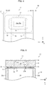
- FIG. 3 is a plan view of a transmission line 1A in accordance with Variation 1.
- (b) of Fig. 3 is a cross-sectional view of the transmission line 1A in accordance with Variation 1, the cross-sectional view being taken along the A-A' line shown in (a) of Fig. 3 .
- the transmission line 1A in accordance with Variation 1 is obtained by adding a bonding layer 32 to the transmission line 1 shown in Figs. 1 and 2 .
- the bonding layer 32 is provided between a conductor layer 13 of a PWW 11 and a short wall 23 of a waveguide tube 21 so as to bond the PWW 11 and the waveguide tube 21. Therefore, according to the transmission line 1A in accordance with Variation 1, the PWW 11 and the waveguide tube 21 are bonded by not only the bonding layer 31 but also the bonding layer 32.
- the bonding layer 31 corresponds to a "bonding layer” recited in the claims
- the bonding layer 32 corresponds to "another bonding layer” recited in the claims.
- the bonding layer 32 is made of a non-electrically conductive adhesive which has, after being cured, an elastic modulus smaller than that of the brittle material (in the present embodiment, quartz glass) of which the PWW 11 is made.
- the non-electrically conductive adhesive, of which the bonding layer 32 is made include acrylic resins, silicone resins, and epoxy resins.
- the bonding layer 32 is obtained by applying epoxy resin (thermal expansion coefficient: 30 ⁇ 10 -6 /K to 50 ⁇ 10 -6 /K, elastic modulus after curing: 2 GPa to 5 GPa) to a surface of the conductor layer 13 of the PWW 11 so as to surround the bonding layer 31, and then curing the epoxy resin.
- the non-electrically conductive adhesive can be applied by, for example, a method in which, after the waveguide tube 21 and the PWW 11 are bonded by the bonding layer 31 (i.e., after the electrically conductive adhesive for the bonding layer 31 is cured), a gap between the PWW 11 and the waveguide tube 21 is filled with the non-electrically conductive adhesive by use of a capillary flow technology.
- the non-electrically conductive adhesive thus applied is less likely to enter (i) a gap between the PWW 11 and the electrically conductive adhesive or (ii) a gap between the waveguide tube 21 and the electrically conductive adhesive. The conduction between the PWW 11 and the waveguide tube 21 is therefore less likely to be disturbed.
- the PWW 11 and the waveguide tube 21 are bonded by the bonding layer 31 alone.
- the PWW 11 and the waveguide tube 21 are bonded by not only the bonding layer 31 but also the bonding layer 32. This increases an area in which the PWW 11 and the waveguide tube 21 are bonded, and therefore enhances the strength by which the PWW 11 and the waveguide tube 21 are bonded.
- stress that is concentrated on the bonding layer 31 of the transmission line 1 is distributed not only to the bonding layer 31 but also to the bonding layer 32.
- the bonding layer 31 of the transmission line 1A in accordance with Variation 1 is therefore less likely to break due to the stress. Furthermore, the bonding layer 31 of the transmission line 1 is exposed to an external environment. In contrast, the bonding layer 31 of the transmission line 1A is not exposed to an external environment.
- the transmission line 1A in accordance with Variation 1 can therefore inhibit deterioration of the bonding layer 31, which deterioration may occur due to exposure to the external environment. Examples of such deterioration include (i) corrosion due to moisture absorption and (ii) conduction failure due to migration.
- Variation 1 was discussed with an example in which an outer periphery of the bonding layer 31 is entirely in contact with an inner periphery of the bonding layer 32. However, it is alternatively possible that the outer periphery of the bonding layer 31 is partially or entirely spaced from the inner periphery of the bonding layer 32.
- Fig. 4 is a plan view of a transmission line 1B in accordance with Variation 2.
- the transmission line 1B in accordance with Variation 2 is obtained by deforming the respective outer peripheries of the bonding layers 31 and 32 of the transmission line 1A shown in Fig. 3 .
- each of the bonding layers 31 and 32 has an angular outer periphery (specifically, a rectangular outer periphery).
- each of bonding layers 31 and 32 has an outer periphery whose corners are rounded (specifically, a rectangular outer periphery whose corners are rounded).
- the transmission line 1A in accordance with Variation 1 stress is likely to be concentrated on the four corners of each of the bonding layers 31 and 32.
- stress is less likely to be concentrated on the four corners of each of the bonding layers 31 and 32.
- the bonding layers 31 and 32 of the transmission line 1B in accordance with Variation 2 are therefore less likely to break due to concentration of stress.
- Fig. 5 is a cross-sectional view of a transmission line 1C in accordance with Variation 3.
- the transmission line 1C in accordance with Variation 3 is obtained by adding a solder layer 33 to the transmission line 1A shown in Fig. 3 .
- the solder layer 33 is provided on a short wall 23 of a waveguide tube 21 so as to surround an opening 23a.
- the solder layer 33 is made of AuSn90 solder (thermal expansion coefficient: 13.6 -6 / K, elastic modulus: 40 GPa).
- a bonding layer 31 is provided on a conductor layer 13 of a PWW 11, so as to surround an opening 13a.
- a bonding layer 32 is provided between the conductor layer 13 of the PWW 11 and the short wall 23 of the waveguide tube 21, so as to surround the bonding layer 31 and the solder layer 33.
- a space between the opening 13a of the PWW 11 and the opening 23a of the waveguide tube 21 is surrounded by the bonding layer 31 and the solder layer 33 each of which is electrically conductive. This makes it possible to inhibit electromagnetic wave leakage that may occur at a gap between the PWW 11 and the waveguide tube 21.
- an outer periphery of the bonding layer 31 can be partially or entirely spaced from an inner periphery of the bonding layer 32 and/or (ii) an outer periphery of the solder layer 33 can be partially or entirely spaced from an inner periphery of the bonding layer 32.
- a transmission line (1, 1A, 1B, or 1C) in accordance with the present embodiment includes: a first waveguide (11) which is made of a brittle material; a second waveguide (21); and a bonding layer (31) by which the first waveguide (11) and the second waveguide (21) are bonded and which is electrically conductive, at least part of the bonding layer (31) being made of an electrically conductive adhesive, the at least part of the bonding layer (31) being in contact with the first waveguide (11).
- the first waveguide and the second waveguide are bonded by the bonding layer. This eliminates the need for joining the first waveguide and the second waveguide together by screwing, soldering, or brazing. It is therefore possible to reduce the risk that the first waveguide made of a brittle material will be damaged due to the process of screwing, soldering, or brazing for joining the first waveguide and the second waveguide.
- the bonding layer is electrically conductive. This makes it possible to short-circuit the first waveguide and the second waveguide even though the first waveguide and the second waveguide are not joined with use of screws or the like.
- the transmission line (1, 1A, 1B, or 1C) in accordance with the present embodiment is preferably configured such that the electrically conductive adhesive has, after being cured, an elastic modulus smaller than that of the brittle material.
- the bonding layer has an elastic modulus smaller than that of the brittle material of which the first waveguide is made. This makes it possible to reduce stress that is applied to the first waveguide due to a difference in thermal expansion between the first waveguide and the second waveguide. It is therefore possible to reduce the risk that the first waveguide will be damaged due to stress applied to the first waveguide.
- the transmission line (1, 1A, 1B, or 1C) in accordance with the present embodiment is preferably configured such that a waveguide mode of the first waveguide (11) is coupled to that of the second waveguide (21) via respective openings (13a and 23a) of the first waveguide (11) and of the second waveguide (21); and the bonding layer (31) surrounds the respective openings (13a and 23a) of the first waveguide and of the second waveguide.
- the openings via which the waveguide mode of the first waveguide is coupled to that of the second waveguide are surrounded by the bonding layer made of an electrically conductive adhesive. It is therefore possible to inhibit electromagnetic wave leakage that may occur at a gap between the first waveguide and the second waveguide.
- the transmission line (1, 1A, 1B, or 1C) in accordance with the present embodiment is preferably configured such that the bonding layer (31) has an outer periphery whose corners are rounded.
- the transmission line (1A, 1B, or 1C) in accordance with the present embodiment is preferably configured to further include: another bonding layer (32) which is provided so as to surround the bonding layer (31) and which is made of a non-electrically conductive adhesive, the first waveguide (11) and the second waveguide (21) being bonded by not only the bonding layer (31) but also the another bonding layer (32).
- the first waveguide and the second waveguide are bonded by not only the bonding layer made of an electrically conductive adhesive but also the another bonding layer made of a non-electrically conductive adhesive.
- This increases an area in which the first waveguide and the second waveguide are bonded, and therefore enhances the strength by which the first waveguide and the second waveguide are bonded.
- the above configuration also makes it possible to distribute, to the another bonding layer, stress that is concentrated on the bonding layer. The bonding layer is therefore less likely to break due to the stress.
- the bonding layer is no longer exposed to an external environment. It is therefore possible to inhibit deterioration (e.g., corrosion or the like) of the bonding layer, which deterioration may occur due to exposure to the external environment.
- the transmission line (1A, 1B, or 1C) in accordance with the present embodiment is preferably configured such that the non-electrically conductive adhesive has, after being cured, an elastic modulus smaller than that of the brittle material.
- the another bonding layer has an elastic modulus smaller than that of the brittle material of which the first waveguide is made. This makes it possible to reduce stress that is applied to the first waveguide due to a difference in thermal expansion between the first waveguide and the second waveguide. It is therefore possible to reduce the risk that the first waveguide will be damaged due to stress applied to the first waveguide.
- the transmission line (1B or 1C) in accordance with the present embodiment is preferably configured such that the another bonding layer (32) has an outer periphery whose corners are rounded.
- the transmission line (1, 1A, 1B, or 1C) in accordance with the present embodiment is preferably configured such that the first waveguide (11) is a waveguide including (1) a dielectric substrate (12) which is made of the brittle material, (2) a first conductor layer (13) which is provided on a first main surface (12a) of the dielectric substrate (12), (3) a second conductor layer (14) which is provided on a second main surface (12b) of the dielectric substrate (12), and (4) at least one post wall (15 through 17) which is provided in the dielectric substrate (12); the first conductor layer (13) and the second conductor layer (14) each serve as a wide wall of the waveguide; and the at least one post wall (15 through 17) serves as a narrow wall of the waveguide.
- the above configuration makes it possible to produce the first waveguide that is thin and lightweight.
- the transmission line (1, 1A, 1B, or 1C) in accordance with the present embodiment is preferably configured such that the brittle material is quartz glass.
- the above configuration allows a reduction in dielectric loss of the first waveguide.
- the present invention is not limited to the foregoing embodiment, but can be altered by a skilled person in the art within the scope of the claims.
- the present invention also encompasses, in its technical scope, any embodiment derived by combining technical means disclosed in the foregoing embodiment and its variations.
Landscapes
- Waveguides (AREA)
- Waveguide Connection Structure (AREA)
Abstract
Description
- The present invention relates to a transmission line including a waveguide that is made of a brittle material.
- A dielectric waveguide, in which a conductor layer is provided on each of the front and back surfaces of a dielectric substrate, is advantageous in that it is suitable for transmission of millimeter waves and it can be thin in thickness. Examples of such a dielectric waveguide include the dielectric waveguide tube antenna disclosed in
Patent Literature 1. As a material for a substrate of a dielectric waveguide, quartz glass is promising because quartz glass has a small dielectric dissipation factor and therefore allows a reduction in dielectric loss (see Patent Literature 2). - Examples of a method for joining dielectric waveguides that constitute a transmission line include screwing, soldering, and brazing (see Patent Literature 3).
-
- [Patent Literature 1]
Japanese Patent No.4181085 - [Patent Literature 2]
Japanese Patent Application Publication Tokukai No.2014-265643 - [Patent Literature 3]
Japanese Patent Application Publication Tokukai No.2002-185203 - However, the following issues arise in a case where a conventional transmission line which includes two waveguides joined to each other is configured so that at least one of the two waveguides is made of a brittle material such as quartz glass. Note that the at least one of the two waveguides will be hereinafter referred to as "first waveguide".
- The first issue arises in a case where the two waveguides are joined by screwing. In order to join two waveguides by screwing, it is necessary to make screw holes in each of the two waveguides. However, in a case where screw holes are made in the first waveguide, mechanical strength of the first waveguide decreases. Furthermore, the first waveguide is highly likely to be (i) damaged while screw holes are being made and/or (ii) damaged, after screw holes have been made, due to a scratch made while the screw holes were being made.
- The second issue arises in a case where the two waveguides are joined by soldering or brazing. In a case where the two waveguides are joined by soldering, the respective temperatures of the two waveguides increase while solder is being melted, and the respective temperatures of the two waveguides decrease while solder is being cured. Stress is therefore applied to the first waveguide due to a difference in thermal expansion between the first waveguide and the second waveguide. Furthermore, stress is applied to the first waveguide also during solidification shrinkage of solder. These stresses are highly likely to damage the first waveguide. The same issue arises in a case where the two waveguides are joined by brazing.
- The present invention was attained in view of the above issues, and an object of the present invention is to provide a transmission line in which a waveguide made of a brittle material is unlikely to be damaged.
- A transmission line in accordance with an aspect of the present invention includes: a first waveguide which is made of a brittle material; a second waveguide; and a bonding layer by which the first waveguide and the second waveguide are bonded and which is electrically conductive, at least part of the bonding layer being made of an electrically conductive adhesive, the at least part of the bonding layer being in contact with the first waveguide.
- An aspect of the present invention makes it possible to provide a transmission line in which a waveguide made of a brittle material is unlikely to be damaged.
-
-
Fig. 1 is an exploded perspective view of a transmission line in accordance withEmbodiment 1 of the present invention. - (a) of
Fig. 2 is a plan view of the transmission line shown inFig. 1 . (b) ofFig. 2 is a cross-sectional view of the transmission line shown inFig. 1 . - (a) of
Fig. 3 is a plan view ofVariation 1 of the transmission line shown inFig. 1 . (b) ofFig. 3 is a cross-sectional view of the transmission line shown in (a) ofFig. 3 . -
Fig. 4 is a plan view of Variation 2 of the transmission line shown inFig. 1 . -
Fig. 5 is a cross-sectional view of Variation 3 of the transmission line shown inFig. 1 . - The following description will discuss, with reference to
Figs. 1 and2 , a transmission line in accordance with an embodiment of the present invention.Fig. 1 is an exploded perspective view of atransmission line 1 in accordance with the present embodiment. (a) ofFig. 2 is a plan view of thetransmission line 1 shown inFig. 1 . (b) ofFig. 2 is a cross-sectional view of thetransmission line 1 shown inFig. 1 , the cross-sectional view being taken along the A-A' line shown in (a) ofFig. 2 . Note that the coordinate system shown inFigs. 1 and2 is set so that (i) the y-axis positive direction matches a direction in which an electromagnetic wave is to be guided through apost-wall waveguide 11 and (ii) the z-axis positive direction matches a direction in which the electromagnetic wave is then guided through awaveguide tube 21. The x-axis positive direction of the coordinate system is set so as to constitute, together with the y-axis positive direction and the z-axis positive direction defined as described above, a right-handed coordinate system. Hereinafter, a post-wall waveguide will be abbreviated as "PWW". - The
transmission line 1 is a transmission line that is suitable for transmission of millimeter waves. Thetransmission line 1 includes the post-wall waveguide 11 (corresponding to a "first waveguide" recited in the claims), the waveguide tube 21 (corresponding to a "second waveguide" recited in the claims), and abonding layer 31 by which thepost-wall waveguide 11 and thewaveguide tube 21 are bonded. A post-wall waveguide, whose narrow walls are each constituted by a post wall, is advantageous in that a lighter weight can be achieved in comparison with a dielectric waveguide, whose narrow walls are each constituted by a conductor plate. - The
PWW 11 includes (i) a substrate 12 (corresponding to a "dielectric substrate" recited in the claims), (ii) afirst conductor layer 13 which is provided on a firstmain surface 12a of thesubstrate 12, and (iii) asecond conductor layer 14 which is provided on a secondmain surface 12b of thesubstrate 12. Each of thefirst conductor layer 13 and thesecond conductor layer 14 serves as a wide wall of thePWW 11. - The
substrate 12 is made of a dielectric brittle material. Examples of such a brittle material, of which thesubstrate 12 is made, include glass (e.g., quartz glass) and ceramic. According to the present embodiment, the brittle material, of which thesubstrate 12 is made, is quartz glass (thermal expansion coefficient: 0.5 × 10⁻⁶ /K, elastic modulus: 73 GPa). - The
substrate 12 includespost walls post wall 15 is constituted by a plurality ofconductor posts 15i which are arranged in a fence-like manner. Note here that "i" is a natural number that satisfies 1 ≤ i ≤ L ("L" is a natural number that represents the number of theconductor posts 15i). Each of the plurality ofconductor posts 15i is obtained by (i) making a via that passes through thesubstrate 12 from the firstmain surface 12a to the secondmain surface 12b, and then (ii) filling the via with an electric conductor such as metal or depositing such an electric conductor on the inner wall of the via. In a case where the plurality ofconductor posts 15i are arranged at intervals each sufficiently smaller than a wavelength of an electromagnetic wave to be guided through thePWW 11, thepost wall 15 serves as a reflection wall. Similarly to thepost wall 15, thepost wall 16 is constituted by a plurality ofconductor posts 16j, thepost wall 17 is constituted by a plurality ofconductor posts 17k, and each of thepost walls conductor posts 16j), and "k" is a natural number that satisfies 1 ≤ k ≤ N ("N" is a natural number that represents the number of theconductor posts 17k). - In
Fig. 1 , the narrow walls achieved by therespective post walls Fig. 1 , some parts of thepost walls - The
substrate 12 has a rectangular-parallelepiped region that is surrounded by the conductor layers 13 and 14 and thepost walls 15 through 17. This rectangular-parallelepiped region serves as apropagation region 18 through which an electromagnetic wave propagates. In thepropagation region 18, an electromagnetic wave propagates along the y-axis of the coordinate system shown inFig. 1 . - The
conductor layer 13 has anopening 13a which is provided in the vicinity of one end portion of thepropagation region 18 so as to serve as the entrance and the exit of thepropagation region 18. Theopening 13a has a rectangular shape, and is oriented such that long sides of theopening 13a are orthogonal to the lengthwise direction of the propagation region 18 (i.e., orthogonal to the y-axis direction shown inFig. 1 ). - The
waveguide tube 21 is a quadrangular waveguide tube including atube wall 22 which is constituted by (i) a pair ofwide walls narrow walls waveguide tube 21 is closed with ashort wall 23. Theshort wall 23 has anopening 23a which is identical in shape to theopening 13a of thePWW 11. Thewaveguide tube 21 can either be hollow or be filled with a dielectric that is different from air. - The waveguide tube 21 (i.e., the
tube wall 22 and the short wall 23) is made of a conductor material. Examples of the conductor material, of which thewaveguide tube 21 is made, include copper and brass. According to the present embodiment, the conductor material, of which thewaveguide tube 21 is made, is copper (thermal expansion coefficient: 16.8 × 10⁻⁶ /K, elastic modulus: 129 GPa). - The four sides of the
tube wall 22 form a rectangular-parallelepiped region therein. The rectangular-parallelepiped region serves as apropagation region 24 through which an electromagnetic wave propagates. In thepropagation region 24, an electromagnetic wave propagates along the z-axis of the coordinate system shown inFig. 1 . - The
waveguide tube 21 is arranged such that (i) theshort wall 23 faces theconductor layer 13 of thePWW 11 and (ii) theopening 23a of theshort wall 23 overlaps theopening 13a of theconductor layer 13. Thepropagation region 24 of thewaveguide tube 21 communicates with thepropagation region 18 of thePWW 11 via theopening 23a and theopening 13a. That is, a waveguide mode of thewaveguide tube 21 is coupled to that of thePWW 11 via theopening 23a and theopening 13a. - The
bonding layer 31 is provided between theconductor layer 13 of thePWW 11 and theshort wall 23 of thewaveguide tube 21 so as to bond thePWW 11 and thewaveguide tube 21. Thebonding layer 31 is made of an electrically conductive adhesive which has, after being cured, an elastic modulus smaller than that of the brittle material (in the present embodiment, quartz glass) of which thePWW 11 is made. Examples of the electrically conductive adhesive include: a silver paste obtained by adding a silver filler to a resin; and a copper paste obtained by adding a copper filler to a resin. - According to the present embodiment, the
bonding layer 31 is obtained by applying a silver paste (thermal expansion coefficient: 30 × 10-6 /K to 50 × 10-6 /K, elastic modulus after curing: 5 GPa) to a surface of theconductor layer 13 of thePWW 11 so as to surround theopening 13a, and then curing the silver paste. The silver paste can be applied by use of any conventional technique, examples of which include (i) a method in which a dispenser is used, (ii) a transfer printing method, and (iii) a printing method. - According to the
transmission line 1 in accordance with the present embodiment, it is unnecessary to join thePWW 11 and thewaveguide tube 21 with use of a screw(s) because thePWW 11 and thewaveguide tube 21 are bonded by thebonding layer 31. This eliminates the need for making screw holes in thePWW 11. ThePWW 11 is therefore less likely to be (i) damaged while screw holes are being made and/or (ii) damaged, after screw holes have been made, due to a scratch made while the screw holes were being made. - Since the
bonding layer 31 is electrically conductive, it is possible to short-circuit thePWW 11 and thewaveguide tube 21 even though thePWW 11 and thewaveguide tube 21 are not joined with use of screws. Furthermore, since thebonding layer 31 has an elastic modulus smaller than that of the brittle material of which thePWW 11 is made, it is possible to reduce stress that is applied to thePWW 11 due to a difference in thermal expansion between thePWW 11 and thewaveguide tube 21. Furthermore, since thebonding layer 31 having an electrical conductivity surrounds theopening 13a of thePWW 11 and theopening 23a of thewaveguide tube 21, it is possible to inhibit electromagnetic wave leakage that may occur at a gap between thePWW 11 and thewaveguide tube 21. - The following description will discuss
Variation 1 of thetransmission line 1 with reference toFig. 3 . (a) ofFig. 3 is a plan view of a transmission line 1A in accordance withVariation 1. (b) ofFig. 3 is a cross-sectional view of the transmission line 1A in accordance withVariation 1, the cross-sectional view being taken along the A-A' line shown in (a) ofFig. 3 . - The transmission line 1A in accordance with
Variation 1 is obtained by adding abonding layer 32 to thetransmission line 1 shown inFigs. 1 and2 . Similarly to abonding layer 31, thebonding layer 32 is provided between aconductor layer 13 of aPWW 11 and ashort wall 23 of awaveguide tube 21 so as to bond thePWW 11 and thewaveguide tube 21. Therefore, according to the transmission line 1A in accordance withVariation 1, thePWW 11 and thewaveguide tube 21 are bonded by not only thebonding layer 31 but also thebonding layer 32. Note here that thebonding layer 31 corresponds to a "bonding layer" recited in the claims, and thebonding layer 32 corresponds to "another bonding layer" recited in the claims. - The
bonding layer 32 is made of a non-electrically conductive adhesive which has, after being cured, an elastic modulus smaller than that of the brittle material (in the present embodiment, quartz glass) of which thePWW 11 is made. Examples of the non-electrically conductive adhesive, of which thebonding layer 32 is made, include acrylic resins, silicone resins, and epoxy resins. According to the present embodiment, thebonding layer 32 is obtained by applying epoxy resin (thermal expansion coefficient: 30 × 10-6 /K to 50 × 10-6 /K, elastic modulus after curing: 2 GPa to 5 GPa) to a surface of theconductor layer 13 of thePWW 11 so as to surround thebonding layer 31, and then curing the epoxy resin. - The non-electrically conductive adhesive can be applied by, for example, a method in which, after the
waveguide tube 21 and thePWW 11 are bonded by the bonding layer 31 (i.e., after the electrically conductive adhesive for thebonding layer 31 is cured), a gap between thePWW 11 and thewaveguide tube 21 is filled with the non-electrically conductive adhesive by use of a capillary flow technology. The non-electrically conductive adhesive thus applied is less likely to enter (i) a gap between thePWW 11 and the electrically conductive adhesive or (ii) a gap between thewaveguide tube 21 and the electrically conductive adhesive. The conduction between thePWW 11 and thewaveguide tube 21 is therefore less likely to be disturbed. - According to the
transmission line 1, thePWW 11 and thewaveguide tube 21 are bonded by thebonding layer 31 alone. In contrast, according to the transmission line 1A in accordance withVariation 1, thePWW 11 and thewaveguide tube 21 are bonded by not only thebonding layer 31 but also thebonding layer 32. This increases an area in which thePWW 11 and thewaveguide tube 21 are bonded, and therefore enhances the strength by which thePWW 11 and thewaveguide tube 21 are bonded. Furthermore, according to the transmission line 1A in accordance withVariation 1, stress that is concentrated on thebonding layer 31 of thetransmission line 1 is distributed not only to thebonding layer 31 but also to thebonding layer 32. Thebonding layer 31 of the transmission line 1A in accordance withVariation 1 is therefore less likely to break due to the stress. Furthermore, thebonding layer 31 of thetransmission line 1 is exposed to an external environment. In contrast, thebonding layer 31 of the transmission line 1A is not exposed to an external environment. The transmission line 1A in accordance withVariation 1 can therefore inhibit deterioration of thebonding layer 31, which deterioration may occur due to exposure to the external environment. Examples of such deterioration include (i) corrosion due to moisture absorption and (ii) conduction failure due to migration. -
Variation 1 was discussed with an example in which an outer periphery of thebonding layer 31 is entirely in contact with an inner periphery of thebonding layer 32. However, it is alternatively possible that the outer periphery of thebonding layer 31 is partially or entirely spaced from the inner periphery of thebonding layer 32. - The following description will discuss Variation 2 of the
transmission line 1 with reference toFig. 4. Fig. 4 is a plan view of atransmission line 1B in accordance with Variation 2. - The
transmission line 1B in accordance with Variation 2 is obtained by deforming the respective outer peripheries of the bonding layers 31 and 32 of the transmission line 1A shown inFig. 3 . According to the transmission line 1A, each of the bonding layers 31 and 32 has an angular outer periphery (specifically, a rectangular outer periphery). In contrast, according to thetransmission line 1B, each of bonding layers 31 and 32 has an outer periphery whose corners are rounded (specifically, a rectangular outer periphery whose corners are rounded). - According to the transmission line 1A in accordance with
Variation 1, stress is likely to be concentrated on the four corners of each of the bonding layers 31 and 32. In contrast, according to thetransmission line 1B in accordance with Variation 2, stress is less likely to be concentrated on the four corners of each of the bonding layers 31 and 32. The bonding layers 31 and 32 of thetransmission line 1B in accordance with Variation 2 are therefore less likely to break due to concentration of stress. - The following description will discuss Variation 3 of the
transmission line 1 with reference toFig. 5. Fig. 5 is a cross-sectional view of atransmission line 1C in accordance with Variation 3. - The
transmission line 1C in accordance with Variation 3 is obtained by adding asolder layer 33 to the transmission line 1A shown inFig. 3 . Thesolder layer 33 is provided on ashort wall 23 of awaveguide tube 21 so as to surround anopening 23a. According to Variation 3, thesolder layer 33 is made of AuSn90 solder (thermal expansion coefficient: 13.6-6 / K, elastic modulus: 40 GPa). Abonding layer 31 is provided on aconductor layer 13 of aPWW 11, so as to surround anopening 13a. Abonding layer 32 is provided between theconductor layer 13 of thePWW 11 and theshort wall 23 of thewaveguide tube 21, so as to surround thebonding layer 31 and thesolder layer 33. - According to the
transmission line 1C in accordance with Variation 3, a space between theopening 13a of thePWW 11 and theopening 23a of thewaveguide tube 21 is surrounded by thebonding layer 31 and thesolder layer 33 each of which is electrically conductive. This makes it possible to inhibit electromagnetic wave leakage that may occur at a gap between thePWW 11 and thewaveguide tube 21. - According to Variation 3, (i) an outer periphery of the
bonding layer 31 can be partially or entirely spaced from an inner periphery of thebonding layer 32 and/or (ii) an outer periphery of thesolder layer 33 can be partially or entirely spaced from an inner periphery of thebonding layer 32. - Aspects of the present invention can also be expressed as follows:
A transmission line (1, 1A, 1B, or 1C) in accordance with the present embodiment includes: a first waveguide (11) which is made of a brittle material; a second waveguide (21); and a bonding layer (31) by which the first waveguide (11) and the second waveguide (21) are bonded and which is electrically conductive, at least part of the bonding layer (31) being made of an electrically conductive adhesive, the at least part of the bonding layer (31) being in contact with the first waveguide (11). - According to the above configuration, the first waveguide and the second waveguide are bonded by the bonding layer. This eliminates the need for joining the first waveguide and the second waveguide together by screwing, soldering, or brazing. It is therefore possible to reduce the risk that the first waveguide made of a brittle material will be damaged due to the process of screwing, soldering, or brazing for joining the first waveguide and the second waveguide.
- According to the above configuration, the bonding layer is electrically conductive. This makes it possible to short-circuit the first waveguide and the second waveguide even though the first waveguide and the second waveguide are not joined with use of screws or the like.
- The transmission line (1, 1A, 1B, or 1C) in accordance with the present embodiment is preferably configured such that the electrically conductive adhesive has, after being cured, an elastic modulus smaller than that of the brittle material.
- According to the above configuration, the bonding layer has an elastic modulus smaller than that of the brittle material of which the first waveguide is made. This makes it possible to reduce stress that is applied to the first waveguide due to a difference in thermal expansion between the first waveguide and the second waveguide. It is therefore possible to reduce the risk that the first waveguide will be damaged due to stress applied to the first waveguide.
- The transmission line (1, 1A, 1B, or 1C) in accordance with the present embodiment is preferably configured such that a waveguide mode of the first waveguide (11) is coupled to that of the second waveguide (21) via respective openings (13a and 23a) of the first waveguide (11) and of the second waveguide (21); and the bonding layer (31) surrounds the respective openings (13a and 23a) of the first waveguide and of the second waveguide.
- According to the above configuration, the openings via which the waveguide mode of the first waveguide is coupled to that of the second waveguide are surrounded by the bonding layer made of an electrically conductive adhesive. It is therefore possible to inhibit electromagnetic wave leakage that may occur at a gap between the first waveguide and the second waveguide.
- The transmission line (1, 1A, 1B, or 1C) in accordance with the present embodiment is preferably configured such that the bonding layer (31) has an outer periphery whose corners are rounded.
- The above configuration makes it possible to reduce the risk that the bonding layer will break due to concentration of stress.
- The transmission line (1A, 1B, or 1C) in accordance with the present embodiment is preferably configured to further include: another bonding layer (32) which is provided so as to surround the bonding layer (31) and which is made of a non-electrically conductive adhesive, the first waveguide (11) and the second waveguide (21) being bonded by not only the bonding layer (31) but also the another bonding layer (32).
- According to the above configuration, the first waveguide and the second waveguide are bonded by not only the bonding layer made of an electrically conductive adhesive but also the another bonding layer made of a non-electrically conductive adhesive. This increases an area in which the first waveguide and the second waveguide are bonded, and therefore enhances the strength by which the first waveguide and the second waveguide are bonded. The above configuration also makes it possible to distribute, to the another bonding layer, stress that is concentrated on the bonding layer. The bonding layer is therefore less likely to break due to the stress. Furthermore, since the bonding layer is surrounded by the another bonding layer, the bonding layer is no longer exposed to an external environment. It is therefore possible to inhibit deterioration (e.g., corrosion or the like) of the bonding layer, which deterioration may occur due to exposure to the external environment.
- The transmission line (1A, 1B, or 1C) in accordance with the present embodiment is preferably configured such that the non-electrically conductive adhesive has, after being cured, an elastic modulus smaller than that of the brittle material.
- According to the above configuration, the another bonding layer has an elastic modulus smaller than that of the brittle material of which the first waveguide is made. This makes it possible to reduce stress that is applied to the first waveguide due to a difference in thermal expansion between the first waveguide and the second waveguide. It is therefore possible to reduce the risk that the first waveguide will be damaged due to stress applied to the first waveguide.
- The transmission line (1B or 1C) in accordance with the present embodiment is preferably configured such that the another bonding layer (32) has an outer periphery whose corners are rounded.
- The above configuration makes it possible to reduce the risk that the another bonding layer will break due to concentration of stress.
- The transmission line (1, 1A, 1B, or 1C) in accordance with the present embodiment is preferably configured such that the first waveguide (11) is a waveguide including (1) a dielectric substrate (12) which is made of the brittle material, (2) a first conductor layer (13) which is provided on a first main surface (12a) of the dielectric substrate (12), (3) a second conductor layer (14) which is provided on a second main surface (12b) of the dielectric substrate (12), and (4) at least one post wall (15 through 17) which is provided in the dielectric substrate (12); the first conductor layer (13) and the second conductor layer (14) each serve as a wide wall of the waveguide; and the at least one post wall (15 through 17) serves as a narrow wall of the waveguide.
- The above configuration makes it possible to produce the first waveguide that is thin and lightweight.
- The transmission line (1, 1A, 1B, or 1C) in accordance with the present embodiment is preferably configured such that the brittle material is quartz glass.
- The above configuration allows a reduction in dielectric loss of the first waveguide.
- The present invention is not limited to the foregoing embodiment, but can be altered by a skilled person in the art within the scope of the claims. The present invention also encompasses, in its technical scope, any embodiment derived by combining technical means disclosed in the foregoing embodiment and its variations.
-
- 1, 1A, 1B, 1C: Transmission line
- 11: Post-wall waveguide (first waveguide)
- 12: Substrate
- 12a: First main surface
- 12b: Second main surface
- 13: Conductor layer (first conductor layer)
- 13a: Opening
- 14: Conductor layer (second conductor layer)
- 15, 16, 17: Post wall
- 18: Propagation region
- 21: Waveguide tube (second waveguide)
- 22: Tube wall
- 23: Short wall
- 23a: Opening
- 24: Propagation region
- 31: Bonding layer (electrically conductive adhesive)
- 32: Bonding layer (non-electrically conductive adhesive)
- 33: Solder layer
Claims (9)
- A transmission line, comprising:a first waveguide which is made of a brittle material;a second waveguide; anda bonding layer by which the first waveguide and the second waveguide are bonded and which is electrically conductive,at least part of the bonding layer being made of an electrically conductive adhesive, the at least part of the bonding layer being in contact with the first waveguide.
- The transmission line as set forth in claim 1, wherein the electrically conductive adhesive has, after being cured, an elastic modulus smaller than that of the brittle material.
- The transmission line as set forth in claim 1 or 2, wherein:a waveguide mode of the first waveguide is coupled to that of the second waveguide via respective openings of the first waveguide and of the second waveguide; andthe bonding layer surrounds the respective openings of the first waveguide and of the second waveguide.
- The transmission line as set forth in any one of claims 1 through 3, wherein the bonding layer has an outer periphery whose corners are rounded.
- The transmission line as set forth in any one of claims 1 through 4, further comprising:another bonding layer which is provided so as to surround the bonding layer and which is made of a non-electrically conductive adhesive,the first waveguide and the second waveguide being bonded by not only the bonding layer but also the another bonding layer.
- The transmission line as set forth in claim 5, wherein the non-electrically conductive adhesive has, after being cured, an elastic modulus smaller than that of the brittle material.
- The transmission line as set forth in claim 5 or 6, wherein the another bonding layer has an outer periphery whose corners are rounded.
- The transmission line as set forth in any one of claims 1 through 7, wherein:the first waveguide is a waveguide including (1) a dielectric substrate which is made of the brittle material, (2) a first conductor layer which is provided on a first main surface of the dielectric substrate, (3) a second conductor layer which is provided on a second main surface of the dielectric substrate, and (4) at least one post wall which is provided in the dielectric substrate;the first conductor layer and the second conductor layer each serve as a wide wall of the waveguide; andthe at least one post wall serves as a narrow wall of the waveguide.
- The transmission line as set forth in any one of claims 1 through 8, wherein the brittle material is quartz glass.
Applications Claiming Priority (2)
| Application Number | Priority Date | Filing Date | Title |
|---|---|---|---|
| JP2017133964A JP6861588B2 (en) | 2017-07-07 | 2017-07-07 | Transmission line |
| PCT/JP2018/015237 WO2019008859A1 (en) | 2017-07-07 | 2018-04-11 | Transmission line |
Publications (3)
| Publication Number | Publication Date |
|---|---|
| EP3651265A1 true EP3651265A1 (en) | 2020-05-13 |
| EP3651265A4 EP3651265A4 (en) | 2021-03-03 |
| EP3651265B1 EP3651265B1 (en) | 2021-09-29 |
Family
ID=64950730
Family Applications (1)
| Application Number | Title | Priority Date | Filing Date |
|---|---|---|---|
| EP18828521.7A Not-in-force EP3651265B1 (en) | 2017-07-07 | 2018-04-11 | Transmission line |
Country Status (4)
| Country | Link |
|---|---|
| US (1) | US11158922B2 (en) |
| EP (1) | EP3651265B1 (en) |
| JP (1) | JP6861588B2 (en) |
| WO (1) | WO2019008859A1 (en) |
Families Citing this family (2)
| Publication number | Priority date | Publication date | Assignee | Title |
|---|---|---|---|---|
| JP6902567B2 (en) * | 2019-03-13 | 2021-07-14 | 株式会社フジクラ | Conversion structure |
| DE102021117640A1 (en) * | 2021-07-08 | 2023-01-12 | Tesat-Spacecom Gmbh & Co. Kg | Waveguide arrangement with two ridge waveguides and connection interface |
Family Cites Families (13)
| Publication number | Priority date | Publication date | Assignee | Title |
|---|---|---|---|---|
| JP3522120B2 (en) * | 1998-08-31 | 2004-04-26 | 京セラ株式会社 | Connection structure of dielectric waveguide line |
| US6515562B1 (en) | 1998-04-23 | 2003-02-04 | Kyocera Corporation | Connection structure for overlapping dielectric waveguide lines |
| JP3628238B2 (en) * | 2000-06-28 | 2005-03-09 | 京セラ株式会社 | Wiring board and its connection structure with waveguide |
| US6870438B1 (en) | 1999-11-10 | 2005-03-22 | Kyocera Corporation | Multi-layered wiring board for slot coupling a transmission line to a waveguide |
| DE60024684T2 (en) * | 2000-10-06 | 2006-06-22 | Nokia Corp. | SELF-ORIENTAL TRANSITION BETWEEN A TRANSMISSION LINE AND A MODULE |
| JP3617633B2 (en) | 2000-10-06 | 2005-02-09 | 三菱電機株式会社 | Waveguide connection |
| US7064633B2 (en) * | 2002-07-13 | 2006-06-20 | The Chinese University Of Hong Kong | Waveguide to laminated waveguide transition and methodology |
| JP4181085B2 (en) | 2004-05-31 | 2008-11-12 | 東光株式会社 | Dielectric waveguide antenna |
| JP2010081486A (en) | 2008-09-29 | 2010-04-08 | Kyocera Corp | Waveguide connecting structure, and front end using the same |
| KR101729179B1 (en) * | 2012-11-26 | 2017-05-11 | 한국전자통신연구원 | structure for connecting electrical trace lines of printed circuit boards and optical transmission/reception module having the same |
| US9123979B1 (en) | 2013-03-28 | 2015-09-01 | Google Inc. | Printed waveguide transmission line having layers with through-holes having alternating greater/lesser widths in adjacent layers |
| JP5727069B1 (en) * | 2014-04-23 | 2015-06-03 | 株式会社フジクラ | Waveguide type slot array antenna and slot array antenna module |
| JP2016127378A (en) | 2014-12-26 | 2016-07-11 | 株式会社フジクラ | High frequency substrate fixing jig and high frequency substrate characteristic measuring method |
-
2017
- 2017-07-07 JP JP2017133964A patent/JP6861588B2/en not_active Expired - Fee Related
-
2018
- 2018-04-11 US US16/619,509 patent/US11158922B2/en not_active Expired - Fee Related
- 2018-04-11 EP EP18828521.7A patent/EP3651265B1/en not_active Not-in-force
- 2018-04-11 WO PCT/JP2018/015237 patent/WO2019008859A1/en not_active Ceased
Also Published As
| Publication number | Publication date |
|---|---|
| US20200099118A1 (en) | 2020-03-26 |
| EP3651265A4 (en) | 2021-03-03 |
| JP6861588B2 (en) | 2021-04-21 |
| JP2019016955A (en) | 2019-01-31 |
| US11158922B2 (en) | 2021-10-26 |
| EP3651265B1 (en) | 2021-09-29 |
| WO2019008859A1 (en) | 2019-01-10 |
Similar Documents
| Publication | Publication Date | Title |
|---|---|---|
| CN1596485B (en) | Method of forming a waveguide in a printed circuit board | |
| CN101421648B (en) | Opto-electric hybrid film and electronic device housing the same | |
| WO2013189513A1 (en) | Directional coupler waveguide structure and method | |
| JP2013126099A5 (en) | ||
| JP2012018289A (en) | Optical module | |
| CN112993058B (en) | An optoelectronic microsystem packaging structure based on hybrid integration technology | |
| JP6182422B2 (en) | Connection structure with waveguide | |
| CN104508810A (en) | Wiring substrate | |
| EP3651265B1 (en) | Transmission line | |
| KR20170086757A (en) | Printed-circuit board having electromagnetic-tunnel-embedded arhchitecture and manufacturing method thereof | |
| CN109417214B (en) | Waveguide-Planar Waveguide Converter | |
| JP2019008269A (en) | Optical waveguide and optical circuit board | |
| WO2004059784A1 (en) | Dielectric filter | |
| WO2018164159A1 (en) | Module | |
| US20100321136A1 (en) | Waveguide transition arragement | |
| US11394100B2 (en) | High-frequency connection structure for connecting a coaxial line to a planar line using adhesion layers | |
| US11631506B2 (en) | High-frequency line connection structure | |
| JP4164947B2 (en) | Optical / electrical wiring board, manufacturing method, and mounting board | |
| JPS6179290A (en) | Optical/electronic printed circuit board | |
| JP2007123950A (en) | Coaxial line-flat substrate conversion structure and high-frequency signal converter | |
| JP2008159862A (en) | Package structure of high frequency electronic components | |
| CN103633403A (en) | Transmission line and method for manufacturing same | |
| US20250253510A1 (en) | Mode conversion device | |
| JP3399771B2 (en) | Microwave circuit | |
| JPH09162631A (en) | antenna |
Legal Events
| Date | Code | Title | Description |
|---|---|---|---|
| STAA | Information on the status of an ep patent application or granted ep patent |
Free format text: STATUS: THE INTERNATIONAL PUBLICATION HAS BEEN MADE |
|
| PUAI | Public reference made under article 153(3) epc to a published international application that has entered the european phase |
Free format text: ORIGINAL CODE: 0009012 |
|
| STAA | Information on the status of an ep patent application or granted ep patent |
Free format text: STATUS: REQUEST FOR EXAMINATION WAS MADE |
|
| 17P | Request for examination filed |
Effective date: 20191226 |
|
| AK | Designated contracting states |
Kind code of ref document: A1 Designated state(s): AL AT BE BG CH CY CZ DE DK EE ES FI FR GB GR HR HU IE IS IT LI LT LU LV MC MK MT NL NO PL PT RO RS SE SI SK SM TR |
|
| AX | Request for extension of the european patent |
Extension state: BA ME |
|
| DAV | Request for validation of the european patent (deleted) | ||
| DAX | Request for extension of the european patent (deleted) | ||
| A4 | Supplementary search report drawn up and despatched |
Effective date: 20210203 |
|
| RIC1 | Information provided on ipc code assigned before grant |
Ipc: H01P 3/12 20060101ALN20210128BHEP Ipc: H01P 5/08 20060101AFI20210128BHEP |
|
| REG | Reference to a national code |
Ref country code: DE Ref legal event code: R079 Ref document number: 602018024415 Country of ref document: DE Free format text: PREVIOUS MAIN CLASS: H01P0005080000 Ipc: H01P0001020000 |
|
| GRAP | Despatch of communication of intention to grant a patent |
Free format text: ORIGINAL CODE: EPIDOSNIGR1 |
|
| STAA | Information on the status of an ep patent application or granted ep patent |
Free format text: STATUS: GRANT OF PATENT IS INTENDED |
|
| RIC1 | Information provided on ipc code assigned before grant |
Ipc: H01P 5/02 20060101ALI20210601BHEP Ipc: H01P 3/12 20060101ALI20210601BHEP Ipc: H01P 1/02 20060101AFI20210601BHEP |
|
| INTG | Intention to grant announced |
Effective date: 20210624 |
|
| RIN1 | Information on inventor provided before grant (corrected) |
Inventor name: MATSUMARU, KOHEI |
|
| GRAS | Grant fee paid |
Free format text: ORIGINAL CODE: EPIDOSNIGR3 |
|
| GRAA | (expected) grant |
Free format text: ORIGINAL CODE: 0009210 |
|
| STAA | Information on the status of an ep patent application or granted ep patent |
Free format text: STATUS: THE PATENT HAS BEEN GRANTED |
|
| AK | Designated contracting states |
Kind code of ref document: B1 Designated state(s): AL AT BE BG CH CY CZ DE DK EE ES FI FR GB GR HR HU IE IS IT LI LT LU LV MC MK MT NL NO PL PT RO RS SE SI SK SM TR |
|
| REG | Reference to a national code |
Ref country code: GB Ref legal event code: FG4D |
|
| REG | Reference to a national code |
Ref country code: CH Ref legal event code: EP Ref country code: AT Ref legal event code: REF Ref document number: 1435007 Country of ref document: AT Kind code of ref document: T Effective date: 20211015 |
|
| REG | Reference to a national code |
Ref country code: DE Ref legal event code: R096 Ref document number: 602018024415 Country of ref document: DE |
|
| REG | Reference to a national code |
Ref country code: IE Ref legal event code: FG4D |
|
| REG | Reference to a national code |
Ref country code: LT Ref legal event code: MG9D |
|
| PG25 | Lapsed in a contracting state [announced via postgrant information from national office to epo] |
Ref country code: BG Free format text: LAPSE BECAUSE OF FAILURE TO SUBMIT A TRANSLATION OF THE DESCRIPTION OR TO PAY THE FEE WITHIN THE PRESCRIBED TIME-LIMIT Effective date: 20211229 Ref country code: LT Free format text: LAPSE BECAUSE OF FAILURE TO SUBMIT A TRANSLATION OF THE DESCRIPTION OR TO PAY THE FEE WITHIN THE PRESCRIBED TIME-LIMIT Effective date: 20210929 Ref country code: NO Free format text: LAPSE BECAUSE OF FAILURE TO SUBMIT A TRANSLATION OF THE DESCRIPTION OR TO PAY THE FEE WITHIN THE PRESCRIBED TIME-LIMIT Effective date: 20211229 Ref country code: HR Free format text: LAPSE BECAUSE OF FAILURE TO SUBMIT A TRANSLATION OF THE DESCRIPTION OR TO PAY THE FEE WITHIN THE PRESCRIBED TIME-LIMIT Effective date: 20210929 Ref country code: FI Free format text: LAPSE BECAUSE OF FAILURE TO SUBMIT A TRANSLATION OF THE DESCRIPTION OR TO PAY THE FEE WITHIN THE PRESCRIBED TIME-LIMIT Effective date: 20210929 Ref country code: RS Free format text: LAPSE BECAUSE OF FAILURE TO SUBMIT A TRANSLATION OF THE DESCRIPTION OR TO PAY THE FEE WITHIN THE PRESCRIBED TIME-LIMIT Effective date: 20210929 Ref country code: SE Free format text: LAPSE BECAUSE OF FAILURE TO SUBMIT A TRANSLATION OF THE DESCRIPTION OR TO PAY THE FEE WITHIN THE PRESCRIBED TIME-LIMIT Effective date: 20210929 |
|
| REG | Reference to a national code |
Ref country code: NL Ref legal event code: MP Effective date: 20210929 |
|
| REG | Reference to a national code |
Ref country code: AT Ref legal event code: MK05 Ref document number: 1435007 Country of ref document: AT Kind code of ref document: T Effective date: 20210929 |
|
| PG25 | Lapsed in a contracting state [announced via postgrant information from national office to epo] |
Ref country code: LV Free format text: LAPSE BECAUSE OF FAILURE TO SUBMIT A TRANSLATION OF THE DESCRIPTION OR TO PAY THE FEE WITHIN THE PRESCRIBED TIME-LIMIT Effective date: 20210929 Ref country code: GR Free format text: LAPSE BECAUSE OF FAILURE TO SUBMIT A TRANSLATION OF THE DESCRIPTION OR TO PAY THE FEE WITHIN THE PRESCRIBED TIME-LIMIT Effective date: 20211230 |
|
| PG25 | Lapsed in a contracting state [announced via postgrant information from national office to epo] |
Ref country code: AT Free format text: LAPSE BECAUSE OF FAILURE TO SUBMIT A TRANSLATION OF THE DESCRIPTION OR TO PAY THE FEE WITHIN THE PRESCRIBED TIME-LIMIT Effective date: 20210929 |
|
| PG25 | Lapsed in a contracting state [announced via postgrant information from national office to epo] |
Ref country code: IS Free format text: LAPSE BECAUSE OF FAILURE TO SUBMIT A TRANSLATION OF THE DESCRIPTION OR TO PAY THE FEE WITHIN THE PRESCRIBED TIME-LIMIT Effective date: 20220129 Ref country code: SK Free format text: LAPSE BECAUSE OF FAILURE TO SUBMIT A TRANSLATION OF THE DESCRIPTION OR TO PAY THE FEE WITHIN THE PRESCRIBED TIME-LIMIT Effective date: 20210929 Ref country code: RO Free format text: LAPSE BECAUSE OF FAILURE TO SUBMIT A TRANSLATION OF THE DESCRIPTION OR TO PAY THE FEE WITHIN THE PRESCRIBED TIME-LIMIT Effective date: 20210929 Ref country code: PT Free format text: LAPSE BECAUSE OF FAILURE TO SUBMIT A TRANSLATION OF THE DESCRIPTION OR TO PAY THE FEE WITHIN THE PRESCRIBED TIME-LIMIT Effective date: 20220131 Ref country code: PL Free format text: LAPSE BECAUSE OF FAILURE TO SUBMIT A TRANSLATION OF THE DESCRIPTION OR TO PAY THE FEE WITHIN THE PRESCRIBED TIME-LIMIT Effective date: 20210929 Ref country code: NL Free format text: LAPSE BECAUSE OF FAILURE TO SUBMIT A TRANSLATION OF THE DESCRIPTION OR TO PAY THE FEE WITHIN THE PRESCRIBED TIME-LIMIT Effective date: 20210929 Ref country code: ES Free format text: LAPSE BECAUSE OF FAILURE TO SUBMIT A TRANSLATION OF THE DESCRIPTION OR TO PAY THE FEE WITHIN THE PRESCRIBED TIME-LIMIT Effective date: 20210929 Ref country code: EE Free format text: LAPSE BECAUSE OF FAILURE TO SUBMIT A TRANSLATION OF THE DESCRIPTION OR TO PAY THE FEE WITHIN THE PRESCRIBED TIME-LIMIT Effective date: 20210929 Ref country code: CZ Free format text: LAPSE BECAUSE OF FAILURE TO SUBMIT A TRANSLATION OF THE DESCRIPTION OR TO PAY THE FEE WITHIN THE PRESCRIBED TIME-LIMIT Effective date: 20210929 Ref country code: AL Free format text: LAPSE BECAUSE OF FAILURE TO SUBMIT A TRANSLATION OF THE DESCRIPTION OR TO PAY THE FEE WITHIN THE PRESCRIBED TIME-LIMIT Effective date: 20210929 |
|
| REG | Reference to a national code |
Ref country code: DE Ref legal event code: R097 Ref document number: 602018024415 Country of ref document: DE |
|
| PG25 | Lapsed in a contracting state [announced via postgrant information from national office to epo] |
Ref country code: DK Free format text: LAPSE BECAUSE OF FAILURE TO SUBMIT A TRANSLATION OF THE DESCRIPTION OR TO PAY THE FEE WITHIN THE PRESCRIBED TIME-LIMIT Effective date: 20210929 |
|
| PLBE | No opposition filed within time limit |
Free format text: ORIGINAL CODE: 0009261 |
|
| STAA | Information on the status of an ep patent application or granted ep patent |
Free format text: STATUS: NO OPPOSITION FILED WITHIN TIME LIMIT |
|
| 26N | No opposition filed |
Effective date: 20220630 |
|
| REG | Reference to a national code |
Ref country code: DE Ref legal event code: R119 Ref document number: 602018024415 Country of ref document: DE |
|
| PG25 | Lapsed in a contracting state [announced via postgrant information from national office to epo] |
Ref country code: SI Free format text: LAPSE BECAUSE OF FAILURE TO SUBMIT A TRANSLATION OF THE DESCRIPTION OR TO PAY THE FEE WITHIN THE PRESCRIBED TIME-LIMIT Effective date: 20210929 |
|
| REG | Reference to a national code |
Ref country code: CH Ref legal event code: PL |
|
| GBPC | Gb: european patent ceased through non-payment of renewal fee |
Effective date: 20220411 |
|
| REG | Reference to a national code |
Ref country code: BE Ref legal event code: MM Effective date: 20220430 |
|
| PG25 | Lapsed in a contracting state [announced via postgrant information from national office to epo] |
Ref country code: MC Free format text: LAPSE BECAUSE OF FAILURE TO SUBMIT A TRANSLATION OF THE DESCRIPTION OR TO PAY THE FEE WITHIN THE PRESCRIBED TIME-LIMIT Effective date: 20210929 Ref country code: LU Free format text: LAPSE BECAUSE OF NON-PAYMENT OF DUE FEES Effective date: 20220411 Ref country code: LI Free format text: LAPSE BECAUSE OF NON-PAYMENT OF DUE FEES Effective date: 20220430 Ref country code: IT Free format text: LAPSE BECAUSE OF FAILURE TO SUBMIT A TRANSLATION OF THE DESCRIPTION OR TO PAY THE FEE WITHIN THE PRESCRIBED TIME-LIMIT Effective date: 20210929 Ref country code: GB Free format text: LAPSE BECAUSE OF NON-PAYMENT OF DUE FEES Effective date: 20220411 Ref country code: FR Free format text: LAPSE BECAUSE OF NON-PAYMENT OF DUE FEES Effective date: 20220430 Ref country code: DE Free format text: LAPSE BECAUSE OF NON-PAYMENT OF DUE FEES Effective date: 20221103 Ref country code: CH Free format text: LAPSE BECAUSE OF NON-PAYMENT OF DUE FEES Effective date: 20220430 |
|
| PG25 | Lapsed in a contracting state [announced via postgrant information from national office to epo] |
Ref country code: BE Free format text: LAPSE BECAUSE OF NON-PAYMENT OF DUE FEES Effective date: 20220430 |
|
| PG25 | Lapsed in a contracting state [announced via postgrant information from national office to epo] |
Ref country code: IE Free format text: LAPSE BECAUSE OF NON-PAYMENT OF DUE FEES Effective date: 20220411 |
|
| PG25 | Lapsed in a contracting state [announced via postgrant information from national office to epo] |
Ref country code: SM Free format text: LAPSE BECAUSE OF FAILURE TO SUBMIT A TRANSLATION OF THE DESCRIPTION OR TO PAY THE FEE WITHIN THE PRESCRIBED TIME-LIMIT Effective date: 20210929 Ref country code: MK Free format text: LAPSE BECAUSE OF FAILURE TO SUBMIT A TRANSLATION OF THE DESCRIPTION OR TO PAY THE FEE WITHIN THE PRESCRIBED TIME-LIMIT Effective date: 20210929 Ref country code: CY Free format text: LAPSE BECAUSE OF FAILURE TO SUBMIT A TRANSLATION OF THE DESCRIPTION OR TO PAY THE FEE WITHIN THE PRESCRIBED TIME-LIMIT Effective date: 20210929 |
|
| PG25 | Lapsed in a contracting state [announced via postgrant information from national office to epo] |
Ref country code: HU Free format text: LAPSE BECAUSE OF FAILURE TO SUBMIT A TRANSLATION OF THE DESCRIPTION OR TO PAY THE FEE WITHIN THE PRESCRIBED TIME-LIMIT; INVALID AB INITIO Effective date: 20180411 |
|
| PG25 | Lapsed in a contracting state [announced via postgrant information from national office to epo] |
Ref country code: TR Free format text: LAPSE BECAUSE OF FAILURE TO SUBMIT A TRANSLATION OF THE DESCRIPTION OR TO PAY THE FEE WITHIN THE PRESCRIBED TIME-LIMIT Effective date: 20210929 |
|
| PG25 | Lapsed in a contracting state [announced via postgrant information from national office to epo] |
Ref country code: MT Free format text: LAPSE BECAUSE OF FAILURE TO SUBMIT A TRANSLATION OF THE DESCRIPTION OR TO PAY THE FEE WITHIN THE PRESCRIBED TIME-LIMIT Effective date: 20210929 |