EP3651202A1 - Semiconductor device with superjunction and oxygen inserted si-layers - Google Patents
Semiconductor device with superjunction and oxygen inserted si-layers Download PDFInfo
- Publication number
- EP3651202A1 EP3651202A1 EP19206536.5A EP19206536A EP3651202A1 EP 3651202 A1 EP3651202 A1 EP 3651202A1 EP 19206536 A EP19206536 A EP 19206536A EP 3651202 A1 EP3651202 A1 EP 3651202A1
- Authority
- EP
- European Patent Office
- Prior art keywords
- conductivity type
- epitaxial layer
- epitaxial
- region
- regions
- Prior art date
- Legal status (The legal status is an assumption and is not a legal conclusion. Google has not performed a legal analysis and makes no representation as to the accuracy of the status listed.)
- Granted
Links
Images









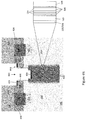

Classifications
-
- H—ELECTRICITY
- H10—SEMICONDUCTOR DEVICES; ELECTRIC SOLID-STATE DEVICES NOT OTHERWISE PROVIDED FOR
- H10D—INORGANIC ELECTRIC SEMICONDUCTOR DEVICES
- H10D62/00—Semiconductor bodies, or regions thereof, of devices having potential barriers
- H10D62/10—Shapes, relative sizes or dispositions of the regions of the semiconductor bodies; Shapes of the semiconductor bodies
- H10D62/102—Constructional design considerations for preventing surface leakage or controlling electric field concentration
- H10D62/103—Constructional design considerations for preventing surface leakage or controlling electric field concentration for increasing or controlling the breakdown voltage of reverse-biased devices
- H10D62/105—Constructional design considerations for preventing surface leakage or controlling electric field concentration for increasing or controlling the breakdown voltage of reverse-biased devices by having particular doping profiles, shapes or arrangements of PN junctions; by having supplementary regions, e.g. junction termination extension [JTE]
- H10D62/109—Reduced surface field [RESURF] PN junction structures
- H10D62/111—Multiple RESURF structures, e.g. double RESURF or 3D-RESURF structures
-
- H—ELECTRICITY
- H10—SEMICONDUCTOR DEVICES; ELECTRIC SOLID-STATE DEVICES NOT OTHERWISE PROVIDED FOR
- H10D—INORGANIC ELECTRIC SEMICONDUCTOR DEVICES
- H10D12/00—Bipolar devices controlled by the field effect, e.g. insulated-gate bipolar transistors [IGBT]
- H10D12/411—Insulated-gate bipolar transistors [IGBT]
- H10D12/441—Vertical IGBTs
- H10D12/461—Vertical IGBTs having non-planar surfaces, e.g. having trenches, recesses or pillars in the surfaces of the emitter, base or collector regions
- H10D12/481—Vertical IGBTs having non-planar surfaces, e.g. having trenches, recesses or pillars in the surfaces of the emitter, base or collector regions having gate structures on slanted surfaces, on vertical surfaces, or in grooves, e.g. trench gate IGBTs
-
- H—ELECTRICITY
- H10—SEMICONDUCTOR DEVICES; ELECTRIC SOLID-STATE DEVICES NOT OTHERWISE PROVIDED FOR
- H10D—INORGANIC ELECTRIC SEMICONDUCTOR DEVICES
- H10D30/00—Field-effect transistors [FET]
- H10D30/01—Manufacture or treatment
- H10D30/021—Manufacture or treatment of FETs having insulated gates [IGFET]
- H10D30/027—Manufacture or treatment of FETs having insulated gates [IGFET] of lateral single-gate IGFETs
-
- H—ELECTRICITY
- H10—SEMICONDUCTOR DEVICES; ELECTRIC SOLID-STATE DEVICES NOT OTHERWISE PROVIDED FOR
- H10D—INORGANIC ELECTRIC SEMICONDUCTOR DEVICES
- H10D30/00—Field-effect transistors [FET]
- H10D30/01—Manufacture or treatment
- H10D30/021—Manufacture or treatment of FETs having insulated gates [IGFET]
- H10D30/028—Manufacture or treatment of FETs having insulated gates [IGFET] of double-diffused metal oxide semiconductor [DMOS] FETs
- H10D30/0291—Manufacture or treatment of FETs having insulated gates [IGFET] of double-diffused metal oxide semiconductor [DMOS] FETs of vertical DMOS [VDMOS] FETs
-
- H—ELECTRICITY
- H10—SEMICONDUCTOR DEVICES; ELECTRIC SOLID-STATE DEVICES NOT OTHERWISE PROVIDED FOR
- H10D—INORGANIC ELECTRIC SEMICONDUCTOR DEVICES
- H10D30/00—Field-effect transistors [FET]
- H10D30/01—Manufacture or treatment
- H10D30/021—Manufacture or treatment of FETs having insulated gates [IGFET]
- H10D30/028—Manufacture or treatment of FETs having insulated gates [IGFET] of double-diffused metal oxide semiconductor [DMOS] FETs
- H10D30/0291—Manufacture or treatment of FETs having insulated gates [IGFET] of double-diffused metal oxide semiconductor [DMOS] FETs of vertical DMOS [VDMOS] FETs
- H10D30/0297—Manufacture or treatment of FETs having insulated gates [IGFET] of double-diffused metal oxide semiconductor [DMOS] FETs of vertical DMOS [VDMOS] FETs using recessing of the gate electrodes, e.g. to form trench gate electrodes
-
- H—ELECTRICITY
- H10—SEMICONDUCTOR DEVICES; ELECTRIC SOLID-STATE DEVICES NOT OTHERWISE PROVIDED FOR
- H10D—INORGANIC ELECTRIC SEMICONDUCTOR DEVICES
- H10D30/00—Field-effect transistors [FET]
- H10D30/60—Insulated-gate field-effect transistors [IGFET]
-
- H—ELECTRICITY
- H10—SEMICONDUCTOR DEVICES; ELECTRIC SOLID-STATE DEVICES NOT OTHERWISE PROVIDED FOR
- H10D—INORGANIC ELECTRIC SEMICONDUCTOR DEVICES
- H10D30/00—Field-effect transistors [FET]
- H10D30/60—Insulated-gate field-effect transistors [IGFET]
- H10D30/64—Double-diffused metal-oxide semiconductor [DMOS] FETs
- H10D30/66—Vertical DMOS [VDMOS] FETs
- H10D30/668—Vertical DMOS [VDMOS] FETs having trench gate electrodes, e.g. UMOS transistors
-
- H—ELECTRICITY
- H10—SEMICONDUCTOR DEVICES; ELECTRIC SOLID-STATE DEVICES NOT OTHERWISE PROVIDED FOR
- H10D—INORGANIC ELECTRIC SEMICONDUCTOR DEVICES
- H10D30/00—Field-effect transistors [FET]
- H10D30/60—Insulated-gate field-effect transistors [IGFET]
- H10D30/67—Thin-film transistors [TFT]
- H10D30/6704—Thin-film transistors [TFT] having supplementary regions or layers in the thin films or in the insulated bulk substrates for controlling properties of the device
-
- H—ELECTRICITY
- H10—SEMICONDUCTOR DEVICES; ELECTRIC SOLID-STATE DEVICES NOT OTHERWISE PROVIDED FOR
- H10D—INORGANIC ELECTRIC SEMICONDUCTOR DEVICES
- H10D62/00—Semiconductor bodies, or regions thereof, of devices having potential barriers
- H10D62/01—Manufacture or treatment
- H10D62/051—Forming charge compensation regions, e.g. superjunctions
- H10D62/052—Forming charge compensation regions, e.g. superjunctions by forming stacked epitaxial layers
-
- H—ELECTRICITY
- H10—SEMICONDUCTOR DEVICES; ELECTRIC SOLID-STATE DEVICES NOT OTHERWISE PROVIDED FOR
- H10D—INORGANIC ELECTRIC SEMICONDUCTOR DEVICES
- H10D62/00—Semiconductor bodies, or regions thereof, of devices having potential barriers
- H10D62/10—Shapes, relative sizes or dispositions of the regions of the semiconductor bodies; Shapes of the semiconductor bodies
- H10D62/113—Isolations within a component, i.e. internal isolations
-
- H—ELECTRICITY
- H10—SEMICONDUCTOR DEVICES; ELECTRIC SOLID-STATE DEVICES NOT OTHERWISE PROVIDED FOR
- H10D—INORGANIC ELECTRIC SEMICONDUCTOR DEVICES
- H10D62/00—Semiconductor bodies, or regions thereof, of devices having potential barriers
- H10D62/10—Shapes, relative sizes or dispositions of the regions of the semiconductor bodies; Shapes of the semiconductor bodies
- H10D62/124—Shapes, relative sizes or dispositions of the regions of semiconductor bodies or of junctions between the regions
- H10D62/126—Top-view geometrical layouts of the regions or the junctions
- H10D62/127—Top-view geometrical layouts of the regions or the junctions of cellular field-effect devices, e.g. multicellular DMOS transistors or IGBTs
-
- H—ELECTRICITY
- H10—SEMICONDUCTOR DEVICES; ELECTRIC SOLID-STATE DEVICES NOT OTHERWISE PROVIDED FOR
- H10D—INORGANIC ELECTRIC SEMICONDUCTOR DEVICES
- H10D62/00—Semiconductor bodies, or regions thereof, of devices having potential barriers
- H10D62/10—Shapes, relative sizes or dispositions of the regions of the semiconductor bodies; Shapes of the semiconductor bodies
- H10D62/13—Semiconductor regions connected to electrodes carrying current to be rectified, amplified or switched, e.g. source or drain regions
- H10D62/149—Source or drain regions of field-effect devices
- H10D62/151—Source or drain regions of field-effect devices of IGFETs
- H10D62/152—Source regions of DMOS transistors
- H10D62/154—Dispositions
-
- H—ELECTRICITY
- H10—SEMICONDUCTOR DEVICES; ELECTRIC SOLID-STATE DEVICES NOT OTHERWISE PROVIDED FOR
- H10D—INORGANIC ELECTRIC SEMICONDUCTOR DEVICES
- H10D62/00—Semiconductor bodies, or regions thereof, of devices having potential barriers
- H10D62/10—Shapes, relative sizes or dispositions of the regions of the semiconductor bodies; Shapes of the semiconductor bodies
- H10D62/13—Semiconductor regions connected to electrodes carrying current to be rectified, amplified or switched, e.g. source or drain regions
- H10D62/149—Source or drain regions of field-effect devices
- H10D62/151—Source or drain regions of field-effect devices of IGFETs
- H10D62/156—Drain regions of DMOS transistors
- H10D62/158—Dispositions
-
- H—ELECTRICITY
- H10—SEMICONDUCTOR DEVICES; ELECTRIC SOLID-STATE DEVICES NOT OTHERWISE PROVIDED FOR
- H10D—INORGANIC ELECTRIC SEMICONDUCTOR DEVICES
- H10D62/00—Semiconductor bodies, or regions thereof, of devices having potential barriers
- H10D62/10—Shapes, relative sizes or dispositions of the regions of the semiconductor bodies; Shapes of the semiconductor bodies
- H10D62/17—Semiconductor regions connected to electrodes not carrying current to be rectified, amplified or switched, e.g. channel regions
- H10D62/393—Body regions of DMOS transistors or IGBTs
-
- H—ELECTRICITY
- H10—SEMICONDUCTOR DEVICES; ELECTRIC SOLID-STATE DEVICES NOT OTHERWISE PROVIDED FOR
- H10D—INORGANIC ELECTRIC SEMICONDUCTOR DEVICES
- H10D64/00—Electrodes of devices having potential barriers
- H10D64/20—Electrodes characterised by their shapes, relative sizes or dispositions
- H10D64/23—Electrodes carrying the current to be rectified, amplified, oscillated or switched, e.g. sources, drains, anodes or cathodes
- H10D64/251—Source or drain electrodes for field-effect devices
- H10D64/252—Source or drain electrodes for field-effect devices for vertical or pseudo-vertical devices
- H10D64/2527—Source or drain electrodes for field-effect devices for vertical or pseudo-vertical devices for vertical devices wherein the source or drain electrodes are recessed in semiconductor bodies
-
- H—ELECTRICITY
- H10—SEMICONDUCTOR DEVICES; ELECTRIC SOLID-STATE DEVICES NOT OTHERWISE PROVIDED FOR
- H10D—INORGANIC ELECTRIC SEMICONDUCTOR DEVICES
- H10D64/00—Electrodes of devices having potential barriers
- H10D64/20—Electrodes characterised by their shapes, relative sizes or dispositions
- H10D64/27—Electrodes not carrying the current to be rectified, amplified, oscillated or switched, e.g. gates
- H10D64/311—Gate electrodes for field-effect devices
- H10D64/411—Gate electrodes for field-effect devices for FETs
- H10D64/511—Gate electrodes for field-effect devices for FETs for IGFETs
- H10D64/512—Disposition of the gate electrodes, e.g. buried gates
- H10D64/513—Disposition of the gate electrodes, e.g. buried gates within recesses in the substrate, e.g. trench gates, groove gates or buried gates
-
- H—ELECTRICITY
- H10—SEMICONDUCTOR DEVICES; ELECTRIC SOLID-STATE DEVICES NOT OTHERWISE PROVIDED FOR
- H10P—GENERIC PROCESSES OR APPARATUS FOR THE MANUFACTURE OR TREATMENT OF DEVICES COVERED BY CLASS H10
- H10P14/00—Formation of materials, e.g. in the shape of layers or pillars
- H10P14/60—Formation of materials, e.g. in the shape of layers or pillars of insulating materials
- H10P14/63—Formation of materials, e.g. in the shape of layers or pillars of insulating materials characterised by the formation processes
- H10P14/6326—Deposition processes
- H10P14/6349—Deposition of epitaxial materials
-
- H—ELECTRICITY
- H10—SEMICONDUCTOR DEVICES; ELECTRIC SOLID-STATE DEVICES NOT OTHERWISE PROVIDED FOR
- H10P—GENERIC PROCESSES OR APPARATUS FOR THE MANUFACTURE OR TREATMENT OF DEVICES COVERED BY CLASS H10
- H10P14/00—Formation of materials, e.g. in the shape of layers or pillars
- H10P14/60—Formation of materials, e.g. in the shape of layers or pillars of insulating materials
- H10P14/69—Inorganic materials
- H10P14/6903—Inorganic materials containing silicon
-
- H—ELECTRICITY
- H10—SEMICONDUCTOR DEVICES; ELECTRIC SOLID-STATE DEVICES NOT OTHERWISE PROVIDED FOR
- H10P—GENERIC PROCESSES OR APPARATUS FOR THE MANUFACTURE OR TREATMENT OF DEVICES COVERED BY CLASS H10
- H10P50/00—Etching of wafers, substrates or parts of devices
- H10P50/20—Dry etching; Plasma etching; Reactive-ion etching
- H10P50/28—Dry etching; Plasma etching; Reactive-ion etching of insulating materials
- H10P50/282—Dry etching; Plasma etching; Reactive-ion etching of insulating materials of inorganic materials
- H10P50/283—Dry etching; Plasma etching; Reactive-ion etching of insulating materials of inorganic materials by chemical means
-
- H—ELECTRICITY
- H10—SEMICONDUCTOR DEVICES; ELECTRIC SOLID-STATE DEVICES NOT OTHERWISE PROVIDED FOR
- H10P—GENERIC PROCESSES OR APPARATUS FOR THE MANUFACTURE OR TREATMENT OF DEVICES COVERED BY CLASS H10
- H10P95/00—Generic processes or apparatus for manufacture or treatments not covered by the other groups of this subclass
- H10P95/90—Thermal treatments, e.g. annealing or sintering
-
- H—ELECTRICITY
- H10—SEMICONDUCTOR DEVICES; ELECTRIC SOLID-STATE DEVICES NOT OTHERWISE PROVIDED FOR
- H10W—GENERIC PACKAGES, INTERCONNECTIONS, CONNECTORS OR OTHER CONSTRUCTIONAL DETAILS OF DEVICES COVERED BY CLASS H10
- H10W20/00—Interconnections in chips, wafers or substrates
- H10W20/01—Manufacture or treatment
- H10W20/071—Manufacture or treatment of dielectric parts thereof
- H10W20/074—Manufacture or treatment of dielectric parts thereof of dielectric parts comprising thin functional dielectric layers, e.g. dielectric etch-stop, barrier, capping or liner layers
-
- H—ELECTRICITY
- H10—SEMICONDUCTOR DEVICES; ELECTRIC SOLID-STATE DEVICES NOT OTHERWISE PROVIDED FOR
- H10D—INORGANIC ELECTRIC SEMICONDUCTOR DEVICES
- H10D12/00—Bipolar devices controlled by the field effect, e.g. insulated-gate bipolar transistors [IGBT]
- H10D12/411—Insulated-gate bipolar transistors [IGBT]
- H10D12/441—Vertical IGBTs
-
- H—ELECTRICITY
- H10—SEMICONDUCTOR DEVICES; ELECTRIC SOLID-STATE DEVICES NOT OTHERWISE PROVIDED FOR
- H10D—INORGANIC ELECTRIC SEMICONDUCTOR DEVICES
- H10D12/00—Bipolar devices controlled by the field effect, e.g. insulated-gate bipolar transistors [IGBT]
- H10D12/411—Insulated-gate bipolar transistors [IGBT]
- H10D12/441—Vertical IGBTs
- H10D12/461—Vertical IGBTs having non-planar surfaces, e.g. having trenches, recesses or pillars in the surfaces of the emitter, base or collector regions
-
- H—ELECTRICITY
- H10—SEMICONDUCTOR DEVICES; ELECTRIC SOLID-STATE DEVICES NOT OTHERWISE PROVIDED FOR
- H10D—INORGANIC ELECTRIC SEMICONDUCTOR DEVICES
- H10D62/00—Semiconductor bodies, or regions thereof, of devices having potential barriers
- H10D62/10—Shapes, relative sizes or dispositions of the regions of the semiconductor bodies; Shapes of the semiconductor bodies
- H10D62/102—Constructional design considerations for preventing surface leakage or controlling electric field concentration
- H10D62/103—Constructional design considerations for preventing surface leakage or controlling electric field concentration for increasing or controlling the breakdown voltage of reverse-biased devices
- H10D62/105—Constructional design considerations for preventing surface leakage or controlling electric field concentration for increasing or controlling the breakdown voltage of reverse-biased devices by having particular doping profiles, shapes or arrangements of PN junctions; by having supplementary regions, e.g. junction termination extension [JTE]
- H10D62/106—Constructional design considerations for preventing surface leakage or controlling electric field concentration for increasing or controlling the breakdown voltage of reverse-biased devices by having particular doping profiles, shapes or arrangements of PN junctions; by having supplementary regions, e.g. junction termination extension [JTE] having supplementary regions doped oppositely to or in rectifying contact with regions of the semiconductor bodies, e.g. guard rings with PN or Schottky junctions
- H10D62/107—Buried supplementary regions, e.g. buried guard rings
-
- H—ELECTRICITY
- H10—SEMICONDUCTOR DEVICES; ELECTRIC SOLID-STATE DEVICES NOT OTHERWISE PROVIDED FOR
- H10D—INORGANIC ELECTRIC SEMICONDUCTOR DEVICES
- H10D62/00—Semiconductor bodies, or regions thereof, of devices having potential barriers
- H10D62/10—Shapes, relative sizes or dispositions of the regions of the semiconductor bodies; Shapes of the semiconductor bodies
- H10D62/113—Isolations within a component, i.e. internal isolations
- H10D62/115—Dielectric isolations, e.g. air gaps
Definitions
- Superjunction power MOSFETs metal-oxide-semiconductor field effect transistors
- FOM conduction loss figure of merit
- out diffusion of the p-type dopant species from the p-type pillars defines the pitch of the device, and therefore the conduction loss FOM.
- the out diffusion of the p-type dopant species from the p-type pillars also defines the thickness and number of epitaxial foundation layers used to form the superjunction structure and therefore cost.
- the n-type and p-type dopants are typically introduced simultaneously and during out diffusion, the fast-diffusing dopants define one doping zone. In the other doping zone, the fast-diffusing dopants act as background doping and therefore reduce carrier mobility.
- the semiconductor device comprises: a source region and a drain region of a first conductivity type; a body region of a second conductivity type between the source region and the drain region; a gate configured to control current through a channel of the body region; a drift zone of the first conductivity type between the body region and the drain region; a superjunction structure formed by a plurality of regions of the second conductivity type laterally spaced apart from one another by intervening regions of the drift zone; and a diffusion barrier structure disposed along sidewalls of the regions of the second conductivity type of the superjunction structure, the diffusion barrier structure comprising alternating layers of Si and oxygen-doped Si and a Si capping layer on the alternating layers of Si and oxygen-doped Si.
- the diffusion barrier structure may also be disposed along a bottom face of the regions of the second conductivity type.
- the drift zone may contact a bottom face of the regions of the second conductivity type.
- the drain region may be formed in a Si substrate, the drift zone may be disposed in a first Si epitaxial layer formed over the Si substrate, and the source region and the body region may be disposed in a second Si epitaxial layer formed over the first Si epitaxial layer.
- the gate may be a trench gate formed in the second Si epitaxial layer or a planar gate formed on a surface of the second Si epitaxial layer facing away from the first Si epitaxial layer.
- the semiconductor device may further comprise a contact in electrical contact with the source region and the body region in the second Si epitaxial layer.
- the contact may vertically extend through the second Si epitaxial layer, into the first Si epitaxial layer and electrically contacts a region of the plurality of regions of the second conductivity type, and sidewalls of the contact may be laterally separated from the second Si epitaxial layer and the first Si epitaxial layer by an insulating material.
- the second Si epitaxial layer may contact a top face of the regions of the second conductivity type.
- the method comprises: forming a source region and a drain region of a first conductivity type; forming a body region of a second conductivity type, wherein the body region is disposed between the source region and the drain region; forming a gate configured to control current through a channel of the body region; forming a drift zone of the first conductivity type, wherein the drift zone is disposed between the body region and the drain region; forming a plurality of regions of the second conductivity type laterally spaced apart from one another by intervening regions of the drift zone, to form a superjunction structure; and forming a diffusion barrier structure along sidewalls of the regions of the second conductivity type of the superjunction structure, the diffusion barrier structure comprising alternating layers of Si and oxygen-doped Si and a Si capping layer on the alternating layers of Si and oxygen-doped Si.
- Forming the plurality of regions of the second conductivity type and forming the diffusion barrier structure along sidewalls of the regions of the second conductivity type may comprise: etching a plurality of trenches in a first Si epitaxial layer of the first conductivity type, wherein the first Si epitaxial layer includes the drift zone; epitaxially growing the alternating layers of Si and oxygen-doped Si on sidewalls and a bottom of the trenches; epitaxially growing the Si capping layer on the alternating layers of Si and oxygen-doped Si; and after forming the diffusion barrier structure, filling the trenches with epitaxial Si of the second conductivity type.
- forming the source region and the body region may comprise: after filling the trenches with the epitaxial Si of the second conductivity type, forming a second Si epitaxial layer over the first Si epitaxial layer; implanting dopant species of the first conductivity type into a first part of the second Si epitaxial layer which corresponds to the source region; implanting dopant species of the second conductivity type into a second part of the second Si epitaxial layer which corresponds to the body region; and annealing the second Si epitaxial layer to activate the implanted dopant species of the first conductivity type to form the source region and to activate the implanted dopant species of the second conductivity type to form the body region.
- the drain region may be disposed in a Si substrate over which the first Si epitaxial layer is formed.
- the second Si epitaxial layer may be annealed in a temperature range above 1000 °C for 30 minutes or less.
- the method may further comprise planarizing the epitaxial Si of the second conductivity type before forming the second Si epitaxial layer.
- the method may further comprise: etching a contact trench into the second Si epitaxial layer, the contact trench exposing a sidewall of the source region and a top surface of the body region; and filling the contact trench with an electrically conductive material which contacts the sidewall of the source region and the top surface of the body region.
- etching the contact trench may further comprise: etching the contact trench into the first Si epitaxial layer to expose a sidewall of the first Si epitaxial layer; depositing an insulating material on the sidewall of the body region and the sidewall of the first Si epitaxial layer; and etching the contact trench into a region of the plurality of regions of the second conductivity type, wherein the electrically conductive material may be in contact with the region of the second conductivity type into which the contact trench is etched, wherein sidewalls of the electrically conductive material may be laterally separated from the second Si epitaxial layer and the first Si epitaxial layer by the insulating material.
- the method may further comprise removing the alternating layers of Si and oxygen-doped Si and the Si capping layer from the bottom of the plurality of trenches before filling the plurality of trenches with the epitaxial Si of the second conductivity type, so that the bottom of the plurality of trenches is uncovered when the plurality of trenches is filled with the epitaxial Si of the second conductivity type.
- filling the plurality of trenches with the epitaxial Si of the second conductivity type may comprise: selectively growing in situ doped epitaxial Si of the second conductivity type in the plurality of trenches; and planarizing the in situ doped epitaxial Si of the second conductivity type before forming the second Si epitaxial layer.
- filling the plurality of trenches with the epitaxial Si of the second conductivity type may comprise: selectively growing epitaxial Si in the plurality of trenches; planarizing the epitaxial Si; implanting dopant species of the second conductivity type into the planarized epitaxial Si; and annealing the first Si epitaxial layer to activate the implanted dopant species of the second conductivity type.
- Embodiments described herein provide a diffusion barrier structure between p-type and n-type pillars of a superjunction structure of a semiconductor device.
- the diffusion barrier structure controls dopant interdiffusion from both lateral (side) directions in the superjunction region of the device, thereby improving superjunction device performance e.g. by reducing cell pitch.
- the cell pitch may be a center-to-center distance of neighboring cells or an edge-to-edge distance.
- the diffusion barrier structure described herein provides tighter dopant distribution control in the superjunction region of a semiconductor device.
- the conduction loss FOM given by Rdson*A may be reduced by about 20% or more by cutting in half the amount of n-type and p-type dopant interdiffusion in the superjunction region of a small pitch device, allowing superjunction-based transistors to be used in low voltage ranges e.g. as low as 10V.
- the diffusion barrier structure teachings described herein are also well-suited for high voltage applications, e.g., up to 1000V or even higher. Described next in more detail are embodiments of semiconductor devices with such a diffusion barrier structure, and corresponding methods of manufacture.
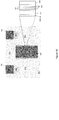
- Figure 1 illustrates a partial cross-sectional view of an embodiment of one cell of a semiconductor device 100 having a superjunction structure.
- the semiconductor device 100 may include a plurality of such cells, each cell having the same or similar construction.
- the semiconductor device 100 may be a power semiconductor device such as a power MOSFET, an IGBT (insulated gate bipolar transistor), etc.
- the semiconductor device includes a source region 102 and a drain region 104 of a first conductivity type, a body region 106 of a second conductivity type opposite the first conductivity type between the source region 102 and the drain region 104, a planar gate 108 which includes a gate electrode 110 separated from the underlying semiconductor material by a gate dielectric 112 and configured to control current through a channel 114 of the body region 106, and a drift zone 116 of the first conductivity type between the body region 106 and the drain region 104.
- the channel region 114 laterally extends along the bottom of the planar gate 108.
- the device current has a lateral component in the channel region 114 along the planar gate lateral extension, and a vertical component along the drift zone vertical extension.
- additional structures may be formed in the drift zone 116 and/or between the drift zone 116 and the drain region 104.
- a field stop layer (not shown) may be formed between the drift zone 116 and the drain region 104 in the case of an IGBT type device.
- any type of semiconductor device with a superjunction structure may utilize the diffusion barrier teachings described herein.
- the source region 102, drain region 104 and drift zone 116 are doped n-type and the body region 106 and channel region 114 are doped p-type.
- the source region 102, drain region 104 and drift zone 116 are doped p-type and the body region 106 and channel region 114 are doped n-type.
- the superjunction structure is formed by a plurality of regions 118 of the second conductivity type laterally spaced apart from one another by intervening regions 120 of the drift zone 116.
- the regions 118 of the second conductivity type may have a columnar (vertically elongated) shape, a stripe (laterally elongated) shape, or another type of shape depending on the type of cell construction. Two such regions 118 of the second conductivity type and one intervening region 120 of the drift zone 116 are shown in the partial cross-sectional view of the semiconductor device 100 in Figure 1 .
- the drain region 104 of the semiconductor device 100 is a highly doped region of a semiconductor substrate such as a Si substrate and the drift zone 116 and the regions 118 of the second conductivity type are part of a first epitaxial layer formed over the semiconductor substrate. Further according to this embodiment, the source region 102 and the body region 106 of the semiconductor device 100 are disposed in a second epitaxial layer formed over the first epitaxial layer.
- the semiconductor device 100 may also include a contact trench 122 which extends through the source region 102 and into the body region 106.
- the contact trench 122 is filled with an electrically conductive material 124 such as doped polysilicon, metal, etc. which contacts the source region 102 at the sidewall of the contact trench 122 and a highly doped body contact region 126 at the bottom of the contact trench 122.
- the highly doped body contact region 126 has the same doping type as the body region 106, but at a higher concentration to provide good ohmic contact with the electrically conductive material 124 which fills the contact trench 122.
- the planar gate 108 is separated from the overlying electrically conductive material 124 by an interlayer dielectric 128.
- the semiconductor device 100 further includes a diffusion barrier structure 130 disposed along at least sidewalls 132 of the regions 118 of the second conductivity type of the superjunction structure.
- the diffusion barrier structure 130 is also disposed along the bottom face 133 of the regions 118 of the second conductivity type.
- the diffusion barrier structure 130 comprises alternating layers of Si 134 and oxygen-doped Si 136 and a Si capping layer 138 on the alternating layers of Si 134 and oxygen-doped Si 136.
- the oxygen-doped Si layers 136 have a very high oxygen dopant concentration within respective monolayers 136, each of which adjoins a Si layer 134 which may be of a different thickness than the adjoining oxygen-doped Si layer 136.
- the alternating layers of Si 134 and oxygen-doped Si form 136 an oxygen-doped silicon region grown by epitaxy.
- the oxygen concentration for each oxygen-doped Si layer 136 is below 5e14cm-3.
- Each oxygen-doped Si layer 136 may have a thickness in the atomic range (e.g. one or several atoms thick) or in the nanometer (nm) range to ensure sufficient crystal information for growing Si 134 on the oxygen-doped Si layers 136.
- the alternating layers of Si 134 and oxygen-doped Si 136 may be realized by epitaxially growing Si layers 134 alternating with oxygen layers 136 respectively adsorbed on surfaces of the Si layers 134, e.g., with a particular limited thickness for the oxygen-doped Si layers 136 to ensure adequate Si growth.
- Figure 1 provides an exploded view of the diffusion barrier structure 130, which may also include a Si buffer layer 140 below the alternating layers of Si 134 and oxygen-doped Si 136.
- the Si buffer layer 140 may be relatively thin, e.g., in the range of 2-5 nm thick.
- the Si buffer layer 140 may be grown after an implant or an etch step.
- the capping layer 138 provides high carrier mobility in this region of the device 100.
- Part of the channel region 114 may be formed in the part of the Si capping layer 138 which laterally extends along the planar gate 108.
- the buffer layer 140 may be omitted.
- the oxygen-doped Si layers 136 of the diffusion barrier structure 130 limit lateral out-diffusion of dopant atoms from the regions 118 of the second conductivity type of the superjunction structure into the intervening regions 120 of the drift zone 116, and are especially effective at limiting interstitial-driven diffusion as the oxygen acts as an interstitial stop.
- the lateral dimension of the regions 118 of the second conductivity type may be well controlled, allowing for a smaller cell pitch.
- the dopants diffuse as usual.
- dopant interdiffusion is slowed down by the diffusion barrier structure 130.
- the oxygen-doped Si layers 136 of the diffusion barrier structure 130 may also improve carrier mobility within the channel region 114 of the device 100.
- the oxygen-doped Si layers 136 of the diffusion barrier structure 130 may be formed by introducing oxygen partial monolayers to a Si lattice.
- the oxygen atoms are interstitially placed to minimize disruption to the Si lattice.
- Layers 134 of Si atoms separate adjacent oxygen partial monolayers 136.
- the alternating layers of Si 134 and oxygen-doped Si 136 may be formed by Si epitaxy with absorption of oxygen at different steps. For example, temperature and gaseous conditions can be controlled during the epitaxy process to form the partial oxygen monolayers 136.
- Oxygen may be introduced/incorporated between epitaxial layers of Si 134, e.g. by controlling the introduction of an oxygen precursor into the epitaxy chamber.
- the resulting barrier barrier structure 130 includes monolayers 136 that comprise mainly Si but have a doped level or concentration level of oxygen alternating with standard epitaxial layers 134 of Si without oxygen.
- the diffusion barrier structure 130 also comprises a capping layer 138 of Si epitaxially grown on the alternating layers of Si 134 and oxygen-doped Si 136, or the capping layer 138 of Si may be omitted.
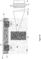
- Figure 2 illustrates a partial cross-sectional view of another embodiment of one cell of a semiconductor device 200 having a superjunction structure.
- the embodiment illustrated in Figure 2 is similar to the embodiment illustrated in Figure 1 .
- the semiconductor device 200 has a trench gate 202 instead of a planar gate.
- the trench gate 202 includes a gate trench 204 extending into the semiconductor material and a gate electrode 206 disposed in the gate trench 204.
- the gate electrode 206 is insulated from the surrounding semiconductor material by a gate dielectric 208.
- a field electrode (not shown) may be disposed in the gate trench 202 below the gate electrode 206, and insulated from the surrounding semiconductor material and the gate electrode 206 by a field dielectric (not shown).
- the field electrode instead may be disposed in a different trench than the gate electrode 206, or omitted altogether.
- the semiconductor device 200 also includes the diffusion barrier structure 130 disposed along at least sidewalls 132 of the regions 118 of the second conductivity type of the superjunction structure.
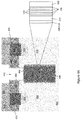
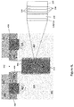
- Figures 3A through 3E illustrate respective cross-sectional views of a semiconductor device having a superjunction structure and the diffusion barrier structure 130, during different stages of an embodiment of a manufacturing process.
- Figure 3A shows the semiconductor device after a semiconductor growth substrate 300 such as a Si substrate is provided and a first epitaxial layer 302 of the first conductivity type is epitaxially grown on the substrate 300.
- the growth substrate 300 may be heavily doped, e.g., to form a drain region of the device.
- the first epitaxial layer 302 may be doped in situ or ex situ, and forms the drift zone of the device.
- Figure 3B shows the semiconductor device after trenches 304 are formed in the first epitaxial layer 302.
- the trenches 304 may be etched into the first epitaxial layer 302 using any typical trench formation process such as applying a mask / insulating material (not shown) on the front main surface 303 of the first epitaxial layer 302 and etching the trenches 304 into the first epitaxial layer 302 through respective openings in the mask.
- Figure 3C shows the semiconductor device after the alternating layers of Si 134 and oxygen-doped Si 136 of the diffusion barrier structure 130 are epitaxially grown on the sidewalls and bottom of the trenches 304.
- the alternating layers of Si 134 and oxygen-doped Si 136 are epitaxially grown on the sidewalls and the bottom of the trenches 304 after etching the trenches 304 into the first epitaxial layer 302 but before forming the source and body regions of the device.
- the capping layer 138 of Si may have the same standard in situ doping concentration as the alternating layers of Si 134 and oxygen-doped Si 136 and may be doped later with a different dopant species and concentration. Alternatively, the capping layer 138 of Si may have a different in situ doping concentration compared to the alternating layers of Si 134 and oxygen-doped Si 136.
- Figure 3D shows the semiconductor device after the trenches 304 are filled with epitaxial Si 306 of the second conductivity type.
- the epitaxial Si 306 of the second conductivity type may be doped in situ or ex situ and may be planarized, e.g. by chemical-mechanical polishing (CMP).
- CMP chemical-mechanical polishing
- Figure 3E shows the semiconductor device after dopant species of the first conductivity type are implanted into a first part of the epitaxial Si 306 of the second conductivity type or into a second Si epitaxial layer grown over the epitaxial Si 306, and after dopant species of the second conductivity type are implanted into a second (deeper) part of the epitaxial Si 306 or second epitaxial layer.
- the semiconductor device is annealed to activate the implanted dopant species of the first conductivity type to form source regions 308 of the device, and to activate the implanted dopant species of the second conductivity type to form body regions 310 of the device.
- the annealing is done in a temperature range above 1000 °C for 30 minutes or less.
- the epitaxial Si 306 of the second conductivity type may be planarized e.g. by CMP before forming the second Si epitaxial layer.
- Gate trenches 312 are also formed in the semiconductor material, and a gate electrode 314 is disposed in each gate trench 312.
- the gate electrodes 314 are insulated from the surrounding semiconductor material by a gate dielectric 316.
- Contact trenches 318 extend through the source regions 308 and into the body regions 310.
- the contact trenches 318 are filled with an electrically conductive material 320 such as doped polysilicon, metal, etc. which contacts the source regions 308 at the sidewall of the contact trenches 318 and a highly doped body contact region 322 at the bottom of the contact trenches 318.
- the highly doped body contact regions 322 have the same doping type as the body regions 310, but at a higher concentration to provide good ohmic contact with the electrically conductive material 320 which fills the contact trenches 318.
- An interlayer dielectric 324 is provided between the electrically conductive material 320 top surface of the semiconductor material.
- Figures 4A through 4O illustrate respective cross-sectional views of a semiconductor device having a superjunction structure and the diffusion barrier structure 130, during different stages of another embodiment of a manufacturing process.
- Figures 4A through 4O illustrate processing of the semiconductor device in one cell.
- the semiconductor device may include a plurality of such cells, each cell having the same or similar construction.
- Figure 4A shows the semiconductor device after a base semiconductor material 400 is provided and a hard mask 402 such as a silicon-based hard mask is formed on the base semiconductor material 400.
- the hard mask 402 has openings 404 which define the location of trenches to be etched into the base semiconductor material 400.
- the base semiconductor material 400 may be a growth substrate such as a Si substrate or a Si epitaxial layer grown over such a substrate.
- Figure 4B shows the semiconductor device after trenches 406 are etched into the base semiconductor material 400 and after the diffusion barrier structure 130 is formed along the sidewalls 408 and bottom 410 of the trenches 406.
- the diffusion barrier structure 130 may be formed as previously described herein.
- Figure 4C shows the semiconductor device after a spacer etch process which removes the diffusion barrier structure 130 from the bottom of the trenches 406.
- the base semiconductor material 400 may form the drift zone of the device and the drift zone may adjoin the bottom 410 of the trenches 406.
- the spacer etch process may be skipped so that the diffusion barrier structure 130 remains along the bottom of the trenches 406.
- Figure 4D shows the semiconductor device after selective epitaxial growth of semiconductor material 412 of the second conductivity type in the trenches 406 and on the top surface of the base semiconductor material 400.
- the semiconductor material 412 of the second conductivity type which fills the trenches 406 may be doped in situ or ex situ.
- ex situ doping e.g. if more precise doping dose control is desired, selective epitaxial growth of Si in the trenches 406 is performed followed by planarization, hard mask removal, masked dopant implantation and dopant activation to define regions 412 of the second conductivity type in the trenches 406.
- selective epitaxial growth of doped (second conductivity type) Si in the trenches 406 is performed followed by planarization and hard mask removal.
- the semiconductor material 412 filling the trenches 406 is planarized, e.g. by CMP which stops on the hard mask 402, and the hard mask 402 is removed, yielding regions 412 of the second conductivity type which are laterally spaced apart from one another by intervening regions 414 of the drift zone realized by the base semiconductor material 400.
- the regions 412 of the second conductivity type and the intervening regions 414 of the drift zone collectively form a superjunction structure as previously described herein.
- One such region 412 of the second conductivity type and two such intervening regions 414 of the drift zone are shown in the partial cross-sectional view in Figure 4D .
- the drift zone realized by the base semiconductor material 400 contacts the bottom face 416 of the regions 412 of the second conductivity type.
- Figure 4E shows the semiconductor device after a Si epitaxial layer 418 of the first conductivity type is grown over the base semiconductor material 400 of the same conductivity type.
- the Si epitaxial layer 418 of the first conductivity type may be doped in situ or ex situ.
- Figure 4F shows the semiconductor device after gate trenches 420 are etched into the Si epitaxial layer 418 of the first conductivity type, a sacrificial oxide 422 is formed on the sidewalls and bottom of the gate trenches 420, and an optional implant of the first conductivity type is performed into the bottom of the gate trenches 420 to form doped regions 424 of the first conductivity type just below the gate trenches 420.
- Figure 4G shows the semiconductor device after removal of the sacrificial oxide 422 from the sidewalls and bottom of the gate trenches 420, subsequent formation of a gate oxide 426 on the sidewalls and bottom of the gate trenches 420, and formation of gate electrode 428 in the gate trenches 420.
- the gate oxide 426 separates the gate electrodes 428 from the surrounding semiconductor material.
- Figure 4H shows the semiconductor device after a screen oxide 430 is formed on the Si epitaxial layer 418, and after dopant species of the second conductivity type are implanted and driven into a lower part 432 of the Si epitaxial layer 418 and dopant species of the first conductivity type are implanted into an upper part 434 of the Si epitaxial layer 418.
- the Si epitaxial layer 418 is eventually annealed to activate the implanted dopant species of the first conductivity type to form the source region 434' of each cell and to activate the implanted dopant species of the second conductivity type to form the body region 432' of each cell.
- the Si epitaxial layer 418 is annealed in a temperature range above 1000 °C for 30 minutes or less.
- Figure 4I shows the semiconductor device after an interlayer dielectric 436 is formed on the Si epitaxial layer 418, and after a patterned contact mask 438 such as a photoresist is formed on the interlayer dielectric.
- the patterned contact mask 438 has openings 440 aligned with the trenches 406 formed in the base semiconductor material 400.
- Figure 4J shows the semiconductor device after contact trenches 422 are etched into the Si epitaxial layer 418 and to the semiconductor material 412 of the second conductivity type which fills the trenches 406.
- the contact trench etching process etching exposes a sidewall 423 of the Si epitaxial layer 418 and of the base semiconductor material 400, and may include an anisotropic etch of the exposed part of the interlayer dielectric 436, an anisotropic etch of the exposed part of the Si epitaxial layer 418, and a lateral etch of the interlayer dielectric 436 to widen the openings formed in the interlayer dielectric 436 relative to the trenches 442 etched into the Si epitaxial layer 418.
- the patterned contact mask 438 is removed after the contact trenches 442 are formed.
- Figure 4K shows the semiconductor device after deposition of a spacer oxide 444 in the contact trenches 442.
- the spacer oxide 444 is deposited on the exposed sidewall 423 of the Si epitaxial layer 418 and of the base semiconductor material 400, and on the top surface 446 of the semiconductor material 412.
- Figure 4L shows the semiconductor device after removal of the spacer oxide 444 from the top surface 446 of the semiconductor material 412 of the second conductivity type which fills the trenches 406.
- Figure 4M shows the semiconductor device after a recess etch of the exposed top surface 446 of the semiconductor material 412 of the second conductivity type which fills the trenches 406, and after a lateral etch back of the source region 434' to create a step 448 between the source region 434' and the body region 432'.
- each contact trench 422 exposes the sidewall 450 of the adjoining source region 434' and the top surface 452 of the body region 432'.
- Figure 4N shows the semiconductor device after highly doped body contact regions 454 such as p+ regions in the case of an n-channel device are formed in the exposed top surface 452 of the body region 432' and in the recessed part of the semiconductor material 412 of the second conductivity type which fills the trenches 406.
- the highly doped body contact regions 454 provide low ohmic contact to the adjacent semiconductor material.
- the device may be annealed at this time to activate all previously implanted dopants, including the source and body region dopants.
- Figure 4O shows the semiconductor device after the contact trenches 442 are filled with an electrically conductive material 456 which contacts the sidewall 450 of the source region 434' and the top surface 452 of the body region 432'.
- the electrically conductive material 456 is formed by depositing an electrically conductive liner 458 such as a Ti or TiN liner in the contact trenches 442, subsequently filling the contact trenches with a metal 460 such as W, and planarizing the metal 460 e.g. by an etch back process.
- a metal layer 462 is then deposited on the interlayer dielectric 436 using a typical metal lithography process. The metal layer is in contact with the electrically conductive material 456 which fills the contact trenches 442.
Landscapes
- Electrodes Of Semiconductors (AREA)
- Chemical & Material Sciences (AREA)
- Composite Materials (AREA)
- Recrystallisation Techniques (AREA)
- Chemical Kinetics & Catalysis (AREA)
- General Chemical & Material Sciences (AREA)
Abstract
Description
- Superjunction power MOSFETs (metal-oxide-semiconductor field effect transistors) have alternating regions of p-type pillars and n-type pillars. Because the impurity concentration of the n-type pillar regions can be increased, the conduction loss figure of merit (FOM) given by Rdson*A can be reduced, where Rdson is the drain-source on resistance of the device and A is device area. Since the conduction loss FOM can be reduced, the active area of the device can be made smaller for the same on-resistance, thereby enabling the switching loss FOM given by Rdson*QGD to be reduced as well, where QGD is gate-drain charge.
- However, out diffusion of the p-type dopant species from the p-type pillars defines the pitch of the device, and therefore the conduction loss FOM. The out diffusion of the p-type dopant species from the p-type pillars also defines the thickness and number of epitaxial foundation layers used to form the superjunction structure and therefore cost. In the case of multiple epitaxial foundation layers used to form a superjunction structure, the n-type and p-type dopants are typically introduced simultaneously and during out diffusion, the fast-diffusing dopants define one doping zone. In the other doping zone, the fast-diffusing dopants act as background doping and therefore reduce carrier mobility.
- Hence, better control of dopant out-diffusion in the superjunction region of a power semiconductor device is desirable.
- According to an embodiment of a semiconductor device, the semiconductor device comprises: a source region and a drain region of a first conductivity type; a body region of a second conductivity type between the source region and the drain region; a gate configured to control current through a channel of the body region; a drift zone of the first conductivity type between the body region and the drain region; a superjunction structure formed by a plurality of regions of the second conductivity type laterally spaced apart from one another by intervening regions of the drift zone; and a diffusion barrier structure disposed along sidewalls of the regions of the second conductivity type of the superjunction structure, the diffusion barrier structure comprising alternating layers of Si and oxygen-doped Si and a Si capping layer on the alternating layers of Si and oxygen-doped Si.
- The diffusion barrier structure may also be disposed along a bottom face of the regions of the second conductivity type.
- Separately or in combination, the drift zone may contact a bottom face of the regions of the second conductivity type.
- Separately or in combination, the drain region may be formed in a Si substrate, the drift zone may be disposed in a first Si epitaxial layer formed over the Si substrate, and the source region and the body region may be disposed in a second Si epitaxial layer formed over the first Si epitaxial layer.
- Separately or in combination, the gate may be a trench gate formed in the second Si epitaxial layer or a planar gate formed on a surface of the second Si epitaxial layer facing away from the first Si epitaxial layer.
- Separately or in combination, the semiconductor device may further comprise a contact in electrical contact with the source region and the body region in the second Si epitaxial layer.
- Separately or in combination, the contact may vertically extend through the second Si epitaxial layer, into the first Si epitaxial layer and electrically contacts a region of the plurality of regions of the second conductivity type, and sidewalls of the contact may be laterally separated from the second Si epitaxial layer and the first Si epitaxial layer by an insulating material.
- Separately or in combination, the second Si epitaxial layer may contact a top face of the regions of the second conductivity type.
- According to an embodiment of a method of manufacturing a semiconductor device, the method comprises: forming a source region and a drain region of a first conductivity type; forming a body region of a second conductivity type, wherein the body region is disposed between the source region and the drain region; forming a gate configured to control current through a channel of the body region; forming a drift zone of the first conductivity type, wherein the drift zone is disposed between the body region and the drain region; forming a plurality of regions of the second conductivity type laterally spaced apart from one another by intervening regions of the drift zone, to form a superjunction structure; and forming a diffusion barrier structure along sidewalls of the regions of the second conductivity type of the superjunction structure, the diffusion barrier structure comprising alternating layers of Si and oxygen-doped Si and a Si capping layer on the alternating layers of Si and oxygen-doped Si.
- Forming the plurality of regions of the second conductivity type and forming the diffusion barrier structure along sidewalls of the regions of the second conductivity type may comprise: etching a plurality of trenches in a first Si epitaxial layer of the first conductivity type, wherein the first Si epitaxial layer includes the drift zone; epitaxially growing the alternating layers of Si and oxygen-doped Si on sidewalls and a bottom of the trenches; epitaxially growing the Si capping layer on the alternating layers of Si and oxygen-doped Si; and after forming the diffusion barrier structure, filling the trenches with epitaxial Si of the second conductivity type.
- Separately or in combination, forming the source region and the body region may comprise: after filling the trenches with the epitaxial Si of the second conductivity type, forming a second Si epitaxial layer over the first Si epitaxial layer; implanting dopant species of the first conductivity type into a first part of the second Si epitaxial layer which corresponds to the source region; implanting dopant species of the second conductivity type into a second part of the second Si epitaxial layer which corresponds to the body region; and annealing the second Si epitaxial layer to activate the implanted dopant species of the first conductivity type to form the source region and to activate the implanted dopant species of the second conductivity type to form the body region.
- Separately or in combination, the drain region may be disposed in a Si substrate over which the first Si epitaxial layer is formed.
- Separately or in combination, the second Si epitaxial layer may be annealed in a temperature range above 1000 °C for 30 minutes or less.
- Separately or in combination, the method may further comprise planarizing the epitaxial Si of the second conductivity type before forming the second Si epitaxial layer.
- Separately or in combination, the method may further comprise: etching a contact trench into the second Si epitaxial layer, the contact trench exposing a sidewall of the source region and a top surface of the body region; and filling the contact trench with an electrically conductive material which contacts the sidewall of the source region and the top surface of the body region.
- Separately or in combination, etching the contact trench may further comprise: etching the contact trench into the first Si epitaxial layer to expose a sidewall of the first Si epitaxial layer; depositing an insulating material on the sidewall of the body region and the sidewall of the first Si epitaxial layer; and etching the contact trench into a region of the plurality of regions of the second conductivity type, wherein the electrically conductive material may be in contact with the region of the second conductivity type into which the contact trench is etched, wherein sidewalls of the electrically conductive material may be laterally separated from the second Si epitaxial layer and the first Si epitaxial layer by the insulating material.
- Separately or in combination, the method may further comprise removing the alternating layers of Si and oxygen-doped Si and the Si capping layer from the bottom of the plurality of trenches before filling the plurality of trenches with the epitaxial Si of the second conductivity type, so that the bottom of the plurality of trenches is uncovered when the plurality of trenches is filled with the epitaxial Si of the second conductivity type.
- Separately or in combination, filling the plurality of trenches with the epitaxial Si of the second conductivity type may comprise: selectively growing in situ doped epitaxial Si of the second conductivity type in the plurality of trenches; and planarizing the in situ doped epitaxial Si of the second conductivity type before forming the second Si epitaxial layer.
- Separately or in combination, filling the plurality of trenches with the epitaxial Si of the second conductivity type may comprise: selectively growing epitaxial Si in the plurality of trenches; planarizing the epitaxial Si; implanting dopant species of the second conductivity type into the planarized epitaxial Si; and annealing the first Si epitaxial layer to activate the implanted dopant species of the second conductivity type.
- Those skilled in the art will recognize additional features and advantages upon reading the following detailed description, and upon viewing the accompanying drawings.
- The elements of the drawings are not necessarily to scale relative to each other. Like reference numerals designate corresponding similar parts. The features of the various illustrated embodiments may be combined unless they exclude each other. Embodiments are depicted in the drawings and are detailed in the description which follows.
-
Figure 1 illustrates a partial cross-sectional view of an embodiment of one cell of a semiconductor device having a superjunction structure and a diffusion barrier structure. -
Figure 2 illustrates a partial cross-sectional view of another embodiment of one cell of a semiconductor device having a superjunction structure and a diffusion barrier structure. -
Figures 3A through 3E illustrate respective cross-sectional views of a semiconductor device having a superjunction structure and a diffusion barrier structure, during different stages of an embodiment of a manufacturing process. -
Figures 4A through 4O illustrate respective cross-sectional views of a semiconductor device having a superjunction structure and a diffusion barrier structure, during different stages of another embodiment of a manufacturing process. - Embodiments described herein provide a diffusion barrier structure between p-type and n-type pillars of a superjunction structure of a semiconductor device. The diffusion barrier structure controls dopant interdiffusion from both lateral (side) directions in the superjunction region of the device, thereby improving superjunction device performance e.g. by reducing cell pitch. The cell pitch may be a center-to-center distance of neighboring cells or an edge-to-edge distance. In each case, the diffusion barrier structure described herein provides tighter dopant distribution control in the superjunction region of a semiconductor device. As a result, the conduction loss FOM given by Rdson*A may be reduced by about 20% or more by cutting in half the amount of n-type and p-type dopant interdiffusion in the superjunction region of a small pitch device, allowing superjunction-based transistors to be used in low voltage ranges e.g. as low as 10V. The diffusion barrier structure teachings described herein are also well-suited for high voltage applications, e.g., up to 1000V or even higher. Described next in more detail are embodiments of semiconductor devices with such a diffusion barrier structure, and corresponding methods of manufacture.
-
Figure 1 illustrates a partial cross-sectional view of an embodiment of one cell of asemiconductor device 100 having a superjunction structure. Thesemiconductor device 100 may include a plurality of such cells, each cell having the same or similar construction. Thesemiconductor device 100 may be a power semiconductor device such as a power MOSFET, an IGBT (insulated gate bipolar transistor), etc. The semiconductor device includes asource region 102 and adrain region 104 of a first conductivity type, abody region 106 of a second conductivity type opposite the first conductivity type between thesource region 102 and thedrain region 104, aplanar gate 108 which includes agate electrode 110 separated from the underlying semiconductor material by a gate dielectric 112 and configured to control current through achannel 114 of thebody region 106, and adrift zone 116 of the first conductivity type between thebody region 106 and thedrain region 104. Thechannel region 114 laterally extends along the bottom of theplanar gate 108. The device current has a lateral component in thechannel region 114 along the planar gate lateral extension, and a vertical component along the drift zone vertical extension. - Depending on the type of device, additional structures may be formed in the
drift zone 116 and/or between thedrift zone 116 and thedrain region 104. For example, a field stop layer (not shown) may be formed between thedrift zone 116 and thedrain region 104 in the case of an IGBT type device. In general, any type of semiconductor device with a superjunction structure may utilize the diffusion barrier teachings described herein. - In the case of an n-channel device, the
source region 102,drain region 104 anddrift zone 116 are doped n-type and thebody region 106 andchannel region 114 are doped p-type. Conversely in the case of an p-channel device, thesource region 102, drainregion 104 anddrift zone 116 are doped p-type and thebody region 106 andchannel region 114 are doped n-type. In either case, the superjunction structure is formed by a plurality ofregions 118 of the second conductivity type laterally spaced apart from one another by interveningregions 120 of thedrift zone 116. Theregions 118 of the second conductivity type may have a columnar (vertically elongated) shape, a stripe (laterally elongated) shape, or another type of shape depending on the type of cell construction. Twosuch regions 118 of the second conductivity type and oneintervening region 120 of thedrift zone 116 are shown in the partial cross-sectional view of thesemiconductor device 100 inFigure 1 . - In one embodiment, the
drain region 104 of thesemiconductor device 100 is a highly doped region of a semiconductor substrate such as a Si substrate and thedrift zone 116 and theregions 118 of the second conductivity type are part of a first epitaxial layer formed over the semiconductor substrate. Further according to this embodiment, thesource region 102 and thebody region 106 of thesemiconductor device 100 are disposed in a second epitaxial layer formed over the first epitaxial layer. - The
semiconductor device 100 may also include a contact trench 122 which extends through thesource region 102 and into thebody region 106. The contact trench 122 is filled with an electricallyconductive material 124 such as doped polysilicon, metal, etc. which contacts thesource region 102 at the sidewall of the contact trench 122 and a highly dopedbody contact region 126 at the bottom of the contact trench 122. The highly dopedbody contact region 126 has the same doping type as thebody region 106, but at a higher concentration to provide good ohmic contact with the electricallyconductive material 124 which fills the contact trench 122. Theplanar gate 108 is separated from the overlying electricallyconductive material 124 by aninterlayer dielectric 128. - The
semiconductor device 100 further includes adiffusion barrier structure 130 disposed along atleast sidewalls 132 of theregions 118 of the second conductivity type of the superjunction structure. According to the embodiment illustrated inFigure 1 , thediffusion barrier structure 130 is also disposed along thebottom face 133 of theregions 118 of the second conductivity type. Thediffusion barrier structure 130 comprises alternating layers ofSi 134 and oxygen-dopedSi 136 and aSi capping layer 138 on the alternating layers ofSi 134 and oxygen-dopedSi 136. The oxygen-doped Si layers 136 have a very high oxygen dopant concentration withinrespective monolayers 136, each of which adjoins aSi layer 134 which may be of a different thickness than the adjoining oxygen-dopedSi layer 136. - The alternating layers of
Si 134 and oxygen-dopedSi form 136 an oxygen-doped silicon region grown by epitaxy. In an embodiment, the oxygen concentration for each oxygen-dopedSi layer 136 is below 5e14cm-3. Each oxygen-dopedSi layer 136 may have a thickness in the atomic range (e.g. one or several atoms thick) or in the nanometer (nm) range to ensure sufficient crystal information for growingSi 134 on the oxygen-doped Si layers 136. The alternating layers ofSi 134 and oxygen-dopedSi 136 may be realized by epitaxially growing Si layers 134 alternating withoxygen layers 136 respectively adsorbed on surfaces of the Si layers 134, e.g., with a particular limited thickness for the oxygen-doped Si layers 136 to ensure adequate Si growth. -
Figure 1 provides an exploded view of thediffusion barrier structure 130, which may also include aSi buffer layer 140 below the alternating layers ofSi 134 and oxygen-dopedSi 136. TheSi buffer layer 140 may be relatively thin, e.g., in the range of 2-5 nm thick. TheSi buffer layer 140 may be grown after an implant or an etch step. Thecapping layer 138 provides high carrier mobility in this region of thedevice 100. Part of thechannel region 114 may be formed in the part of theSi capping layer 138 which laterally extends along theplanar gate 108. Thebuffer layer 140 may be omitted. - The oxygen-doped Si layers 136 of the
diffusion barrier structure 130 limit lateral out-diffusion of dopant atoms from theregions 118 of the second conductivity type of the superjunction structure into the interveningregions 120 of thedrift zone 116, and are especially effective at limiting interstitial-driven diffusion as the oxygen acts as an interstitial stop. Hence, the lateral dimension of theregions 118 of the second conductivity type may be well controlled, allowing for a smaller cell pitch. In a plane parallel to the oxygen-doped Si layers 136 of thediffusion barrier structure 130, the dopants diffuse as usual. In a plane perpendicular to the oxygen-doped Si layers 136 of thediffusion barrier structure 130, dopant interdiffusion is slowed down by thediffusion barrier structure 130. The oxygen-doped Si layers 136 of thediffusion barrier structure 130 may also improve carrier mobility within thechannel region 114 of thedevice 100. - The oxygen-doped Si layers 136 of the
diffusion barrier structure 130 may be formed by introducing oxygen partial monolayers to a Si lattice. The oxygen atoms are interstitially placed to minimize disruption to the Si lattice.Layers 134 of Si atoms separate adjacent oxygenpartial monolayers 136. The alternating layers ofSi 134 and oxygen-dopedSi 136 may be formed by Si epitaxy with absorption of oxygen at different steps. For example, temperature and gaseous conditions can be controlled during the epitaxy process to form thepartial oxygen monolayers 136. Oxygen may be introduced/incorporated between epitaxial layers ofSi 134, e.g. by controlling the introduction of an oxygen precursor into the epitaxy chamber. The resultingbarrier barrier structure 130 includesmonolayers 136 that comprise mainly Si but have a doped level or concentration level of oxygen alternating with standard epitaxial layers 134 of Si without oxygen. Thediffusion barrier structure 130 also comprises acapping layer 138 of Si epitaxially grown on the alternating layers ofSi 134 and oxygen-dopedSi 136, or thecapping layer 138 of Si may be omitted. -
Figure 2 illustrates a partial cross-sectional view of another embodiment of one cell of asemiconductor device 200 having a superjunction structure. The embodiment illustrated inFigure 2 is similar to the embodiment illustrated inFigure 1 . Different, however, thesemiconductor device 200 has atrench gate 202 instead of a planar gate. Thetrench gate 202 includes agate trench 204 extending into the semiconductor material and agate electrode 206 disposed in thegate trench 204. Thegate electrode 206 is insulated from the surrounding semiconductor material by agate dielectric 208. A field electrode (not shown) may be disposed in thegate trench 202 below thegate electrode 206, and insulated from the surrounding semiconductor material and thegate electrode 206 by a field dielectric (not shown). The field electrode instead may be disposed in a different trench than thegate electrode 206, or omitted altogether. In each case, thesemiconductor device 200 also includes thediffusion barrier structure 130 disposed along atleast sidewalls 132 of theregions 118 of the second conductivity type of the superjunction structure. -
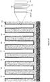
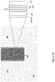
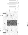
Figures 3A through 3E illustrate respective cross-sectional views of a semiconductor device having a superjunction structure and thediffusion barrier structure 130, during different stages of an embodiment of a manufacturing process. -
Figure 3A shows the semiconductor device after asemiconductor growth substrate 300 such as a Si substrate is provided and afirst epitaxial layer 302 of the first conductivity type is epitaxially grown on thesubstrate 300. Thegrowth substrate 300 may be heavily doped, e.g., to form a drain region of the device. Thefirst epitaxial layer 302 may be doped in situ or ex situ, and forms the drift zone of the device. -
Figure 3B shows the semiconductor device aftertrenches 304 are formed in thefirst epitaxial layer 302. Thetrenches 304 may be etched into thefirst epitaxial layer 302 using any typical trench formation process such as applying a mask / insulating material (not shown) on the frontmain surface 303 of thefirst epitaxial layer 302 and etching thetrenches 304 into thefirst epitaxial layer 302 through respective openings in the mask. -
Figure 3C shows the semiconductor device after the alternating layers ofSi 134 and oxygen-dopedSi 136 of thediffusion barrier structure 130 are epitaxially grown on the sidewalls and bottom of thetrenches 304. According to this embodiment, the alternating layers ofSi 134 and oxygen-dopedSi 136 are epitaxially grown on the sidewalls and the bottom of thetrenches 304 after etching thetrenches 304 into thefirst epitaxial layer 302 but before forming the source and body regions of the device. Thecapping layer 138 of Si may have the same standard in situ doping concentration as the alternating layers ofSi 134 and oxygen-dopedSi 136 and may be doped later with a different dopant species and concentration. Alternatively, thecapping layer 138 of Si may have a different in situ doping concentration compared to the alternating layers ofSi 134 and oxygen-dopedSi 136. -
Figure 3D shows the semiconductor device after thetrenches 304 are filled withepitaxial Si 306 of the second conductivity type. Theepitaxial Si 306 of the second conductivity type may be doped in situ or ex situ and may be planarized, e.g. by chemical-mechanical polishing (CMP). -
Figure 3E shows the semiconductor device after dopant species of the first conductivity type are implanted into a first part of theepitaxial Si 306 of the second conductivity type or into a second Si epitaxial layer grown over theepitaxial Si 306, and after dopant species of the second conductivity type are implanted into a second (deeper) part of theepitaxial Si 306 or second epitaxial layer. The semiconductor device is annealed to activate the implanted dopant species of the first conductivity type to formsource regions 308 of the device, and to activate the implanted dopant species of the second conductivity type to formbody regions 310 of the device. In one embodiment, the annealing is done in a temperature range above 1000 °C for 30 minutes or less. In the case of growing a second epitaxial layer over theepitaxial Si 306 of the second conductivity type, theepitaxial Si 306 of the second conductivity type may be planarized e.g. by CMP before forming the second Si epitaxial layer. -
Gate trenches 312 are also formed in the semiconductor material, and agate electrode 314 is disposed in eachgate trench 312. Thegate electrodes 314 are insulated from the surrounding semiconductor material by agate dielectric 316. Contacttrenches 318 extend through thesource regions 308 and into thebody regions 310. Thecontact trenches 318 are filled with an electrically conductive material 320 such as doped polysilicon, metal, etc. which contacts thesource regions 308 at the sidewall of thecontact trenches 318 and a highly dopedbody contact region 322 at the bottom of thecontact trenches 318. The highly dopedbody contact regions 322 have the same doping type as thebody regions 310, but at a higher concentration to provide good ohmic contact with the electrically conductive material 320 which fills thecontact trenches 318. Aninterlayer dielectric 324 is provided between the electrically conductive material 320 top surface of the semiconductor material. -
Figures 4A through 4O illustrate respective cross-sectional views of a semiconductor device having a superjunction structure and thediffusion barrier structure 130, during different stages of another embodiment of a manufacturing process.Figures 4A through 4O illustrate processing of the semiconductor device in one cell. The semiconductor device may include a plurality of such cells, each cell having the same or similar construction. -
Figure 4A shows the semiconductor device after abase semiconductor material 400 is provided and ahard mask 402 such as a silicon-based hard mask is formed on thebase semiconductor material 400. Thehard mask 402 hasopenings 404 which define the location of trenches to be etched into thebase semiconductor material 400. Thebase semiconductor material 400 may be a growth substrate such as a Si substrate or a Si epitaxial layer grown over such a substrate. -
Figure 4B shows the semiconductor device aftertrenches 406 are etched into thebase semiconductor material 400 and after thediffusion barrier structure 130 is formed along thesidewalls 408 andbottom 410 of thetrenches 406. Thediffusion barrier structure 130 may be formed as previously described herein. -
Figure 4C shows the semiconductor device after a spacer etch process which removes thediffusion barrier structure 130 from the bottom of thetrenches 406. In this case, thebase semiconductor material 400 may form the drift zone of the device and the drift zone may adjoin thebottom 410 of thetrenches 406. Alternatively, the spacer etch process may be skipped so that thediffusion barrier structure 130 remains along the bottom of thetrenches 406. -
Figure 4D shows the semiconductor device after selective epitaxial growth ofsemiconductor material 412 of the second conductivity type in thetrenches 406 and on the top surface of thebase semiconductor material 400. Thesemiconductor material 412 of the second conductivity type which fills thetrenches 406 may be doped in situ or ex situ. In the case of ex situ doping, e.g. if more precise doping dose control is desired, selective epitaxial growth of Si in thetrenches 406 is performed followed by planarization, hard mask removal, masked dopant implantation and dopant activation to defineregions 412 of the second conductivity type in thetrenches 406. In the case of in situ doping, selective epitaxial growth of doped (second conductivity type) Si in thetrenches 406 is performed followed by planarization and hard mask removal. - In the case of in situ or ex situ doping, the
semiconductor material 412 filling thetrenches 406 is planarized, e.g. by CMP which stops on thehard mask 402, and thehard mask 402 is removed, yieldingregions 412 of the second conductivity type which are laterally spaced apart from one another by interveningregions 414 of the drift zone realized by thebase semiconductor material 400. Theregions 412 of the second conductivity type and the interveningregions 414 of the drift zone collectively form a superjunction structure as previously described herein. Onesuch region 412 of the second conductivity type and twosuch intervening regions 414 of the drift zone are shown in the partial cross-sectional view inFigure 4D . In the case of thediffusion barrier structure 130 being removed from the bottom of thetrenches 406 as shown inFigure 4C , the drift zone realized by thebase semiconductor material 400 contacts thebottom face 416 of theregions 412 of the second conductivity type. -
Figure 4E shows the semiconductor device after aSi epitaxial layer 418 of the first conductivity type is grown over thebase semiconductor material 400 of the same conductivity type. TheSi epitaxial layer 418 of the first conductivity type may be doped in situ or ex situ. -
Figure 4F shows the semiconductor device aftergate trenches 420 are etched into theSi epitaxial layer 418 of the first conductivity type, asacrificial oxide 422 is formed on the sidewalls and bottom of thegate trenches 420, and an optional implant of the first conductivity type is performed into the bottom of thegate trenches 420 to form dopedregions 424 of the first conductivity type just below thegate trenches 420. -
Figure 4G shows the semiconductor device after removal of thesacrificial oxide 422 from the sidewalls and bottom of thegate trenches 420, subsequent formation of agate oxide 426 on the sidewalls and bottom of thegate trenches 420, and formation ofgate electrode 428 in thegate trenches 420. Thegate oxide 426 separates thegate electrodes 428 from the surrounding semiconductor material. -
Figure 4H shows the semiconductor device after ascreen oxide 430 is formed on theSi epitaxial layer 418, and after dopant species of the second conductivity type are implanted and driven into alower part 432 of theSi epitaxial layer 418 and dopant species of the first conductivity type are implanted into anupper part 434 of theSi epitaxial layer 418. TheSi epitaxial layer 418 is eventually annealed to activate the implanted dopant species of the first conductivity type to form the source region 434' of each cell and to activate the implanted dopant species of the second conductivity type to form the body region 432' of each cell. In one embodiment, theSi epitaxial layer 418 is annealed in a temperature range above 1000 °C for 30 minutes or less. -
Figure 4I shows the semiconductor device after aninterlayer dielectric 436 is formed on theSi epitaxial layer 418, and after apatterned contact mask 438 such as a photoresist is formed on the interlayer dielectric. Thepatterned contact mask 438 hasopenings 440 aligned with thetrenches 406 formed in thebase semiconductor material 400. -
Figure 4J shows the semiconductor device aftercontact trenches 422 are etched into theSi epitaxial layer 418 and to thesemiconductor material 412 of the second conductivity type which fills thetrenches 406. The contact trench etching process etching exposes asidewall 423 of theSi epitaxial layer 418 and of thebase semiconductor material 400, and may include an anisotropic etch of the exposed part of theinterlayer dielectric 436, an anisotropic etch of the exposed part of theSi epitaxial layer 418, and a lateral etch of theinterlayer dielectric 436 to widen the openings formed in theinterlayer dielectric 436 relative to thetrenches 442 etched into theSi epitaxial layer 418. Thepatterned contact mask 438 is removed after thecontact trenches 442 are formed. -
Figure 4K shows the semiconductor device after deposition of aspacer oxide 444 in thecontact trenches 442. Thespacer oxide 444 is deposited on the exposedsidewall 423 of theSi epitaxial layer 418 and of thebase semiconductor material 400, and on thetop surface 446 of thesemiconductor material 412. -
Figure 4L shows the semiconductor device after removal of thespacer oxide 444 from thetop surface 446 of thesemiconductor material 412 of the second conductivity type which fills thetrenches 406. -
Figure 4M shows the semiconductor device after a recess etch of the exposedtop surface 446 of thesemiconductor material 412 of the second conductivity type which fills thetrenches 406, and after a lateral etch back of the source region 434' to create astep 448 between the source region 434' and the body region 432'. After the lateral etch back, eachcontact trench 422 exposes thesidewall 450 of the adjoining source region 434' and thetop surface 452 of the body region 432'. -
Figure 4N shows the semiconductor device after highly dopedbody contact regions 454 such as p+ regions in the case of an n-channel device are formed in the exposedtop surface 452 of the body region 432' and in the recessed part of thesemiconductor material 412 of the second conductivity type which fills thetrenches 406. The highly dopedbody contact regions 454 provide low ohmic contact to the adjacent semiconductor material. The device may be annealed at this time to activate all previously implanted dopants, including the source and body region dopants. -
Figure 4O shows the semiconductor device after thecontact trenches 442 are filled with an electricallyconductive material 456 which contacts thesidewall 450 of the source region 434' and thetop surface 452 of the body region 432'. In one embodiment, the electricallyconductive material 456 is formed by depositing an electricallyconductive liner 458 such as a Ti or TiN liner in thecontact trenches 442, subsequently filling the contact trenches with ametal 460 such as W, and planarizing themetal 460 e.g. by an etch back process. Ametal layer 462 is then deposited on theinterlayer dielectric 436 using a typical metal lithography process. The metal layer is in contact with the electricallyconductive material 456 which fills thecontact trenches 442. - Spatially relative terms such as "under", "below", "lower", "over", "upper" and the like, are used for ease of description to explain the positioning of one element relative to a second element. These terms are intended to encompass different orientations of the device in addition to different orientations than those depicted in the figures. Further, terms such as "first", "second", and the like, are also used to describe various elements, regions, sections, etc. and are also not intended to be limiting. Like terms refer to like elements throughout the description.
- As used herein, the terms "having", "containing", "including", "comprising" and the like are open-ended terms that indicate the presence of stated elements or features, but do not preclude additional elements or features. The articles "a", "an" and "the" are intended to include the plural as well as the singular, unless the context clearly indicates otherwise.
- With the above range of variations and applications in mind, it should be understood that the present invention is not limited by the foregoing description, nor is it limited by the accompanying drawings. Instead, the present invention is limited only by the following claims and their legal equivalents.
- The invention can be summarized in the following aspects:
- 1st aspect of the invention: A semiconductor device, comprising:
- a source region and a drain region of a first conductivity type;
- a body region of a second conductivity type between the source region and the drain region;
- a gate configured to control current through a channel of the body region;
- a drift zone of the first conductivity type between the body region and the drain region;
- a superjunction structure formed by a plurality of regions of the second conductivity type laterally spaced apart from one another by intervening regions of the drift zone; and
- a diffusion barrier structure disposed along sidewalls of the regions of the second conductivity type, the diffusion barrier structure comprising alternating layers of Si and oxygen-doped Si and a Si capping layer on the alternating layers of Si and oxygen-doped Si.
- 2nd aspect of the invention: The semiconductor device of the 1st aspect, wherein the diffusion barrier structure is also disposed along a bottom face of the regions of the second conductivity type.
- 3rd aspect of the invention: The semiconductor device of the 1st aspect, wherein the drift zone contacts a bottom face of the regions of the second conductivity type.
- 4th aspect of the invention: The semiconductor device of the 1st aspect, wherein the drain region is formed in a Si substrate, wherein the drift zone is disposed in a first Si epitaxial layer formed over the Si substrate, and wherein the source region and the body region are disposed in a second Si epitaxial layer formed over the first Si epitaxial layer.
- 5th aspect of the invention: The semiconductor device of the 4th aspect, wherein the gate is a trench gate formed in the second Si epitaxial layer.
- 6th aspect of the invention: The semiconductor device of the 4th aspect, wherein the gate is a planar gate formed on a surface of the second Si epitaxial layer facing away from the first Si epitaxial layer.
- 7th aspect of the invention: The semiconductor device of the 4th aspect, further comprising a contact in electrical contact with the source region and the body region in the second Si epitaxial layer.
- 8th aspect of the invention: The semiconductor device of the 7th aspect, wherein the contact vertically extends through the second Si epitaxial layer, into the first Si epitaxial layer and electrically contacts a region of the plurality of regions of the second conductivity type, and wherein sidewalls of the contact are laterally separated from the second Si epitaxial layer and the first Si epitaxial layer by an insulating material.
- 9th aspect of the invention: The semiconductor device of the 4th aspect, wherein the second Si epitaxial layer contacts a top face of the regions of the second conductivity type.
- 10th aspect of the invention: A method of manufacturing a semiconductor device, the method comprising:
- forming a source region and a drain region of a first conductivity type;
- forming a body region of a second conductivity type, wherein the body region is disposed between the source region and the drain region;
- forming a gate configured to control current through a channel of the body region;
- forming a drift zone of the first conductivity type, wherein the drift zone is disposed between the body region and the drain region;
- forming a plurality of regions of the second conductivity type laterally spaced apart from one another by intervening regions of the drift zone, to form a superjunction structure; and
- forming a diffusion barrier structure along sidewalls of the regions of the second conductivity type of the superjunction structure, the diffusion barrier structure comprising alternating layers of Si and oxygen-doped Si and a Si capping layer on the alternating layers of Si and oxygen-doped Si.
- 11th aspect of the invention: The method of the 10th aspect, wherein forming the plurality of regions of the second conductivity type and forming the diffusion barrier structure along sidewalls of the regions of the second conductivity type comprises:
- etching a plurality of trenches in a first Si epitaxial layer of the first conductivity type, wherein the first Si epitaxial layer includes the drift zone;
- epitaxially growing the alternating layers of Si and oxygen-doped Si on sidewalls and a bottom of the trenches;
- epitaxially growing the Si capping layer on the alternating layers of Si and oxygen-doped Si; and
- after forming the diffusion barrier structure, filling the trenches with epitaxial Si of the second conductivity type.
- 12th aspect of the invention: The method of the 11th aspect, wherein forming the source region and the body region comprises:
- after filling the trenches with the epitaxial Si of the second conductivity type, forming a second Si epitaxial layer over the first Si epitaxial layer;
- implanting dopant species of the first conductivity type into a first part of the second Si epitaxial layer which corresponds to the source region;
- implanting dopant species of the second conductivity type into a second part of the second Si epitaxial layer which corresponds to the body region; and
- annealing the second Si epitaxial layer to activate the implanted dopant species of the first conductivity type to form the source region and to activate the implanted dopant species of the second conductivity type to form the body region.
- 13th aspect of the invention: The method of the 12th aspect, wherein the drain region is disposed in a Si substrate over which the first Si epitaxial layer is formed.
- 14th aspect of the invention: The method of the 12th aspect, wherein the second Si epitaxial layer is annealed in a temperature range above 1000 °C for 30 minutes or less.
- 15th aspect of the invention: The method of the 12th aspect, further comprising:
planarizing the epitaxial Si of the second conductivity type before forming the second Si epitaxial layer. - 16th aspect of the invention: The method of the 12th aspect, further comprising:
- etching a contact trench into the second Si epitaxial layer, the contact trench exposing a sidewall of the source region and a top surface of the body region; and
- filling the contact trench with an electrically conductive material which contacts the sidewall of the source region and the top surface of the body region.
- 17th aspect of the invention: The method of the 16th aspect, wherein etching the contact trench further comprises:
- etching the contact trench into the first Si epitaxial layer to expose a sidewall of the first Si epitaxial layer;
- depositing an insulating material on the sidewall of the body region and the sidewall of the first Si epitaxial layer; and
- etching the contact trench into a region of the plurality of regions of the second conductivity type,
- wherein the electrically conductive material is in contact with the region of the second conductivity type into which the contact trench is etched,
- wherein sidewalls of the electrically conductive material are laterally separated from the second Si epitaxial layer and the first Si epitaxial layer by the insulating material.
- 18th aspect of the invention: The method of the 11th aspect, further comprising:
removing the alternating layers of Si and oxygen-doped Si and the Si capping layer from the bottom of the plurality of trenches before filling the plurality of trenches with the epitaxial Si of the second conductivity type, so that the bottom of the plurality of trenches is uncovered when the plurality of trenches is filled with the epitaxial Si of the second conductivity type. - 19th aspect of the invention: The method of the 11th aspect, wherein filling the plurality of trenches with the epitaxial Si of the second conductivity type comprises:
- selectively growing in situ doped epitaxial Si of the second conductivity type in the plurality of trenches; and
- planarizing the in situ doped epitaxial Si of the second conductivity type before forming the second Si epitaxial layer.
- 20th aspect of the invention: The method of the 11th aspect, wherein filling the plurality of trenches with the epitaxial Si of the second conductivity type comprises:
- selectively growing epitaxial Si in the plurality of trenches;
- planarizing the epitaxial Si;
- implanting dopant species of the second conductivity type into the planarized epitaxial Si; and
- annealing the first Si epitaxial layer to activate the implanted dopant species of the second conductivity type.
Claims (15)
- A semiconductor device (100), comprising:a source region (102) and a drain region (104) of a first conductivity type;a body region (106) of a second conductivity type between the source region (102) and the drain region (104);a gate (108) configured to control current through a channel (114) of the body region (106);a drift zone (116) of the first conductivity type between the body region (106) and the drain region (104);a superjunction structure formed by a plurality of regions (118) of the second conductivity type laterally spaced apart from one another by intervening regions (120) of the drift zone (116); anda diffusion barrier structure (130) disposed along sidewalls (132) of the regions (118) of the second conductivity type, the diffusion barrier structure (130) comprising alternating layers of Si (134) and oxygen-doped Si (136) and a Si capping layer (138) on the alternating layers of Si (134) and oxygen-doped Si (136).
- The semiconductor device (100) of claim 1, wherein the diffusion barrier structure (130) is also disposed along a bottom face (133) of the regions (118) of the second conductivity type.
- The semiconductor device (100) of claim 1, wherein the drift zone (116) contacts a bottom face (133) of the regions (118) of the second conductivity type.
- The semiconductor device (100) of any of the preceding claims, wherein the drain region (104) is formed in a Si substrate, wherein the drift zone (116) is disposed in a first Si epitaxial layer (302) formed over the Si substrate, and wherein the source region (102) and the body region (106) are disposed in a second Si epitaxial layer formed over the first Si epitaxial layer (302), the second Si epitaxial layer preferably contacting a top face of the regions (118) of the second conductivity type.
- The semiconductor device (100) of claim 4, wherein the gate is a trench gate (202) formed in the second Si epitaxial layer.
- The semiconductor device (100) of claim 4, wherein the gate is a planar gate (108) formed on a surface of the second Si epitaxial layer facing away from the first Si epitaxial layer (302).
- The semiconductor device (100) of any of claims 4 to 6, further comprising a contact in electrical contact with the source region (102) and the body region (106) in the second Si epitaxial layer,
wherein the contact preferably extends through the second Si epitaxial layer vertically, into the first Si epitaxial layer (302) and electrically contacts a region of the plurality of regions (118) of the second conductivity type, and wherein sidewalls (132) of the contact are laterally separated from the second Si epitaxial layer and the first Si epitaxial layer (302) by an insulating material. - A method of manufacturing a semiconductor device (100), preferably the semiconductor device (100) of any of the preceding claims, the method comprising:forming a source region (102) and a drain region (104) of a first conductivity type;forming a body region (106) of a second conductivity type, wherein the body region (106) is disposed between the source region (102) and the drain region (104);forming a gate (108) configured to control current through a channel (114) of the body region (106);forming a drift zone (116) of the first conductivity type, wherein the drift zone (116) is disposed between the body region (106) and the drain region (104);forming a plurality of regions (118) of the second conductivity type laterally spaced apart from one another by intervening regions (120) of the drift zone (116), to form a superjunction structure; andforming a diffusion barrier structure (130) along sidewalls (132) of the regions (118) of the second conductivity type of the superjunction structure, the diffusion barrier structure (130) comprising alternating layers of Si (134) and oxygen-doped Si (136) and a Si capping layer (138) on the alternating layers of Si (134) and oxygen-doped Si (136).
- The method of claim 8, wherein forming the plurality of regions (118) of the second conductivity type and forming the diffusion barrier structure (130) along sidewalls (132) of the regions (118) of the second conductivity type comprises:etching a plurality of trenches in a first Si epitaxial layer (302) of the first conductivity type, which includes the drift zone (116), the first Si epitaxial being preferably formed over a Si substrate in which the drain region (104) is disposed;epitaxially growing the alternating layers of Si (134) and oxygen-doped Si (136) on sidewalls (132) and a bottom of the trenches;epitaxially growing the Si capping layer (138) on the alternating layers of Si (134) and oxygen-doped Si (136); andafter forming the diffusion barrier structure (130), filling the trenches with epitaxial Si of the second conductivity type.
- The method of claim 9, wherein forming the source region (102) and the body region (106) comprises:after filling the trenches with the epitaxial Si of the second conductivity type, forming a second Si epitaxial layer over the first Si epitaxial layer (302), preferably after planarizing the epitaxial Si of the second conductivity type;implanting dopant species of the first conductivity type into a first part of the second Si epitaxial layer which corresponds to the source region (102);implanting dopant species of the second conductivity type into a second part of the second Si epitaxial layer which corresponds to the body region (106); andannealing the second Si epitaxial layer, preferably in a temperature range above 1000 °C for 30 minutes or less, to activate the implanted dopant species of the first conductivity type to form the source region (102) and to activate the implanted dopant species of the second conductivity type to form the body region (106).
- The method of claim 10, further comprising:etching a contact trench into the second Si epitaxial layer, the contact trench exposing a sidewall of the source region (102) and a top surface of the body region (106); andfilling the contact trench with an electrically conductive material which contacts the sidewall of the source region (102) and the top surface of the body region (106).
- The method of claim 11, wherein etching the contact trench further comprises:etching the contact trench into the first Si epitaxial layer (302) to expose a sidewall of the first Si epitaxial layer (302);depositing an insulating material on the sidewall of the body region (106) and the sidewall of the first Si epitaxial layer (302); andetching the contact trench into a region of the plurality of regions (118) of the second conductivity type,wherein the electrically conductive material is in contact with the region of the second conductivity type into which the contact trench is etched,wherein sidewalls (132) of the electrically conductive material are laterally separated from the second Si epitaxial layer and the first Si epitaxial layer (302) by the insulating material.
- The method of any of claims 9-12, further comprising:
removing the alternating layers of Si (134) and oxygen-doped Si (136) and the Si capping layer (138) from the bottom of the plurality of trenches before filling the plurality of trenches with the epitaxial Si of the second conductivity type, so that the bottom of the plurality of trenches is uncovered when the plurality of trenches is filled with the epitaxial Si of the second conductivity type. - The method of any of claims 9-13, wherein filling the plurality of trenches with the epitaxial Si of the second conductivity type comprises:selectively growing in situ doped epitaxial Si of the second conductivity type in the plurality of trenches; andplanarizing the in situ doped epitaxial Si of the second conductivity type before forming the second Si epitaxial layer.
- The method of any of claims 9-13, wherein filling the plurality of trenches with the epitaxial Si of the second conductivity type comprises:selectively growing epitaxial Si in the plurality of trenches;planarizing the epitaxial Si;implanting dopant species of the second conductivity type into the planarized epitaxial Si; andannealing the first Si epitaxial layer (302) to activate the implanted dopant species of the second conductivity type.
Applications Claiming Priority (1)
| Application Number | Priority Date | Filing Date | Title |
|---|---|---|---|
| US16/185,610 US10790353B2 (en) | 2018-11-09 | 2018-11-09 | Semiconductor device with superjunction and oxygen inserted Si-layers |
Publications (2)
| Publication Number | Publication Date |
|---|---|
| EP3651202A1 true EP3651202A1 (en) | 2020-05-13 |
| EP3651202B1 EP3651202B1 (en) | 2022-07-06 |
Family
ID=68424824
Family Applications (1)
| Application Number | Title | Priority Date | Filing Date |
|---|---|---|---|
| EP19206536.5A Active EP3651202B1 (en) | 2018-11-09 | 2019-10-31 | Semiconductor device with superjunction and oxygen inserted si-layers |
Country Status (4)
| Country | Link |
|---|---|
| US (2) | US10790353B2 (en) |
| EP (1) | EP3651202B1 (en) |
| KR (1) | KR20200054881A (en) |
| CN (1) | CN111180522B (en) |
Cited By (3)
| Publication number | Priority date | Publication date | Assignee | Title |
|---|---|---|---|---|
| CN112670335A (en) * | 2020-12-30 | 2021-04-16 | 无锡紫光微电子有限公司 | Super-junction shielding gate structure IGBT manufactured through multiple times of epitaxy and manufacturing method |
| CN112820645A (en) * | 2020-12-31 | 2021-05-18 | 北京燕东微电子科技有限公司 | Power semiconductor device and preparation method thereof |
| CN113871481A (en) * | 2020-10-19 | 2021-12-31 | 南京江智科技有限公司 | A semiconductor power device with a silicon carbide superjunction |
Families Citing this family (8)
| Publication number | Priority date | Publication date | Assignee | Title |
|---|---|---|---|---|
| US10790353B2 (en) | 2018-11-09 | 2020-09-29 | Infineon Technologies Austria Ag | Semiconductor device with superjunction and oxygen inserted Si-layers |
| US11804531B2 (en) * | 2020-07-23 | 2023-10-31 | Taiwan Semiconductor Manufacturing Co., Ltd. | Thin film transfer using substrate with etch stop layer and diffusion barrier layer |
| CN113488523A (en) * | 2021-06-07 | 2021-10-08 | 西安电子科技大学 | High-voltage MOSFET device with super-junction double-channel gate and preparation method thereof |
| US11908904B2 (en) * | 2021-08-12 | 2024-02-20 | Infineon Technologies Austria Ag | Planar gate semiconductor device with oxygen-doped Si-layers |
| EP4627895A1 (en) * | 2023-08-23 | 2025-10-08 | Scdevice LLC | Vertical semiconductor devices with deep well region for radiation hardening |
| US20260068242A1 (en) * | 2024-08-29 | 2026-03-05 | Applied Materials, Inc. | Wide-bandgap super junction structures for power devices |
| US20260068241A1 (en) * | 2024-08-29 | 2026-03-05 | Applied Materials, Inc. | Epi liner super junction devices with diffusion barrier |
| CN122002828B (en) * | 2026-02-12 | 2026-07-31 | 上海华虹挚芯电子科技有限公司 | Small-size CT (computed tomography) open-pore groove type IGBT device and manufacturing method thereof |
Citations (4)
| Publication number | Priority date | Publication date | Assignee | Title |
|---|---|---|---|---|
| US20070249142A1 (en) * | 2006-04-19 | 2007-10-25 | Toyota Jidosha Kabushiki Kaisha | Semiconductor devices and method of manufacturing them |
| DE102007044414A1 (en) * | 2007-09-17 | 2009-03-19 | Infineon Technologies Austria Ag | Semiconductor component e.g. MOS field effect transistor, has intermediate zones arranged on ditch walls, where intermediate zones are high-impedance with respect to loading compensation zones and drift zones |
| WO2009079465A1 (en) * | 2007-12-14 | 2009-06-25 | Fairchild Semiconductor Corporation | Structure and method for forming power devices with high aspect ratio contact openings |
| US20130313632A1 (en) * | 2011-06-30 | 2013-11-28 | Infineon Technologies Austria Ag | Semiconductor Device with Voltage Compensation Structure |
Family Cites Families (29)
| Publication number | Priority date | Publication date | Assignee | Title |
|---|---|---|---|---|
| US6404007B1 (en) * | 1999-04-05 | 2002-06-11 | Fairchild Semiconductor Corporation | Trench transistor with superior gate dielectric |
| US7345342B2 (en) | 2001-01-30 | 2008-03-18 | Fairchild Semiconductor Corporation | Power semiconductor devices and methods of manufacture |
| US7009247B2 (en) * | 2001-07-03 | 2006-03-07 | Siliconix Incorporated | Trench MIS device with thick oxide layer in bottom of gate contact trench |
| US6639276B2 (en) * | 2001-07-05 | 2003-10-28 | International Rectifier Corporation | Power MOSFET with ultra-deep base and reduced on resistance |
| US6566201B1 (en) * | 2001-12-31 | 2003-05-20 | General Semiconductor, Inc. | Method for fabricating a high voltage power MOSFET having a voltage sustaining region that includes doped columns formed by rapid diffusion |
| TWI248136B (en) * | 2002-03-19 | 2006-01-21 | Infineon Technologies Ag | Method for fabricating a transistor arrangement having trench transistor cells having a field electrode |
| DE102006002903A1 (en) | 2006-01-20 | 2007-08-02 | Infineon Technologies Austria Ag | Treatment of oxygen-containing semiconductor wafer, comprises irradiating second side of wafer with high-energy particles to produce crystal defects in second semiconductor region of wafer, and heating wafer |
| US7541260B2 (en) * | 2007-02-21 | 2009-06-02 | Infineon Technologies Austria Ag | Trench diffusion isolation in semiconductor devices |
| US20090053869A1 (en) | 2007-08-22 | 2009-02-26 | Infineon Technologies Austria Ag | Method for producing an integrated circuit including a trench transistor and integrated circuit |
| US7867852B2 (en) * | 2008-08-08 | 2011-01-11 | Alpha And Omega Semiconductor Incorporated | Super-self-aligned trench-dmos structure and method |
| US8253194B2 (en) | 2008-09-17 | 2012-08-28 | Fairchild Semiconductor Corporation | Structures for reducing dopant out-diffusion from implant regions in power devices |
| JP2010103260A (en) * | 2008-10-22 | 2010-05-06 | Toshiba Corp | Method of manufacturing semiconductor device for power control |
| US8648413B2 (en) * | 2009-12-28 | 2014-02-11 | Force Mos Technology Co., Ltd. | Super-junction trench MOSFET with multiple trenched source-body contacts |
| US8372717B2 (en) * | 2009-12-28 | 2013-02-12 | Force Mos Technology Co., Ltd. | Method for manufacturing a super-junction trench MOSFET with resurf stepped oxides and trenched contacts |
| US8067800B2 (en) | 2009-12-28 | 2011-11-29 | Force Mos Technology Co., Ltd. | Super-junction trench MOSFET with resurf step oxide and the method to make the same |
| US8373225B2 (en) * | 2009-12-28 | 2013-02-12 | Force Mos Technology Co., Ltd. | Super-junction trench MOSFET with Resurf stepped oxides and split gate electrodes |
| US8373224B2 (en) * | 2009-12-28 | 2013-02-12 | Force Mos Technology Co., Ltd. | Super-junction trench MOSFET with resurf stepped oxides and trenched contacts |
| US8587054B2 (en) * | 2011-12-30 | 2013-11-19 | Force Mos Technology Co., Ltd. | Trench MOSFET with resurf stepped oxide and diffused drift region |
| US8975662B2 (en) * | 2012-06-14 | 2015-03-10 | Infineon Technologies Austria Ag | Method of manufacturing a semiconductor device using an impurity source containing a metallic recombination element and semiconductor device |
| JP6226786B2 (en) | 2014-03-19 | 2017-11-08 | 三菱電機株式会社 | Semiconductor device and manufacturing method thereof |
| KR102335772B1 (en) | 2015-04-07 | 2021-12-06 | 삼성전자주식회사 | Electronic devices having side gate and 2D material channel and method of manufacturing the same |
| DE102016104327B4 (en) | 2016-03-09 | 2023-12-28 | Infineon Technologies Austria Ag | Method of manufacturing a semiconductor device |
| CN107768371A (en) * | 2017-10-24 | 2018-03-06 | 贵州芯长征科技有限公司 | Super node MOSFET structure of integrated schottky knot and preparation method thereof |
| US10741638B2 (en) | 2018-08-08 | 2020-08-11 | Infineon Technologies Austria Ag | Oxygen inserted Si-layers for reduced substrate dopant outdiffusion in power devices |
| US10580888B1 (en) | 2018-08-08 | 2020-03-03 | Infineon Technologies Austria Ag | Oxygen inserted Si-layers for reduced contact implant outdiffusion in vertical power devices |
| US10573742B1 (en) | 2018-08-08 | 2020-02-25 | Infineon Technologies Austria Ag | Oxygen inserted Si-layers in vertical trench power devices |
| US10510836B1 (en) | 2018-08-08 | 2019-12-17 | Infineon Technologies Austria Ag | Gate trench device with oxygen inserted si-layers |
| US10790353B2 (en) | 2018-11-09 | 2020-09-29 | Infineon Technologies Austria Ag | Semiconductor device with superjunction and oxygen inserted Si-layers |
| EP3761371B1 (en) | 2019-07-04 | 2025-06-25 | Infineon Technologies Austria AG | Semiconductor transistor device and method of manufacturing the same |
-
2018
- 2018-11-09 US US16/185,610 patent/US10790353B2/en active Active
-
2019
- 2019-10-31 EP EP19206536.5A patent/EP3651202B1/en active Active
- 2019-11-07 KR KR1020190141617A patent/KR20200054881A/en not_active Withdrawn
- 2019-11-08 CN CN201911087459.9A patent/CN111180522B/en active Active
-
2020
- 2020-07-16 US US16/930,500 patent/US11545545B2/en active Active
Patent Citations (4)
| Publication number | Priority date | Publication date | Assignee | Title |
|---|---|---|---|---|
| US20070249142A1 (en) * | 2006-04-19 | 2007-10-25 | Toyota Jidosha Kabushiki Kaisha | Semiconductor devices and method of manufacturing them |
| DE102007044414A1 (en) * | 2007-09-17 | 2009-03-19 | Infineon Technologies Austria Ag | Semiconductor component e.g. MOS field effect transistor, has intermediate zones arranged on ditch walls, where intermediate zones are high-impedance with respect to loading compensation zones and drift zones |
| WO2009079465A1 (en) * | 2007-12-14 | 2009-06-25 | Fairchild Semiconductor Corporation | Structure and method for forming power devices with high aspect ratio contact openings |
| US20130313632A1 (en) * | 2011-06-30 | 2013-11-28 | Infineon Technologies Austria Ag | Semiconductor Device with Voltage Compensation Structure |
Cited By (5)
| Publication number | Priority date | Publication date | Assignee | Title |
|---|---|---|---|---|
| CN113871481A (en) * | 2020-10-19 | 2021-12-31 | 南京江智科技有限公司 | A semiconductor power device with a silicon carbide superjunction |
| CN113871481B (en) * | 2020-10-19 | 2023-07-25 | 南京江智科技有限公司 | Semiconductor power device with silicon carbide super junction |
| CN112670335A (en) * | 2020-12-30 | 2021-04-16 | 无锡紫光微电子有限公司 | Super-junction shielding gate structure IGBT manufactured through multiple times of epitaxy and manufacturing method |
| CN112820645A (en) * | 2020-12-31 | 2021-05-18 | 北京燕东微电子科技有限公司 | Power semiconductor device and preparation method thereof |
| CN112820645B (en) * | 2020-12-31 | 2022-07-05 | 北京燕东微电子科技有限公司 | Power semiconductor device and preparation method thereof |
Also Published As
| Publication number | Publication date |
|---|---|
| US10790353B2 (en) | 2020-09-29 |
| US20200350401A1 (en) | 2020-11-05 |
| CN111180522A (en) | 2020-05-19 |
| US20200152733A1 (en) | 2020-05-14 |
| KR20200054881A (en) | 2020-05-20 |
| US11545545B2 (en) | 2023-01-03 |
| EP3651202B1 (en) | 2022-07-06 |
| CN111180522B (en) | 2024-10-18 |
Similar Documents
| Publication | Publication Date | Title |
|---|---|---|
| US11545545B2 (en) | Superjunction device with oxygen inserted Si-layers | |
| CN111727491B (en) | Structure and method for self-aligned trench MOSFET | |
| JP4088033B2 (en) | Semiconductor device | |
| US8373208B2 (en) | Lateral super junction device with high substrate-gate breakdown and built-in avalanche clamp diode | |
| US7393749B2 (en) | Charge balance field effect transistor | |
| US8969953B2 (en) | Method of forming a self-aligned charge balanced power DMOS | |
| US7700440B2 (en) | Method of manufacturing a metal-oxide-semiconductor with reduced on-resistance | |
| US11594613B2 (en) | Sawtooh electric field drift region structure for planar and trench power semiconductor devices | |
| US8304312B2 (en) | Charged balanced devices with shielded gate trench | |
| US8860130B2 (en) | Charged balanced devices with shielded gate trench | |
| US9000516B2 (en) | Super-junction device and method of forming the same | |
| US6846706B2 (en) | Power MOSFET with ultra-deep base and reduced on resistance | |
| US9356134B2 (en) | Charged balanced devices with shielded gate trench | |
| US20190122926A1 (en) | Self-Aligned Shielded Trench MOSFETs and Related Fabrication Methods | |
| EP3608969B1 (en) | Oxygen inserted si-layers for reduced substrate dopant outdiffusion in power devices | |
| WO2010098742A1 (en) | Trench device structure and fabrication |
Legal Events
| Date | Code | Title | Description |
|---|---|---|---|
| PUAI | Public reference made under article 153(3) epc to a published international application that has entered the european phase |
Free format text: ORIGINAL CODE: 0009012 |
|
| STAA | Information on the status of an ep patent application or granted ep patent |
Free format text: STATUS: THE APPLICATION HAS BEEN PUBLISHED |
|
| AK | Designated contracting states |
Kind code of ref document: A1 Designated state(s): AL AT BE BG CH CY CZ DE DK EE ES FI FR GB GR HR HU IE IS IT LI LT LU LV MC MK MT NL NO PL PT RO RS SE SI SK SM TR |
|
| AX | Request for extension of the european patent |
Extension state: BA ME |
|
| STAA | Information on the status of an ep patent application or granted ep patent |
Free format text: STATUS: REQUEST FOR EXAMINATION WAS MADE |
|
| 17P | Request for examination filed |
Effective date: 20200929 |
|
| RBV | Designated contracting states (corrected) |
Designated state(s): AL AT BE BG CH CY CZ DE DK EE ES FI FR GB GR HR HU IE IS IT LI LT LU LV MC MK MT NL NO PL PT RO RS SE SI SK SM TR |
|
| GRAP | Despatch of communication of intention to grant a patent |
Free format text: ORIGINAL CODE: EPIDOSNIGR1 |
|
| STAA | Information on the status of an ep patent application or granted ep patent |
Free format text: STATUS: GRANT OF PATENT IS INTENDED |
|
| INTG | Intention to grant announced |
Effective date: 20220207 |
|
| GRAS | Grant fee paid |
Free format text: ORIGINAL CODE: EPIDOSNIGR3 |
|
| GRAA | (expected) grant |
Free format text: ORIGINAL CODE: 0009210 |
|
| STAA | Information on the status of an ep patent application or granted ep patent |
Free format text: STATUS: THE PATENT HAS BEEN GRANTED |
|
| AK | Designated contracting states |
Kind code of ref document: B1 Designated state(s): AL AT BE BG CH CY CZ DE DK EE ES FI FR GB GR HR HU IE IS IT LI LT LU LV MC MK MT NL NO PL PT RO RS SE SI SK SM TR |
|
| REG | Reference to a national code |
Ref country code: AT Ref legal event code: REF Ref document number: 1503483 Country of ref document: AT Kind code of ref document: T Effective date: 20220715 Ref country code: CH Ref legal event code: EP |
|
| REG | Reference to a national code |
Ref country code: DE Ref legal event code: R096 Ref document number: 602019016642 Country of ref document: DE |
|
| REG | Reference to a national code |
Ref country code: IE Ref legal event code: FG4D |
|
| REG | Reference to a national code |
Ref country code: LT Ref legal event code: MG9D |
|
| REG | Reference to a national code |
Ref country code: NL Ref legal event code: MP Effective date: 20220706 |
|
| PG25 | Lapsed in a contracting state [announced via postgrant information from national office to epo] |
Ref country code: SE Free format text: LAPSE BECAUSE OF FAILURE TO SUBMIT A TRANSLATION OF THE DESCRIPTION OR TO PAY THE FEE WITHIN THE PRESCRIBED TIME-LIMIT Effective date: 20220706 Ref country code: RS Free format text: LAPSE BECAUSE OF FAILURE TO SUBMIT A TRANSLATION OF THE DESCRIPTION OR TO PAY THE FEE WITHIN THE PRESCRIBED TIME-LIMIT Effective date: 20220706 Ref country code: PT Free format text: LAPSE BECAUSE OF FAILURE TO SUBMIT A TRANSLATION OF THE DESCRIPTION OR TO PAY THE FEE WITHIN THE PRESCRIBED TIME-LIMIT Effective date: 20221107 Ref country code: NO Free format text: LAPSE BECAUSE OF FAILURE TO SUBMIT A TRANSLATION OF THE DESCRIPTION OR TO PAY THE FEE WITHIN THE PRESCRIBED TIME-LIMIT Effective date: 20221006 Ref country code: NL Free format text: LAPSE BECAUSE OF FAILURE TO SUBMIT A TRANSLATION OF THE DESCRIPTION OR TO PAY THE FEE WITHIN THE PRESCRIBED TIME-LIMIT Effective date: 20220706 Ref country code: LV Free format text: LAPSE BECAUSE OF FAILURE TO SUBMIT A TRANSLATION OF THE DESCRIPTION OR TO PAY THE FEE WITHIN THE PRESCRIBED TIME-LIMIT Effective date: 20220706 Ref country code: LT Free format text: LAPSE BECAUSE OF FAILURE TO SUBMIT A TRANSLATION OF THE DESCRIPTION OR TO PAY THE FEE WITHIN THE PRESCRIBED TIME-LIMIT Effective date: 20220706 Ref country code: FI Free format text: LAPSE BECAUSE OF FAILURE TO SUBMIT A TRANSLATION OF THE DESCRIPTION OR TO PAY THE FEE WITHIN THE PRESCRIBED TIME-LIMIT Effective date: 20220706 Ref country code: ES Free format text: LAPSE BECAUSE OF FAILURE TO SUBMIT A TRANSLATION OF THE DESCRIPTION OR TO PAY THE FEE WITHIN THE PRESCRIBED TIME-LIMIT Effective date: 20220706 |
|
| REG | Reference to a national code |
Ref country code: AT Ref legal event code: MK05 Ref document number: 1503483 Country of ref document: AT Kind code of ref document: T Effective date: 20220706 |
|
| PG25 | Lapsed in a contracting state [announced via postgrant information from national office to epo] |
Ref country code: PL Free format text: LAPSE BECAUSE OF FAILURE TO SUBMIT A TRANSLATION OF THE DESCRIPTION OR TO PAY THE FEE WITHIN THE PRESCRIBED TIME-LIMIT Effective date: 20220706 Ref country code: IS Free format text: LAPSE BECAUSE OF FAILURE TO SUBMIT A TRANSLATION OF THE DESCRIPTION OR TO PAY THE FEE WITHIN THE PRESCRIBED TIME-LIMIT Effective date: 20221106 Ref country code: HR Free format text: LAPSE BECAUSE OF FAILURE TO SUBMIT A TRANSLATION OF THE DESCRIPTION OR TO PAY THE FEE WITHIN THE PRESCRIBED TIME-LIMIT Effective date: 20220706 Ref country code: GR Free format text: LAPSE BECAUSE OF FAILURE TO SUBMIT A TRANSLATION OF THE DESCRIPTION OR TO PAY THE FEE WITHIN THE PRESCRIBED TIME-LIMIT Effective date: 20221007 |
|
| REG | Reference to a national code |
Ref country code: DE Ref legal event code: R097 Ref document number: 602019016642 Country of ref document: DE |
|
| PG25 | Lapsed in a contracting state [announced via postgrant information from national office to epo] |
Ref country code: SM Free format text: LAPSE BECAUSE OF FAILURE TO SUBMIT A TRANSLATION OF THE DESCRIPTION OR TO PAY THE FEE WITHIN THE PRESCRIBED TIME-LIMIT Effective date: 20220706 Ref country code: RO Free format text: LAPSE BECAUSE OF FAILURE TO SUBMIT A TRANSLATION OF THE DESCRIPTION OR TO PAY THE FEE WITHIN THE PRESCRIBED TIME-LIMIT Effective date: 20220706 Ref country code: DK Free format text: LAPSE BECAUSE OF FAILURE TO SUBMIT A TRANSLATION OF THE DESCRIPTION OR TO PAY THE FEE WITHIN THE PRESCRIBED TIME-LIMIT Effective date: 20220706 Ref country code: CZ Free format text: LAPSE BECAUSE OF FAILURE TO SUBMIT A TRANSLATION OF THE DESCRIPTION OR TO PAY THE FEE WITHIN THE PRESCRIBED TIME-LIMIT Effective date: 20220706 Ref country code: AT Free format text: LAPSE BECAUSE OF FAILURE TO SUBMIT A TRANSLATION OF THE DESCRIPTION OR TO PAY THE FEE WITHIN THE PRESCRIBED TIME-LIMIT Effective date: 20220706 |
|
| PLBE | No opposition filed within time limit |
Free format text: ORIGINAL CODE: 0009261 |
|
| STAA | Information on the status of an ep patent application or granted ep patent |
Free format text: STATUS: NO OPPOSITION FILED WITHIN TIME LIMIT |
|
| PG25 | Lapsed in a contracting state [announced via postgrant information from national office to epo] |
Ref country code: SK Free format text: LAPSE BECAUSE OF FAILURE TO SUBMIT A TRANSLATION OF THE DESCRIPTION OR TO PAY THE FEE WITHIN THE PRESCRIBED TIME-LIMIT Effective date: 20220706 Ref country code: MC Free format text: LAPSE BECAUSE OF FAILURE TO SUBMIT A TRANSLATION OF THE DESCRIPTION OR TO PAY THE FEE WITHIN THE PRESCRIBED TIME-LIMIT Effective date: 20220706 Ref country code: EE Free format text: LAPSE BECAUSE OF FAILURE TO SUBMIT A TRANSLATION OF THE DESCRIPTION OR TO PAY THE FEE WITHIN THE PRESCRIBED TIME-LIMIT Effective date: 20220706 |
|
| REG | Reference to a national code |
Ref country code: CH Ref legal event code: PL |
|
| 26N | No opposition filed |
Effective date: 20230411 |
|
| REG | Reference to a national code |
Ref country code: BE Ref legal event code: MM Effective date: 20221031 |
|
| PG25 | Lapsed in a contracting state [announced via postgrant information from national office to epo] |
Ref country code: LU Free format text: LAPSE BECAUSE OF NON-PAYMENT OF DUE FEES Effective date: 20221031 Ref country code: AL Free format text: LAPSE BECAUSE OF FAILURE TO SUBMIT A TRANSLATION OF THE DESCRIPTION OR TO PAY THE FEE WITHIN THE PRESCRIBED TIME-LIMIT Effective date: 20220706 |
|
| P01 | Opt-out of the competence of the unified patent court (upc) registered |
Effective date: 20230528 |
|
| PG25 | Lapsed in a contracting state [announced via postgrant information from national office to epo] |
Ref country code: LI Free format text: LAPSE BECAUSE OF NON-PAYMENT OF DUE FEES Effective date: 20221031 Ref country code: FR Free format text: LAPSE BECAUSE OF NON-PAYMENT OF DUE FEES Effective date: 20221031 Ref country code: CH Free format text: LAPSE BECAUSE OF NON-PAYMENT OF DUE FEES Effective date: 20221031 |
|
| PG25 | Lapsed in a contracting state [announced via postgrant information from national office to epo] |
Ref country code: SI Free format text: LAPSE BECAUSE OF FAILURE TO SUBMIT A TRANSLATION OF THE DESCRIPTION OR TO PAY THE FEE WITHIN THE PRESCRIBED TIME-LIMIT Effective date: 20220706 |
|
| PG25 | Lapsed in a contracting state [announced via postgrant information from national office to epo] |
Ref country code: BE Free format text: LAPSE BECAUSE OF NON-PAYMENT OF DUE FEES Effective date: 20221031 |
|
| PG25 | Lapsed in a contracting state [announced via postgrant information from national office to epo] |
Ref country code: IE Free format text: LAPSE BECAUSE OF NON-PAYMENT OF DUE FEES Effective date: 20221031 |
|
| PG25 | Lapsed in a contracting state [announced via postgrant information from national office to epo] |
Ref country code: IT Free format text: LAPSE BECAUSE OF FAILURE TO SUBMIT A TRANSLATION OF THE DESCRIPTION OR TO PAY THE FEE WITHIN THE PRESCRIBED TIME-LIMIT Effective date: 20220706 |
|
| PG25 | Lapsed in a contracting state [announced via postgrant information from national office to epo] |
Ref country code: HU Free format text: LAPSE BECAUSE OF FAILURE TO SUBMIT A TRANSLATION OF THE DESCRIPTION OR TO PAY THE FEE WITHIN THE PRESCRIBED TIME-LIMIT; INVALID AB INITIO Effective date: 20191031 |
|
| PG25 | Lapsed in a contracting state [announced via postgrant information from national office to epo] |
Ref country code: CY Free format text: LAPSE BECAUSE OF FAILURE TO SUBMIT A TRANSLATION OF THE DESCRIPTION OR TO PAY THE FEE WITHIN THE PRESCRIBED TIME-LIMIT Effective date: 20220706 |
|
| PG25 | Lapsed in a contracting state [announced via postgrant information from national office to epo] |
Ref country code: MK Free format text: LAPSE BECAUSE OF FAILURE TO SUBMIT A TRANSLATION OF THE DESCRIPTION OR TO PAY THE FEE WITHIN THE PRESCRIBED TIME-LIMIT Effective date: 20220706 |
|
| GBPC | Gb: european patent ceased through non-payment of renewal fee |
Effective date: 20231031 |
|
| PG25 | Lapsed in a contracting state [announced via postgrant information from national office to epo] |
Ref country code: GB Free format text: LAPSE BECAUSE OF NON-PAYMENT OF DUE FEES Effective date: 20231031 |
|
| PG25 | Lapsed in a contracting state [announced via postgrant information from national office to epo] |
Ref country code: GB Free format text: LAPSE BECAUSE OF NON-PAYMENT OF DUE FEES Effective date: 20231031 Ref country code: BG Free format text: LAPSE BECAUSE OF FAILURE TO SUBMIT A TRANSLATION OF THE DESCRIPTION OR TO PAY THE FEE WITHIN THE PRESCRIBED TIME-LIMIT Effective date: 20220706 |
|
| PG25 | Lapsed in a contracting state [announced via postgrant information from national office to epo] |
Ref country code: MT Free format text: LAPSE BECAUSE OF FAILURE TO SUBMIT A TRANSLATION OF THE DESCRIPTION OR TO PAY THE FEE WITHIN THE PRESCRIBED TIME-LIMIT Effective date: 20220706 |
|
| REG | Reference to a national code |
Ref country code: DE Ref legal event code: R079 Ref document number: 602019016642 Country of ref document: DE Free format text: PREVIOUS MAIN CLASS: H01L0029060000 Ipc: H10D0062100000 |
|
| PG25 | Lapsed in a contracting state [announced via postgrant information from national office to epo] |
Ref country code: TR Free format text: LAPSE BECAUSE OF FAILURE TO SUBMIT A TRANSLATION OF THE DESCRIPTION OR TO PAY THE FEE WITHIN THE PRESCRIBED TIME-LIMIT Effective date: 20220706 |
|
| PGFP | Annual fee paid to national office [announced via postgrant information from national office to epo] |
Ref country code: DE Payment date: 20251217 Year of fee payment: 7 |