EP3648178B1 - Methods of forming a colored conductive ribbon for integration in a solar module - Google Patents
Methods of forming a colored conductive ribbon for integration in a solar module Download PDFInfo
- Publication number
- EP3648178B1 EP3648178B1 EP19169922.2A EP19169922A EP3648178B1 EP 3648178 B1 EP3648178 B1 EP 3648178B1 EP 19169922 A EP19169922 A EP 19169922A EP 3648178 B1 EP3648178 B1 EP 3648178B1
- Authority
- EP
- European Patent Office
- Prior art keywords
- ribbon
- channel
- conductive
- conductive ribbon
- holder
- Prior art date
- Legal status (The legal status is an assumption and is not a legal conclusion. Google has not performed a legal analysis and makes no representation as to the accuracy of the status listed.)
- Active
Links
Images






Classifications
-
- H—ELECTRICITY
- H10—SEMICONDUCTOR DEVICES; ELECTRIC SOLID-STATE DEVICES NOT OTHERWISE PROVIDED FOR
- H10F—INORGANIC SEMICONDUCTOR DEVICES SENSITIVE TO INFRARED RADIATION, LIGHT, ELECTROMAGNETIC RADIATION OF SHORTER WAVELENGTH OR CORPUSCULAR RADIATION
- H10F19/00—Integrated devices, or assemblies of multiple devices, comprising at least one photovoltaic cell covered by group H10F10/00, e.g. photovoltaic modules
- H10F19/90—Structures for connecting between photovoltaic cells, e.g. interconnections or insulating spacers
- H10F19/902—Structures for connecting between photovoltaic cells, e.g. interconnections or insulating spacers for series or parallel connection of photovoltaic cells
-
- H—ELECTRICITY
- H10—SEMICONDUCTOR DEVICES; ELECTRIC SOLID-STATE DEVICES NOT OTHERWISE PROVIDED FOR
- H10F—INORGANIC SEMICONDUCTOR DEVICES SENSITIVE TO INFRARED RADIATION, LIGHT, ELECTROMAGNETIC RADIATION OF SHORTER WAVELENGTH OR CORPUSCULAR RADIATION
- H10F77/00—Constructional details of devices covered by this subclass
- H10F77/30—Coatings
- H10F77/306—Coatings for devices having potential barriers
- H10F77/311—Coatings for devices having potential barriers for photovoltaic cells
- H10F77/315—Coatings for devices having potential barriers for photovoltaic cells the coatings being antireflective or having enhancing optical properties
-
- H—ELECTRICITY
- H10—SEMICONDUCTOR DEVICES; ELECTRIC SOLID-STATE DEVICES NOT OTHERWISE PROVIDED FOR
- H10F—INORGANIC SEMICONDUCTOR DEVICES SENSITIVE TO INFRARED RADIATION, LIGHT, ELECTROMAGNETIC RADIATION OF SHORTER WAVELENGTH OR CORPUSCULAR RADIATION
- H10F19/00—Integrated devices, or assemblies of multiple devices, comprising at least one photovoltaic cell covered by group H10F10/00, e.g. photovoltaic modules
- H10F19/90—Structures for connecting between photovoltaic cells, e.g. interconnections or insulating spacers
- H10F19/902—Structures for connecting between photovoltaic cells, e.g. interconnections or insulating spacers for series or parallel connection of photovoltaic cells
- H10F19/906—Structures for connecting between photovoltaic cells, e.g. interconnections or insulating spacers for series or parallel connection of photovoltaic cells characterised by the materials of the structures
-
- H—ELECTRICITY
- H10—SEMICONDUCTOR DEVICES; ELECTRIC SOLID-STATE DEVICES NOT OTHERWISE PROVIDED FOR
- H10F—INORGANIC SEMICONDUCTOR DEVICES SENSITIVE TO INFRARED RADIATION, LIGHT, ELECTROMAGNETIC RADIATION OF SHORTER WAVELENGTH OR CORPUSCULAR RADIATION
- H10F19/00—Integrated devices, or assemblies of multiple devices, comprising at least one photovoltaic cell covered by group H10F10/00, e.g. photovoltaic modules
- H10F19/30—Integrated devices, or assemblies of multiple devices, comprising at least one photovoltaic cell covered by group H10F10/00, e.g. photovoltaic modules comprising thin-film photovoltaic cells
- H10F19/31—Integrated devices, or assemblies of multiple devices, comprising at least one photovoltaic cell covered by group H10F10/00, e.g. photovoltaic modules comprising thin-film photovoltaic cells having multiple laterally adjacent thin-film photovoltaic cells deposited on the same substrate
- H10F19/33—Patterning processes to connect the photovoltaic cells, e.g. laser cutting of conductive or active layers
-
- H—ELECTRICITY
- H10—SEMICONDUCTOR DEVICES; ELECTRIC SOLID-STATE DEVICES NOT OTHERWISE PROVIDED FOR
- H10F—INORGANIC SEMICONDUCTOR DEVICES SENSITIVE TO INFRARED RADIATION, LIGHT, ELECTROMAGNETIC RADIATION OF SHORTER WAVELENGTH OR CORPUSCULAR RADIATION
- H10F71/00—Manufacture or treatment of devices covered by this subclass
-
- H—ELECTRICITY
- H10—SEMICONDUCTOR DEVICES; ELECTRIC SOLID-STATE DEVICES NOT OTHERWISE PROVIDED FOR
- H10F—INORGANIC SEMICONDUCTOR DEVICES SENSITIVE TO INFRARED RADIATION, LIGHT, ELECTROMAGNETIC RADIATION OF SHORTER WAVELENGTH OR CORPUSCULAR RADIATION
- H10F77/00—Constructional details of devices covered by this subclass
- H10F77/10—Semiconductor bodies
- H10F77/16—Material structures, e.g. crystalline structures, film structures or crystal plane orientations
-
- H—ELECTRICITY
- H10—SEMICONDUCTOR DEVICES; ELECTRIC SOLID-STATE DEVICES NOT OTHERWISE PROVIDED FOR
- H10F—INORGANIC SEMICONDUCTOR DEVICES SENSITIVE TO INFRARED RADIATION, LIGHT, ELECTROMAGNETIC RADIATION OF SHORTER WAVELENGTH OR CORPUSCULAR RADIATION
- H10F77/00—Constructional details of devices covered by this subclass
- H10F77/30—Coatings
- H10F77/306—Coatings for devices having potential barriers
- H10F77/311—Coatings for devices having potential barriers for photovoltaic cells
-
- H—ELECTRICITY
- H10—SEMICONDUCTOR DEVICES; ELECTRIC SOLID-STATE DEVICES NOT OTHERWISE PROVIDED FOR
- H10F—INORGANIC SEMICONDUCTOR DEVICES SENSITIVE TO INFRARED RADIATION, LIGHT, ELECTROMAGNETIC RADIATION OF SHORTER WAVELENGTH OR CORPUSCULAR RADIATION
- H10F77/00—Constructional details of devices covered by this subclass
- H10F77/70—Surface textures, e.g. pyramid structures
- H10F77/707—Surface textures, e.g. pyramid structures of the substrates or of layers on substrates, e.g. textured ITO layer on a glass substrate
-
- H—ELECTRICITY
- H10—SEMICONDUCTOR DEVICES; ELECTRIC SOLID-STATE DEVICES NOT OTHERWISE PROVIDED FOR
- H10F—INORGANIC SEMICONDUCTOR DEVICES SENSITIVE TO INFRARED RADIATION, LIGHT, ELECTROMAGNETIC RADIATION OF SHORTER WAVELENGTH OR CORPUSCULAR RADIATION
- H10F77/00—Constructional details of devices covered by this subclass
- H10F77/93—Interconnections
-
- H—ELECTRICITY
- H10—SEMICONDUCTOR DEVICES; ELECTRIC SOLID-STATE DEVICES NOT OTHERWISE PROVIDED FOR
- H10W—GENERIC PACKAGES, INTERCONNECTIONS, CONNECTORS OR OTHER CONSTRUCTIONAL DETAILS OF DEVICES COVERED BY CLASS H10
- H10W20/00—Interconnections in chips, wafers or substrates
- H10W20/01—Manufacture or treatment
- H10W20/031—Manufacture or treatment of conductive parts of the interconnections
-
- Y—GENERAL TAGGING OF NEW TECHNOLOGICAL DEVELOPMENTS; GENERAL TAGGING OF CROSS-SECTIONAL TECHNOLOGIES SPANNING OVER SEVERAL SECTIONS OF THE IPC; TECHNICAL SUBJECTS COVERED BY FORMER USPC CROSS-REFERENCE ART COLLECTIONS [XRACs] AND DIGESTS
- Y02—TECHNOLOGIES OR APPLICATIONS FOR MITIGATION OR ADAPTATION AGAINST CLIMATE CHANGE
- Y02E—REDUCTION OF GREENHOUSE GAS [GHG] EMISSIONS, RELATED TO ENERGY GENERATION, TRANSMISSION OR DISTRIBUTION
- Y02E10/00—Energy generation through renewable energy sources
- Y02E10/50—Photovoltaic [PV] energy
Definitions
- the present disclosure relates to solar modules, and more particularly, to solar modules including improved efficiency and aesthetics by including colored electrically conductive ribbons, or other materials that can be attached directly to the solar cells and/or solar modules, which can be formed from the methods described herein.
- Patent document US 2015 349145 A1 discloses colored conductive ribbons designed to improve visual contrast between solar cells and the back sheet of solar modules.
- Patent document DE 10 2010 004112 A1 discloses a method of manufacturing conductive ribbons for solar cell interconnection within a solar module.
- the present disclosure provides solar modules and/or solar cells including electrically conductive ribbons which are color-coated on at least one side.
- methods of manufacturing such color-coated electrically conductive ribbons, or other materials that ma attached directly thereto, are also provided.
- the present invention relates to methods of manufacturing a colored conductive ribbon for a solar module according to the appended claims.
- methods of forming a colored conductive ribbon for a solar module include the steps of: a) providing a ribbon holder including a channel configured to receive a conductive ribbon therein, b) securing the conductive ribbon in the channel of the ribbon holder, c) applying a color coating to at least the conductive ribbon secured within the channel, d) curing the color coating on the conductive ribbon, and e) separating the conductive ribbon from the channel of the ribbon holder.
- the color coating may be a black composition or paint.
- the color coating may be thermally insulative or electrically conductive.
- the step of applying the color coating in c) maybe performed by at least one method selected from screen-coating, roll-coating, or spray-coating.
- the step of curing the color coating in d) may be performed by heat-curing or UV (ultraviolet light) curing.
- the step of removing the conductive ribbon in e) may occur prior to the curing of the color coating in step d).
- the ribbon may be secured in the channel by an adhesive positioned in the channel to temporarily fix the ribbon to the holder during the coating method provided herein.
- the adhesive is configured to additionally remove contaminants from the bottom surface of the conductive ribbon when the conductive ribbon is separated from the temporary hold of the adhesive thereby releasing the ribbon from the channel and/or holder.
- the ribbon may include pores, the pores may be added to the ribbon before or after the coating methods described herein. In embodiments, the pores may be formed by exposing the ribbons to a punching process.
- the methods described herein for forming a color conductive ribbon for a solar module include: a) securing a top surface of a base sheet, the top surface including an adhesive material, to a bottom surface of a masking sheet, b) forming a channel configured to receive a conductive ribbon in at least the masking sheet to form a ribbon holder, c) securing the conductive ribbon in the channel of the ribbon holder, d) applying a color coating to at least the conductive ribbon secured within the channel, e) curing the color coating on the conductive ribbon, and f) separating the conductive ribbon from the channel of the ribbon holder.
- the methods described herein for forming a color conductive ribbon for a solar module include the steps of: a) securing a top surface of a masking sheet, the top surface including an first adhesive material, to a bottom surface of a handling sheet, b) securing a top surface of a base sheet, the top surface including an second adhesive material, to a bottom surface of the masking sheet, c) forming a channel configured to receive a conductive ribbon in at least the masking sheet to form a ribbon holder, d) securing the conductive ribbon in the channel of the ribbon holder, e) applying a color coating to at least the conductive ribbon secured within the channel, f) curing the color coating on the conductive ribbon, and g) separating the conductive ribbon from the channel of the ribbon holder.
- a method of forming a colored conductive ribbon for a solar module comprising the steps of: a) providing a ribbon holder including a channel configured to receive a conductive ribbon therein, b) securing the conductive ribbon in the channel of the ribbon holder, c) applying a color coating to at least the conductive ribbon secured within the channel, d) curing the color coating on the conductive ribbon, and e) separating the conductive ribbon from the channel of the ribbon holder.
- the color coating may be a black composition.
- the black composition may be a black paint.
- the black paint may be an electrically conductive black paint.
- the ribbon holder may include a single layer of sheet material.
- the ribbon holder may include multiple layers of sheet material.
- the multiple layers of the ribbon holder may include a base sheet including a top surface including an adhesive material and a masking sheet including a bottom surface secured the top surface of the base sheet by the adhesive material.
- the channel may have a depth defined by a thickness of the masking sheet and/or the multiple layers of the ribbon holder may further include a protective sheet removably attached on a top surface of the masking sheet and free of a channel.
- the channel may include a base surface including an adhesive for securing the conductive ribbon within the channel during temporarily.
- the adhesive may remove contaminants from a bottom surface of the conductive ribbon when separating the conductive ribbon from the channel of e).
- the channel may have a channel depth which is less than or equal to a thickness of the conductive ribbon.
- the ribbon holder may include a pair of masking tabs positioned at a top side of the channel and having an opening width that is less than the opening width of the channel.
- a color coated ribbon may be formed having a coated central portion extending longitudinally along a length of the ribbon and first and second uncoated outer edges extending longitudinally along a length of the ribbon and positioned on either side the coated central portion.
- applying the color coating of c) may include at least one of screen-coating, roll-coating, or spray-coating.
- curing the color coating of d) may include heat-curing or UV curing.
- removing the conductive ribbon of e) may occur prior to curing the color coating of d).
- the method may further comprise step of punching the conductive ribbon to include a plurality of pores.
- the plurality of pores may be asymmetrically distributed across the ribbon and/or the step of punching the conductive ribbon may occur prior to securing the conductive ribbon in the channel of b) or after removing the conductive ribbon from the channel of e).
- the method may further comprise a step of slicing the conductive ribbon into thinner strips.
- the step of slicing the conductive ribbon into thinner strips may occur prior to securing the conductive ribbon in the channel of b) or after removing the conductive ribbon from the channel of e).
- the step of removing the conductive ribbon of e) may occur prior to curing the color coating of d).
- the method may further comprise a step of roughening at least a portion of the conductive ribbon to add a textured surface to the ribbon.
- the step of roughening of the conductive ribbon may include passing the conductive ribbon over at least one roughening element.
- the at least one roughening element may be at least one roller having an outer surface configured to roughen an outer surface of the ribbon and/or the at least one roughening element may be a pair of rollers having an outer surface configured to roughen an outer surface of the ribbon, wherein the ribbon is passed between the two rollers.
- the at least one roughening element may also include a textured linear surface and the conductive ribbon may be pressed against the textured linear surface by a press producing the textured surface on the ribbon.
- the at least one roughening element may be selected from a group consisting of an emery board, an emery stone, and a grinding tool and/or the at least one roughening element may be a laser device configured to carve the textured surface onto at least one side of the conductive ribbon. Additionally or alternatively the at least one roughening element may be a sand blaster.
- the method according to the first aspect comprises the step of roughening at least a portion of the conductive ribbon to add a textured surface to the ribbon
- the textured surface may - according to another aspect - include a roughness having a depth from about 0.01 to about 1000 microns and/or include a bonding strength between the ribbon and a solar cell of from about 0.3N to 0.4N.
- a method of forming a colored conductive ribbon for a solar module comprising the steps of: a) securing a top surface of a base sheet, the top surface including an adhesive material, to a bottom surface of a masking sheet, b) forming a channel configured to receive a conductive ribbon in at least the masking sheet to form a ribbon holder, c) securing the conductive ribbon in the channel of the ribbon holder, d) applying a color coating to at least the conductive ribbon secured within the channel, e) curing the color coating on the conductive ribbon, and f) separating the conductive ribbon from the channel of the ribbon holder.
- the step of forming a channel of b) may include cutting and removing at least a portion of the masking sheet.
- the method may further comprise the step of removably attaching a bottom surface of a protective sheet to a top surface of the masking sheet prior to a).
- a method of forming a colored conductive ribbon for a solar module comprising the steps of: a) securing a top surface of a masking sheet, the top surface including an first adhesive material, to a bottom surface of a handling sheet, b) securing a top surface of a base sheet, the top surface including an second adhesive material, to a bottom surface of the masking sheet, c) forming a channel configured to receive a conductive ribbon in at least the masking sheet to form a ribbon holder, d) securing the conductive ribbon in the channel of the ribbon holder, e) applying a color coating to at least the conductive ribbon secured within the channel, f) curing the color coating on the conductive ribbon, and g) separating the conductive ribbon from the channel of the ribbon holder.
- a solar module comprising a plurality of strings of solar cells, each string including an array of shingled strips of solar cells, and at least one electrically conductive bus ribbon connected to the plurality of strings, wherein the at least one electrically conductive bus ribbon includes a color coating on at least a first outer surface of the bus ribbon.
- the color coating may be a black composition.
- the black composition may be a black paint.
- the black paint may be an electrically conductive black paint.
- the color coating may be on a central portion of the electrically conductive ribbon, the central portion extending longitudinally along a length of the electrically conductive ribbon with uncoated first and second outer edges extending longitudinally along the length of the electrically conductive ribbon and positioned on either side the central portion.
- the at least a second outer surface opposite the first outer surface may be free of contaminants after the first surface is colored with the coating composition.
- the electrically conductive ribbon further may include a plurality of pores.
- the plurality of pores may be asymmetrically distributed across the ribbon.
- the at least a second outer surface opposite the first outer surface may include a textured surface.
- the textured surface may include a roughness having a depth from about 0.01 to about 1000 microns and/or the textured surface may increase the bonding strength between the electrically conductive ribbon and the string of solar cells of from about 0.3N to 0.4N.
- the solar module may further comprise at least one identification label which is predominantly not white.
- the identification label may be a black label coated with a white ink, wherein the white ink represents bar code information and the black label is a background or the identification label may be a white label coated with a black ink, wherein the black ink represents a black outline of a bar code and the white label shows through the black outline representing the bar code information.
- the present disclosure is directed to methods of forming solar modules and particularly solar modules formed from strips of solar cells that include additional materials attached thereto, such as electrically conductive ribbons, which are colored to improve the efficiency and/or aesthetics of the solar module and/or solar cell.
- the solar cells of the present disclosure are used as the building block of solar modules.
- a solar cell is made up of a substrate configured to be capable of producing energy by converting light energy into electricity.
- suitable photovoltaic material include, but are not limited to, those made from multicrystalline or monocrystalline silicon wafers. These wafers may be processed through the major solar cell processing steps, which include wet or dry texturization, junction diffusion, silicate glass layer removal and edge isolation, silicon nitride anti-reflection layer coating, front and back metallization. The wafers may be further processed through advanced solar processing steps, including adding rear passivation coating and selective patterning to thereby obtain a passivated emitter rear contact (PERC) solar cell, which has a higher efficiency than solar cells formed using the standard process flow mentioned above.
- PERC passivated emitter rear contact
- the solar cell may be a p-type monocrystalline cell or an n-type monocrystalline cell in other embodiments. Similar to the diffused junction solar cells described as above, other high efficiency solar cells, including heterojunction solar cells, can utilize the same metallization patterns in order to be used for the manufacture of a shingled array module.
- the solar cell may have a substantially square shape with chamfered corners (a pseudo-square) or a full square shape.
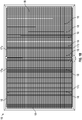
- Fig. 1A depicts a top view of a first type of solar module 10 formed from strings 11 of solar cells 12, wherein the strings 11 are interconnected electrically via conductive bus ribbons 13.
- the solar cells 12 are interconnected electrically via conductive tab ribbons 14.
- the electrically conductive ribbons, such as bus ribbons 13 and tab ribbons 14, are designed to carry the electric output produced by the solar cells 12 from one solar cell to another neighboring solar cell and/or from one string 11 to another neighboring string.
- the electrically conductive ribbons, such as bus ribbons 13 and tab ribbons 14 can be fixed to the solar cells or solar module by any suitable method known to those skilled in the art, including but not limited to the use of electrically conductive adhesives (ECAs) and/or the use of solders.
- ECAs electrically conductive adhesives
- the electrically conductive tab ribbons 14 are positioned across a central area of the solar cells 12 thereby being fully visible from a top surface of the solar cell and blocking some sunlight or shading some portion of the solar cells 12.
- the solar cells may be interconnected electrically via conductive tab ribbons (not shown) positioned on a bottom side of solar module 19 opposite the top side depicted in Fig. 1B .
- the electrically conductive ribbons, such as bus ribbons 17a-d and tab ribbons, are designed to carry the electric output produced by the solar cells from one solar cell to another neighboring solar cell and/or from one strip to another neighboring strip and/or from one string to another string.
- the electrically conductive ribbons such as bus ribbons 17a-d and the tab ribbons, can be fixed to the solar cells or solar module by any suitable method known to those skilled in the art, including but not limited to the use of electrically conductive adhesives (ECAs) and/or the use of solders.
- ECAs electrically conductive adhesives
- Electrically conductive ribbons for solar cells or modules are commonly made from metallic materials.
- suitable metallic materials which efficiently conduct electricity include copper, gold, silver, tin, iron, nickel, lead, and the like.
- the conductive ribbons may be coated with metal alloys which will not only protect the copper but also provide better bonding to the solar cells.
- the metal alloys include, but are not limited to, Pb/Sn, Pb/Sn/Ag, Sn/Ag, Bi/Sn/Ag, etc.
- the ribbons are great for conducting electricity but are solid pieces of metal which can shade at least a portion of the solar cell or module and further can be easily soiled with contaminants during processing. Contaminants on the bottom side or inwardly facing side of the ribbon can decrease the surface area of the electrical contact points between the ribbon and the solar cell, the solar module, and/or other ribbons, thereby decreasing the efficiency of the ribbon to conduct electricity.
- the ribbons are not aesthetically pleasing because the uncoated ribbons may stand out against and/or may be in stark contrast to, the black or blue background of the average solar cell or module.
- a colored conductive ribbon(s) can be manufactured from at least the steps provided.
- at least one conductive ribbon is combined with a channeled ribbon holder and a color coating is applied to at least one side of the conductive ribbon.
- the color coating is also applied to at least some portion of the channeled ribbon holder.
- the coating is applied only to the top side of the ribbon.
- the color coating is applied by placing the combined conductive ribbon and ribbon holder into a coating device, i.e., a screen-coater, roll-coater, or spray-coater, and the color coating is screened, sprayed, and/or rolled onto at least the top surface of the conductive ribbon.
- the color coating on the conductive ribbon is then cured to form a colored conductive ribbon on at least one side, i.e., the top side facing outward from the channel, and the conductive ribbon is separated from the channeled ribbon holder.
- the present process is intended to leave a bottom side, i.e., the side opposite the top side, of the conductive ribbon uncoated.
- the uncoated bottom surface will be the surface on which the conductive ribbons described herein will be attached to the solar cells, solar modules, and/or other ribbons.
- the color coating is cured using a heating process. In some embodiments, the color coating is cured using a UV process.
- the coating is cured and then separated from the ribbon holder.
- this may be in a reel to reel processing scenario where the ribbon is constantly fed through the ribbon holder as it is unwound from a reel of ribbon material and wound onto a new reel of coated ribbon material.
- the ribbon may be separated from the ribbon holder before and/or during the curing process.
- a color-coating is intended to encompass a composition including at least one color, pigment, and/or dye. It is envisioned that any color may be used. However, some particularly embodiments, the color-coating may be a composition which renders the conductive ribbons black, such as black paint or ink. In some other particular embodiments, the color-coating may be a composition which renders the conductive ribbons white, such as white paint or ink.
- the paint may be an electrically conductive paint, i.e., BARE® conductive electric paint. In embodiments, the paint may be a thermally insulative paint. In embodiments, the color coating may form a textured coating suitable for improving the amount of light reflected from the ribbons back to the solar cells.
- the color coatings described herein may include various other ingredients commonly associated with color coatings, such as binders, extenders, solvents, volatile organic compounds, dispersants, thixotropic agents, driers, bactericides, fungicides, algaecides, fragrances, and combinations thereof.
- the color coating is a liquid.
- the color coating is a powder.
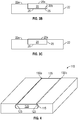
- the ribbon holder 22 includes at least one channel 25 dimensioned and configured to receive the at least one conductive ribbon 20.
- the channel includes a channel length, channel width, and/or channel depth generally equal to the ribbon length, ribbon width, and/or ribbon height of the conductive ribbon 20 thereby ensuring a suitably snug yet removable fit of the ribbon 20 within the channel 25.
- the ribbon holder 22 includes a holder length, holder width, and holder height, wherein at least the holder width and holder height of the holder 22 is greater than the ribbon width and ribbon height of ribbon 20.
- the channel depth of channel 25 may be less than the ribbon height of the conductive ribbon 20, which may assist in limiting the application of the color coating to only the conductive ribbon 20 (and not the ribbon holder 22) because the top surface 20a of the conductive ribbon 20 will extend beyond the top surface 22a of the holder 22.
- the channel 25 may include a pair of sidewalls 25a, 25b which define the channel depth by extending from the top surface 22a of the ribbon holder 22 to the bottom surface 25c of the channel 25.
- the sidewalls 25a, 25b may be generally parallel to each other and connected to each other via the base surface 25c of the channel 25 which may be generally perpendicular to the sidewalls 25a, 25b. It is envisioned however, that in some other embodiments, the sidewalls may not be generally parallel to each other and/or the base surface may not be generally perpendicular thereto.
- the ribbon holders, channels, and/or conductive ribbon may of any shape suitable for performing the methods described herein.
- the base surface 25c may includes an adhesive 26 for removably or temporarily securing the conductive ribbon 20, particularly the bottom surface 20b of the conductive ribbon 20, within the channel 25 during the coating processes described herein.
- the coating can also operate as an overspray barrier preventing adhesion of any of the coating on the uncoated surface of the ribbon.
- the bond strength is configured to be sufficient to withstand the forces applied thereto during any coating and/or curing processes, while remaining configured to be broken by forces slightly higher than those applied during the coating and/or curing processes, so the ribbon can eventually be removed from the channel fairly easily.
- the adhesive layer may be readily removed from the underside of the ribbon using one or more solvents, even water, to ensure a clean surface for eventual bonding with the strings 11 and electrical conduction therethrough.
- the adhesive may be selected to have a greater adhesion to the holder than the ribbon and thus remain in place when the ribbon is removed from the holder, and the solvents may be applied to the holder to remove the adhesive.
- suitable adhesives include pressure sensitive adhesives, hot-melt adhesives, dissolvable adhesives, reactive adhesives, two-part adhesives, synthetic adhesives, bioadhesives, and combinations thereof.
- the adhesive is a pressure sensitive adhesive.
- Some pressure sensitive adhesives may include of an elastomer, such as natural rubber, vinyl ethers, acrylics, butyl rubber, styrene block copolymers, silicones and nitriles.
- the pressure sensitive adhesive may be selected based on the adhesive's adhesion strength over a certain period of time.
- the pressure sensitive adhesive may be a peelable PSA wherein the adhesive is intended to be removed at some point of time without damaging the ribbon and/or the ribbon holder.
- Other non-limiting examples include high-tack PSAs, permanent PSAs, and/or freezer PSAs.
- the adhesive 26 may prevent and/or remove possible contaminants from the bottom surface 20b of the conductive ribbon 20 when the ribbon is removed from the channel.
- any contaminants on the bottom surface of the ribbon may become secured to the adhesive during the coating and/or curing processes described herein and remain adhered to the adhesive when the ribbon is separated from the channel thereby providing a top side of the ribbon which is color coated and bottom side of the ribbon including a reduced amount of contaminants and/or free of any contaminants.
- a ribbon holder 110 is depicted including a channel 115 in receipt of a conductive ribbon 120 and a pair of masking tabs 130a, 130b.
- Masking tabs 130a, 130b define an opening 135 having an opening width less than the channel width.
- Such a configuration allows the masking tabs 130a, 130b to prevent some portions, in this instance the outer edges 123 of the top surface 122 of the conductive ribbon 120 from receiving any color coating during the application process.
- the edges of the masking tabs 130a, 130b may be the same or different and may be of any shape or configuration, i.e., rounded, sinusoidal, jagged, etc.
- the masking tabs may be made from the same material used to form the ribbon holder. In some embodiments the masking tabs may be added to the ribbon holder separately. In some embodiments, the masking tabs may be removable and/or replaceable from the ribbon holder. In some embodiments, the masking tabs may be made from a paper, rubber, silicone, or plastic material suitable for preventing the color coating material from being applied to at least a portion of the conductive ribbon.
- the ribbon holder can be a single layer of sheet material, i.e., a single sheet.
- the ribbon holder can be formed of multiple layers of sheet material, i.e., multiple sheets.
- the ribbon holders described regardless of layers may be made from any material suitable for securing the ribbon during the coating and/or curing processes described herein.
- the ribbon holder may be made from plastic or polymeric materials which can be molded, pressed, extruded, and the like to form the overall shape of the holder.
- the ribbon holder maybe made from paper and/or paper-like products such as cardboard.
- the channeled ribbon holder may be formed from any suitable molding, extruding, and/or pressing process.
- the channel of the ribbon holder of a single sheet may be formed after formation of the ribbon holder, i.e., by cutting out material from the ribbon holder to form the channel.
- the ribbon holder 210 include at least one masking sheet 212 positioned directly on top a base sheet 211 including and/or coated with an adhesive 225.
- Ribbon holder 210 includes channel 215 formed in or by the at least one masking sheet 212.
- a plurality of masking sheets may be positioned directly upon base sheet 211 in a spaced apart configuration creating gaps or channels between each of the masking sheets and leaving a portion of the base sheet exposed or uncovered creating the channel therebetween.
- a single masking sheet 212 may be positioned directly upon base sheet 211 and then the masking sheet may be cut to remove a portion of the masking sheet from the base sheet 211 thereby creating the channel 215.
- the ribbon holder includes one channel or at least one channel. In other embodiments, the ribbon holder includes multiple channels, which in turn may receive multiple conductive ribbons. In embodiments, one channel receives one ribbon.
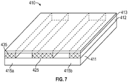
- the ribbon holders 310, 410 may be formed from two or more sheets, and particularly, three sheets, i.e., base sheet 311, 411, masking sheet 312, 412, and protective sheet 313, 413.
- the masking sheets 312, 412 are positioned directly on top a base sheet 311, 411 via an adhesive 325, 425 and form channels 315, 415a, 415b.
- the protective sheets 313, 413 are positioned directly on a top of masking sheets 312, 412 via adhesive 335, 435 and the protective sheets 313, 413 are intended to at least prevent premature access to the channels 315, 415a, 415b to the ribbons and/or contaminants.
- the protective sheet 313, 413 may be combined with the masking sheet 312, 412 to predetermine the width of the channels 315, 415a, 415b prior to be adding to the base sheet 310, 410.
- the protective sheet is typically removed from the masking sheet after formation of the channel and prior to receipt of the conductive ribbon within the channel.
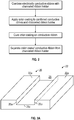
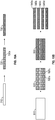
- a process is illustrated for forming a colored conductive ribbon as described herein.
- a base sheet 511 including a top surface coated with an adhesive is combined with a masking sheet 512, and particularly, the masking sheet 512 covers a majority, if not the entire, base sheet 511.
- the masking sheet 512 is cut to remove a portion of the masking sheet 512 thereby creating a channel 515.
- the masking sheet may be cut using any suitable method. Some non-limiting examples include cutting with a laser, a knife, a blade, ultrasonics, a press, scissors, and the like.
- a conductive ribbon 520 is positioned and/or secured within the channel 515 and the sidewalls are formed from the remaining portions of the masking sheet 512.
- the conductive ribbon 520 is secured in the channel 515 via the adhesive positioned on the top surface of the base sheet 511. It is envisioned that in some instances, the adhesive may be reapplied to the base surface of the channel upon removal of the cut piece of the masking sheet and prior to receipt of the ribbon, as removal of the cut piece may also remove some of the adhesive originally positioned on the base sheet.
- the top surface of the conductive ribbon 520 is uncolored and/or displays a metallic finish prior to coating.
- a color coating is applied to the conductive ribbon 520 secured in the channel 515 of the ribbon holder 513, the color coating on the conductive ribbon 520 is cured, and the color coated conductive ribbon is separated from the channel of the ribbon holder.
- the color coated conductive ribbon 520 is physically separated from the channel 515 of the ribbon holder 513 after curing.
- the cured color coated conductive ribbon 520 can be peeled away from the channel 515, and more particularly peeled away from the adhesive on the top surface of the base sheet 511. In such instances, once the ribbon is peeled away from the ribbon holder, no portion of the ribbon holder remains in contact with the ribbon.
- the color coated conductive ribbon 520 is physically separated from the ribbon holder 513 by cutting or punching the ribbon 520 free of the ribbon holder 513.
- the base sheet 511 may also be cut or punched free of the ribbon holder 513 and remain adhered to ribbon 520 thereby leaving the ribbon 520 adhered to at least a portion, if not all, of the base sheet 511.
- the colored conductive ribbon may be a solid ribbon 520a or a ribbon including pores 520b. It is envisioned that the pores may be added at any time during the processes described herein. For example, in some embodiments, the pores may be added to the conductive ribbons prior to entering the channel. In such embodiments, the color coating, when applied, may not only cover the top surface of the ribbon but also some portion, if not all, of the inner wall of the pore defined in the thickness of the ribbon.
- the pores may be added to the conductive ribbon after the coating is applied. In still other embodiments, the pores may be added to the conductive ribbon after the curing of the coating and/or upon separation of the ribbon from the channel. In such embodiments, the inner walls of the pores may not include the color coating.
- the pores may be symmetrically distributed across the ribbon.
- the pores may be non-symmetrically distributed across the ribbon.
- the pores may be closer to one edge of the ribbon than another edge of the ribbon. Due to the non-symmetrical distribution of the pores, the surface area of the ribbon which is adhered to the base sheet 511 may not be evenly distributed. Removal of the adhered base sheet 511 will cause the ribbon to produce a curved surface because the peeling force of the base sheet 511 cannot be evenly distributed across the ribbon due to the asymmetrical pores. Therefore, in such embodiments, it may be beneficial to remove the color coated ribbon completely from the base sheet 511 (as well as the channel or ribbon holder) prior to the formation of the asymmetrical pores to prevent curving or bowing of the non-symmetrical pored ribbon.
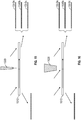
- Fig. 8B another process is illustrated for forming a colored conductive ribbon as described herein.
- a plurality of masking sheets 612a, 612b spaced apart from each other and secured to an outer protective sheet 613 via an adhesive are combined with a base sheet 610, the masking sheets 612a, 612b positioned between the protective sheet 613 and the base sheet 610.
- the protective sheet 613 temporarily covers the masking sheets 612a, 612b, the base sheet 610, and the channel 615. Once combined, the protective sheet 613 is removed from the masking sheets 612a, 612b to provide access to the channel 615.
- a conductive ribbon 620 is positioned and/or secured within the channel 615 via an adhesive and the sidewalls formed from the remaining portions of the masking sheets 612a, 612b.
- a color coating is applied to the conductive ribbon 620 secured in the channel 615 of the ribbon holder 614, the color coating on the conductive ribbon 620 is cured, and the color coated conductive ribbon is separated from the channel of the ribbon holder 614.
- FIGs. 8A and 8B depict processes utilizing a multilayer ribbon holder similar to those shown in Figs. 5 and 6 , it is envisioned that the processes of coating a conductive ribbon described in Figs. 8A and 8B may alternatively utilize a single layer ribbon holder, such as any of the ribbon holders shown in Figs. 3A , 3B, 3C, 4 and/or 7.
- the conductive ribbons may be coated in a manner generally as shown in Figs. 8A or 8B wherein the ribbon holder of Fig. 4 is utilized, as either a single or multilayer ribbon holder.
- the conductive ribbon 650, 660 is coated utilizing the ribbon holder of Fig. 4 to form a coated conductive ribbon 650a, 660a having first and second uncoated outer edge portions 653a, 653b, 663a, 663b which extend longitudinally along the length of the coated ribbon 650a, 660a.
- Uncoated outer edge portions 653a, 653b, 663a, 663b are positioned on either side of a coated central portion 655, 665.
- Uncoated outer edge portions 653a, 653b, 663a, 663b can be removed or separated from the coated central portion 655, 665 to form a coated conductive ribbon 650b, 670a, 670b, 670c including only coated central portion 655, 665.
- the uncoated outer edges 653a, 653b, 663a, 663b can be mechanically cut or separated from coated central portion 655, 665 using any suitable method, including but not limited to cutting with a blade, press, punch or laser.
- the outer edges of the conductive ribbon remain uncoated and prevent the coating from reaching the rear side of conductive ribbon during the coating and/or curing processes.
- the channel of the conductive ribbon of Fig. 4 may not include an adhesive and/or the rear side of the conductive ribbon of Figs. 9A and 9B may not be attached to an adhesive or tape during the coating process.
- the colored conductive ribbons may be a solid (free of pores) ribbon 520a, 620a, 670a, 670b, 670c, 655 or a ribbon including pores 520b, 620b, 650b, 675a, 675b, 675c.
- the pores may be added to the ribbon at any time during the processes described herein.
- the pores may be added to the conductive ribbons prior to entering the channel and/or prior to the application of the color coating.
- the coating composition when applied may not only cover the top surface of the ribbon but also some portion, if not all, of the inner wall of the pore defined in the thickness of the ribbon.
- the pores may be added to the conductive ribbon after the color coating is applied and/or cured. In still other embodiments, the pores may be added to the conductive ribbon after the curing of the coating and/or upon separation of the ribbon from the channel. In such embodiments, the inner walls of the pores may not include the color coating.
- an electrically conductive ribbon 655, 665, 710 free of pores (solid) may be processed in some manner to include pores.
- the pores are formed via a punching process.
- the process of punching or removal of some portion of the conductive ribbon to form the pores can be performed in several ways, such as a mechanical punching processes or laser ablation/cutting processes.
- the pores may be created with a punch.
- the punched conductive ribbon may be coated via one of the processes described herein.
- the punched conductive ribbons may be coated with a color coating, i.e., a black paint or composition, and cured to produce a colored and/or black conductive ribbon.
- the conductive ribbon that is processed may have a sufficient width that following the coating processes described herein, the colored conductive ribbon can be then sliced into a plurality of thinner strips having a smaller width suitable as either a tabbing ribbon or bus ribbon.
- an extra wide electrically conductive ribbon 810 free of pores may be processed in some manner to include pores.
- the pores are formed via a punching process.
- the process of punching or removal of the some portion of the conductive ribbon to form the pores can be performed in several ways, such as a mechanical punching processes or a laser ablation processes.
- the pores may be created with a punch.
- the punched conductive ribbon 820 may be coated via one of the processes described herein with a color coating. As specifically shown in Fig.
- the punched conductive ribbon 820 may be coated with a color coating, i.e., a black paint or composition, and cured to produce a colored and/or black conductive ribbon 830.
- the colored and/or black conductive ribbon may then be sliced into a plurality of thinner strips having a smaller width 840a-d.
- the step of slicing may be performed using a plurality of lasers, knives, blades, ultrasonics, presses, scissors, and combinations thereof.
- an electrically conductive ribbon 910 free of pores (solid) may be coated via one of the processes described herein with a color coating. Once coated and/or cured, the color coated conductive ribbon may be processed in some manner to include pores. In embodiments, the pores are formed via a punching process. The process of punching or removal of the some portion of the coated conductive ribbon to form the pores can be performed in several ways, such as a mechanical punching processes or a laser ablation processes. In particular embodiments, the pores may be created with a punch.
- the conductive ribbon 910 may be coated with a color coating, i.e., a black paint or composition, and cured to produce a colored and/or black conductive ribbon 920, which can subsequently be punched to form pores within the coated conductive ribbon forming a color coated porous conductive ribbon and/or a black coated porous conductive ribbon 930.
- a color coating i.e., a black paint or composition
- the conductive ribbon 950 that is processed may have a sufficient width that following the coating processes described herein, the colored conductive ribbon 950 can be then sliced into a plurality of thinner strips having a smaller width suitable as either a tabbing ribbon or bus ribbon.
- an extra wide electrically conductive ribbon 950 free of pores (solid) may be coated with a color coating, i.e., a black paint or composition, and cured to produce a colored and/or black conductive ribbon 960.
- the colored and/or black conductive ribbon 960 may be processed in some manner to include pores.
- the pores are formed via a punching process. The process of punching or removal of the some portion of the conductive ribbon to form the pores can be performed in several ways, such as a mechanical punching processes or a laser ablation processes. In particular embodiments, the pores may be created with a punch.
- the punched colored conductive ribbon 970 may be sliced into a plurality of thinner strips having a smaller width 980a-d.
- the step of slicing may be performed using a plurality of lasers, knives, blades, ultrasonics, presses, scissors, and combinations thereof coated via one of the processes described herein with a color coating.
- the colored and/or black conductive ribbon 960 may be sliced into a plurality of thinner strips having a smaller width 975a-d prior to being made to include pores, i.e., punched. Once sliced into thinner strips, the plurality of strips may be collectively or individually processed to include pores, i.e., punched, to form punched strips of colored conductive ribbons 980e-h.
- the conductive ribbons described herein may be roughened, at anytime during the manufacturing process, to add a textured surface to at least a portion of the ribbon surface.
- a textured surface By adding a textured surface to the ribbon, the bond strength or peeling strength of the ribbon is greatly improved when adhered or bonded to a solar cell (including solar strips or solar modules) along the textured portion of the ribbon.
- the ribbons may be roughened to include a textured surface prior to coating. In some embodiments, the ribbons may be roughened to include a textured surface after coating.
- the textured surface may be continuous or discontinuous along any outer surface of the ribbon. In some embodiments, the textured surface is only on portions of the outer surface of the ribbon which are not coated. In some embodiments, the textured surface is only on coated portions of the outer surface of the ribbon. In some embodiments, the textured surface is on coated portions and non-coated portions of the outer surface of the ribbon.
- the conductive ribbon 1210 can be passed between at least one roughening element 1220 and a generally flat hard surface 1230 to produce a textured surface 1240a-c on at least one surface of the conductive ribbon 1210.
- the roughening element 1220 is a roller which rotates as indicated by the arrow forcing outer surface 1221 of the roller 1220 against a first surface 1210b of ribbon 1210 to roughen the surface creating a texture.
- the conductive ribbon 1210 either coated or uncoated, may initially have a smooth non-textured surface 1210a prior to passing by the roughening element 1220.
- the roughening element 1220 having an outer surface 1221 configured to roughen smooth surface 1220a against hard surface 1230 to produce a textured surface 1240a-c on at least a first side 1210b of ribbon 1210.
- the texture of the textured surface may be random (surface 1240a) or patterned (surface 1240b, 1240c) of various depths.
- the roughening element 1220 may include an outer surface 1221 including a patterned coarseness which when applied to the ribbon 1210, under the correct conditions, i.e., pressure, temperature, length of time, etc., transfers the mirror image of the patterned coarseness to at least a first side 1210b of ribbon 1210.
- any of the roughening processes described herein may include multiple passes of the ribbon over the roughening element and/or in any number of directions.
- the conductive ribbon 1210 can be passed between a plurality of roughening elements 1220, 1222 to produce a textured surface 1245a-c on at least two surfaces of the conductive ribbon 1210.
- the two surfaces being opposite each other, such as a top and bottom surface.
- Roughening elements 1220, 1222 are depicted as rollers which rotate as indicated by the respective arrows forcing outer surfaces 1221, 1223 of the rollers 1220, 1222 against a first smooth surface 1210b and a second smooth surface 1215b of ribbon 1210 to roughen the ribbon on multiple surfaces creating a texture thereon.
- the conductive ribbon 1210 may initially have a generally smooth non-textured surface 1210a, 1215a prior to passing by the roughening element 1220, 1222 to produce a dual-sided textured ribbon including first textured surface 1210b and second textured surface 1215b.
- the conductive ribbon 1310 can be passed between a press 1330 and at least one roughening element 1320, such as a textured linear surface, to produce a textured surface 1340a-c on at least one surface of the conductive ribbon 1310.
- the textured linear surface of roughening element 1320 may be stationary while the press 1330 is configured to move or slide (as indicated by the arrow) towards the roughening element 1320 while the ribbon 1310 is positioned therebetween.
- the press may also a textured surface configured to roughen a second surface opposite the first surface.
- both the press and the roughening element are configured to move or slide towards each other with the ribbon positioned therebetween.
- the conductive ribbon 1410 can be ground over a textured linear roughening element 1420, such as an emery board, emery stone or grinding tool, to produce a textured surface 1440a-b on at least one surface of the conductive ribbon 1410.
- a textured linear roughening element 1420 such as an emery board, emery stone or grinding tool
- at least one of the roughening element 1420 or ribbon 1410 are moved relative to the other under pressure to roughen the surface of the ribbon 1410.
- the roughening element 1520 is a laser device configured to laser scan or carve the textured surface 1540a-c onto at least one side 1510a of the conductive ribbon 1510.
- the laser device 1520 is movable in any direction, i.e., forward, back, up, down, side-to-side, etc., relative to the ribbon 1510 which may be stationary. Although depicted on only one side of the ribbon, it is envisioned that laser device may be positioned on multiple sides of the ribbon.
- the roughing element 1620 does not roughen the surface of ribbon 1610 by removing material. Rather, roughening element 1620 is configured to add material, such as particles or sand, to the surface of the ribbon 1610 to create a textured surface 1640a-c.
- the roughening element 1620 is a sand blaster capable of moving in any direction, i.e., forward, back, up, down, side-to-side, etc., relative to the ribbon 1610 which may be stationary. Although depicted on only one side of the ribbon, it is envisioned that the sand blaster may be positioned on multiple sides of the ribbon.
- the textured surfaces as described herein can create a roughness creating grooves, channels, dimples, crevices, etc. having a depth ranging from 0.01 microns to 1000 microns.
- the depth of the roughness may range from about 0.1 microns to 500 microns.
- the depth of the roughness may range from about 1 micron to 250 microns.
- the depth of the roughness may range from about 10 microns to 100 microns.
- the textured surface as described herein can improve the bonding strength or peeling strength between the coated ribbon and the solar cell by a range of 0.1N to IN. In some embodiments, by a range of 0.2N to 0.5N. In some embodiments, by a range from 0.3N to 0.4N.
- the present disclosure describes a solar module including a plurality of strings of solar cells, each string including an array of shingled strips of solar cells, and at least one electrically conductive bus ribbon connected to the plurality of strings, wherein the at least one electrically conductive bus ribbon includes a color coating on at least a first outer surface of the bus ribbon.
- the electrically conductive ribbon may soldered to the strings of the solar module and/or may be adhered to the strings of the solar module using known electrically conductive adhesives.
- the color coating is on top surface of the ribbon. In some embodiments, the color coating is both the top and opposite bottom surfaces of the ribbon.
- the color coating on the ribbon is a black composition.
- the black composition is a black paint.
- the black paint is an electrically conductive black paint.
- the color coating is on a central portion of the electrically conductive ribbon, the central portion extending longitudinally along a length of the electrically conductive ribbon with uncoated first and second outer edges extending longitudinally along the length of the electrically conductive ribbon and positioned on either side the central portion.
- At least a second outer surface opposite the first outer surface is free of contaminants after the first surface is colored with the color coating composition.
- the electrically conductive ribbon further includes a plurality of pores.
- the plurality of pores are asymmetrically distributed across the ribbon.
- At least a second outer surface opposite the first outer surface includes a textured surface.
- the textured surface includes a roughness having a depth from about 0.01 to about 1000 microns.
- the textured surface increases the bonding strength between the electrically conductive ribbon and the string of solar cells of from about 0.3N to 0.4N.
- identification labels In addition to electrically conductive materials, some additional materials which may be frequently attached to the top surfaces of a solar cell or module include for example identification labels.
- identification labels such as bar codes or QR codes, are often applied to each of the individual solar cells or solar modules to ensure the authenticity of the source of the solar cells or modules.
- these labels are often predominantly white which, like metallic conductive ribbons, can not only stand out aesthetically when placed on a black solar cell or module, but further may provide small areas of shading on the cells or modules.
- the labels may be colored, such as black or blue, to match the solar cell or module and the bar code or QR code information may be printed using a different color coating composition, i.e., ink.
- a black label may be processed as described herein to be coated with a white ink wherein the white ink represents the bar code information and the black label is the background.
- the black and white portions of the usual bar code or QR code are reversed rendering most of the label black and a minority of the label white, thereby allowing a majority of the label to blend with the solar cell or module surface.
- Another option to obtaining the same label effect may include starting with the normal white labels and applying a black coating as described herein.
- the coating may be applied to form an outline or stencil of the bar code or QR code information, i.e., reverse print the code information.
- the white label would show through the black outlined coating as the bar code or QR code information.
- the black and white portions of the usual bar code or QR code are reversed rendering most of the label black and a minority of the label white, thereby allowing a majority of the label to blend with the solar cell or module surface.
Landscapes
- Photovoltaic Devices (AREA)
- Engineering & Computer Science (AREA)
- Life Sciences & Earth Sciences (AREA)
- Sustainable Development (AREA)
- Manufacturing & Machinery (AREA)
- Chemical & Material Sciences (AREA)
- Crystallography & Structural Chemistry (AREA)
- Application Of Or Painting With Fluid Materials (AREA)
- Sustainable Energy (AREA)
- Paints Or Removers (AREA)
Description
- The present disclosure relates to solar modules, and more particularly, to solar modules including improved efficiency and aesthetics by including colored electrically conductive ribbons, or other materials that can be attached directly to the solar cells and/or solar modules, which can be formed from the methods described herein.
- Over the past few years, the use of fossil fuels as an energy source has been trending downward. Many factors have contributed to this trend. For example, it has long been recognized that the use of fossil fuel-based energy options, such as oil, coal, and natural gas, produces gases and pollution that may not be easily removed from the atmosphere. Additionally, as more fossil fuel-based energy is consumed, more pollution is discharged into the atmosphere causing harmful effects on life close by. Despite these effects, fossil-fuel based energy options are still being depleted at a rapid pace and, as a result, the costs of some of these fossil fuel resources, such as oil, have risen. Further, as many of the fossil fuel reserves are located in politically unstable areas, the supply and costs of fossil fuels have been unpredictable.
- Due in part to the many challenges presented by these traditional energy sources, the demand for alternative, clean energy sources has increased dramatically. To further encourage solar energy and other clean energy usage, some governments have provided incentives, in the form of monetary rebates or tax relief, to consumers willing to switch from traditional energy sources to clean energy sources. In other instances, consumers have found that the long-term savings benefits of changing to clean energy sources have outweighed the relatively high upfront cost of implementing clean energy sources.
- One form of clean energy, solar energy, has risen in popularity over the past few years. Advancements in semiconductor technology have allowed the designs of solar modules and solar panels to be more efficient and capable of greater output. Further, the materials for manufacturing solar modules and solar panels have become relatively inexpensive, which has contributed to the decrease in costs of solar energy. As solar energy has increasingly become an affordable clean energy option for individual consumers, solar module and panel manufacturers have made available products with aesthetic and utilitarian appeal for implementation on residential structures. As a result of these benefits, solar energy has gained widespread global popularity.
- Patent document
US 2015 349145 A1 discloses colored conductive ribbons designed to improve visual contrast between solar cells and the back sheet of solar modules.Patent document DE 10 2010 004112 A1 discloses a method of manufacturing conductive ribbons for solar cell interconnection within a solar module. - The present disclosure provides solar modules and/or solar cells including electrically conductive ribbons which are color-coated on at least one side. In addition, methods of manufacturing such color-coated electrically conductive ribbons, or other materials that ma attached directly thereto, are also provided.
- The present invention relates to methods of manufacturing a colored conductive ribbon for a solar module according to the appended claims.
- In embodiments, methods of forming a colored conductive ribbon for a solar module are provided which include the steps of: a) providing a ribbon holder including a channel configured to receive a conductive ribbon therein, b) securing the conductive ribbon in the channel of the ribbon holder, c) applying a color coating to at least the conductive ribbon secured within the channel, d) curing the color coating on the conductive ribbon, and e) separating the conductive ribbon from the channel of the ribbon holder.
- In embodiments, the color coating may be a black composition or paint.
- In embodiments, the color coating may be thermally insulative or electrically conductive.
- In embodiments, the step of applying the color coating in c) maybe performed by at least one method selected from screen-coating, roll-coating, or spray-coating.
- In embodiments, the step of curing the color coating in d) may be performed by heat-curing or UV (ultraviolet light) curing.
- In embodiments, the step of removing the conductive ribbon in e) may occur prior to the curing of the color coating in step d).
- In embodiments, the ribbon may be secured in the channel by an adhesive positioned in the channel to temporarily fix the ribbon to the holder during the coating method provided herein. In such embodiments, the adhesive is configured to additionally remove contaminants from the bottom surface of the conductive ribbon when the conductive ribbon is separated from the temporary hold of the adhesive thereby releasing the ribbon from the channel and/or holder.
- In embodiments, the ribbon may include pores, the pores may be added to the ribbon before or after the coating methods described herein. In embodiments, the pores may be formed by exposing the ribbons to a punching process.
- In some embodiments, the methods described herein for forming a color conductive ribbon for a solar module include: a) securing a top surface of a base sheet, the top surface including an adhesive material, to a bottom surface of a masking sheet, b) forming a channel configured to receive a conductive ribbon in at least the masking sheet to form a ribbon holder, c) securing the conductive ribbon in the channel of the ribbon holder, d) applying a color coating to at least the conductive ribbon secured within the channel, e) curing the color coating on the conductive ribbon, and f) separating the conductive ribbon from the channel of the ribbon holder.
- In still other embodiments, the methods described herein for forming a color conductive ribbon for a solar module include the steps of: a) securing a top surface of a masking sheet, the top surface including an first adhesive material, to a bottom surface of a handling sheet, b) securing a top surface of a base sheet, the top surface including an second adhesive material, to a bottom surface of the masking sheet, c) forming a channel configured to receive a conductive ribbon in at least the masking sheet to form a ribbon holder, d) securing the conductive ribbon in the channel of the ribbon holder, e) applying a color coating to at least the conductive ribbon secured within the channel, f) curing the color coating on the conductive ribbon, and g) separating the conductive ribbon from the channel of the ribbon holder.
- Furthermore, the present disclosure includes the following further aspects and embodiments:
- According to a first aspect a method of forming a colored conductive ribbon for a solar module is provided, comprising the steps of: a) providing a ribbon holder including a channel configured to receive a conductive ribbon therein, b) securing the conductive ribbon in the channel of the ribbon holder, c) applying a color coating to at least the conductive ribbon secured within the channel, d) curing the color coating on the conductive ribbon, and e) separating the conductive ribbon from the channel of the ribbon holder.
- According to another aspect depending on the first aspect the color coating may be a black composition.
- According to another aspect depending on the afore-mentioned aspect the black composition may be a black paint.
- According to another aspect depending on the afore-mentioned aspect the black paint may be an electrically conductive black paint.
- According to another aspect depending on the first aspect the ribbon holder may include a single layer of sheet material.
- According to another aspect depending on the first aspect the ribbon holder may include multiple layers of sheet material.
- According to another aspect depending on the afore-mentioned aspect the multiple layers of the ribbon holder may include a base sheet including a top surface including an adhesive material and a masking sheet including a bottom surface secured the top surface of the base sheet by the adhesive material.
- According to another aspect depending on the afore-mentioned aspect the channel may have a depth defined by a thickness of the masking sheet and/or the multiple layers of the ribbon holder may further include a protective sheet removably attached on a top surface of the masking sheet and free of a channel.
- According to another aspect depending on the first aspect the channel may include a base surface including an adhesive for securing the conductive ribbon within the channel during temporarily.
- According to another aspect depending on the afore-mentioned aspect the adhesive may remove contaminants from a bottom surface of the conductive ribbon when separating the conductive ribbon from the channel of e).
- According to another aspect depending on the first aspect the channel may have a channel depth which is less than or equal to a thickness of the conductive ribbon.
- According to another aspect depending on the first aspect the ribbon holder may include a pair of masking tabs positioned at a top side of the channel and having an opening width that is less than the opening width of the channel.
- According to another aspect depending on the afore-mentioned aspect a color coated ribbon may be formed having a coated central portion extending longitudinally along a length of the ribbon and first and second uncoated outer edges extending longitudinally along a length of the ribbon and positioned on either side the coated central portion.
- According to another aspect depending on the first aspect applying the color coating of c) may include at least one of screen-coating, roll-coating, or spray-coating.
- According to another aspect depending on the first aspect curing the color coating of d) may include heat-curing or UV curing.
- According to another aspect depending on the first aspect removing the conductive ribbon of e) may occur prior to curing the color coating of d).
- According to another aspect depending on the first aspect the method may further comprise step of punching the conductive ribbon to include a plurality of pores.
- According to another aspect depending on the afore-mentioned aspect the plurality of pores may be asymmetrically distributed across the ribbon and/or the step of punching the conductive ribbon may occur prior to securing the conductive ribbon in the channel of b) or after removing the conductive ribbon from the channel of e).
- According to another aspect depending on the first aspect the method may further comprise a step of slicing the conductive ribbon into thinner strips.
- According to another aspect depending on the afore-mentioned aspect the step of slicing the conductive ribbon into thinner strips may occur prior to securing the conductive ribbon in the channel of b) or after removing the conductive ribbon from the channel of e).
- According to another aspect depending on the first aspect the step of removing the conductive ribbon of e) may occur prior to curing the color coating of d).
- According to another aspect depending on the first aspect the method may further comprise a step of roughening at least a portion of the conductive ribbon to add a textured surface to the ribbon.
- According to another aspect depending on the afore-mentioned aspect the step of roughening of the conductive ribbon may include passing the conductive ribbon over at least one roughening element.
- According to another aspect depending on the afore-mentioned aspect the at least one roughening element may be at least one roller having an outer surface configured to roughen an outer surface of the ribbon and/or the at least one roughening element may be a pair of rollers having an outer surface configured to roughen an outer surface of the ribbon, wherein the ribbon is passed between the two rollers. Additionally or alternatively the at least one roughening element may also include a textured linear surface and the conductive ribbon may be pressed against the textured linear surface by a press producing the textured surface on the ribbon. Additionally or alternatively the at least one roughening element may be selected from a group consisting of an emery board, an emery stone, and a grinding tool and/or the at least one roughening element may be a laser device configured to carve the textured surface onto at least one side of the conductive ribbon. Additionally or alternatively the at least one roughening element may be a sand blaster.
- In case the method according to the first aspect comprises the step of roughening at least a portion of the conductive ribbon to add a textured surface to the ribbon, the textured surface may - according to another aspect - include a roughness having a depth from about 0.01 to about 1000 microns and/or include a bonding strength between the ribbon and a solar cell of from about 0.3N to 0.4N.
- According to a second aspect a method of forming a colored conductive ribbon for a solar module is provided, comprising the steps of: a) securing a top surface of a base sheet, the top surface including an adhesive material, to a bottom surface of a masking sheet, b) forming a channel configured to receive a conductive ribbon in at least the masking sheet to form a ribbon holder, c) securing the conductive ribbon in the channel of the ribbon holder, d) applying a color coating to at least the conductive ribbon secured within the channel, e) curing the color coating on the conductive ribbon, and f) separating the conductive ribbon from the channel of the ribbon holder.
- According to another aspect depending on the second aspect the step of forming a channel of b) may include cutting and removing at least a portion of the masking sheet.
- According to another aspect depending on the afore-mentioned aspect the method may further comprise the step of removably attaching a bottom surface of a protective sheet to a top surface of the masking sheet prior to a).
- According to a third aspect a method of forming a colored conductive ribbon for a solar module is provided, comprising the steps of: a) securing a top surface of a masking sheet, the top surface including an first adhesive material, to a bottom surface of a handling sheet, b) securing a top surface of a base sheet, the top surface including an second adhesive material, to a bottom surface of the masking sheet, c) forming a channel configured to receive a conductive ribbon in at least the masking sheet to form a ribbon holder, d) securing the conductive ribbon in the channel of the ribbon holder, e) applying a color coating to at least the conductive ribbon secured within the channel, f) curing the color coating on the conductive ribbon, and g) separating the conductive ribbon from the channel of the ribbon holder.
- According to a fourth aspect a solar module is provided, comprising a plurality of strings of solar cells, each string including an array of shingled strips of solar cells, and at least one electrically conductive bus ribbon connected to the plurality of strings, wherein the at least one electrically conductive bus ribbon includes a color coating on at least a first outer surface of the bus ribbon.
- According to another aspect depending on the fourth aspect the color coating may be a black composition.
- According to another aspect depending on the afore-mentioned aspect the black composition may be a black paint.
- According to another aspect depending on the afore-mentioned aspect the black paint may be an electrically conductive black paint.
- According to another aspect, preferably depending on the fourth aspect, the color coating may be on a central portion of the electrically conductive ribbon, the central portion extending longitudinally along a length of the electrically conductive ribbon with uncoated first and second outer edges extending longitudinally along the length of the electrically conductive ribbon and positioned on either side the central portion.
- According to another aspect, preferably depending on the fourth aspect, the at least a second outer surface opposite the first outer surface may be free of contaminants after the first surface is colored with the coating composition.
- According to another aspect, preferably depending on the fourth aspect, the electrically conductive ribbon further may include a plurality of pores.
- According to another aspect depending on the afore-mentioned aspect the plurality of pores may be asymmetrically distributed across the ribbon.
- According to another aspect, preferably depending on the fourth aspect, the at least a second outer surface opposite the first outer surface may include a textured surface.
- According to another aspect depending on the afore-mentioned aspect the textured surface may include a roughness having a depth from about 0.01 to about 1000 microns and/or the textured surface may increase the bonding strength between the electrically conductive ribbon and the string of solar cells of from about 0.3N to 0.4N.
- According to another aspect, preferably depending on the fourth aspect, the solar module may further comprise at least one identification label which is predominantly not white.
- According to another aspect depending on the afore-mentioned aspect the identification label may be a black label coated with a white ink, wherein the white ink represents bar code information and the black label is a background or the identification label may be a white label coated with a black ink, wherein the black ink represents a black outline of a bar code and the white label shows through the black outline representing the bar code information.
- Various aspects of the present disclosure are described hereinbelow with reference to the drawings, which are incorporated in and constitute a part of this specification, wherein:
-
Figs. 1A and1B are top views of two types of solar modules including solar cells with electrically conductive ribbons; -
Fig. 2 depicts a flow diagram of a method of forming colored conductive ribbons as described in at least one embodiment herein; -
Fig. 3A is a perspective view of a ribbon holder including at least one channel as described in at least one embodiment herein; -
Figs. 3B and 3C are cross-sectional views of ribbon holders including a conductive ribbon secured in a channel as described in at least one embodiment herein; -
Fig. 4 is a perspective view of a ribbon holder including a conductive ribbon as described in at least one embodiment herein; -
Fig. 5 is a perspective view of a ribbon holder including at least one channel as described in at least one embodiment herein; -
Fig. 6 is a perspective view of a ribbon holder including at least one channel as described in at least one embodiment herein; -
Fig. 7 is a perspective view of a ribbon holder including at least one channel as described in at least one embodiment herein; -
Figs. 8A and8B are schematic views of methods of forming colored conductive ribbons as described in at least one embodiment herein; -
Figs. 9A and 9B are schematic views of methods of forming colored conductive ribbons using the ribbon holder ofFig. 4 , as described in at least one embodiment herein; -
Figs. 10A and 10B are schematic views of methods of forming colored conductive ribbons as described in at least one embodiment herein; -
Figs. 11A and 11B are schematic views of methods of forming colored conductive ribbons as described in at least one embodiment herein; -
Figs. 12A and 12B are schematic cross-sectional side views of methods of roughening conductive ribbons as described in at least one embodiment herein; and -
Figs. 13-16 are schematic cross-sectional side views of methods of roughening conductive ribbons as described in at least one embodiment herein. - Further details and aspects of exemplary embodiments of the present disclosure are described in more detail below with reference to the appended figures.
- The present disclosure is directed to methods of forming solar modules and particularly solar modules formed from strips of solar cells that include additional materials attached thereto, such as electrically conductive ribbons, which are colored to improve the efficiency and/or aesthetics of the solar module and/or solar cell.
- The solar cells of the present disclosure are used as the building block of solar modules. A solar cell is made up of a substrate configured to be capable of producing energy by converting light energy into electricity. Examples of suitable photovoltaic material include, but are not limited to, those made from multicrystalline or monocrystalline silicon wafers. These wafers may be processed through the major solar cell processing steps, which include wet or dry texturization, junction diffusion, silicate glass layer removal and edge isolation, silicon nitride anti-reflection layer coating, front and back metallization. The wafers may be further processed through advanced solar processing steps, including adding rear passivation coating and selective patterning to thereby obtain a passivated emitter rear contact (PERC) solar cell, which has a higher efficiency than solar cells formed using the standard process flow mentioned above. The solar cell may be a p-type monocrystalline cell or an n-type monocrystalline cell in other embodiments. Similar to the diffused junction solar cells described as above, other high efficiency solar cells, including heterojunction solar cells, can utilize the same metallization patterns in order to be used for the manufacture of a shingled array module. The solar cell may have a substantially square shape with chamfered corners (a pseudo-square) or a full square shape.
-
Fig. 1A depicts a top view of a first type ofsolar module 10 formed from strings 11 ofsolar cells 12, wherein the strings 11 are interconnected electrically via conductive bus ribbons 13. In addition, thesolar cells 12 are interconnected electrically viaconductive tab ribbons 14. The electrically conductive ribbons, such as bus ribbons 13 andtab ribbons 14, are designed to carry the electric output produced by thesolar cells 12 from one solar cell to another neighboring solar cell and/or from one string 11 to another neighboring string. The electrically conductive ribbons, such as bus ribbons 13 andtab ribbons 14, can be fixed to the solar cells or solar module by any suitable method known to those skilled in the art, including but not limited to the use of electrically conductive adhesives (ECAs) and/or the use of solders. - As further depicted in
Fig. 1A , the electricallyconductive tab ribbons 14 are positioned across a central area of thesolar cells 12 thereby being fully visible from a top surface of the solar cell and blocking some sunlight or shading some portion of thesolar cells 12. - In
Fig. 1B , a top view of a second type ofsolar module 19 formed from an array of shingled strips ofsolar cells 18 combined to form astring 16, wherein thestrings 16 are interconnected electrically viaconductive bus ribbons 17a-d. In addition, the solar cells may be interconnected electrically via conductive tab ribbons (not shown) positioned on a bottom side ofsolar module 19 opposite the top side depicted inFig. 1B . The electrically conductive ribbons, such asbus ribbons 17a-d and tab ribbons, are designed to carry the electric output produced by the solar cells from one solar cell to another neighboring solar cell and/or from one strip to another neighboring strip and/or from one string to another string. The electrically conductive ribbons, such asbus ribbons 17a-d and the tab ribbons, can be fixed to the solar cells or solar module by any suitable method known to those skilled in the art, including but not limited to the use of electrically conductive adhesives (ECAs) and/or the use of solders. - Electrically conductive ribbons for solar cells or modules are commonly made from metallic materials. Some examples of suitable metallic materials which efficiently conduct electricity include copper, gold, silver, tin, iron, nickel, lead, and the like. In addition, the conductive ribbons may be coated with metal alloys which will not only protect the copper but also provide better bonding to the solar cells. The metal alloys include, but are not limited to, Pb/Sn, Pb/Sn/Ag, Sn/Ag, Bi/Sn/Ag, etc.
- In any case, the ribbons are great for conducting electricity but are solid pieces of metal which can shade at least a portion of the solar cell or module and further can be easily soiled with contaminants during processing. Contaminants on the bottom side or inwardly facing side of the ribbon can decrease the surface area of the electrical contact points between the ribbon and the solar cell, the solar module, and/or other ribbons, thereby decreasing the efficiency of the ribbon to conduct electricity.
- In addition, the ribbons are not aesthetically pleasing because the uncoated ribbons may stand out against and/or may be in stark contrast to, the black or blue background of the average solar cell or module. Thus, it would be beneficial aesthetically to be able to add a color to the ribbons on the top side or outwardly facing side of the ribbon while improving efficiency of the ribbon by optimizing a contaminant free bottom side or inwardly facing side as a result of the coating process, as described herein.
- As shown in
Fig. 2 , a colored conductive ribbon(s) can be manufactured from at least the steps provided. Generally, at least one conductive ribbon is combined with a channeled ribbon holder and a color coating is applied to at least one side of the conductive ribbon. In embodiments, the color coating is also applied to at least some portion of the channeled ribbon holder. In embodiments, the coating is applied only to the top side of the ribbon. - In embodiments, the color coating is applied by placing the combined conductive ribbon and ribbon holder into a coating device, i.e., a screen-coater, roll-coater, or spray-coater, and the color coating is screened, sprayed, and/or rolled onto at least the top surface of the conductive ribbon. The color coating on the conductive ribbon is then cured to form a colored conductive ribbon on at least one side, i.e., the top side facing outward from the channel, and the conductive ribbon is separated from the channeled ribbon holder. The present process is intended to leave a bottom side, i.e., the side opposite the top side, of the conductive ribbon uncoated. It is envisioned that the uncoated bottom surface will be the surface on which the conductive ribbons described herein will be attached to the solar cells, solar modules, and/or other ribbons. In some embodiments, the color coating is cured using a heating process. In some embodiments, the color coating is cured using a UV process.
- In some embodiments, the coating is cured and then separated from the ribbon holder. For example, this may be in a reel to reel processing scenario where the ribbon is constantly fed through the ribbon holder as it is unwound from a reel of ribbon material and wound onto a new reel of coated ribbon material. In other embodiments, the ribbon may be separated from the ribbon holder before and/or during the curing process.
- As provided herein, a color-coating is intended to encompass a composition including at least one color, pigment, and/or dye. It is envisioned that any color may be used. However, some particularly embodiments, the color-coating may be a composition which renders the conductive ribbons black, such as black paint or ink. In some other particular embodiments, the color-coating may be a composition which renders the conductive ribbons white, such as white paint or ink. In some embodiments, the paint may be an electrically conductive paint, i.e., BARE® conductive electric paint. In embodiments, the paint may be a thermally insulative paint. In embodiments, the color coating may form a textured coating suitable for improving the amount of light reflected from the ribbons back to the solar cells.
- In addition to the color, pigment, and/or dye, the color coatings described herein may include various other ingredients commonly associated with color coatings, such as binders, extenders, solvents, volatile organic compounds, dispersants, thixotropic agents, driers, bactericides, fungicides, algaecides, fragrances, and combinations thereof. In embodiments, the color coating is a liquid. In embodiments, the color coating is a powder.
- Turning now to
Figs. 3A and3B , theribbon holder 22 includes at least onechannel 25 dimensioned and configured to receive the at least oneconductive ribbon 20. For example, the channel includes a channel length, channel width, and/or channel depth generally equal to the ribbon length, ribbon width, and/or ribbon height of theconductive ribbon 20 thereby ensuring a suitably snug yet removable fit of theribbon 20 within thechannel 25. Theribbon holder 22 includes a holder length, holder width, and holder height, wherein at least the holder width and holder height of theholder 22 is greater than the ribbon width and ribbon height ofribbon 20. - In some embodiments, as shown in
Fig. 3C , the channel depth ofchannel 25 may be less than the ribbon height of theconductive ribbon 20, which may assist in limiting the application of the color coating to only the conductive ribbon 20 (and not the ribbon holder 22) because thetop surface 20a of theconductive ribbon 20 will extend beyond thetop surface 22a of theholder 22. - The
channel 25 may include a pair ofsidewalls top surface 22a of theribbon holder 22 to thebottom surface 25c of thechannel 25. As shown, thesidewalls base surface 25c of thechannel 25 which may be generally perpendicular to thesidewalls - As further illustrated in
Figs. 3A-3C , thebase surface 25c may includes an adhesive 26 for removably or temporarily securing theconductive ribbon 20, particularly thebottom surface 20b of theconductive ribbon 20, within thechannel 25 during the coating processes described herein. The coating can also operate as an overspray barrier preventing adhesion of any of the coating on the uncoated surface of the ribbon. As the adhesion bond between thebase surface 25c of thechannel 25 and thebottom surface 20b of theconductive ribbon 20 is only intended to be temporary, the bond strength is configured to be sufficient to withstand the forces applied thereto during any coating and/or curing processes, while remaining configured to be broken by forces slightly higher than those applied during the coating and/or curing processes, so the ribbon can eventually be removed from the channel fairly easily. The adhesive layer may be readily removed from the underside of the ribbon using one or more solvents, even water, to ensure a clean surface for eventual bonding with the strings 11 and electrical conduction therethrough. Alternatively, the adhesive may be selected to have a greater adhesion to the holder than the ribbon and thus remain in place when the ribbon is removed from the holder, and the solvents may be applied to the holder to remove the adhesive. Some non-limiting examples of suitable adhesives include pressure sensitive adhesives, hot-melt adhesives, dissolvable adhesives, reactive adhesives, two-part adhesives, synthetic adhesives, bioadhesives, and combinations thereof. - In some embodiments, the adhesive is a pressure sensitive adhesive. Some pressure sensitive adhesives may include of an elastomer, such as natural rubber, vinyl ethers, acrylics, butyl rubber, styrene block copolymers, silicones and nitriles. In some embodiments, the pressure sensitive adhesive may be selected based on the adhesive's adhesion strength over a certain period of time. For example, the pressure sensitive adhesive may be a peelable PSA wherein the adhesive is intended to be removed at some point of time without damaging the ribbon and/or the ribbon holder. Other non-limiting examples include high-tack PSAs, permanent PSAs, and/or freezer PSAs.
- In addition, the adhesive 26 may prevent and/or remove possible contaminants from the
bottom surface 20b of theconductive ribbon 20 when the ribbon is removed from the channel. For example, any contaminants on the bottom surface of the ribbon may become secured to the adhesive during the coating and/or curing processes described herein and remain adhered to the adhesive when the ribbon is separated from the channel thereby providing a top side of the ribbon which is color coated and bottom side of the ribbon including a reduced amount of contaminants and/or free of any contaminants. - In
Fig. 4 , aribbon holder 110 is depicted including achannel 115 in receipt of aconductive ribbon 120 and a pair of maskingtabs tabs opening 135 having an opening width less than the channel width. Such a configuration allows themasking tabs outer edges 123 of the top surface 122 of theconductive ribbon 120 from receiving any color coating during the application process. Although depicted as having a generally straight edge, it is envisioned that the edges of themasking tabs - In some embodiments, the masking tabs may be made from the same material used to form the ribbon holder. In some embodiments the masking tabs may be added to the ribbon holder separately. In some embodiments, the masking tabs may be removable and/or replaceable from the ribbon holder. In some embodiments, the masking tabs may be made from a paper, rubber, silicone, or plastic material suitable for preventing the color coating material from being applied to at least a portion of the conductive ribbon.
- As shown in
Figs. 3 and4 , in some embodiments, the ribbon holder can be a single layer of sheet material, i.e., a single sheet. In other embodiments, as depicted inFigs. 5 and 6 and described in more detail below, the ribbon holder can be formed of multiple layers of sheet material, i.e., multiple sheets. - The ribbon holders described regardless of layers may be made from any material suitable for securing the ribbon during the coating and/or curing processes described herein. For example, in some embodiments, the ribbon holder may be made from plastic or polymeric materials which can be molded, pressed, extruded, and the like to form the overall shape of the holder. In some embodiments, the ribbon holder maybe made from paper and/or paper-like products such as cardboard.
- In some embodiments, the channeled ribbon holder may be formed from any suitable molding, extruding, and/or pressing process. In some embodiments, the channel of the ribbon holder of a single sheet may be formed after formation of the ribbon holder, i.e., by cutting out material from the ribbon holder to form the channel.
- Turning to
Fig. 5 , theribbon holder 210 include at least onemasking sheet 212 positioned directly on top abase sheet 211 including and/or coated with an adhesive 225.Ribbon holder 210 includeschannel 215 formed in or by the at least onemasking sheet 212. For example, in some embodiments, a plurality of masking sheets may be positioned directly uponbase sheet 211 in a spaced apart configuration creating gaps or channels between each of the masking sheets and leaving a portion of the base sheet exposed or uncovered creating the channel therebetween. In some other embodiments, asingle masking sheet 212 may be positioned directly uponbase sheet 211 and then the masking sheet may be cut to remove a portion of the masking sheet from thebase sheet 211 thereby creating thechannel 215. - In some embodiments, the ribbon holder includes one channel or at least one channel. In other embodiments, the ribbon holder includes multiple channels, which in turn may receive multiple conductive ribbons. In embodiments, one channel receives one ribbon.
- As shown in
Figs. 6 and7 , theribbon holders base sheet sheet protective sheet sheets base sheet form channels protective sheets sheets adhesive protective sheets channels - In some embodiments, the
protective sheet masking sheet channels base sheet - Turning to
Fig. 8 , a process is illustrated for forming a colored conductive ribbon as described herein. Initially, abase sheet 511 including a top surface coated with an adhesive is combined with amasking sheet 512, and particularly, the maskingsheet 512 covers a majority, if not the entire,base sheet 511. Once combined, the maskingsheet 512 is cut to remove a portion of themasking sheet 512 thereby creating achannel 515. The masking sheet may be cut using any suitable method. Some non-limiting examples include cutting with a laser, a knife, a blade, ultrasonics, a press, scissors, and the like. Upon removal of the cut piece of maskingsheet 512 and the formation ofchannel 515, aconductive ribbon 520 is positioned and/or secured within thechannel 515 and the sidewalls are formed from the remaining portions of themasking sheet 512. In embodiments, theconductive ribbon 520 is secured in thechannel 515 via the adhesive positioned on the top surface of thebase sheet 511. It is envisioned that in some instances, the adhesive may be reapplied to the base surface of the channel upon removal of the cut piece of the masking sheet and prior to receipt of the ribbon, as removal of the cut piece may also remove some of the adhesive originally positioned on the base sheet. - As further shown in
Fig. 8 , the top surface of theconductive ribbon 520 is uncolored and/or displays a metallic finish prior to coating. Next, a color coating is applied to theconductive ribbon 520 secured in thechannel 515 of theribbon holder 513, the color coating on theconductive ribbon 520 is cured, and the color coated conductive ribbon is separated from the channel of the ribbon holder. - In some embodiments, the color coated
conductive ribbon 520 is physically separated from thechannel 515 of theribbon holder 513 after curing. For example, in some instances, the cured color coatedconductive ribbon 520 can be peeled away from thechannel 515, and more particularly peeled away from the adhesive on the top surface of thebase sheet 511. In such instances, once the ribbon is peeled away from the ribbon holder, no portion of the ribbon holder remains in contact with the ribbon. - In some embodiments, the color coated
conductive ribbon 520 is physically separated from theribbon holder 513 by cutting or punching theribbon 520 free of theribbon holder 513. When cut or punched free from theribbon holder 513, at least some portion of thebase sheet 511 may also be cut or punched free of theribbon holder 513 and remain adhered toribbon 520 thereby leaving theribbon 520 adhered to at least a portion, if not all, of thebase sheet 511. - As further depicted in
Fig. 8 , the colored conductive ribbon may be asolid ribbon 520a or aribbon including pores 520b. It is envisioned that the pores may be added at any time during the processes described herein. For example, in some embodiments, the pores may be added to the conductive ribbons prior to entering the channel. In such embodiments, the color coating, when applied, may not only cover the top surface of the ribbon but also some portion, if not all, of the inner wall of the pore defined in the thickness of the ribbon. - In some other embodiments, the pores may be added to the conductive ribbon after the coating is applied. In still other embodiments, the pores may be added to the conductive ribbon after the curing of the coating and/or upon separation of the ribbon from the channel. In such embodiments, the inner walls of the pores may not include the color coating.
- In some embodiments, the pores may be symmetrically distributed across the ribbon.
- In some embodiments, the pores may be non-symmetrically distributed across the ribbon. For example, the pores may be closer to one edge of the ribbon than another edge of the ribbon. Due to the non-symmetrical distribution of the pores, the surface area of the ribbon which is adhered to the
base sheet 511 may not be evenly distributed. Removal of the adheredbase sheet 511 will cause the ribbon to produce a curved surface because the peeling force of thebase sheet 511 cannot be evenly distributed across the ribbon due to the asymmetrical pores. Therefore, in such embodiments, it may be beneficial to remove the color coated ribbon completely from the base sheet 511 (as well as the channel or ribbon holder) prior to the formation of the asymmetrical pores to prevent curving or bowing of the non-symmetrical pored ribbon. - In
Fig. 8B , another process is illustrated for forming a colored conductive ribbon as described herein. Initially, a plurality of maskingsheets protective sheet 613 via an adhesive are combined with abase sheet 610, themasking sheets protective sheet 613 and thebase sheet 610. Theprotective sheet 613 temporarily covers themasking sheets base sheet 610, and thechannel 615. Once combined, theprotective sheet 613 is removed from themasking sheets channel 615. Upon removal of theprotective sheet 613, aconductive ribbon 620 is positioned and/or secured within thechannel 615 via an adhesive and the sidewalls formed from the remaining portions of themasking sheets conductive ribbon 620 secured in thechannel 615 of the ribbon holder 614, the color coating on theconductive ribbon 620 is cured, and the color coated conductive ribbon is separated from the channel of the ribbon holder 614. - Although
Figs. 8A and8B depict processes utilizing a multilayer ribbon holder similar to those shown inFigs. 5 and 6 , it is envisioned that the processes of coating a conductive ribbon described inFigs. 8A and8B may alternatively utilize a single layer ribbon holder, such as any of the ribbon holders shown inFigs. 3A ,3B, 3C, 4 and/or 7. - In some embodiments, the conductive ribbons may be coated in a manner generally as shown in
Figs. 8A or8B wherein the ribbon holder ofFig. 4 is utilized, as either a single or multilayer ribbon holder. As shown inFigs. 9A and 9B , theconductive ribbon Fig. 4 to form a coatedconductive ribbon outer edge portions coated ribbon outer edge portions central portion - Uncoated
outer edge portions central portion conductive ribbon central portion outer edges central portion - By utilizing ribbon holders similar to
Fig. 4 , the outer edges of the conductive ribbon remain uncoated and prevent the coating from reaching the rear side of conductive ribbon during the coating and/or curing processes. As a result, in some embodiments, the channel of the conductive ribbon ofFig. 4 may not include an adhesive and/or the rear side of the conductive ribbon ofFigs. 9A and 9B may not be attached to an adhesive or tape during the coating process. - As further depicted in
Figs. 8A ,8B ,9A, and 9B , the colored conductive ribbons may be a solid (free of pores)ribbon ribbon including pores Figs. 10A and 10B , the pores may be added to the conductive ribbons prior to entering the channel and/or prior to the application of the color coating. In such embodiments, the coating composition when applied may not only cover the top surface of the ribbon but also some portion, if not all, of the inner wall of the pore defined in the thickness of the ribbon. - In some other embodiments, as shown in
Figs. 9A, 9B ,11A and 11B , the pores may be added to the conductive ribbon after the color coating is applied and/or cured. In still other embodiments, the pores may be added to the conductive ribbon after the curing of the coating and/or upon separation of the ribbon from the channel. In such embodiments, the inner walls of the pores may not include the color coating. - As shown in
Figs. 9A, 9B , and10A , in some embodiments, an electricallyconductive ribbon Figs. 9A, 9B , and10A , the punched conductive ribbons may be coated with a color coating, i.e., a black paint or composition, and cured to produce a colored and/or black conductive ribbon. - In some embodiments, as shown in
Figs. 9B and10B , the conductive ribbon that is processed may have a sufficient width that following the coating processes described herein, the colored conductive ribbon can be then sliced into a plurality of thinner strips having a smaller width suitable as either a tabbing ribbon or bus ribbon. - As further depicted in
Fig. 10B , an extra wide electricallyconductive ribbon 810 free of pores (solid) may be processed in some manner to include pores. In embodiments, the pores are formed via a punching process. The process of punching or removal of the some portion of the conductive ribbon to form the pores can be performed in several ways, such as a mechanical punching processes or a laser ablation processes. In particular embodiments, the pores may be created with a punch. Once punched (pores formed), the punchedconductive ribbon 820 may be coated via one of the processes described herein with a color coating. As specifically shown inFig. 10B , the punchedconductive ribbon 820 may be coated with a color coating, i.e., a black paint or composition, and cured to produce a colored and/or blackconductive ribbon 830. The colored and/or black conductive ribbon may then be sliced into a plurality of thinner strips having asmaller width 840a-d. The step of slicing may be performed using a plurality of lasers, knives, blades, ultrasonics, presses, scissors, and combinations thereof. - As shown in
Fig. 11A , in some embodiments, an electricallyconductive ribbon 910 free of pores (solid) may be coated via one of the processes described herein with a color coating. Once coated and/or cured, the color coated conductive ribbon may be processed in some manner to include pores. In embodiments, the pores are formed via a punching process. The process of punching or removal of the some portion of the coated conductive ribbon to form the pores can be performed in several ways, such as a mechanical punching processes or a laser ablation processes. In particular embodiments, the pores may be created with a punch. - As specifically shown in
Fig. 11A , theconductive ribbon 910 may be coated with a color coating, i.e., a black paint or composition, and cured to produce a colored and/or blackconductive ribbon 920, which can subsequently be punched to form pores within the coated conductive ribbon forming a color coated porous conductive ribbon and/or a black coated porousconductive ribbon 930. - In some embodiments, as shown in
Fig. 11B , theconductive ribbon 950 that is processed may have a sufficient width that following the coating processes described herein, the coloredconductive ribbon 950 can be then sliced into a plurality of thinner strips having a smaller width suitable as either a tabbing ribbon or bus ribbon. - As further depicted in
Fig. 11B , an extra wide electricallyconductive ribbon 950 free of pores (solid) may be coated with a color coating, i.e., a black paint or composition, and cured to produce a colored and/or blackconductive ribbon 960. In some embodiments, the colored and/or blackconductive ribbon 960 may be processed in some manner to include pores. In embodiments, the pores are formed via a punching process. The process of punching or removal of the some portion of the conductive ribbon to form the pores can be performed in several ways, such as a mechanical punching processes or a laser ablation processes. In particular embodiments, the pores may be created with a punch. Once punched (pores formed), the punched coloredconductive ribbon 970 may be sliced into a plurality of thinner strips having asmaller width 980a-d. The step of slicing may be performed using a plurality of lasers, knives, blades, ultrasonics, presses, scissors, and combinations thereof coated via one of the processes described herein with a color coating. - In alternative embodiments, the colored and/or black
conductive ribbon 960 may be sliced into a plurality of thinner strips having asmaller width 975a-d prior to being made to include pores, i.e., punched. Once sliced into thinner strips, the plurality of strips may be collectively or individually processed to include pores, i.e., punched, to form punched strips of colored conductive ribbons 980e-h. - In still other embodiments, as depicted in
Figs. 12A-16 , the conductive ribbons described herein may be roughened, at anytime during the manufacturing process, to add a textured surface to at least a portion of the ribbon surface. By adding a textured surface to the ribbon, the bond strength or peeling strength of the ribbon is greatly improved when adhered or bonded to a solar cell (including solar strips or solar modules) along the textured portion of the ribbon. - In some embodiments, the ribbons may be roughened to include a textured surface prior to coating. In some embodiments, the ribbons may be roughened to include a textured surface after coating.
- The textured surface may be continuous or discontinuous along any outer surface of the ribbon. In some embodiments, the textured surface is only on portions of the outer surface of the ribbon which are not coated. In some embodiments, the textured surface is only on coated portions of the outer surface of the ribbon. In some embodiments, the textured surface is on coated portions and non-coated portions of the outer surface of the ribbon.
- As depicted in
Fig. 12A , in some embodiments, theconductive ribbon 1210 can be passed between at least oneroughening element 1220 and a generally flat hard surface 1230 to produce atextured surface 1240a-c on at least one surface of theconductive ribbon 1210. As further depicted inFig. 12A , theroughening element 1220 is a roller which rotates as indicated by the arrow forcingouter surface 1221 of theroller 1220 against afirst surface 1210b ofribbon 1210 to roughen the surface creating a texture. Specifically, theconductive ribbon 1210, either coated or uncoated, may initially have a smoothnon-textured surface 1210a prior to passing by theroughening element 1220. Theroughening element 1220 having anouter surface 1221 configured to roughen smooth surface 1220a against hard surface 1230 to produce atextured surface 1240a-c on at least afirst side 1210b ofribbon 1210. The texture of the textured surface may be random (surface 1240a) or patterned (surface roughening element 1220 may include anouter surface 1221 including a patterned coarseness which when applied to theribbon 1210, under the correct conditions, i.e., pressure, temperature, length of time, etc., transfers the mirror image of the patterned coarseness to at least afirst side 1210b ofribbon 1210. Although illustrated as a process performed in a single pass and in a single direction, it is envisioned that any of the roughening processes described herein may include multiple passes of the ribbon over the roughening element and/or in any number of directions. - As depicted in
Fig. 12B , in some embodiments, theconductive ribbon 1210 can be passed between a plurality ofroughening elements textured surface 1245a-c on at least two surfaces of theconductive ribbon 1210. The two surfaces being opposite each other, such as a top and bottom surface.Roughening elements outer surfaces rollers smooth surface 1210b and a secondsmooth surface 1215b ofribbon 1210 to roughen the ribbon on multiple surfaces creating a texture thereon. Specifically, theconductive ribbon 1210, either coated or uncoated, may initially have a generally smoothnon-textured surface roughening element textured surface 1210b and secondtextured surface 1215b. - As depicted in
Fig. 13 , in some embodiments, theconductive ribbon 1310 can be passed between apress 1330 and at least oneroughening element 1320, such as a textured linear surface, to produce atextured surface 1340a-c on at least one surface of theconductive ribbon 1310. In such embodiments, the textured linear surface ofroughening element 1320 may be stationary while thepress 1330 is configured to move or slide (as indicated by the arrow) towards theroughening element 1320 while theribbon 1310 is positioned therebetween. It is envisioned that in some embodiments, the press may also a textured surface configured to roughen a second surface opposite the first surface. In addition, in some embodiments, both the press and the roughening element are configured to move or slide towards each other with the ribbon positioned therebetween. - As depicted in
Fig. 14 , in some embodiments, theconductive ribbon 1410 can be ground over a texturedlinear roughening element 1420, such as an emery board, emery stone or grinding tool, to produce atextured surface 1440a-b on at least one surface of theconductive ribbon 1410. In such embodiments, at least one of theroughening element 1420 orribbon 1410 are moved relative to the other under pressure to roughen the surface of theribbon 1410. - Turning to
Fig. 15 , in some embodiments, theroughening element 1520 is a laser device configured to laser scan or carve thetextured surface 1540a-c onto at least one side 1510a of theconductive ribbon 1510. In some embodiments, thelaser device 1520 is movable in any direction, i.e., forward, back, up, down, side-to-side, etc., relative to theribbon 1510 which may be stationary. Although depicted on only one side of the ribbon, it is envisioned that laser device may be positioned on multiple sides of the ribbon. - In
Fig. 16 , theroughing element 1620 does not roughen the surface ofribbon 1610 by removing material. Rather, rougheningelement 1620 is configured to add material, such as particles or sand, to the surface of theribbon 1610 to create atextured surface 1640a-c. In some embodiments, theroughening element 1620 is a sand blaster capable of moving in any direction, i.e., forward, back, up, down, side-to-side, etc., relative to theribbon 1610 which may be stationary. Although depicted on only one side of the ribbon, it is envisioned that the sand blaster may be positioned on multiple sides of the ribbon. - The textured surfaces as described herein can create a roughness creating grooves, channels, dimples, crevices, etc. having a depth ranging from 0.01 microns to 1000 microns. In some embodiments, the depth of the roughness may range from about 0.1 microns to 500 microns. In some embodiments, the depth of the roughness may range from about 1 micron to 250 microns. In some embodiments, the depth of the roughness may range from about 10 microns to 100 microns.
- The textured surface as described herein can improve the bonding strength or peeling strength between the coated ribbon and the solar cell by a range of 0.1N to IN. In some embodiments, by a range of 0.2N to 0.5N. In some embodiments, by a range from 0.3N to 0.4N.
- In some embodiments, the present disclosure describes a solar module including a plurality of strings of solar cells, each string including an array of shingled strips of solar cells, and at least one electrically conductive bus ribbon connected to the plurality of strings, wherein the at least one electrically conductive bus ribbon includes a color coating on at least a first outer surface of the bus ribbon. The electrically conductive ribbon may soldered to the strings of the solar module and/or may be adhered to the strings of the solar module using known electrically conductive adhesives. In some embodiments, the color coating is on top surface of the ribbon. In some embodiments, the color coating is both the top and opposite bottom surfaces of the ribbon.
- In some embodiments, the color coating on the ribbon is a black composition. In some embodiments, the black composition is a black paint. In some embodiments, the black paint is an electrically conductive black paint.
- In some embodiments, the color coating is on a central portion of the electrically conductive ribbon, the central portion extending longitudinally along a length of the electrically conductive ribbon with uncoated first and second outer edges extending longitudinally along the length of the electrically conductive ribbon and positioned on either side the central portion.
- In some embodiments, at least a second outer surface opposite the first outer surface is free of contaminants after the first surface is colored with the color coating composition.
- In some embodiments, the electrically conductive ribbon further includes a plurality of pores.
- In some embodiments, the plurality of pores are asymmetrically distributed across the ribbon.
- In some embodiments, at least a second outer surface opposite the first outer surface includes a textured surface.
- In some embodiments, the textured surface includes a roughness having a depth from about 0.01 to about 1000 microns.
- In some embodiments, the textured surface increases the bonding strength between the electrically conductive ribbon and the string of solar cells of from about 0.3N to 0.4N.
- In addition to electrically conductive materials, some additional materials which may be frequently attached to the top surfaces of a solar cell or module include for example identification labels. Although not necessarily electrically conductive, identification labels, such as bar codes or QR codes, are often applied to each of the individual solar cells or solar modules to ensure the authenticity of the source of the solar cells or modules. However, these labels are often predominantly white which, like metallic conductive ribbons, can not only stand out aesthetically when placed on a black solar cell or module, but further may provide small areas of shading on the cells or modules.
- Accordingly, it would be beneficial both aesthetically and efficiency-wise to provide identification labels which are predominantly not white. For example, in embodiments, the labels may be colored, such as black or blue, to match the solar cell or module and the bar code or QR code information may be printed using a different color coating composition, i.e., ink. For example, in particular embodiments, a black label may be processed as described herein to be coated with a white ink wherein the white ink represents the bar code information and the black label is the background. In such embodiments, the black and white portions of the usual bar code or QR code are reversed rendering most of the label black and a minority of the label white, thereby allowing a majority of the label to blend with the solar cell or module surface.
- Another option to obtaining the same label effect may include starting with the normal white labels and applying a black coating as described herein. However, instead of printing the bar code or QR code information in black, the coating may be applied to form an outline or stencil of the bar code or QR code information, i.e., reverse print the code information. In such embodiments, the white label would show through the black outlined coating as the bar code or QR code information. In such embodiments, the black and white portions of the usual bar code or QR code are reversed rendering most of the label black and a minority of the label white, thereby allowing a majority of the label to blend with the solar cell or module surface.
Claims (18)
- A method of forming a colored conductive ribbon for a solar module comprising:a) providing a ribbon holder including a channel configured to receive a conductive ribbon therein,b) securing the conductive ribbon in the channel of the ribbon holder,c) applying a color coating to at least the conductive ribbon secured within the channel,d) curing the color coating on the conductive ribbon, ande) separating the conductive ribbon from the channel of the ribbon holder.
- The method of claim 1, wherein the color coating is a black composition or a, preferably electrically conductive, black paint.
- The method according to any of the preceding claims, wherein the ribbon holder includesa) a single layer of sheet material; orb) multiple layers of sheet material.
- The method of claim 3 b), wherein the multiple layers of the ribbon holder include a base sheet including a top surface including an adhesive material and a masking sheet including a bottom surface secured the top surface of the base sheet by the adhesive material and wherein preferably the channel has a depth definied by a thickness of the masking sheet.
- The method of claim 4, wherein the multiple layers of the ribbon holder further include a protective sheet removably attached on a top surface of the masking sheet and free of a channel.
- The method according to any of the preceding claims, wherein the channel- includes a base surface including an adhesive for securing the conductive ribbon within the channel during temporarily and wherein preferably the adhesive removes contaminants from a bottom surface of the conductive ribbon when separating the conductive ribbon from the channel of e); and/or- has a channel depth which is less than or equal to a thickness of the conductive ribbon.
- The method according to any of the preceding claims, wherein the ribbon holder includes a pair of masking tabs positioned at a top side of the channel and having an opening width that is less than the opening width of the channel.
- The method according to any of the preceding claims, wherein a color coated ribbon is formed having a coated central portion extending longitudinally along a length of the ribbon and first and second uncoated outer edges extending longitudinally along a length of the ribbon and positioned on either side the coated central portion.
- The method according to any of the preceding claims, wherein- applying the color coating of c) includes at least one of screen-coating, roll-coating, or spray-coating; and/or- curing the color coating of d) includes heat-curing or UV curing; and/or- removing the conductive ribbon of e) occurs prior to curing the color coating of d).
- The method according to any of the preceding claims, further comprising punching the conductive ribbon to include a plurality of pores.
- The method of claim 10,- wherein the plurality of pores are asymmetrically distributed across the ribbon; and/or- wherein punching the conductive ribbon occurs prior to securing the conductive ribbon in the channel of b); or- wherein punching the conductive ribbon occurs after removing the conductive ribbon from the channel of e).
- The method according to any of the preceding claims, further comprising slicing the conductive ribbon into thinner strips, wherein preferably slicing the conductive ribbon into thinner strips occurs prior to securing the conductive ribbon in the channel of b) or after removing the conductive ribbon from the channel of e).
- The method according to any of the preceding claims, further comprising roughening at least a portion of the conductive ribbon to add a textured surface to the ribbon.
- The method of claim 13, wherein roughening of the conductive ribbon includes passing the conductive ribbon over at least one roughening element, wherein preferably the at least one roughening element- is at least one roller having an outer surface configured to roughen an outer surface of the ribbon; and/or- is a pair of rollers having an outer surface configured to roughen an outer surface of the ribbon, wherein the ribbon is passed between the two rollers; and/or- is selected from a group consisting of an emery board, an emery stone, and a grinding tool; and/or- is a laser device configured to carve the textured surface onto at least one side of the conductive ribbon; and/or- is a sand blaster; and/or- includes a textured linear surface and the conductive ribbon is pressed against the textured linear surface by a press producing the textured surface on the ribbon.
- The method according to claim 13 or 14, wherein the textured surface includes- a roughness having a depth from about 0.01 to about 1000 microns; and/or- a bonding strength between the ribbon and a solar cell of from about 0.3N to 0.4N.
- A method of forming a colored conductive ribbon for a solar module comprising:a) securing a top surface of a base sheet, the top surface including an adhesive material, to a bottom surface of a masking sheet,b) forming a channel configured to receive a conductive ribbon in at least the masking sheet to form a ribbon holder,c) securing the conductive ribbon in the channel of the ribbon holder,d) applying a color coating to at least the conductive ribbon secured within the channel,e) curing the color coating on the conductive ribbon, andf) separating the conductive ribbon from the channel of the ribbon holder.
- The method of claim 16, wherein- forming a channel of b) includes cutting and removing at least a portion of the masking sheet; and/or- removably attaching a bottom surface of a protective sheet to a top surface of the masking sheet prior to a).
- A method of forming a colored conductive ribbon for a solar module comprising:a) securing a top surface of a masking sheet, the top surface including an first adhesive material, to a bottom surface of a handling sheet,b) securing a top surface of a base sheet, the top surface including an second adhesive material, to a bottom surface of the masking sheet,c) forming a channel configured to receive a conductive ribbon in at least the masking sheet to form a ribbon holder,d) securing the conductive ribbon in the channel of the ribbon holder,e) applying a color coating to at least the conductive ribbon secured within the channel,f) curing the color coating on the conductive ribbon, andg) separating the conductive ribbon from the channel of the ribbon holder.
Applications Claiming Priority (1)
| Application Number | Priority Date | Filing Date | Title |
|---|---|---|---|
| CN201811140595.5A CN109065656A (en) | 2018-10-31 | 2018-10-31 | The method for forming the colored electro-conductive welding for being integrated in solar cell module |
Publications (2)
| Publication Number | Publication Date |
|---|---|
| EP3648178A1 EP3648178A1 (en) | 2020-05-06 |
| EP3648178B1 true EP3648178B1 (en) | 2021-07-14 |
Family
ID=64766393
Family Applications (1)
| Application Number | Title | Priority Date | Filing Date |
|---|---|---|---|
| EP19169922.2A Active EP3648178B1 (en) | 2018-10-31 | 2019-04-17 | Methods of forming a colored conductive ribbon for integration in a solar module |
Country Status (5)
| Country | Link |
|---|---|
| US (3) | US11088292B2 (en) |
| EP (1) | EP3648178B1 (en) |
| JP (1) | JP6993379B2 (en) |
| KR (1) | KR20200050342A (en) |
| CN (1) | CN109065656A (en) |
Families Citing this family (15)
| Publication number | Priority date | Publication date | Assignee | Title |
|---|---|---|---|---|
| CN109909647B (en) * | 2019-02-19 | 2024-03-01 | 宁夏小牛自动化设备股份有限公司 | Automatic release entrainment device and interconnecting belt pulling device, entrainment and release method and welding equipment |
| CN109935650A (en) * | 2019-03-19 | 2019-06-25 | 盛利维尔(中国)新材料技术股份有限公司 | Soldering Ribbon for Shingled Photovoltaic Modules |
| CN111584663B (en) * | 2019-08-27 | 2024-02-27 | 沃沛斯(常州)能源科技有限公司 | Method and equipment for shielding cell array soldering strips |
| CN110676348A (en) * | 2019-10-09 | 2020-01-10 | 浙江正泰太阳能科技有限公司 | A photovoltaic module production equipment and its welding strip engraving device |
| CN111769174A (en) * | 2020-07-13 | 2020-10-13 | 江苏恒意隆电力科技有限公司 | A kind of black photovoltaic module and preparation method thereof |
| WO2022047057A1 (en) * | 2020-08-28 | 2022-03-03 | Utica Leaseco, Llc | A solar energy absorbing device and module implementing metallic copper grid lines with a black coating on its surface |
| US11558010B2 (en) | 2021-02-22 | 2023-01-17 | Merlin Solar Technologies, Inc. | Method for blackening an electrical conduit |
| CN118120147A (en) * | 2021-11-29 | 2024-05-31 | 日本瑞翁株式会社 | Solar cell modules |
| CN114300553B (en) * | 2021-12-10 | 2024-11-15 | 无锡奥特维科技股份有限公司 | A back contact solar cell module and its production equipment |
| USD1077722S1 (en) * | 2022-08-08 | 2025-06-03 | Oxford Photovoltaics Limited | Solar panel |
| USD1077723S1 (en) * | 2022-08-08 | 2025-06-03 | Oxford Photovoltaics Limited | Solar panel |
| USD1077724S1 (en) * | 2022-08-19 | 2025-06-03 | Oxford Photovoltaics Limited | Solar panel |
| USD1077725S1 (en) * | 2022-08-19 | 2025-06-03 | Oxford Photovoltaics Limited | Solar panel |
| CN116159726A (en) * | 2022-10-11 | 2023-05-26 | 常州市北达机械制造有限公司 | Novel serial welding method for welding strip and battery piece |
| CN117457773B (en) * | 2023-12-22 | 2024-04-16 | 广州高景太阳能科技有限公司 | Reflective trapezoidal bus bar and trapezoidal bus bar welding machine |
Family Cites Families (130)
| Publication number | Priority date | Publication date | Assignee | Title |
|---|---|---|---|---|
| US3340096A (en) * | 1962-02-26 | 1967-09-05 | Spectrolab A Division Of Textr | Solar cell array |
| US3837924A (en) * | 1971-06-01 | 1974-09-24 | Trw Inc | Solar array |
| US3769091A (en) * | 1972-03-31 | 1973-10-30 | Us Navy | Shingled array of solar cells |
| US3811181A (en) * | 1972-03-31 | 1974-05-21 | Us Navy | New approach to shingling of solar cells |
| US4040867A (en) * | 1976-08-24 | 1977-08-09 | The United States Of America As Represented By The Administrator Of The National Aeronautics And Space Administration | Solar cell shingle |
| US6327994B1 (en) * | 1984-07-19 | 2001-12-11 | Gaudencio A. Labrador | Scavenger energy converter system its new applications and its control systems |
| US4617421A (en) * | 1985-04-01 | 1986-10-14 | Sovonics Solar Systems | Photovoltaic cell having increased active area and method for producing same |
| DE3708548A1 (en) * | 1987-03-17 | 1988-09-29 | Telefunken Electronic Gmbh | SOLAR CELL MODULE WITH PARALLEL AND SERIAL ARRANGED SOLAR CELLS |
| US5096505A (en) * | 1990-05-21 | 1992-03-17 | The Boeing Company | Panel for solar concentrators and tandem cell units |
| US5575861A (en) * | 1993-12-30 | 1996-11-19 | United Solar Systems Corporation | Photovoltaic shingle system |
| US6459032B1 (en) * | 1995-05-15 | 2002-10-01 | Daniel Luch | Substrate structures for integrated series connected photovoltaic arrays and process of manufacture of such arrays |
| US5547516A (en) * | 1995-05-15 | 1996-08-20 | Luch; Daniel | Substrate structures for integrated series connected photovoltaic arrays and process of manufacture of such arrays |
| US5735966A (en) * | 1995-05-15 | 1998-04-07 | Luch; Daniel | Substrate structures for integrated series connected photovoltaic arrays and process of manufacture of such arrays |
| US20080314433A1 (en) * | 1995-05-15 | 2008-12-25 | Daniel Luch | Substrate structures for integrated series connected photovoltaic arrays and process of manufacture of such arrays |
| US7732243B2 (en) * | 1995-05-15 | 2010-06-08 | Daniel Luch | Substrate structures for integrated series connected photovoltaic arrays and process of manufacture of such arrays |
| JP2859829B2 (en) * | 1995-05-18 | 1999-02-24 | 株式会社富士電機総合研究所 | Roofing materials for solar power generation |
| US5665274A (en) * | 1995-12-22 | 1997-09-09 | Hughes Aircraft Company | Electrically conductive black silicone paint having spacecraft applications |
| JPH11261095A (en) * | 1998-03-11 | 1999-09-24 | Canon Inc | Solar cell module, manufacturing method thereof, installation method thereof, and solar power generation system |
| US6232545B1 (en) * | 1998-08-06 | 2001-05-15 | Jx Crystals Inc. | Linear circuit designs for solar photovoltaic concentrator and thermophotovoltaic applications using cell and substrate materials with matched coefficients of thermal expansion |
| US20090107538A1 (en) * | 2007-10-29 | 2009-04-30 | Daniel Luch | Collector grid and interconnect structures for photovoltaic arrays and modules |
| US7507903B2 (en) * | 1999-03-30 | 2009-03-24 | Daniel Luch | Substrate and collector grid structures for integrated series connected photovoltaic arrays and process of manufacture of such arrays |
| US20090293941A1 (en) | 2008-06-02 | 2009-12-03 | Daniel Luch | Photovoltaic power farm structure and installation |
| US20140102502A1 (en) * | 2006-04-13 | 2014-04-17 | Daniel Luch | Collector grid and interconnect structures for photovoltaic arrays and modules |
| US20080011350A1 (en) * | 1999-03-30 | 2008-01-17 | Daniel Luch | Collector grid, electrode structures and interconnect structures for photovoltaic arrays and other optoelectric devices |
| US20100108118A1 (en) * | 2008-06-02 | 2010-05-06 | Daniel Luch | Photovoltaic power farm structure and installation |
| US20120171802A1 (en) * | 2006-04-13 | 2012-07-05 | Daniel Luch | Collector grid and interconnect structures for photovoltaic arrays and modules |
| US6239352B1 (en) * | 1999-03-30 | 2001-05-29 | Daniel Luch | Substrate and collector grid structures for electrically interconnecting photovoltaic arrays and process of manufacture of such arrays |
| US8198696B2 (en) * | 2000-02-04 | 2012-06-12 | Daniel Luch | Substrate structures for integrated series connected photovoltaic arrays and process of manufacture of such arrays |
| US7898054B2 (en) * | 2000-02-04 | 2011-03-01 | Daniel Luch | Substrate structures for integrated series connected photovoltaic arrays and process of manufacture of such arrays |
| US20120031461A1 (en) * | 2000-02-04 | 2012-02-09 | Daniel Luch | Substrate structures for integrated series connected photovoltaic arrays and process of manufacture of such arrays |
| US7898053B2 (en) * | 2000-02-04 | 2011-03-01 | Daniel Luch | Substrate structures for integrated series connected photovoltaic arrays and process of manufacture of such arrays |
| US20110067754A1 (en) * | 2000-02-04 | 2011-03-24 | Daniel Luch | Substrate structures for integrated series connected photovoltaic arrays and process of manufacture of such arrays |
| JP2001339089A (en) * | 2000-05-29 | 2001-12-07 | Kyocera Corp | Solar cell module |
| JP5089569B2 (en) * | 2001-06-29 | 2012-12-05 | シャープ株式会社 | Solar cell module and manufacturing method thereof |
| JP3750646B2 (en) * | 2001-10-29 | 2006-03-01 | 住友電気工業株式会社 | Method for producing metal microstructure |
| US20030121228A1 (en) * | 2001-12-31 | 2003-07-03 | Stoehr Robert P. | System and method for dendritic web solar cell shingling |
| JP4570373B2 (en) * | 2004-02-26 | 2010-10-27 | 京セラ株式会社 | Solar cell module |
| USD524727S1 (en) * | 2004-06-30 | 2006-07-11 | Kyocera Corporation | Solar panel |
| US20070235077A1 (en) * | 2006-03-27 | 2007-10-11 | Kyocera Corporation | Solar Cell Module and Manufacturing Process Thereof |
| US20080043431A1 (en) * | 2006-08-16 | 2008-02-21 | The Texas A&M University System | Methods and Systems Employing Tailored Dimples to Enhance Heat Transfer |
| US20080216887A1 (en) * | 2006-12-22 | 2008-09-11 | Advent Solar, Inc. | Interconnect Technologies for Back Contact Solar Cells and Modules |
| JP4818175B2 (en) * | 2007-03-23 | 2011-11-16 | 京セラ株式会社 | Solar cell module |
| SG152073A1 (en) * | 2007-10-09 | 2009-05-29 | Dragon Energy Pte Ltd | Electrical connection system |
| SG152072A1 (en) * | 2007-10-09 | 2009-05-29 | Dragon Energy Pte Ltd | Photovoltaic tile assembly |
| US20110197947A1 (en) * | 2008-03-20 | 2011-08-18 | Miasole | Wire network for interconnecting photovoltaic cells |
| JP4875663B2 (en) * | 2008-05-29 | 2012-02-15 | 株式会社クボタ | Accelerator control structure of work vehicle |
| SG160245A1 (en) * | 2008-09-12 | 2010-04-29 | Dragon Energy Pte Ltd | A base tile |
| SG160243A1 (en) * | 2008-09-12 | 2010-04-29 | Dragon Energy Pte Ltd | An electrical connection system |
| SG160254A1 (en) * | 2008-09-26 | 2010-04-29 | Dragon Energy Pte Ltd | Solar electric panel |
| US20110168238A1 (en) * | 2010-01-11 | 2011-07-14 | Solopower, Inc. | Flexible solar modules and manufacturing the same |
| US20100175743A1 (en) * | 2009-01-09 | 2010-07-15 | Solopower, Inc. | Reliable thin film photovoltaic module structures |
| US8242351B2 (en) * | 2009-04-15 | 2012-08-14 | Solaria Corporation | Solar cell structure including a plurality of concentrator elements with a notch design and predetermined radii and method |
| DE102010004112A1 (en) * | 2009-06-29 | 2010-12-30 | Bosch Solar Energy Ag | Method for producing a foil-type electrical connector for solar cells, connecting element produced in this way and method for electrically connecting at least two solar cells to a solar module |
| USD644987S1 (en) * | 2009-10-15 | 2011-09-13 | First Solar, Inc | Solar module |
| USD644986S1 (en) * | 2009-10-15 | 2011-09-13 | First Solar, Inc | Solar module |
| JP5418189B2 (en) * | 2009-12-04 | 2014-02-19 | 日立金属株式会社 | Solar cell lead wire and solar cell using the same |
| US20110186104A1 (en) * | 2010-02-01 | 2011-08-04 | Solaria Corporation | Solar module window shade apparatus and method |
| US20110186107A1 (en) * | 2010-02-01 | 2011-08-04 | Solaria Corporation | System and module for solar module with integrated glass concentrator |
| US20110240096A1 (en) * | 2010-02-01 | 2011-10-06 | Solaria Corporation | Large area concentrator lens structure and method configured for stress relief |
| ITMI20100407A1 (en) * | 2010-03-12 | 2011-09-13 | Rise Technology S R L | PHOTO-VOLTAIC CELL WITH REGIONS OF POROUS SEMICONDUCTOR FOR ANCHORING CONTACT TERMINALS |
| WO2011141979A1 (en) * | 2010-05-10 | 2011-11-17 | トヨタ自動車株式会社 | Masking jig, substrate heating apparatus, and film formation method |
| USD679650S1 (en) * | 2010-05-26 | 2013-04-09 | Stion Corporation | Multi-module utility photovoltaic apparatus |
| USD694175S1 (en) * | 2010-05-28 | 2013-11-26 | Sanyo Electric Co., Ltd. | Solar battery module |
| US8563848B1 (en) * | 2010-09-22 | 2013-10-22 | Solaria Corporation | System and method for placement of photovoltaic strips |
| ES1073379Y (en) * | 2010-10-14 | 2011-03-18 | Red Solaria S L | LIGHT STRUCTURE FOLDING STRETCH |
| JP5702259B2 (en) * | 2010-10-20 | 2015-04-15 | 東ソー・ファインケム株式会社 | Thin film production method using composite oxide thin film production composition |
| US20120125391A1 (en) * | 2010-11-19 | 2012-05-24 | Solopower, Inc. | Methods for interconnecting photovoltaic cells |
| US20120167946A1 (en) * | 2010-12-30 | 2012-07-05 | Solaria Corporation | High impact and load bearing solar glass for a concentrated large area solar module and method |
| US20120167945A1 (en) * | 2010-12-30 | 2012-07-05 | Solaria Corporation | Photovoltaic devices having shaped concentrator members |
| US20120167948A1 (en) * | 2010-12-31 | 2012-07-05 | Solaria Corporation | System and method for forming photovoltaic modules |
| US20120167947A1 (en) * | 2010-12-31 | 2012-07-05 | Solaria Corporation | System and method for forming photovoltaic modules using dark-field iv characteristics |
| DE102011001999A1 (en) * | 2011-04-12 | 2012-10-18 | Schott Solar Ag | solar cell |
| USD699176S1 (en) * | 2011-06-02 | 2014-02-11 | Solaria Corporation | Fastener for solar modules |
| USD719909S1 (en) * | 2011-06-10 | 2014-12-23 | Sumitomo Electric Industries, Ltd. | Condensing lens plate for solar generation panel |
| US20120318319A1 (en) * | 2011-06-17 | 2012-12-20 | Solopower, Inc. | Methods of interconnecting thin film solar cells |
| US20120318318A1 (en) * | 2011-06-17 | 2012-12-20 | Solopower, Inc. | Cigs based thin film solar cells having shared bypass diodes |
| US20120325282A1 (en) * | 2011-06-24 | 2012-12-27 | Solopower, Inc. | Solar cells with grid wire interconnections |
| US20120211052A1 (en) * | 2011-06-28 | 2012-08-23 | Solaria Corporation | Photovoltaic strip solar modules and methods |
| JP5753010B2 (en) * | 2011-06-30 | 2015-07-22 | 芝浦メカトロニクス株式会社 | Semiconductor cell lead wire connecting apparatus and connecting method |
| JP2013033848A (en) * | 2011-08-02 | 2013-02-14 | Jx Nippon Oil & Energy Corp | Solar cell module and manufacturing method of the same |
| US8502067B2 (en) * | 2011-09-20 | 2013-08-06 | E. I. Du Pont De Nemours And Company | Method of manufacturing solar cell electrode and conductive paste |
| USD662042S1 (en) * | 2011-09-23 | 2012-06-19 | Hsing-Wen Yeh | Solar powered ventilation assembly |
| JP2013140841A (en) * | 2011-12-28 | 2013-07-18 | Solaria Corp | Laminate type photoelectric structure forming method and laminate type photoelectric structure |
| CN203242643U (en) * | 2012-05-14 | 2013-10-16 | 索拉里亚公司 | System fixing solar modules and photoelectric conversion system |
| US9780253B2 (en) * | 2014-05-27 | 2017-10-03 | Sunpower Corporation | Shingled solar cell module |
| USD767484S1 (en) * | 2014-11-19 | 2016-09-27 | Sunpower Corporation | Solar panel |
| JP6213907B2 (en) * | 2012-11-30 | 2017-10-18 | パナソニックIpマネジメント株式会社 | Solar cell module |
| US9466749B1 (en) * | 2012-12-10 | 2016-10-11 | Nextracker Inc. | Balanced solar tracker clamp |
| DE102012223440A1 (en) * | 2012-12-17 | 2014-06-18 | Kunststoff-Technik Scherer & Trier Gmbh & Co. Kg | Method for painting an at least two-tone, stepless body strip, masking template, body strip |
| GB2509097A (en) * | 2012-12-19 | 2014-06-25 | Rec Cells Pte Ltd | Photovoltaic cell element having a specific electrode configuration |
| CN203445139U (en) * | 2012-12-26 | 2014-02-19 | 索拉里亚公司 | Solar cell panel |
| US9219174B2 (en) * | 2013-01-11 | 2015-12-22 | Solarcity Corporation | Module fabrication of solar cells with low resistivity electrodes |
| US9412884B2 (en) * | 2013-01-11 | 2016-08-09 | Solarcity Corporation | Module fabrication of solar cells with low resistivity electrodes |
| US10074755B2 (en) * | 2013-01-11 | 2018-09-11 | Tesla, Inc. | High efficiency solar panel |
| WO2014112424A1 (en) * | 2013-01-15 | 2014-07-24 | 日立化成株式会社 | Manufacturing method for solar cell module |
| US10153385B2 (en) * | 2013-06-07 | 2018-12-11 | Shin-Etsu Chemical Co., Ltd. | Back contact type solar battery cell |
| CN103341703A (en) * | 2013-07-23 | 2013-10-09 | 常州天合光能有限公司 | Method for manufacturing photovoltaic solder strip |
| JP2014042065A (en) * | 2013-11-01 | 2014-03-06 | Hitachi Metals Ltd | Lead wire for solar battery, and solar battery |
| TWI603493B (en) * | 2014-01-29 | 2017-10-21 | 茂迪股份有限公司 | Solar cell and its module |
| EP3170209B1 (en) * | 2014-07-17 | 2018-12-12 | Tesla, Inc. | Solar cell with interdigitated back contact |
| CN104201227A (en) * | 2014-09-24 | 2014-12-10 | 电子科技大学 | Silicon solar cell and preparation method thereof |
| GB2530583A (en) * | 2014-09-29 | 2016-03-30 | Rec Solar Pte Ltd | Solar cell with specific front surface electrode design |
| USD763787S1 (en) * | 2014-11-14 | 2016-08-16 | Solaria Corporation | Tiled solar cell |
| USD762163S1 (en) * | 2014-11-17 | 2016-07-26 | Solaria Corporation | Solar cell |
| US9899546B2 (en) * | 2014-12-05 | 2018-02-20 | Tesla, Inc. | Photovoltaic cells with electrodes adapted to house conductive paste |
| US20160158890A1 (en) * | 2014-12-05 | 2016-06-09 | Solarcity Corporation | Systems and methods for scribing photovoltaic structures |
| US20160233352A1 (en) * | 2014-12-05 | 2016-08-11 | Solarcity Corporation | Photovoltaic electrode design with contact pads for cascaded application |
| US20160226438A1 (en) * | 2015-01-29 | 2016-08-04 | Solaria Corporation | Solar module with diode device for shading |
| US10651321B2 (en) * | 2015-01-29 | 2020-05-12 | Solaria Corporation | Solar module having a plurality of strings configured from a five strip cell |
| USD812554S1 (en) * | 2015-01-29 | 2018-03-13 | Solaria Corporation | Vertical tiled solar module article |
| US10347788B2 (en) * | 2015-01-29 | 2019-07-09 | Solaria Corporation | Tiled solar cell laser process |
| US20160226439A1 (en) * | 2015-01-29 | 2016-08-04 | Solaria Corporation | Solar module with diode device for shading |
| US10411153B2 (en) * | 2015-01-29 | 2019-09-10 | Solaria Corporation | Tiled solar module repair process |
| CN105304766A (en) * | 2015-11-18 | 2016-02-03 | 新奥光伏能源有限公司 | Solar cell electrode preparation mold and preparing method thereof |
| JP2017098503A (en) * | 2015-11-27 | 2017-06-01 | 日立金属株式会社 | Solar cell lead wire and solar cell module |
| USD781230S1 (en) * | 2016-01-29 | 2017-03-14 | Solaria Corporation | Double pin stripe solar module article |
| USD788027S1 (en) * | 2016-01-29 | 2017-05-30 | Solaria Corporation | Patterned solar module article |
| USD813153S1 (en) * | 2016-03-08 | 2018-03-20 | Solaria Corporation | Patterned solar cell article |
| JPWO2017179523A1 (en) * | 2016-04-14 | 2019-02-21 | 株式会社カネカ | Solar cell wiring material and solar cell module |
| CN109791956A (en) * | 2016-09-20 | 2019-05-21 | 株式会社钟化 | Wiring material used for solar batteries and solar cell module |
| JP2018063542A (en) * | 2016-10-12 | 2018-04-19 | 株式会社中電工 | Identification information reading device |
| JP2017077167A (en) * | 2016-11-21 | 2017-04-20 | 株式会社東芝 | Solar cell module |
| CN107068795A (en) * | 2016-12-05 | 2017-08-18 | 新奥光伏能源有限公司 | A kind of photovoltaic module preparation method and photovoltaic module |
| EP3544061A4 (en) * | 2016-12-22 | 2019-12-25 | Panasonic Intellectual Property Management Co., Ltd. | SOLAR BATTERY MODULE |
| KR102016519B1 (en) * | 2017-03-09 | 2019-08-30 | 플렉스 엘티디 | Shingled array solar cell and method for manufacturing solar module comprising same |
| CN107418318A (en) * | 2017-08-15 | 2017-12-01 | 力王新材料(惠州)有限公司 | A kind of black welding composite and preparation method thereof |
| US20190237592A1 (en) * | 2018-01-31 | 2019-08-01 | Solaria Corporation | Photovoltaic system and components |
| KR20200134328A (en) * | 2018-04-14 | 2020-12-01 | 솔라리아 코포레이션 | Double-sided photovoltaic module |
| JP7427649B2 (en) * | 2018-07-06 | 2024-02-05 | マーリン・ソーラー・テクノロジーズ・インコーポレイテッド | Method for blackening metal articles |
| CN209150132U (en) * | 2018-10-31 | 2019-07-23 | 伟创力有限公司 | Colored conductive ribbons integrated in solar modules |
-
2018
- 2018-10-31 CN CN201811140595.5A patent/CN109065656A/en active Pending
-
2019
- 2019-04-11 JP JP2019075234A patent/JP6993379B2/en active Active
- 2019-04-17 EP EP19169922.2A patent/EP3648178B1/en active Active
- 2019-05-13 US US16/411,002 patent/US11088292B2/en active Active
- 2019-07-31 KR KR1020190092944A patent/KR20200050342A/en not_active Ceased
-
2021
- 2021-07-07 US US17/369,753 patent/US11876139B2/en active Active
-
2023
- 2023-08-29 US US18/458,040 patent/US20230411541A1/en active Pending
Also Published As
| Publication number | Publication date |
|---|---|
| US20200135942A1 (en) | 2020-04-30 |
| KR20200050342A (en) | 2020-05-11 |
| US20210336070A1 (en) | 2021-10-28 |
| US11088292B2 (en) | 2021-08-10 |
| CN109065656A (en) | 2018-12-21 |
| US20230411541A1 (en) | 2023-12-21 |
| JP6993379B2 (en) | 2022-01-13 |
| EP3648178A1 (en) | 2020-05-06 |
| JP2020072252A (en) | 2020-05-07 |
| US11876139B2 (en) | 2024-01-16 |
Similar Documents
| Publication | Publication Date | Title |
|---|---|---|
| US11876139B2 (en) | Methods of forming a colored conductive ribbon for integration in a solar module | |
| JP7253852B2 (en) | Application method for electrical conductors in solar cells | |
| US10453976B2 (en) | Systems and methods for forming foil contact rear emitter solar cells with carrier selective contacts | |
| JP6196231B2 (en) | Interconnection utilizing automated flexible solar cell manufacturing and expanded metal mesh rolls | |
| US6414235B1 (en) | Substrate and collector grid structures for integrated series connected photovoltaic arrays and process of manufacture of such arrays | |
| CN108428745B (en) | Alignment for metallization | |
| EP2720519B1 (en) | Metal foil patterned-laminate and a solar cell module | |
| CN108352416A (en) | Systems and methods of forming foil contact post-emitter solar cells | |
| EP0935295A3 (en) | Semiconductor device, solar cell module and methods for their dismantlement | |
| KR102440163B1 (en) | Photovoltaic cell, photovoltaic module, production thereof, and use thereof | |
| CN106461193A (en) | Light redirecting film useful with solar modules | |
| KR101506990B1 (en) | Solar cell module connection member | |
| US20190232512A1 (en) | Conversion and application of material strips | |
| CN209150132U (en) | Colored conductive ribbons integrated in solar modules | |
| US20160172518A1 (en) | Reflective microstructured films with microstructures having curved surfaces, for use in solar modules | |
| JP6365057B2 (en) | Designed solar cell and solar cell prepared sheet | |
| US20160172517A1 (en) | Reflecting films with rounded microstructures for use in solar modules | |
| EP2713405B1 (en) | Collector sheet for solar cell and solar cell module employing same | |
| CN210443568U (en) | Strip cells, solar cells and photovoltaic modules | |
| JP7502873B2 (en) | Solar cell and method for manufacturing solar cell | |
| FR2940523A1 (en) | Photovoltaic roofing element e.g. transparent glass tile, for use on e.g. roof of building, has central portion covering specific percentages of area of element, and photovoltaic cells arranged in central portion of element | |
| JP4340132B2 (en) | Manufacturing method of solar cell module | |
| WO2020044240A1 (en) | Light redirecting film having stray-light mitigation properties useful with solar modules | |
| US10950745B2 (en) | Manufacturing systems and methods including inline cutting | |
| CN112234108A (en) | Strip cell, solar cell and preparation method thereof, photovoltaic module and preparation method thereof |
Legal Events
| Date | Code | Title | Description |
|---|---|---|---|
| PUAI | Public reference made under article 153(3) epc to a published international application that has entered the european phase |
Free format text: ORIGINAL CODE: 0009012 |
|
| STAA | Information on the status of an ep patent application or granted ep patent |
Free format text: STATUS: THE APPLICATION HAS BEEN PUBLISHED |
|
| AK | Designated contracting states |
Kind code of ref document: A1 Designated state(s): AL AT BE BG CH CY CZ DE DK EE ES FI FR GB GR HR HU IE IS IT LI LT LU LV MC MK MT NL NO PL PT RO RS SE SI SK SM TR |
|
| AX | Request for extension of the european patent |
Extension state: BA ME |
|
| STAA | Information on the status of an ep patent application or granted ep patent |
Free format text: STATUS: REQUEST FOR EXAMINATION WAS MADE |
|
| 17P | Request for examination filed |
Effective date: 20200731 |
|
| RBV | Designated contracting states (corrected) |
Designated state(s): AL AT BE BG CH CY CZ DE DK EE ES FI FR GB GR HR HU IE IS IT LI LT LU LV MC MK MT NL NO PL PT RO RS SE SI SK SM TR |
|
| RIC1 | Information provided on ipc code assigned before grant |
Ipc: H01L 31/05 20140101AFI20201221BHEP |
|
| GRAP | Despatch of communication of intention to grant a patent |
Free format text: ORIGINAL CODE: EPIDOSNIGR1 |
|
| STAA | Information on the status of an ep patent application or granted ep patent |
Free format text: STATUS: GRANT OF PATENT IS INTENDED |
|
| INTG | Intention to grant announced |
Effective date: 20210211 |
|
| GRAS | Grant fee paid |
Free format text: ORIGINAL CODE: EPIDOSNIGR3 |
|
| GRAA | (expected) grant |
Free format text: ORIGINAL CODE: 0009210 |
|
| STAA | Information on the status of an ep patent application or granted ep patent |
Free format text: STATUS: THE PATENT HAS BEEN GRANTED |
|
| AK | Designated contracting states |
Kind code of ref document: B1 Designated state(s): AL AT BE BG CH CY CZ DE DK EE ES FI FR GB GR HR HU IE IS IT LI LT LU LV MC MK MT NL NO PL PT RO RS SE SI SK SM TR |
|
| REG | Reference to a national code |
Ref country code: GB Ref legal event code: FG4D |
|
| REG | Reference to a national code |
Ref country code: DE Ref legal event code: R096 Ref document number: 602019006047 Country of ref document: DE |
|
| REG | Reference to a national code |
Ref country code: IE Ref legal event code: FG4D |
|
| REG | Reference to a national code |
Ref country code: AT Ref legal event code: REF Ref document number: 1411333 Country of ref document: AT Kind code of ref document: T Effective date: 20210815 |
|
| REG | Reference to a national code |
Ref country code: LT Ref legal event code: MG9D |
|
| REG | Reference to a national code |
Ref country code: NL Ref legal event code: MP Effective date: 20210714 |
|
| REG | Reference to a national code |
Ref country code: AT Ref legal event code: MK05 Ref document number: 1411333 Country of ref document: AT Kind code of ref document: T Effective date: 20210714 |
|
| PG25 | Lapsed in a contracting state [announced via postgrant information from national office to epo] |
Ref country code: AT Free format text: LAPSE BECAUSE OF FAILURE TO SUBMIT A TRANSLATION OF THE DESCRIPTION OR TO PAY THE FEE WITHIN THE PRESCRIBED TIME-LIMIT Effective date: 20210714 Ref country code: BG Free format text: LAPSE BECAUSE OF FAILURE TO SUBMIT A TRANSLATION OF THE DESCRIPTION OR TO PAY THE FEE WITHIN THE PRESCRIBED TIME-LIMIT Effective date: 20211014 Ref country code: LT Free format text: LAPSE BECAUSE OF FAILURE TO SUBMIT A TRANSLATION OF THE DESCRIPTION OR TO PAY THE FEE WITHIN THE PRESCRIBED TIME-LIMIT Effective date: 20210714 Ref country code: HR Free format text: LAPSE BECAUSE OF FAILURE TO SUBMIT A TRANSLATION OF THE DESCRIPTION OR TO PAY THE FEE WITHIN THE PRESCRIBED TIME-LIMIT Effective date: 20210714 Ref country code: NL Free format text: LAPSE BECAUSE OF FAILURE TO SUBMIT A TRANSLATION OF THE DESCRIPTION OR TO PAY THE FEE WITHIN THE PRESCRIBED TIME-LIMIT Effective date: 20210714 Ref country code: PT Free format text: LAPSE BECAUSE OF FAILURE TO SUBMIT A TRANSLATION OF THE DESCRIPTION OR TO PAY THE FEE WITHIN THE PRESCRIBED TIME-LIMIT Effective date: 20211115 Ref country code: NO Free format text: LAPSE BECAUSE OF FAILURE TO SUBMIT A TRANSLATION OF THE DESCRIPTION OR TO PAY THE FEE WITHIN THE PRESCRIBED TIME-LIMIT Effective date: 20211014 Ref country code: SE Free format text: LAPSE BECAUSE OF FAILURE TO SUBMIT A TRANSLATION OF THE DESCRIPTION OR TO PAY THE FEE WITHIN THE PRESCRIBED TIME-LIMIT Effective date: 20210714 Ref country code: RS Free format text: LAPSE BECAUSE OF FAILURE TO SUBMIT A TRANSLATION OF THE DESCRIPTION OR TO PAY THE FEE WITHIN THE PRESCRIBED TIME-LIMIT Effective date: 20210714 Ref country code: ES Free format text: LAPSE BECAUSE OF FAILURE TO SUBMIT A TRANSLATION OF THE DESCRIPTION OR TO PAY THE FEE WITHIN THE PRESCRIBED TIME-LIMIT Effective date: 20210714 Ref country code: FI Free format text: LAPSE BECAUSE OF FAILURE TO SUBMIT A TRANSLATION OF THE DESCRIPTION OR TO PAY THE FEE WITHIN THE PRESCRIBED TIME-LIMIT Effective date: 20210714 |
|
| PG25 | Lapsed in a contracting state [announced via postgrant information from national office to epo] |
Ref country code: PL Free format text: LAPSE BECAUSE OF FAILURE TO SUBMIT A TRANSLATION OF THE DESCRIPTION OR TO PAY THE FEE WITHIN THE PRESCRIBED TIME-LIMIT Effective date: 20210714 Ref country code: LV Free format text: LAPSE BECAUSE OF FAILURE TO SUBMIT A TRANSLATION OF THE DESCRIPTION OR TO PAY THE FEE WITHIN THE PRESCRIBED TIME-LIMIT Effective date: 20210714 Ref country code: GR Free format text: LAPSE BECAUSE OF FAILURE TO SUBMIT A TRANSLATION OF THE DESCRIPTION OR TO PAY THE FEE WITHIN THE PRESCRIBED TIME-LIMIT Effective date: 20211015 |
|
| REG | Reference to a national code |
Ref country code: DE Ref legal event code: R097 Ref document number: 602019006047 Country of ref document: DE |
|
| PG25 | Lapsed in a contracting state [announced via postgrant information from national office to epo] |
Ref country code: DK Free format text: LAPSE BECAUSE OF FAILURE TO SUBMIT A TRANSLATION OF THE DESCRIPTION OR TO PAY THE FEE WITHIN THE PRESCRIBED TIME-LIMIT Effective date: 20210714 |
|
| PLBE | No opposition filed within time limit |
Free format text: ORIGINAL CODE: 0009261 |
|
| STAA | Information on the status of an ep patent application or granted ep patent |
Free format text: STATUS: NO OPPOSITION FILED WITHIN TIME LIMIT |
|
| PG25 | Lapsed in a contracting state [announced via postgrant information from national office to epo] |
Ref country code: SM Free format text: LAPSE BECAUSE OF FAILURE TO SUBMIT A TRANSLATION OF THE DESCRIPTION OR TO PAY THE FEE WITHIN THE PRESCRIBED TIME-LIMIT Effective date: 20210714 Ref country code: SK Free format text: LAPSE BECAUSE OF FAILURE TO SUBMIT A TRANSLATION OF THE DESCRIPTION OR TO PAY THE FEE WITHIN THE PRESCRIBED TIME-LIMIT Effective date: 20210714 Ref country code: RO Free format text: LAPSE BECAUSE OF FAILURE TO SUBMIT A TRANSLATION OF THE DESCRIPTION OR TO PAY THE FEE WITHIN THE PRESCRIBED TIME-LIMIT Effective date: 20210714 Ref country code: EE Free format text: LAPSE BECAUSE OF FAILURE TO SUBMIT A TRANSLATION OF THE DESCRIPTION OR TO PAY THE FEE WITHIN THE PRESCRIBED TIME-LIMIT Effective date: 20210714 Ref country code: CZ Free format text: LAPSE BECAUSE OF FAILURE TO SUBMIT A TRANSLATION OF THE DESCRIPTION OR TO PAY THE FEE WITHIN THE PRESCRIBED TIME-LIMIT Effective date: 20210714 Ref country code: AL Free format text: LAPSE BECAUSE OF FAILURE TO SUBMIT A TRANSLATION OF THE DESCRIPTION OR TO PAY THE FEE WITHIN THE PRESCRIBED TIME-LIMIT Effective date: 20210714 |
|
| 26N | No opposition filed |
Effective date: 20220419 |
|
| PG25 | Lapsed in a contracting state [announced via postgrant information from national office to epo] |
Ref country code: IT Free format text: LAPSE BECAUSE OF FAILURE TO SUBMIT A TRANSLATION OF THE DESCRIPTION OR TO PAY THE FEE WITHIN THE PRESCRIBED TIME-LIMIT Effective date: 20210714 |
|
| REG | Reference to a national code |
Ref country code: CH Ref legal event code: PL |
|
| PG25 | Lapsed in a contracting state [announced via postgrant information from national office to epo] |
Ref country code: MC Free format text: LAPSE BECAUSE OF FAILURE TO SUBMIT A TRANSLATION OF THE DESCRIPTION OR TO PAY THE FEE WITHIN THE PRESCRIBED TIME-LIMIT Effective date: 20210714 Ref country code: LU Free format text: LAPSE BECAUSE OF NON-PAYMENT OF DUE FEES Effective date: 20220417 Ref country code: LI Free format text: LAPSE BECAUSE OF NON-PAYMENT OF DUE FEES Effective date: 20220430 Ref country code: FR Free format text: LAPSE BECAUSE OF NON-PAYMENT OF DUE FEES Effective date: 20220430 Ref country code: CH Free format text: LAPSE BECAUSE OF NON-PAYMENT OF DUE FEES Effective date: 20220430 |
|
| PG25 | Lapsed in a contracting state [announced via postgrant information from national office to epo] |
Ref country code: IE Free format text: LAPSE BECAUSE OF NON-PAYMENT OF DUE FEES Effective date: 20220417 |
|
| REG | Reference to a national code |
Ref country code: DE Ref legal event code: R081 Ref document number: 602019006047 Country of ref document: DE Owner name: SOLARCA LLC, SAN RAMON, US Free format text: FORMER OWNER: FLEX LTD., SINGAPUR, SG Ref country code: DE Ref legal event code: R081 Ref document number: 602019006047 Country of ref document: DE Owner name: THE SOLARIA CORPORATION, FREMONT, US Free format text: FORMER OWNER: FLEX LTD., SINGAPUR, SG |
|
| REG | Reference to a national code |
Ref country code: DE Ref legal event code: R081 Ref document number: 602019006047 Country of ref document: DE Owner name: SOLARCA LLC, SAN RAMON, US Free format text: FORMER OWNER: THE SOLARIA CORPORATION, FREMONT, CA, US |
|
| REG | Reference to a national code |
Ref country code: BE Ref legal event code: PD Owner name: SOLARCA LLC; US Free format text: DETAILS ASSIGNMENT: CHANGE OF OWNER(S), MERGE; FORMER OWNER NAME: FLEX, LTD. Effective date: 20231106 Ref country code: BE Ref legal event code: PD Owner name: THE SOLARIA CORPORATION; US Free format text: DETAILS ASSIGNMENT: CHANGE OF OWNER(S), ASSIGNMENT; FORMER OWNER NAME: FLEX, LTD. Effective date: 20230929 |
|
| GBPC | Gb: european patent ceased through non-payment of renewal fee |
Effective date: 20230417 |
|
| PG25 | Lapsed in a contracting state [announced via postgrant information from national office to epo] |
Ref country code: GB Free format text: LAPSE BECAUSE OF NON-PAYMENT OF DUE FEES Effective date: 20230417 |
|
| PG25 | Lapsed in a contracting state [announced via postgrant information from national office to epo] |
Ref country code: GB Free format text: LAPSE BECAUSE OF NON-PAYMENT OF DUE FEES Effective date: 20230417 |
|
| PG25 | Lapsed in a contracting state [announced via postgrant information from national office to epo] |
Ref country code: MK Free format text: LAPSE BECAUSE OF FAILURE TO SUBMIT A TRANSLATION OF THE DESCRIPTION OR TO PAY THE FEE WITHIN THE PRESCRIBED TIME-LIMIT Effective date: 20210714 Ref country code: CY Free format text: LAPSE BECAUSE OF FAILURE TO SUBMIT A TRANSLATION OF THE DESCRIPTION OR TO PAY THE FEE WITHIN THE PRESCRIBED TIME-LIMIT Effective date: 20210714 |
|
| PG25 | Lapsed in a contracting state [announced via postgrant information from national office to epo] |
Ref country code: HU Free format text: LAPSE BECAUSE OF FAILURE TO SUBMIT A TRANSLATION OF THE DESCRIPTION OR TO PAY THE FEE WITHIN THE PRESCRIBED TIME-LIMIT; INVALID AB INITIO Effective date: 20190417 |
|
| PG25 | Lapsed in a contracting state [announced via postgrant information from national office to epo] |
Ref country code: TR Free format text: LAPSE BECAUSE OF FAILURE TO SUBMIT A TRANSLATION OF THE DESCRIPTION OR TO PAY THE FEE WITHIN THE PRESCRIBED TIME-LIMIT Effective date: 20210714 |
|
| REG | Reference to a national code |
Ref country code: DE Ref legal event code: R082 Ref document number: 602019006047 Country of ref document: DE Representative=s name: BIRD & BIRD LLP, DE |
|
| PG25 | Lapsed in a contracting state [announced via postgrant information from national office to epo] |
Ref country code: MT Free format text: LAPSE BECAUSE OF FAILURE TO SUBMIT A TRANSLATION OF THE DESCRIPTION OR TO PAY THE FEE WITHIN THE PRESCRIBED TIME-LIMIT Effective date: 20210714 |
|
| REG | Reference to a national code |
Ref country code: DE Ref legal event code: R079 Ref document number: 602019006047 Country of ref document: DE Free format text: PREVIOUS MAIN CLASS: H01L0031050000 Ipc: H10F0019900000 |
|
| PGFP | Annual fee paid to national office [announced via postgrant information from national office to epo] |
Ref country code: BE Payment date: 20250325 Year of fee payment: 7 |
|
| PGFP | Annual fee paid to national office [announced via postgrant information from national office to epo] |
Ref country code: DE Payment date: 20250321 Year of fee payment: 7 |