EP3641000B1 - Encapsulation structure - Google Patents
Encapsulation structure Download PDFInfo
- Publication number
- EP3641000B1 EP3641000B1 EP18901014.3A EP18901014A EP3641000B1 EP 3641000 B1 EP3641000 B1 EP 3641000B1 EP 18901014 A EP18901014 A EP 18901014A EP 3641000 B1 EP3641000 B1 EP 3641000B1
- Authority
- EP
- European Patent Office
- Prior art keywords
- substrate
- layer
- metal extension
- packaging
- extension layer
- Prior art date
- Legal status (The legal status is an assumption and is not a legal conclusion. Google has not performed a legal analysis and makes no representation as to the accuracy of the status listed.)
- Active
Links
Images


Classifications
-
- H—ELECTRICITY
- H10—SEMICONDUCTOR DEVICES; ELECTRIC SOLID-STATE DEVICES NOT OTHERWISE PROVIDED FOR
- H10K—ORGANIC ELECTRIC SOLID-STATE DEVICES
- H10K59/00—Integrated devices, or assemblies of multiple devices, comprising at least one organic light-emitting element covered by group H10K50/00
- H10K59/10—OLED displays
- H10K59/12—Active-matrix OLED [AMOLED] displays
- H10K59/131—Interconnections, e.g. wiring lines or terminals
-
- H—ELECTRICITY
- H10—SEMICONDUCTOR DEVICES; ELECTRIC SOLID-STATE DEVICES NOT OTHERWISE PROVIDED FOR
- H10K—ORGANIC ELECTRIC SOLID-STATE DEVICES
- H10K50/00—Organic light-emitting devices
- H10K50/80—Constructional details
- H10K50/87—Arrangements for heating or cooling
-
- H—ELECTRICITY
- H10—SEMICONDUCTOR DEVICES; ELECTRIC SOLID-STATE DEVICES NOT OTHERWISE PROVIDED FOR
- H10K—ORGANIC ELECTRIC SOLID-STATE DEVICES
- H10K59/00—Integrated devices, or assemblies of multiple devices, comprising at least one organic light-emitting element covered by group H10K50/00
- H10K59/80—Constructional details
- H10K59/87—Passivation; Containers; Encapsulations
- H10K59/871—Self-supporting sealing arrangements
-
- H—ELECTRICITY
- H10—SEMICONDUCTOR DEVICES; ELECTRIC SOLID-STATE DEVICES NOT OTHERWISE PROVIDED FOR
- H10K—ORGANIC ELECTRIC SOLID-STATE DEVICES
- H10K59/00—Integrated devices, or assemblies of multiple devices, comprising at least one organic light-emitting element covered by group H10K50/00
- H10K59/80—Constructional details
- H10K59/8794—Arrangements for heating and cooling
-
- H—ELECTRICITY
- H10—SEMICONDUCTOR DEVICES; ELECTRIC SOLID-STATE DEVICES NOT OTHERWISE PROVIDED FOR
- H10K—ORGANIC ELECTRIC SOLID-STATE DEVICES
- H10K77/00—Constructional details of devices covered by this subclass and not covered by groups H10K10/80, H10K30/80, H10K50/80 or H10K59/80
- H10K77/10—Substrates, e.g. flexible substrates
-
- Y—GENERAL TAGGING OF NEW TECHNOLOGICAL DEVELOPMENTS; GENERAL TAGGING OF CROSS-SECTIONAL TECHNOLOGIES SPANNING OVER SEVERAL SECTIONS OF THE IPC; TECHNICAL SUBJECTS COVERED BY FORMER USPC CROSS-REFERENCE ART COLLECTIONS [XRACs] AND DIGESTS
- Y02—TECHNOLOGIES OR APPLICATIONS FOR MITIGATION OR ADAPTATION AGAINST CLIMATE CHANGE
- Y02E—REDUCTION OF GREENHOUSE GAS [GHG] EMISSIONS, RELATED TO ENERGY GENERATION, TRANSMISSION OR DISTRIBUTION
- Y02E10/00—Energy generation through renewable energy sources
- Y02E10/50—Photovoltaic [PV] energy
- Y02E10/549—Organic PV cells
Definitions
- Embodiments of the present application relate to the technical field of display technologies, in particular to a packaging structure.
- the prior flat display device mainly includes a liquid crystal display (LCD) and an organic light-emitting diode (OLED) display device.
- LCD liquid crystal display
- OLED organic light-emitting diode
- a packaging process such as a frit packaging, is one of processes for preparing the OLED display device.
- a temperature gradient and a stress intensity are unevenly distributed as well as that the temperature gradient and the stress intensity do not match a thermal expansion coefficient of material, due to the influence of thermal energy in a laser sealing process, cracks are easily generated on a film under the frit, which may result in breakage of signal lines and thereby causing an abnormal display.
- document KR20080069032A relates to a display device which is provided to offer a driving voltage or a common voltage without additional components by installing a power unit at a frame.
- the display device includes a first substrate, a light emitting layer, voltage pads, a second substrate, an insulating frame, power supply pins, and a power unit.
- document US2006059705A relates to an OLED device.
- the Fig.6 of the document shows that the interconnect line provides an electrical connection between the first electrode and the first electrical contact pad, and the interconnect line provides an electrical connection between the second electrode and the second electrical contact pad.
- document US2006170342A relates to an organic light emitting diode (OLED) display device including a substrate on a front side of the OLED display device that is coupled to an encapsulation substrate on the back side of the OLED display device.
- An interconnection line is disposed in a predetermined region of the encapsulation substrate corresponding to a portion of the substrate on which no interconnection lines are disposed.
- a common power supply line is disposed only on the encapsulation substrate.
- document CN103682147A relates to an illuminating device, and discloses an OLED illuminating device which includes a substrate, an organic lighting unit with a lighting element and a packaging layer, and an insulating unit, wherein the lighting unit is arranged on a disposing surface of the substrate and has first and second electrode films and an action film sandwiched between the first and second electrode films, the packing layer covers the action film, a part of the first and second electrode films and divides the disposing surface of the substrate into a covering area, an electrode contacting area and a residual non-covering area.
- the covering area is provided with the action film, and part of the first and second electrode films.
- the electrode contacting area is provided with a residual structure exposed outside the packaging layer of the first and second electrode films.
- the insulating unit is glued to the disposing surface of the substrate to cover the electrode contacting area.
- document EP1814181A2 relates to organic light emitting display device, and discloses an organic light-emitting display device encapsulated with a frit to prevent an infiltration of oxygen and moisture thereinto.
- the device comprises: a first substrate comprising a pixel region wherein a pixel is formed and a non-pixel region outside of the pixel region; a second substrate opposed and bonded to the first substrate in one region comprising the pixel region; a frit positioned in the non-pixel region between the first substrate and the second substrate, to bond the first substrate and the second substrate; and at least one electrode line formed on the first substrate and overlapped with a portion of the frit, wherein the electrode line comprises at least one opening in an intersecting region overlapped with the frit.
- Embodiments of the present application are aimed at providing a packaging structure to improve breakage of signal lines.
- the present invention provides a packaging structure according to claim 1, including: a first substrate, a first side of the first substrate including a power supply terminal; a second substrate; a metal extension layer, comprising a plurality of first via holes for stress relief, extending from the power supply terminal to both ends of the first side of the first substrate; and a packaging layer, disposed between the first substrate and the second substrate, covering the metal extension layer, and fastening the first substrate and the second substrate; wherein a width of the metal extension layer is same to a width of the packaging layer.
- the second substrate is a packaging cover.
- the first via holes are spaced evenly.
- the power supply terminal includes a plurality of second via holes.
- each of the first via holes is in a shape of square.
- the power supply terminal includes a working voltage terminal and a common ground terminal.
- the metal extension layer comprises a first metal extension layer extending from the working voltage terminal and a second metal extension layer extending the common ground terminal to both ends of the first side of the substrate, and a portion of the first metal extension layer and a portion of the second metal extension layer extend toward each other and not in contact with each other.
- a shape of the first substrate is a polygon and the power supply terminal is disposed at a first side of the polygon.
- a first metal layer is disposed on a second side of the polygon, and the packaging layer is disposed on the first metal layer.
- the first metal layer includes a plurality of third via holes.
- the present invention also provides an OLED display device including the packaging structure as described above.
- the packaging structure provided by the present invention includes: a first substrate, a first side of the first substrate comprising a power supply terminal; a second substrate; a metal extension layer, comprising a plurality of first via holes for stress relief, extending from the power supply terminal to both ends of the first side of the first substrate; and a packaging layer, disposed between the first substrate and the second substrate, covering the metal extension layer, and fastening the first substrate and the second substrate, wherein a width of the metal extension layer is same to a width of the packaging layer.
- the packaging structure provided by the present invention effectively utilizes an extension filling of a metal which can contribute to conducting thermal energy and improving the breakage of the signal lines.
- the width of the metal extension layer being same to the width of the packaging layer, uniformity of a thickness of a film can be improved.
- first via holes of the metal extension layer stress can be effectively eliminated and a risk of the breakage of the signal line can be reduced.
- a layer (or a film or a region or a pattern or a structure) is disposed on a substrate (or a layer or a film or a region or a pad or a pattern)
- the layer (or the film or the region or the pattern or the structure) may be directly disposed on a surface of the substrate (or the layer or the film or the region or the pad or the pattern), and/or another layer may also be disposed there between.
- the layer when a layer is disposed under another layer, the layer may be directly under a surface of another layer, and/or a third layer may also be disposed there between.
- whether a layer is disposed on or under another layer can be illustrated by accompanying drawings.
- the inventor has studied the packaging structure including a substrate 1, a shape of which is a polygon (e.g., a rectangle); a power supply terminal 4 is disposed on a first side of the substrate 1, and a metal layer 3 is disposed on the second side of the substrate 1.
- a packaging layer 2 e.g., frit
- the packaging layer 2 is disposed around the substrate 1(e.g., in a circular pattern) and the packaging layer 2 is disposed on the metal layer 3 and the power supply terminal 4, and then another substrate (not shown in the Fig.1 ) is packaged together with the substrate 1 by the packaging layer 2.
- the present invention proposes a packaging structure, and the packaging structure includes:
- the packaging structure of the embodiment of the present application includes:
- the second substrate 60 is not shown in Fig. 2 .
- the first substrate 10 may be, for example, a display substrate.
- a display structure for example, an OLED structure etc., is formed on the first substrate 10.
- the present application does not particularly limit a structure of the display formed on the first substrate.
- the structure of the display formed on the first substrate may be designed according to actual needs.
- a conventional driving circuit may also be formed on the first substrate 10.
- a drain electrode of a driving transistor of the driving circuit is electrically connected to a bottom electrode of the OLED by a via hole.
- a passivation layer may also be formed on the first substrate 10, used for protecting the driving circuit formed on the first substrate.
- the passivation layer is preferably made of inorganic material, such as silicon nitride, silicon oxide, aluminum oxide, etc.
- inorganic material such as silicon nitride, silicon oxide, aluminum oxide, etc.
- the selection range of the material of the passivation layer in the present application is not limited to the above examples, and the material of the passivation layer may be selected in the existing published or commercial materials.
- a surrounding region of the display structure may be a driving region, used for applying a voltage to the display structure for example.
- the first metal layer 30 shown in Fig. 2 is formed in the driving region.
- a shape of the first substrate 10 is a polygon, and the power supply terminal is disposed on a first side of the polygon, for example a shape of the first substrate 10 is a rectangle and the power supply terminal is disposed on a side of the rectangle.
- a first metal layer 30 is disposed on a second side of the polygon, and the packaging layer 20 is disposed on the first metal layer 30.
- the first metal layer 30 includes a plurality of third via holes.
- the third via holes can effectively eliminate stress and reduce the risk of the breakage of signal lines.
- the second substrate 60 may be a packaging substrate for example.
- the power supply terminals 41, 42 are not limited to one terminal, and may include a working voltage (VDD) terminal and a common ground (VSS) terminal for example.
- VDD working voltage
- VSS common ground
- the power supply terminals 41, 42 includes two working voltage terminals 41 and two common ground terminals 42, the two working voltage terminals 41 are disposed in the middle of a side of the first substrate 10, and the two common ground terminals 42 are respectively disposed on both sides of the two working voltage terminals 41.
- the metal extension layers 411, 421 extending from the working voltage terminal 41 and the common ground terminal 42 are inconvenient to contact with each other too. That is, a first metal extension layer 411 and a second metal extension layer 421 extend respectively from the working voltage terminal (VDD) 41 and the common ground terminal(VSS) 42 to both ends of the side, and a portion of the first metal extension layer 411 is not in contact with a portion of the second metal 421 extension layer when the portion of the first metal extension layer 411 and the portion of the second metal extension layer 421 extend face to face respectively from the working voltage terminal and the common ground terminal.
- VDD working voltage terminal
- VSS working voltage terminal
- the portion of the first metal extension layer 411 and the portion of the metal extension layer 421 may be positively opposite each other, or may be staggered of course.
- the portion of the metal extension layer 411 and the portion of the metal extension layer 421 may have a common overlapping part, and of course, it is better to make the portion of the metal extension layer 411 and the portion of the metal extension layer 421 not contacting with each other.
- the metal extension layer 411 and the metal extension layer 421 may be made of one of lithium, magnesium, strontium, aluminum, indium, copper, gold and silver, or may be made of an alloy containing two or more of lithium, magnesium, strontium, aluminum, indium, copper, gold and silver.
- the first metal extension layer 411 extends from the working voltage terminal (VDD) 41 to both ends of the side and the second metal extension layer 421 extends from the common ground terminal (VSS) 42 to both ends of the side, Specifically, for example a shape of the first substrate 10 is a rectangular.
- the power supply terminals 41, 42 are disposed on a side of the first substrate 10, the first metal extension layer 411 and the second metal extension layer 421 extends respectively from the working voltage terminal (VDD) 41 and the common ground terminal (VSS) 42 towards opposite sides on both ends of the side provided with the power supply terminals 41, 42, just to the location of the packaging layer 20.
- a heat quantity generated during the pack aging may be better transferred by the metal extension layer 411 and the metal extension layer 421, which contribute to conducting thermal energy, preventing local temperature difference from being too large, and improving the breakage of the signal line.
- the metal extension layers (for example the metal extension layer 411 and/or the metal extension layer 421) include a plurality of first via holes 50.
- the metal extension layer 421 extends from the power supply terminal 42 (specifically the common ground terminal).
- the metal extension layer 421 includes the first via holes 50, and the power supply terminal 42 may include a plurality of second via holes 50' too.
- An arrangement of the second via holes 50' in the power supply terminal 42 may be the same as an arrangement of the first via holes 50 in the metal extension layer 421, and the second via holes 50 may be spaced in the whole the power supply terminal 42.
- the first via holes 50 may be evenly spaced or unevenly spaced.
- a number of the first via holes 50 is relatively large at a position where the breakage is more likely to occur, and there is no first via holes 50 or fewer first via holes 50 at a position where the breakage is less likely to occur.
- first via holes 50 and the second via holes 50' are square holes for example, and have a size (e.g., a side length) of between 50 ⁇ m and 100 ⁇ m.
- the stress may be effectively eliminated and the risk of the breakage of the signal line may be reduced by the first via holes 50.
- a width W2 of the metal extension layer (for example the second extension layer 421) is same to a width W1 of the packaging layer 20, so that the temperature difference can be effectively reduced, and the thickness uniformity of the film can be improved.
- the metal extension layers may not include the first via holes 50.
- a shape of the metal extension layer 421 may be a solid strip.
- the width of the metal extension layer 421 may be appropriately reduced.
- the width W3 of the metal extension layer 421 may be 1/4 to 1/3 of the width W1 of the packaging layer 20.
- the middle position of the packaging layer 20 may be regarded as a stress concentration portion. Therefore, the metal extension layer 421 may be disposed in the middle position of the packaging layer 20, so that the stress can be well dispersed.
- the shape and the width of the metal extension layer 421 are not limited to the above, and the shape of the metal extension layer 421may be a polyline etc. for example, and the shape and the width of the metal extension layer 421 may be adjusted as needed by those skilled in the art.
- the metal extension layer 411 may be substantially identical to the metal extension layer 421, and extension directions and extension lengths of the metal extension layer 411 and the metal extension layer 421 may be different.
- the packaging layer 20 is configured to fix (e.g., by a method of bonding) the first substrate 10 and the second substrate 60 and formed a packaging strip, and the packaging layer 20 may generally be the frit including fine glass particles.
- the glass particles include one material or more materials of the following materials: magnesium oxide (MgO), calcium oxide (CaO), barium oxide (BaO), lithium oxide (Li 2 O), sodium oxide (Na 2 O), potassium oxide (K 2 O), boron oxide (B 2 O 3 ), vanadium oxide (V 2 O 5 ), zinc oxide (ZnO), tellurium oxide (TeO 2 ), alumina (Al 2 O 3 ), silicon dioxide (SiO 2 ), lead oxide (PbO), tin oxide (SnO), phosphorus oxide (P 2 O 5 ), ruthenium oxide (Ru 2 O), ruthenium oxide (Rb 2 O), ruthenium oxide (Rh 2 O), iron oxide (Fe 2 O 3 ), copper oxide (CuO), titanium oxide (T
- the frit wraps around the first substrate 10 for a whole circle, and a position covered by the frit is generally referred to as a packaging region.
- the packaging layer 20 is facilitated to be in contact with a dielectric layer under the metal extension layer, thereby packaging effect can be improved.
- the packaging structure includes: a first substrate, a first side of the first substrate including a power supply terminal; a second substrate; a metal extension layer comprising a plurality of first via holes for stress relief, extending from the power supply terminal to both ends of the first side of the first substrate; and a packaging layer disposed between the first substrate and the second substrate, covering the metal extension layer and fastening the first substrate and the second substrate, wherein a width of the metal extension layer is same to a width of the packaging layer.
- the uniformity of the thickness of the film may be improved by a design of the width of the metal extension layer being same to the width of the packaging layer.
- the stress can be effectively eliminated and the risk of the breakage of the signal line can be reduced.
- An OLED display device including the packaging structure described above, is also provided in the present invention.
Landscapes
- Engineering & Computer Science (AREA)
- Microelectronics & Electronic Packaging (AREA)
- Physics & Mathematics (AREA)
- Optics & Photonics (AREA)
- Electroluminescent Light Sources (AREA)
- Devices For Indicating Variable Information By Combining Individual Elements (AREA)
Description
- Embodiments of the present application relate to the technical field of display technologies, in particular to a packaging structure.
- Flat display devices have many advantages such as thin body, power saving, no radiation and so on, and thus are widely used. The prior flat display device mainly includes a liquid crystal display (LCD) and an organic light-emitting diode (OLED) display device.
- A packaging process, such as a frit packaging, is one of processes for preparing the OLED display device. However, in the packaging process, when a temperature gradient and a stress intensity are unevenly distributed as well as that the temperature gradient and the stress intensity do not match a thermal expansion coefficient of material, due to the influence of thermal energy in a laser sealing process, cracks are easily generated on a film under the frit, which may result in breakage of signal lines and thereby causing an abnormal display.
- In addition, document
KR20080069032A - In addition, document
US2006059705A relates to an OLED device. The Fig.6 of the document shows that the interconnect line provides an electrical connection between the first electrode and the first electrical contact pad, and the interconnect line provides an electrical connection between the second electrode and the second electrical contact pad. - In addition, document
US2006170342A relates to an organic light emitting diode (OLED) display device including a substrate on a front side of the OLED display device that is coupled to an encapsulation substrate on the back side of the OLED display device. An interconnection line is disposed in a predetermined region of the encapsulation substrate corresponding to a portion of the substrate on which no interconnection lines are disposed. Alternatively, a common power supply line is disposed only on the encapsulation substrate. - In addition, document
CN103682147A relates to an illuminating device, and discloses an OLED illuminating device which includes a substrate, an organic lighting unit with a lighting element and a packaging layer, and an insulating unit, wherein the lighting unit is arranged on a disposing surface of the substrate and has first and second electrode films and an action film sandwiched between the first and second electrode films, the packing layer covers the action film, a part of the first and second electrode films and divides the disposing surface of the substrate into a covering area, an electrode contacting area and a residual non-covering area. The covering area is provided with the action film, and part of the first and second electrode films. The electrode contacting area is provided with a residual structure exposed outside the packaging layer of the first and second electrode films. The insulating unit is glued to the disposing surface of the substrate to cover the electrode contacting area. - In addition, document
EP1814181A2 relates to organic light emitting display device, and discloses an organic light-emitting display device encapsulated with a frit to prevent an infiltration of oxygen and moisture thereinto. The device comprises: a first substrate comprising a pixel region wherein a pixel is formed and a non-pixel region outside of the pixel region; a second substrate opposed and bonded to the first substrate in one region comprising the pixel region; a frit positioned in the non-pixel region between the first substrate and the second substrate, to bond the first substrate and the second substrate; and at least one electrode line formed on the first substrate and overlapped with a portion of the frit, wherein the electrode line comprises at least one opening in an intersecting region overlapped with the frit. - Embodiments of the present application are aimed at providing a packaging structure to improve breakage of signal lines.
- To solve the above technical problems, the present invention provides a packaging structure according to
claim 1, including: a first substrate, a first side of the first substrate including a power supply terminal; a second substrate; a metal extension layer, comprising a plurality of first via holes for stress relief, extending from the power supply terminal to both ends of the first side of the first substrate; and a packaging layer, disposed between the first substrate and the second substrate, covering the metal extension layer, and fastening the first substrate and the second substrate; wherein a width of the metal extension layer is same to a width of the packaging layer. - Optionally, the second substrate is a packaging cover.
- Optionally, for the packaging structure, the first via holes are spaced evenly.
- Optionally, the power supply terminal includes a plurality of second via holes.
- Optionally, each of the first via holes is in a shape of square.
- Optionally, for the packaging structure, the power supply terminal includes a working voltage terminal and a common ground terminal.
- Optionally, for the packaging structure, the metal extension layer comprises a first metal extension layer extending from the working voltage terminal and a second metal extension layer extending the common ground terminal to both ends of the first side of the substrate, and a portion of the first metal extension layer and a portion of the second metal extension layer extend toward each other and not in contact with each other.
- Optionally, for the packaging structure, a shape of the first substrate is a polygon and the power supply terminal is disposed at a first side of the polygon.
- Optionally, for the packaging structure, a first metal layer is disposed on a second side of the polygon, and the packaging layer is disposed on the first metal layer.
- Optionally, for the packaging structure, the first metal layer includes a plurality of third via holes.
- The present invention also provides an OLED display device including the packaging structure as described above.
- The packaging structure provided by the present invention includes: a first substrate, a first side of the first substrate comprising a power supply terminal; a second substrate; a metal extension layer, comprising a plurality of first via holes for stress relief, extending from the power supply terminal to both ends of the first side of the first substrate; and a packaging layer, disposed between the first substrate and the second substrate, covering the metal extension layer, and fastening the first substrate and the second substrate, wherein a width of the metal extension layer is same to a width of the packaging layer. Thereby, the packaging structure provided by the present invention effectively utilizes an extension filling of a metal which can contribute to conducting thermal energy and improving the breakage of the signal lines.
- Further, because of the width of the metal extension layer being same to the width of the packaging layer, uniformity of a thickness of a film can be improved.
- Further, because of first via holes of the metal extension layer, stress can be effectively eliminated and a risk of the breakage of the signal line can be reduced.
-
-
FIG. 1 shows a schematic diagram of a packaging structure. -
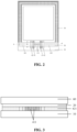
FIG. 2 shows a schematic diagram of a packaging structure according to an embodiment of the present application. -
FIG. 3 shows a cross-sectional schematic diagram at A-A' inFIG. 2 . -
FIG. 4 shows a schematic diagram of a metal extension layer according to an embodiment of the present application. -
FIG. 5 shows a schematic diagram of a metal extension layer according to another embodiment of the present application. - In order to make the purposes, technical means and advantages of the present application more clear, the present application will be further described in detail below with reference to the accompanying drawings. Obviously, the described embodiments are only a part of the embodiments of the present application, and not all of the embodiments of the present application.
- The packaging structure of the present application will be described in more detail below with reference to the accompanying drawings, which illustrates a preferred embodiment of the present application, and it should be understood that those skilled in the art may modify the present application described herein and the advantageous effects of the present application can still be achieved. The present application is described more specifically by a way of an example in the following paragraphs with reference to the accompanying drawings. According to the following instructions and claims, the advantages and characteristics of the present application will be clearer. It should be noted that the accompanying drawings are in a very simplified form and all of the accompanying drawings use inaccurate proportions only to assist conveniently and clearly illustrating the purpose of the embodiments of the present application.
- In the following description, it should be understood that when a layer (or a film or a region or a pattern or a structure) is disposed on a substrate (or a layer or a film or a region or a pad or a pattern), the layer (or the film or the region or the pattern or the structure) may be directly disposed on a surface of the substrate (or the layer or the film or the region or the pad or the pattern), and/or another layer may also be disposed there between. In addition, it should be understood that when a layer is disposed under another layer, the layer may be directly under a surface of another layer, and/or a third layer may also be disposed there between. In addition, whether a layer is disposed on or under another layer can be illustrated by accompanying drawings.
- Referring to
Fig. 1 , the inventor has studied the packaging structure including asubstrate 1, a shape of which is a polygon (e.g., a rectangle); apower supply terminal 4 is disposed on a first side of thesubstrate 1, and ametal layer 3 is disposed on the second side of thesubstrate 1. A packaging layer 2 (e.g., frit) is disposed around the substrate 1(e.g., in a circular pattern) and thepackaging layer 2 is disposed on themetal layer 3 and thepower supply terminal 4, and then another substrate (not shown in theFig.1 ) is packaged together with thesubstrate 1 by thepackaging layer 2. - However, there are some film layers disposed in the
substrate 1 in general, such as signal lines etc. As described above, due to the high temperature and other factors during the packaging process, cracks are generated on the film layer under the packaging layer 2 (e.g., frit), which may result in breakage of the signal lines, thereby may cause an abnormal display. By further studying of the inventor, the inventor found that the cracks are mainly generated at the packaging layer 2 (e.g., frit) and further extending to affect other film layers. - Thus, the present invention proposes a packaging structure, and the packaging structure includes:
- a first substrate, a first side of the first substrate including a power supply terminal;
- a second substrate;
- a metal extension layer, comprising a plurality of first via holes for stress relief, extending from the power supply terminal to both ends of the first side of the first substrate; and,
- a packaging layer, disposed between the first substrate and the second substrate, covering the metal extension layer, and fastening the first substrate and the second substrate, wherein a width of the metal extension layer is same to a width of the packaging layer.
- In order to clearly describe the technical scheme of the present application, preferred embodiments of a packaging structure of a touch screen and a method thereof are provided as follows application. It should be clear that the content of the present application is not limited to the following embodiments, and other improvements made through conventional techniques of those skilled in the art are also within the scope of the present application.
- As shown in
Fig. 2 to Fig. 5 , the packaging structure of the embodiment of the present application includes: - a
first substrate 10, wherein, a first side of thefirst substrate 10 includespower supply terminals - a
second substrate 60; - metal extension layers 411,421 comprising a plurality of first via
holes 50 for stress relief, extending from thepower supply terminal - a
packaging layer 20 covering the metal extension layers 411,421 and fastening thefirst substrate 10 and thesecond substrate 60, - wherein a width of the metal extension layers 411, 421 is same to a width of the
packaging layer 20. - For presentation purposes, the
second substrate 60 is not shown inFig. 2 . - The
first substrate 10 may be, for example, a display substrate. A display structure, for example, an OLED structure etc., is formed on the first substrate 10.The present application does not particularly limit a structure of the display formed on the first substrate. The structure of the display formed on the first substrate may be designed according to actual needs. For example, a conventional driving circuit may also be formed on thefirst substrate 10. A drain electrode of a driving transistor of the driving circuit is electrically connected to a bottom electrode of the OLED by a via hole. The specific structure and the forming method of the driving circuit are well known in prior art and will not be described in detail herein. A passivation layer may also be formed on thefirst substrate 10, used for protecting the driving circuit formed on the first substrate. The passivation layer is preferably made of inorganic material, such as silicon nitride, silicon oxide, aluminum oxide, etc. However it should be understood that the inorganic material (such as silicon nitride, silicon oxide, aluminum oxide, etc.) is only an example of the material of the passivation layer, but the selection range of the material of the passivation layer in the present application is not limited to the above examples, and the material of the passivation layer may be selected in the existing published or commercial materials. - A surrounding region of the display structure may be a driving region, used for applying a voltage to the display structure for example. For example, the
first metal layer 30 shown inFig. 2 is formed in the driving region. - In an embodiment of the present application, a shape of the
first substrate 10 is a polygon, and the power supply terminal is disposed on a first side of the polygon, for example a shape of thefirst substrate 10 is a rectangle and the power supply terminal is disposed on a side of the rectangle. - In a further embodiment, a
first metal layer 30 is disposed on a second side of the polygon, and thepackaging layer 20 is disposed on thefirst metal layer 30. - In a further embodiment, the
first metal layer 30 includes a plurality of third via holes. The third via holes can effectively eliminate stress and reduce the risk of the breakage of signal lines. - In an embodiment, the
second substrate 60 may be a packaging substrate for example. - In an embodiment of the present application, the
power supply terminals Fig. 2 , thepower supply terminals voltage terminals 41 and twocommon ground terminals 42, the two workingvoltage terminals 41 are disposed in the middle of a side of thefirst substrate 10, and the twocommon ground terminals 42 are respectively disposed on both sides of the two workingvoltage terminals 41. - It should be understood that the working
voltage terminal 41 and thecommon ground terminal 42 are inconvenient to contact with each other. Therefore, the metal extension layers 411, 421 extending from the workingvoltage terminal 41 and thecommon ground terminal 42 are inconvenient to contact with each other too. That is, a firstmetal extension layer 411 and a secondmetal extension layer 421 extend respectively from the working voltage terminal (VDD) 41 and the common ground terminal(VSS) 42 to both ends of the side, and a portion of the firstmetal extension layer 411 is not in contact with a portion of thesecond metal 421 extension layer when the portion of the firstmetal extension layer 411 and the portion of the secondmetal extension layer 421 extend face to face respectively from the working voltage terminal and the common ground terminal. - As shown in
Fig.2 , the portion of the firstmetal extension layer 411 and the portion of themetal extension layer 421 may be positively opposite each other, or may be staggered of course. When the portion of themetal extension layer 411 and the portion of themetal extension layer 421 are staggered, the portion of themetal extension layer 411 and the portion of themetal extension layer 421 may have a common overlapping part, and of course, it is better to make the portion of themetal extension layer 411 and the portion of themetal extension layer 421 not contacting with each other. - In a further embodiment, the
metal extension layer 411 and themetal extension layer 421 may be made of one of lithium, magnesium, strontium, aluminum, indium, copper, gold and silver, or may be made of an alloy containing two or more of lithium, magnesium, strontium, aluminum, indium, copper, gold and silver. - In a further embodiment, as shown in
Fig. 2 , the firstmetal extension layer 411 extends from the working voltage terminal (VDD) 41 to both ends of the side and the secondmetal extension layer 421 extends from the common ground terminal (VSS) 42 to both ends of the side, Specifically, for example a shape of thefirst substrate 10 is a rectangular. Thepower supply terminals first substrate 10, the firstmetal extension layer 411 and the secondmetal extension layer 421 extends respectively from the working voltage terminal (VDD) 41 and the common ground terminal (VSS) 42 towards opposite sides on both ends of the side provided with thepower supply terminals packaging layer 20. - Thus, when the
packaging layer 20 is heated for packaging, a heat quantity generated during the pack aging may be better transferred by themetal extension layer 411 and themetal extension layer 421, which contribute to conducting thermal energy, preventing local temperature difference from being too large, and improving the breakage of the signal line. - In the present invention, the metal extension layers (for example the
metal extension layer 411 and/or the metal extension layer 421) include a plurality of first via holes 50. - Referring to
Fig. 4 , a part of themetal extension layer 421 is taken as an example. Themetal extension layer 421 extends from the power supply terminal 42 (specifically the common ground terminal). Themetal extension layer 421 includes the first viaholes 50, and thepower supply terminal 42 may include a plurality of second via holes 50' too. An arrangement of the second via holes 50' in thepower supply terminal 42, may be the same as an arrangement of the first viaholes 50 in themetal extension layer 421, and the second viaholes 50 may be spaced in the whole thepower supply terminal 42. - In a further embodiment, the first via
holes 50 may be evenly spaced or unevenly spaced. For example, a number of the first viaholes 50 is relatively large at a position where the breakage is more likely to occur, and there is no first viaholes 50 or fewer first viaholes 50 at a position where the breakage is less likely to occur. - In a further embodiment, the first via
holes 50 and the second via holes 50' are square holes for example, and have a size (e.g., a side length) of between 50µm and 100µm. - In the present invention, because of the first via
holes 50 comprised in the metal extension layers (for example themetal extension layer 411 and/or the metal extension layer 421), the stress may be effectively eliminated and the risk of the breakage of the signal line may be reduced by the first via holes 50. - In the present invention, a width W2 of the metal extension layer (for example the second extension layer 421) is same to a width W1 of the
packaging layer 20, so that the temperature difference can be effectively reduced, and the thickness uniformity of the film can be improved. - In another embodiment, not forming part of the present invention, the metal extension layers (for example the
metal extension layer 411 and/or the metal extension layer 421) may not include the first via holes 50. As shown inFig. 5 , taking themetal extension layer 421 for an example, a shape of themetal extension layer 421 may be a solid strip. In consideration of stress problems caused by the structure of themetal extension layer 421 without the first viaholes 50, the width of themetal extension layer 421 may be appropriately reduced. For example, the width W3 of themetal extension layer 421 may be 1/4 to 1/3 of the width W1 of thepackaging layer 20. Further, since the crack usually extends from the middle position of thepackaging layer 20, the middle position of thepackaging layer 20 may be regarded as a stress concentration portion. Therefore, themetal extension layer 421 may be disposed in the middle position of thepackaging layer 20, so that the stress can be well dispersed. - It should be understood that the shape and the width of the
metal extension layer 421 are not limited to the above, and the shape of the metal extension layer 421may be a polyline etc. for example, and the shape and the width of themetal extension layer 421 may be adjusted as needed by those skilled in the art. - Obviously, the
metal extension layer 411 may be substantially identical to themetal extension layer 421, and extension directions and extension lengths of themetal extension layer 411 and themetal extension layer 421 may be different. - The
packaging layer 20 is configured to fix (e.g., by a method of bonding) thefirst substrate 10 and thesecond substrate 60 and formed a packaging strip, and thepackaging layer 20 may generally be the frit including fine glass particles. The glass particles include one material or more materials of the following materials: magnesium oxide (MgO), calcium oxide (CaO), barium oxide (BaO), lithium oxide (Li2O), sodium oxide (Na2O), potassium oxide (K2O), boron oxide (B2O3), vanadium oxide (V2O5), zinc oxide (ZnO), tellurium oxide (TeO2), alumina (Al2O3), silicon dioxide (SiO2), lead oxide (PbO), tin oxide (SnO), phosphorus oxide (P2O5), ruthenium oxide (Ru2O), ruthenium oxide (Rb2O), ruthenium oxide (Rh2O), iron oxide (Fe2O3), copper oxide (CuO), titanium oxide (TiO2), tungsten oxide (WO3), bismuth oxide (Bi2O3), antimony oxide (Sb2O3), lead-borate glass, tin-phosphate glass, vanadate glass, borosilicate, etc. - In order to ensure reliability of sealing, the frit wraps around the
first substrate 10 for a whole circle, and a position covered by the frit is generally referred to as a packaging region. - Moreover, by means of the metal extension layer, which is mentioned above, (i.e. including the first via
holes 50 or a width of the metal extension layer being 1/4 to 1/3 of the width of the packaging layer 20) thepackaging layer 20 is facilitated to be in contact with a dielectric layer under the metal extension layer, thereby packaging effect can be improved. - In summary, the packaging structure, provided by the present invention, includes: a first substrate, a first side of the first substrate including a power supply terminal; a second substrate; a metal extension layer comprising a plurality of first via holes for stress relief, extending from the power supply terminal to both ends of the first side of the first substrate; and a packaging layer disposed between the first substrate and the second substrate, covering the metal extension layer and fastening the first substrate and the second substrate, wherein a width of the metal extension layer is same to a width of the packaging layer.
- Thus through extended filling of metal materials, conducting of thermal energy and the breakage of the signal line can be improved.
- Further, the uniformity of the thickness of the film may be improved by a design of the width of the metal extension layer being same to the width of the packaging layer.
- Further, by the first via
holes 50 spaced in the metal extension layer, the stress can be effectively eliminated and the risk of the breakage of the signal line can be reduced. - An OLED display device, including the packaging structure described above, is also provided in the present invention.
Claims (11)
- A packaging structure, comprising:a first substrate (10), a first side of the first substrate (10) comprising a power supply terminal (41,42);a second substrate (60);a metal extension layer (411, 421), extending from the power supply terminal (41, 42) to both ends of the first side of the first substrate (10); and,a packaging layer (20), disposed between the first substrate (10) and the second substrate (60), covering the metal extension layer (411, 412), and fastening the first substrate (10) and the second substrate (60);characterized in that the metal extension layer (411, 421)comprises a plurality of first via holes (50) for stress relief, and in that a width of the metal extension layer (411,421) is same to a width of the packaging layer (20).
- The packaging structure of claim 1, wherein the second substrate (60) is a packaging cover.
- The packaging structure of claim 1 or 2, wherein the first via holes (50) are spaced evenly.
- The packaging structure of any one of the previous claims, wherein the power supply terminal (41, 42) compromises a plurality of second via holes (50').
- The packaging structure of claim 4, wherein each of the first via holes (50) is in a shape of square, and/or each of the second via holes (50') is in a shape of square.
- The packaging structure of any one of the previous claims, wherein the power supply terminal comprises a working voltage terminal (41) and a common ground terminal (42).
- The packaging structure of claim 6, wherein the metal extension layer comprises a first metal extension layer (411) extending from the working voltage terminal (41) and a second metal extension layer (421) extending the common ground terminal (42) to both ends of the first side of the substrate, and a portion of the first metal extension layer (411) and a portion of the second metal extension layer (421) extend toward each other and not in contact with each other.
- The packaging structure of any one of the previous claims, wherein a shape of the first substrate (10) is a polygon and the power supply terminal is disposed at a side of the polygon.
- The packaging structure of claim 8, further comprising:
a first metal layer (30), disposed on a second side of the polygon; wherein the packaging layer (20) is disposed on the first metal layer (10). - The packaging structure of claim 9, wherein the first metal layer (10) comprises a plurality of third via holes.
- An OLED display device, comprising the packaging structure of any one of claims 1 to 10.
Applications Claiming Priority (2)
| Application Number | Priority Date | Filing Date | Title |
|---|---|---|---|
| CN201820093096.4U CN208014747U (en) | 2018-01-19 | 2018-01-19 | Encapsulating structure |
| PCT/CN2018/107599 WO2019140948A1 (en) | 2018-01-19 | 2018-09-26 | Encapsulation structure |
Publications (3)
| Publication Number | Publication Date |
|---|---|
| EP3641000A1 EP3641000A1 (en) | 2020-04-22 |
| EP3641000A4 EP3641000A4 (en) | 2020-11-18 |
| EP3641000B1 true EP3641000B1 (en) | 2024-02-14 |
Family
ID=63883165
Family Applications (1)
| Application Number | Title | Priority Date | Filing Date |
|---|---|---|---|
| EP18901014.3A Active EP3641000B1 (en) | 2018-01-19 | 2018-09-26 | Encapsulation structure |
Country Status (6)
| Country | Link |
|---|---|
| US (1) | US10756296B2 (en) |
| EP (1) | EP3641000B1 (en) |
| JP (1) | JP7261796B2 (en) |
| KR (1) | KR102362044B1 (en) |
| CN (1) | CN208014747U (en) |
| WO (1) | WO2019140948A1 (en) |
Families Citing this family (3)
| Publication number | Priority date | Publication date | Assignee | Title |
|---|---|---|---|---|
| US11477904B2 (en) * | 2020-03-02 | 2022-10-18 | Te Connectivity Solutions Gmbh | Electronic assembly including cable modules |
| KR102864432B1 (en) * | 2021-07-14 | 2025-09-25 | 삼성디스플레이 주식회사 | Display device |
| CN113629079B (en) * | 2021-08-30 | 2025-08-19 | 京东方科技集团股份有限公司 | Display substrate, manufacturing method thereof and display device |
Citations (1)
| Publication number | Priority date | Publication date | Assignee | Title |
|---|---|---|---|---|
| EP1814181A2 (en) * | 2006-01-26 | 2007-08-01 | Samsung SDI Co., Ltd. | Organic light emitting display device |
Family Cites Families (25)
| Publication number | Priority date | Publication date | Assignee | Title |
|---|---|---|---|---|
| US6911733B2 (en) * | 2002-02-28 | 2005-06-28 | Hitachi, Ltd. | Semiconductor device and electronic device |
| JP2004061707A (en) * | 2002-07-26 | 2004-02-26 | Seiko Epson Corp | Liquid crystal devices and electronic equipment |
| KR100592273B1 (en) * | 2004-05-20 | 2006-06-22 | 삼성에스디아이 주식회사 | Flat panel display device |
| US20070271808A9 (en) * | 2004-09-21 | 2007-11-29 | Eastman Kodak Company | Lewis acid organometallic desiccant |
| KR100700653B1 (en) * | 2005-02-03 | 2007-03-27 | 삼성에스디아이 주식회사 | Organic light emitting display device |
| JP4774787B2 (en) * | 2005-03-31 | 2011-09-14 | Tdk株式会社 | Display device |
| KR100720143B1 (en) * | 2005-12-13 | 2007-05-18 | 삼성전자주식회사 | Display device |
| US20070153354A1 (en) * | 2005-12-22 | 2007-07-05 | Solbeam, Inc. | Minimizing lensing in electro-optic prisms |
| JP4860530B2 (en) * | 2006-04-04 | 2012-01-25 | コイズミ照明株式会社 | EL light source |
| KR100722118B1 (en) * | 2006-09-04 | 2007-05-25 | 삼성에스디아이 주식회사 | Organic light emitting display device |
| KR20080069032A (en) * | 2007-01-22 | 2008-07-25 | 삼성전자주식회사 | Display device |
| KR20120129283A (en) * | 2011-05-19 | 2012-11-28 | 삼성디스플레이 주식회사 | Organic light emitting diode display and method for manufacturing the same |
| TWI471661B (en) * | 2011-06-29 | 2015-02-01 | Innolux Corp | System for display images |
| TW201411904A (en) * | 2012-09-10 | 2014-03-16 | Ultimate Image Corp | Organic light emitting diode planar lighting device |
| KR102160829B1 (en) * | 2012-11-02 | 2020-09-28 | 가부시키가이샤 한도오따이 에네루기 켄큐쇼 | Sealed body and method for manufacturing the same |
| JP5982060B2 (en) * | 2013-04-25 | 2016-08-31 | パナソニック株式会社 | Passive matrix drive display and tiling display |
| KR102135882B1 (en) * | 2013-07-22 | 2020-07-22 | 삼성디스플레이 주식회사 | Organic light emitting display device |
| CN104157792A (en) * | 2014-08-08 | 2014-11-19 | 上海和辉光电有限公司 | OLED (organic light emitting diode) packaging structure and method |
| CN104183686B (en) * | 2014-09-09 | 2018-02-02 | 厦门市三安光电科技有限公司 | LED device and preparation method thereof |
| CN104882566B (en) * | 2015-05-21 | 2017-12-22 | 京东方科技集团股份有限公司 | A kind of package structure for LED and method for packing |
| WO2017033630A1 (en) * | 2015-08-26 | 2017-03-02 | 株式会社カネカ | Planar light emitting device |
| KR102439308B1 (en) * | 2015-10-06 | 2022-09-02 | 삼성디스플레이 주식회사 | display |
| CN106816546B (en) | 2015-11-30 | 2019-08-23 | 上海和辉光电有限公司 | A kind of OLED array and OLED display device |
| KR102725327B1 (en) * | 2016-12-30 | 2024-11-01 | 엘지디스플레이 주식회사 | Antenna Integrated Polarizer and Flexible Display Device Using the Same |
| CN108493226B (en) * | 2018-05-14 | 2021-04-30 | 上海天马有机发光显示技术有限公司 | Electronic equipment, display panel and preparation method thereof |
-
2018
- 2018-01-19 CN CN201820093096.4U patent/CN208014747U/en active Active
- 2018-09-26 KR KR1020207001024A patent/KR102362044B1/en active Active
- 2018-09-26 EP EP18901014.3A patent/EP3641000B1/en active Active
- 2018-09-26 JP JP2020523482A patent/JP7261796B2/en active Active
- 2018-09-26 WO PCT/CN2018/107599 patent/WO2019140948A1/en not_active Ceased
-
2019
- 2019-03-05 US US16/293,426 patent/US10756296B2/en active Active
Patent Citations (1)
| Publication number | Priority date | Publication date | Assignee | Title |
|---|---|---|---|---|
| EP1814181A2 (en) * | 2006-01-26 | 2007-08-01 | Samsung SDI Co., Ltd. | Organic light emitting display device |
Also Published As
| Publication number | Publication date |
|---|---|
| CN208014747U (en) | 2018-10-26 |
| EP3641000A1 (en) | 2020-04-22 |
| JP2020527289A (en) | 2020-09-03 |
| EP3641000A4 (en) | 2020-11-18 |
| KR102362044B1 (en) | 2022-02-14 |
| JP7261796B2 (en) | 2023-04-20 |
| KR20200011048A (en) | 2020-01-31 |
| WO2019140948A1 (en) | 2019-07-25 |
| US20190207143A1 (en) | 2019-07-04 |
| US10756296B2 (en) | 2020-08-25 |
Similar Documents
| Publication | Publication Date | Title |
|---|---|---|
| CN109119447B (en) | A display panel and display device | |
| CN110047883B (en) | Organic light emitting display device and method of manufacturing organic light emitting display device | |
| TWI333286B (en) | Organic electroluminescence display device and manufacturing method thereof | |
| TWI461094B (en) | Organic light emitting display device and manufacturing method | |
| CN100511755C (en) | Organic light emitting display and method of manufacturing the same | |
| US9660007B2 (en) | Display device and method of manufacturing display device | |
| TWI323521B (en) | Organic electroluminescence display device and manufacturing method thereof | |
| RU2738785C1 (en) | Display panel, a display device, a method of detecting a crack in a sealing layer of a display panel and a method of making a display panel | |
| US8742526B2 (en) | Photoelectric conversion device | |
| CN101009316B (en) | Flat panel display device and method of making the same | |
| CN101009310A (en) | Organic light emitting display and method of fabricating the same | |
| US10756296B2 (en) | Packaging structure | |
| KR102439308B1 (en) | display | |
| CN100452936C (en) | Display panel and method for manufacturing display panel | |
| CN108598284B (en) | Display panel, display panel preparation method and display device | |
| KR20120083697A (en) | Flat panel display device and method of manufacturing thereof | |
| CN110098228A (en) | A kind of display panel and display device | |
| KR102426120B1 (en) | Mirror display device | |
| KR100683407B1 (en) | Display device and manufacturing method thereof | |
| EP3427300B1 (en) | Encapsulation structure and display apparatus | |
| KR100703457B1 (en) | Organic electroluminescent display and manufacturing method thereof | |
| CN110071223A (en) | A kind of OLED encapsulating structure and OLED encapsulation method | |
| TWM572076U (en) | Package structure | |
| KR100698688B1 (en) | Organic light emitting display device and manufacturing method thereof | |
| KR100707597B1 (en) | Organic light emitting display device and manufacturing method thereof |
Legal Events
| Date | Code | Title | Description |
|---|---|---|---|
| STAA | Information on the status of an ep patent application or granted ep patent |
Free format text: STATUS: THE INTERNATIONAL PUBLICATION HAS BEEN MADE |
|
| PUAI | Public reference made under article 153(3) epc to a published international application that has entered the european phase |
Free format text: ORIGINAL CODE: 0009012 |
|
| STAA | Information on the status of an ep patent application or granted ep patent |
Free format text: STATUS: REQUEST FOR EXAMINATION WAS MADE |
|
| 17P | Request for examination filed |
Effective date: 20200116 |
|
| AK | Designated contracting states |
Kind code of ref document: A1 Designated state(s): AL AT BE BG CH CY CZ DE DK EE ES FI FR GB GR HR HU IE IS IT LI LT LU LV MC MK MT NL NO PL PT RO RS SE SI SK SM TR |
|
| AX | Request for extension of the european patent |
Extension state: BA ME |
|
| A4 | Supplementary search report drawn up and despatched |
Effective date: 20201016 |
|
| RIC1 | Information provided on ipc code assigned before grant |
Ipc: H01L 51/52 20060101AFI20201012BHEP Ipc: H01L 27/32 20060101ALI20201012BHEP |
|
| DAV | Request for validation of the european patent (deleted) | ||
| DAX | Request for extension of the european patent (deleted) | ||
| STAA | Information on the status of an ep patent application or granted ep patent |
Free format text: STATUS: EXAMINATION IS IN PROGRESS |
|
| 17Q | First examination report despatched |
Effective date: 20220325 |
|
| 17Q | First examination report despatched |
Effective date: 20220405 |
|
| REG | Reference to a national code |
Ref country code: DE Ref legal event code: R079 Free format text: PREVIOUS MAIN CLASS: H01L0051520000 Ipc: H10K0059800000 Ref document number: 602018065373 Country of ref document: DE |
|
| GRAP | Despatch of communication of intention to grant a patent |
Free format text: ORIGINAL CODE: EPIDOSNIGR1 |
|
| STAA | Information on the status of an ep patent application or granted ep patent |
Free format text: STATUS: GRANT OF PATENT IS INTENDED |
|
| RIC1 | Information provided on ipc code assigned before grant |
Ipc: H10K 50/84 20230101ALI20231115BHEP Ipc: H10K 59/131 20230101ALI20231115BHEP Ipc: H10K 59/80 20230101AFI20231115BHEP |
|
| INTG | Intention to grant announced |
Effective date: 20231130 |
|
| GRAS | Grant fee paid |
Free format text: ORIGINAL CODE: EPIDOSNIGR3 |
|
| GRAA | (expected) grant |
Free format text: ORIGINAL CODE: 0009210 |
|
| STAA | Information on the status of an ep patent application or granted ep patent |
Free format text: STATUS: THE PATENT HAS BEEN GRANTED |
|
| AK | Designated contracting states |
Kind code of ref document: B1 Designated state(s): AL AT BE BG CH CY CZ DE DK EE ES FI FR GB GR HR HU IE IS IT LI LT LU LV MC MK MT NL NO PL PT RO RS SE SI SK SM TR |
|
| REG | Reference to a national code |
Ref country code: GB Ref legal event code: FG4D |
|
| REG | Reference to a national code |
Ref country code: CH Ref legal event code: EP |
|
| REG | Reference to a national code |
Ref country code: DE Ref legal event code: R096 Ref document number: 602018065373 Country of ref document: DE |
|
| REG | Reference to a national code |
Ref country code: IE Ref legal event code: FG4D |
|
| REG | Reference to a national code |
Ref country code: LT Ref legal event code: MG9D |
|
| REG | Reference to a national code |
Ref country code: NL Ref legal event code: MP Effective date: 20240214 |
|
| PG25 | Lapsed in a contracting state [announced via postgrant information from national office to epo] |
Ref country code: IS Free format text: LAPSE BECAUSE OF FAILURE TO SUBMIT A TRANSLATION OF THE DESCRIPTION OR TO PAY THE FEE WITHIN THE PRESCRIBED TIME-LIMIT Effective date: 20240614 |
|
| PG25 | Lapsed in a contracting state [announced via postgrant information from national office to epo] |
Ref country code: LT Free format text: LAPSE BECAUSE OF FAILURE TO SUBMIT A TRANSLATION OF THE DESCRIPTION OR TO PAY THE FEE WITHIN THE PRESCRIBED TIME-LIMIT Effective date: 20240214 |
|
| PG25 | Lapsed in a contracting state [announced via postgrant information from national office to epo] |
Ref country code: GR Free format text: LAPSE BECAUSE OF FAILURE TO SUBMIT A TRANSLATION OF THE DESCRIPTION OR TO PAY THE FEE WITHIN THE PRESCRIBED TIME-LIMIT Effective date: 20240515 |
|
| REG | Reference to a national code |
Ref country code: AT Ref legal event code: MK05 Ref document number: 1658209 Country of ref document: AT Kind code of ref document: T Effective date: 20240214 |
|
| PG25 | Lapsed in a contracting state [announced via postgrant information from national office to epo] |
Ref country code: NL Free format text: LAPSE BECAUSE OF FAILURE TO SUBMIT A TRANSLATION OF THE DESCRIPTION OR TO PAY THE FEE WITHIN THE PRESCRIBED TIME-LIMIT Effective date: 20240214 Ref country code: HR Free format text: LAPSE BECAUSE OF FAILURE TO SUBMIT A TRANSLATION OF THE DESCRIPTION OR TO PAY THE FEE WITHIN THE PRESCRIBED TIME-LIMIT Effective date: 20240214 Ref country code: RS Free format text: LAPSE BECAUSE OF FAILURE TO SUBMIT A TRANSLATION OF THE DESCRIPTION OR TO PAY THE FEE WITHIN THE PRESCRIBED TIME-LIMIT Effective date: 20240514 |
|
| PG25 | Lapsed in a contracting state [announced via postgrant information from national office to epo] |
Ref country code: ES Free format text: LAPSE BECAUSE OF FAILURE TO SUBMIT A TRANSLATION OF THE DESCRIPTION OR TO PAY THE FEE WITHIN THE PRESCRIBED TIME-LIMIT Effective date: 20240214 |
|
| PG25 | Lapsed in a contracting state [announced via postgrant information from national office to epo] |
Ref country code: AT Free format text: LAPSE BECAUSE OF FAILURE TO SUBMIT A TRANSLATION OF THE DESCRIPTION OR TO PAY THE FEE WITHIN THE PRESCRIBED TIME-LIMIT Effective date: 20240214 |
|
| PG25 | Lapsed in a contracting state [announced via postgrant information from national office to epo] |
Ref country code: RS Free format text: LAPSE BECAUSE OF FAILURE TO SUBMIT A TRANSLATION OF THE DESCRIPTION OR TO PAY THE FEE WITHIN THE PRESCRIBED TIME-LIMIT Effective date: 20240514 Ref country code: NO Free format text: LAPSE BECAUSE OF FAILURE TO SUBMIT A TRANSLATION OF THE DESCRIPTION OR TO PAY THE FEE WITHIN THE PRESCRIBED TIME-LIMIT Effective date: 20240514 Ref country code: NL Free format text: LAPSE BECAUSE OF FAILURE TO SUBMIT A TRANSLATION OF THE DESCRIPTION OR TO PAY THE FEE WITHIN THE PRESCRIBED TIME-LIMIT Effective date: 20240214 Ref country code: LT Free format text: LAPSE BECAUSE OF FAILURE TO SUBMIT A TRANSLATION OF THE DESCRIPTION OR TO PAY THE FEE WITHIN THE PRESCRIBED TIME-LIMIT Effective date: 20240214 Ref country code: IS Free format text: LAPSE BECAUSE OF FAILURE TO SUBMIT A TRANSLATION OF THE DESCRIPTION OR TO PAY THE FEE WITHIN THE PRESCRIBED TIME-LIMIT Effective date: 20240614 Ref country code: HR Free format text: LAPSE BECAUSE OF FAILURE TO SUBMIT A TRANSLATION OF THE DESCRIPTION OR TO PAY THE FEE WITHIN THE PRESCRIBED TIME-LIMIT Effective date: 20240214 Ref country code: GR Free format text: LAPSE BECAUSE OF FAILURE TO SUBMIT A TRANSLATION OF THE DESCRIPTION OR TO PAY THE FEE WITHIN THE PRESCRIBED TIME-LIMIT Effective date: 20240515 Ref country code: FI Free format text: LAPSE BECAUSE OF FAILURE TO SUBMIT A TRANSLATION OF THE DESCRIPTION OR TO PAY THE FEE WITHIN THE PRESCRIBED TIME-LIMIT Effective date: 20240214 Ref country code: ES Free format text: LAPSE BECAUSE OF FAILURE TO SUBMIT A TRANSLATION OF THE DESCRIPTION OR TO PAY THE FEE WITHIN THE PRESCRIBED TIME-LIMIT Effective date: 20240214 Ref country code: BG Free format text: LAPSE BECAUSE OF FAILURE TO SUBMIT A TRANSLATION OF THE DESCRIPTION OR TO PAY THE FEE WITHIN THE PRESCRIBED TIME-LIMIT Effective date: 20240214 Ref country code: AT Free format text: LAPSE BECAUSE OF FAILURE TO SUBMIT A TRANSLATION OF THE DESCRIPTION OR TO PAY THE FEE WITHIN THE PRESCRIBED TIME-LIMIT Effective date: 20240214 |
|
| PG25 | Lapsed in a contracting state [announced via postgrant information from national office to epo] |
Ref country code: PL Free format text: LAPSE BECAUSE OF FAILURE TO SUBMIT A TRANSLATION OF THE DESCRIPTION OR TO PAY THE FEE WITHIN THE PRESCRIBED TIME-LIMIT Effective date: 20240214 Ref country code: PT Free format text: LAPSE BECAUSE OF FAILURE TO SUBMIT A TRANSLATION OF THE DESCRIPTION OR TO PAY THE FEE WITHIN THE PRESCRIBED TIME-LIMIT Effective date: 20240614 |
|
| PG25 | Lapsed in a contracting state [announced via postgrant information from national office to epo] |
Ref country code: SE Free format text: LAPSE BECAUSE OF FAILURE TO SUBMIT A TRANSLATION OF THE DESCRIPTION OR TO PAY THE FEE WITHIN THE PRESCRIBED TIME-LIMIT Effective date: 20240214 Ref country code: PT Free format text: LAPSE BECAUSE OF FAILURE TO SUBMIT A TRANSLATION OF THE DESCRIPTION OR TO PAY THE FEE WITHIN THE PRESCRIBED TIME-LIMIT Effective date: 20240614 Ref country code: PL Free format text: LAPSE BECAUSE OF FAILURE TO SUBMIT A TRANSLATION OF THE DESCRIPTION OR TO PAY THE FEE WITHIN THE PRESCRIBED TIME-LIMIT Effective date: 20240214 Ref country code: LV Free format text: LAPSE BECAUSE OF FAILURE TO SUBMIT A TRANSLATION OF THE DESCRIPTION OR TO PAY THE FEE WITHIN THE PRESCRIBED TIME-LIMIT Effective date: 20240214 |
|
| PG25 | Lapsed in a contracting state [announced via postgrant information from national office to epo] |
Ref country code: DK Free format text: LAPSE BECAUSE OF FAILURE TO SUBMIT A TRANSLATION OF THE DESCRIPTION OR TO PAY THE FEE WITHIN THE PRESCRIBED TIME-LIMIT Effective date: 20240214 |
|
| PG25 | Lapsed in a contracting state [announced via postgrant information from national office to epo] |
Ref country code: SM Free format text: LAPSE BECAUSE OF FAILURE TO SUBMIT A TRANSLATION OF THE DESCRIPTION OR TO PAY THE FEE WITHIN THE PRESCRIBED TIME-LIMIT Effective date: 20240214 |
|
| PG25 | Lapsed in a contracting state [announced via postgrant information from national office to epo] |
Ref country code: CZ Free format text: LAPSE BECAUSE OF FAILURE TO SUBMIT A TRANSLATION OF THE DESCRIPTION OR TO PAY THE FEE WITHIN THE PRESCRIBED TIME-LIMIT Effective date: 20240214 Ref country code: EE Free format text: LAPSE BECAUSE OF FAILURE TO SUBMIT A TRANSLATION OF THE DESCRIPTION OR TO PAY THE FEE WITHIN THE PRESCRIBED TIME-LIMIT Effective date: 20240214 |
|
| PG25 | Lapsed in a contracting state [announced via postgrant information from national office to epo] |
Ref country code: SK Free format text: LAPSE BECAUSE OF FAILURE TO SUBMIT A TRANSLATION OF THE DESCRIPTION OR TO PAY THE FEE WITHIN THE PRESCRIBED TIME-LIMIT Effective date: 20240214 |
|
| PG25 | Lapsed in a contracting state [announced via postgrant information from national office to epo] |
Ref country code: SM Free format text: LAPSE BECAUSE OF FAILURE TO SUBMIT A TRANSLATION OF THE DESCRIPTION OR TO PAY THE FEE WITHIN THE PRESCRIBED TIME-LIMIT Effective date: 20240214 Ref country code: SK Free format text: LAPSE BECAUSE OF FAILURE TO SUBMIT A TRANSLATION OF THE DESCRIPTION OR TO PAY THE FEE WITHIN THE PRESCRIBED TIME-LIMIT Effective date: 20240214 Ref country code: RO Free format text: LAPSE BECAUSE OF FAILURE TO SUBMIT A TRANSLATION OF THE DESCRIPTION OR TO PAY THE FEE WITHIN THE PRESCRIBED TIME-LIMIT Effective date: 20240214 Ref country code: EE Free format text: LAPSE BECAUSE OF FAILURE TO SUBMIT A TRANSLATION OF THE DESCRIPTION OR TO PAY THE FEE WITHIN THE PRESCRIBED TIME-LIMIT Effective date: 20240214 Ref country code: DK Free format text: LAPSE BECAUSE OF FAILURE TO SUBMIT A TRANSLATION OF THE DESCRIPTION OR TO PAY THE FEE WITHIN THE PRESCRIBED TIME-LIMIT Effective date: 20240214 Ref country code: CZ Free format text: LAPSE BECAUSE OF FAILURE TO SUBMIT A TRANSLATION OF THE DESCRIPTION OR TO PAY THE FEE WITHIN THE PRESCRIBED TIME-LIMIT Effective date: 20240214 |
|
| REG | Reference to a national code |
Ref country code: DE Ref legal event code: R097 Ref document number: 602018065373 Country of ref document: DE |
|
| PG25 | Lapsed in a contracting state [announced via postgrant information from national office to epo] |
Ref country code: IT Free format text: LAPSE BECAUSE OF FAILURE TO SUBMIT A TRANSLATION OF THE DESCRIPTION OR TO PAY THE FEE WITHIN THE PRESCRIBED TIME-LIMIT Effective date: 20240214 |
|
| PLBE | No opposition filed within time limit |
Free format text: ORIGINAL CODE: 0009261 |
|
| STAA | Information on the status of an ep patent application or granted ep patent |
Free format text: STATUS: NO OPPOSITION FILED WITHIN TIME LIMIT |
|
| PG25 | Lapsed in a contracting state [announced via postgrant information from national office to epo] |
Ref country code: IT Free format text: LAPSE BECAUSE OF FAILURE TO SUBMIT A TRANSLATION OF THE DESCRIPTION OR TO PAY THE FEE WITHIN THE PRESCRIBED TIME-LIMIT Effective date: 20240214 |
|
| 26N | No opposition filed |
Effective date: 20241115 |
|
| PG25 | Lapsed in a contracting state [announced via postgrant information from national office to epo] |
Ref country code: SI Free format text: LAPSE BECAUSE OF FAILURE TO SUBMIT A TRANSLATION OF THE DESCRIPTION OR TO PAY THE FEE WITHIN THE PRESCRIBED TIME-LIMIT Effective date: 20240214 Ref country code: MC Free format text: LAPSE BECAUSE OF FAILURE TO SUBMIT A TRANSLATION OF THE DESCRIPTION OR TO PAY THE FEE WITHIN THE PRESCRIBED TIME-LIMIT Effective date: 20240214 |
|
| REG | Reference to a national code |
Ref country code: CH Ref legal event code: PL |
|
| PG25 | Lapsed in a contracting state [announced via postgrant information from national office to epo] |
Ref country code: LU Free format text: LAPSE BECAUSE OF NON-PAYMENT OF DUE FEES Effective date: 20240926 |
|
| REG | Reference to a national code |
Ref country code: BE Ref legal event code: MM Effective date: 20240930 |
|
| PG25 | Lapsed in a contracting state [announced via postgrant information from national office to epo] |
Ref country code: BE Free format text: LAPSE BECAUSE OF NON-PAYMENT OF DUE FEES Effective date: 20240930 |
|
| PG25 | Lapsed in a contracting state [announced via postgrant information from national office to epo] |
Ref country code: CH Free format text: LAPSE BECAUSE OF NON-PAYMENT OF DUE FEES Effective date: 20240930 |
|
| PG25 | Lapsed in a contracting state [announced via postgrant information from national office to epo] |
Ref country code: IE Free format text: LAPSE BECAUSE OF NON-PAYMENT OF DUE FEES Effective date: 20240926 |
|
| PGFP | Annual fee paid to national office [announced via postgrant information from national office to epo] |
Ref country code: DE Payment date: 20250916 Year of fee payment: 8 |
|
| PGFP | Annual fee paid to national office [announced via postgrant information from national office to epo] |
Ref country code: GB Payment date: 20250919 Year of fee payment: 8 |
|
| PGFP | Annual fee paid to national office [announced via postgrant information from national office to epo] |
Ref country code: FR Payment date: 20250929 Year of fee payment: 8 |
|
| PG25 | Lapsed in a contracting state [announced via postgrant information from national office to epo] |
Ref country code: CY Free format text: LAPSE BECAUSE OF FAILURE TO SUBMIT A TRANSLATION OF THE DESCRIPTION OR TO PAY THE FEE WITHIN THE PRESCRIBED TIME-LIMIT; INVALID AB INITIO Effective date: 20180926 |
|
| PG25 | Lapsed in a contracting state [announced via postgrant information from national office to epo] |
Ref country code: HU Free format text: LAPSE BECAUSE OF FAILURE TO SUBMIT A TRANSLATION OF THE DESCRIPTION OR TO PAY THE FEE WITHIN THE PRESCRIBED TIME-LIMIT; INVALID AB INITIO Effective date: 20180926 |