EP3637515A1 - Secondary battery and electrode member thereof - Google Patents
Secondary battery and electrode member thereof Download PDFInfo
- Publication number
- EP3637515A1 EP3637515A1 EP19153878.4A EP19153878A EP3637515A1 EP 3637515 A1 EP3637515 A1 EP 3637515A1 EP 19153878 A EP19153878 A EP 19153878A EP 3637515 A1 EP3637515 A1 EP 3637515A1
- Authority
- EP
- European Patent Office
- Prior art keywords
- conducting layer
- electrode member
- insulating substrate
- stripe
- layer
- Prior art date
- Legal status (The legal status is an assumption and is not a legal conclusion. Google has not performed a legal analysis and makes no representation as to the accuracy of the status listed.)
- Granted
Links
- 239000000758 substrate Substances 0.000 claims abstract description 76
- 239000011149 active material Substances 0.000 claims abstract description 48
- 230000003578 releasing effect Effects 0.000 abstract description 7
- 238000005096 rolling process Methods 0.000 description 20
- 238000000034 method Methods 0.000 description 12
- 239000002002 slurry Substances 0.000 description 12
- 230000000694 effects Effects 0.000 description 8
- OKTJSMMVPCPJKN-UHFFFAOYSA-N Carbon Chemical compound [C] OKTJSMMVPCPJKN-UHFFFAOYSA-N 0.000 description 7
- 229910052751 metal Inorganic materials 0.000 description 5
- 239000002184 metal Substances 0.000 description 5
- 229910052782 aluminium Inorganic materials 0.000 description 4
- XAGFODPZIPBFFR-UHFFFAOYSA-N aluminium Chemical compound [Al] XAGFODPZIPBFFR-UHFFFAOYSA-N 0.000 description 4
- 239000011230 binding agent Substances 0.000 description 4
- 239000004020 conductor Substances 0.000 description 4
- 230000003247 decreasing effect Effects 0.000 description 4
- 239000011810 insulating material Substances 0.000 description 4
- 229920000139 polyethylene terephthalate Polymers 0.000 description 4
- 239000005020 polyethylene terephthalate Substances 0.000 description 4
- 238000007740 vapor deposition Methods 0.000 description 4
- 238000004804 winding Methods 0.000 description 4
- 229910052799 carbon Inorganic materials 0.000 description 3
- 238000000576 coating method Methods 0.000 description 3
- 238000007772 electroless plating Methods 0.000 description 3
- 239000000463 material Substances 0.000 description 3
- 239000007769 metal material Substances 0.000 description 3
- -1 polyethylene terephthalate Polymers 0.000 description 3
- 239000002904 solvent Substances 0.000 description 3
- WHXSMMKQMYFTQS-UHFFFAOYSA-N Lithium Chemical compound [Li] WHXSMMKQMYFTQS-UHFFFAOYSA-N 0.000 description 2
- PXHVJJICTQNCMI-UHFFFAOYSA-N Nickel Chemical compound [Ni] PXHVJJICTQNCMI-UHFFFAOYSA-N 0.000 description 2
- 239000004743 Polypropylene Substances 0.000 description 2
- 239000011248 coating agent Substances 0.000 description 2
- 239000000306 component Substances 0.000 description 2
- 238000005520 cutting process Methods 0.000 description 2
- 238000009826 distribution Methods 0.000 description 2
- 239000011888 foil Substances 0.000 description 2
- 229910052744 lithium Inorganic materials 0.000 description 2
- 230000002093 peripheral effect Effects 0.000 description 2
- 230000010287 polarization Effects 0.000 description 2
- 229910000838 Al alloy Inorganic materials 0.000 description 1
- RYGMFSIKBFXOCR-UHFFFAOYSA-N Copper Chemical compound [Cu] RYGMFSIKBFXOCR-UHFFFAOYSA-N 0.000 description 1
- 229910000881 Cu alloy Inorganic materials 0.000 description 1
- BQCADISMDOOEFD-UHFFFAOYSA-N Silver Chemical compound [Ag] BQCADISMDOOEFD-UHFFFAOYSA-N 0.000 description 1
- RTAQQCXQSZGOHL-UHFFFAOYSA-N Titanium Chemical compound [Ti] RTAQQCXQSZGOHL-UHFFFAOYSA-N 0.000 description 1
- 229910001093 Zr alloy Inorganic materials 0.000 description 1
- ZGUQGPFMMTZGBQ-UHFFFAOYSA-N [Al].[Al].[Zr] Chemical compound [Al].[Al].[Zr] ZGUQGPFMMTZGBQ-UHFFFAOYSA-N 0.000 description 1
- 239000004411 aluminium Substances 0.000 description 1
- 230000009286 beneficial effect Effects 0.000 description 1
- 230000005540 biological transmission Effects 0.000 description 1
- 239000006229 carbon black Substances 0.000 description 1
- 239000002041 carbon nanotube Substances 0.000 description 1
- 229910021393 carbon nanotube Inorganic materials 0.000 description 1
- 239000002131 composite material Substances 0.000 description 1
- 239000012141 concentrate Substances 0.000 description 1
- 239000006258 conductive agent Substances 0.000 description 1
- 229910052802 copper Inorganic materials 0.000 description 1
- 239000010949 copper Substances 0.000 description 1
- YOCUPQPZWBBYIX-UHFFFAOYSA-N copper nickel Chemical compound [Ni].[Cu] YOCUPQPZWBBYIX-UHFFFAOYSA-N 0.000 description 1
- 239000008358 core component Substances 0.000 description 1
- 238000000151 deposition Methods 0.000 description 1
- 230000008021 deposition Effects 0.000 description 1
- 239000003792 electrolyte Substances 0.000 description 1
- 229910021389 graphene Inorganic materials 0.000 description 1
- 229910002804 graphite Inorganic materials 0.000 description 1
- 239000010439 graphite Substances 0.000 description 1
- FAHBNUUHRFUEAI-UHFFFAOYSA-M hydroxidooxidoaluminium Chemical compound O[Al]=O FAHBNUUHRFUEAI-UHFFFAOYSA-M 0.000 description 1
- GELKBWJHTRAYNV-UHFFFAOYSA-K lithium iron phosphate Chemical compound [Li+].[Fe+2].[O-]P([O-])([O-])=O GELKBWJHTRAYNV-UHFFFAOYSA-K 0.000 description 1
- 229910002102 lithium manganese oxide Inorganic materials 0.000 description 1
- VLXXBCXTUVRROQ-UHFFFAOYSA-N lithium;oxido-oxo-(oxomanganiooxy)manganese Chemical compound [Li+].[O-][Mn](=O)O[Mn]=O VLXXBCXTUVRROQ-UHFFFAOYSA-N 0.000 description 1
- 238000004519 manufacturing process Methods 0.000 description 1
- 229910052759 nickel Inorganic materials 0.000 description 1
- TWNQGVIAIRXVLR-UHFFFAOYSA-N oxo(oxoalumanyloxy)alumane Chemical compound O=[Al]O[Al]=O TWNQGVIAIRXVLR-UHFFFAOYSA-N 0.000 description 1
- 238000005240 physical vapour deposition Methods 0.000 description 1
- 239000004033 plastic Substances 0.000 description 1
- 229920003023 plastic Polymers 0.000 description 1
- 239000002985 plastic film Substances 0.000 description 1
- 229920006255 plastic film Polymers 0.000 description 1
- 229920001155 polypropylene Polymers 0.000 description 1
- 239000002244 precipitate Substances 0.000 description 1
- 230000001376 precipitating effect Effects 0.000 description 1
- 238000007789 sealing Methods 0.000 description 1
- 229910052709 silver Inorganic materials 0.000 description 1
- 239000004332 silver Substances 0.000 description 1
- 238000002207 thermal evaporation Methods 0.000 description 1
- 239000010936 titanium Substances 0.000 description 1
- 229910052719 titanium Inorganic materials 0.000 description 1
- 238000003466 welding Methods 0.000 description 1
Images


Classifications
-
- H—ELECTRICITY
- H01—ELECTRIC ELEMENTS
- H01M—PROCESSES OR MEANS, e.g. BATTERIES, FOR THE DIRECT CONVERSION OF CHEMICAL ENERGY INTO ELECTRICAL ENERGY
- H01M4/00—Electrodes
- H01M4/02—Electrodes composed of, or comprising, active material
- H01M4/64—Carriers or collectors
- H01M4/70—Carriers or collectors characterised by shape or form
- H01M4/72—Grids
-
- H—ELECTRICITY
- H01—ELECTRIC ELEMENTS
- H01M—PROCESSES OR MEANS, e.g. BATTERIES, FOR THE DIRECT CONVERSION OF CHEMICAL ENERGY INTO ELECTRICAL ENERGY
- H01M4/00—Electrodes
- H01M4/02—Electrodes composed of, or comprising, active material
- H01M4/64—Carriers or collectors
- H01M4/66—Selection of materials
- H01M4/665—Composites
- H01M4/667—Composites in the form of layers, e.g. coatings
-
- H—ELECTRICITY
- H01—ELECTRIC ELEMENTS
- H01M—PROCESSES OR MEANS, e.g. BATTERIES, FOR THE DIRECT CONVERSION OF CHEMICAL ENERGY INTO ELECTRICAL ENERGY
- H01M10/00—Secondary cells; Manufacture thereof
- H01M10/04—Construction or manufacture in general
- H01M10/0459—Cells or batteries with folded separator between plate-like electrodes
-
- H—ELECTRICITY
- H01—ELECTRIC ELEMENTS
- H01M—PROCESSES OR MEANS, e.g. BATTERIES, FOR THE DIRECT CONVERSION OF CHEMICAL ENERGY INTO ELECTRICAL ENERGY
- H01M10/00—Secondary cells; Manufacture thereof
- H01M10/04—Construction or manufacture in general
- H01M10/049—Processes for forming or storing electrodes in the battery container
-
- H—ELECTRICITY
- H01—ELECTRIC ELEMENTS
- H01M—PROCESSES OR MEANS, e.g. BATTERIES, FOR THE DIRECT CONVERSION OF CHEMICAL ENERGY INTO ELECTRICAL ENERGY
- H01M4/00—Electrodes
- H01M4/02—Electrodes composed of, or comprising, active material
- H01M4/04—Processes of manufacture in general
- H01M4/0402—Methods of deposition of the material
- H01M4/0404—Methods of deposition of the material by coating on electrode collectors
-
- H—ELECTRICITY
- H01—ELECTRIC ELEMENTS
- H01M—PROCESSES OR MEANS, e.g. BATTERIES, FOR THE DIRECT CONVERSION OF CHEMICAL ENERGY INTO ELECTRICAL ENERGY
- H01M4/00—Electrodes
- H01M4/02—Electrodes composed of, or comprising, active material
- H01M4/04—Processes of manufacture in general
- H01M4/043—Processes of manufacture in general involving compressing or compaction
- H01M4/0435—Rolling or calendering
-
- H—ELECTRICITY
- H01—ELECTRIC ELEMENTS
- H01M—PROCESSES OR MEANS, e.g. BATTERIES, FOR THE DIRECT CONVERSION OF CHEMICAL ENERGY INTO ELECTRICAL ENERGY
- H01M50/00—Constructional details or processes of manufacture of the non-active parts of electrochemical cells other than fuel cells, e.g. hybrid cells
- H01M50/10—Primary casings; Jackets or wrappings
- H01M50/116—Primary casings; Jackets or wrappings characterised by the material
- H01M50/117—Inorganic material
- H01M50/119—Metals
-
- H—ELECTRICITY
- H01—ELECTRIC ELEMENTS
- H01M—PROCESSES OR MEANS, e.g. BATTERIES, FOR THE DIRECT CONVERSION OF CHEMICAL ENERGY INTO ELECTRICAL ENERGY
- H01M50/00—Constructional details or processes of manufacture of the non-active parts of electrochemical cells other than fuel cells, e.g. hybrid cells
- H01M50/10—Primary casings; Jackets or wrappings
- H01M50/116—Primary casings; Jackets or wrappings characterised by the material
- H01M50/121—Organic material
Definitions
- the present invention relates to the field of battery, and particularly relates to a secondary battery and an electrode member thereof.
- An electrode member of a secondary battery generally comprises a current collector and an active material layer coated on a surface of the current collector.
- some electrode plates 1 choose a current collector in multi-layer structure; referring to FIG. 1 to FIG. 3 , the current collector comprises an insulating substrate 11 and a conducting layer 12 connected with a surface of the insulating substrate 11, the active material layer 13 is coated on a surface of the conducting layer 12.
- the active material layer 13 needs to be rolled and in turn become thin, thereby improving energy density.
- the insulating substrate 11 is made from a softer material such as PET (polyethylene terephthalate), the conducting layer 12 is generally made of a metal, an elastic modulus of the insulating substrate 11 is less than an elastic modulus of the conducting layer 1, so an extensibility of the insulating substrate 11 is greater than an extensibility of the conducting layer 12.
- the insulating substrate 11 will apply a force to the conducting layer 12; a connecting force between the insulating substrate 11 and the conducting layer 12 is small, so when the conducting layer 12 extends to a certain extent, the conducting layer 12 may fall off from the surface of the insulating substrate 11, thereby affecting performance of the electrode member.
- an object of the present invention is to provide secondary battery and an electrode member thereof, which can reduce stress concentration, decrease the risk that the conducting layer falls off, and ensure performance of the electrode member.
- the present invention provides a secondary battery and an electrode member thereof.
- the electrode member comprises an insulating substrate, a first conducting layer and an active material layer; the first conducting layer is provided on a surface of the insulating substrate, the active material layer is provided at a side of the first conducting layer away from the insulating substrate; the first conducting layer is provided with a stripe-shape groove extending in a height direction of the electrode member.
- the electrode member further comprises a second conducting layer, the second conducting layer has a first portion provided in the stripe-shape groove.
- the second conducting layer further comprises a second portion, the second portion is provided on a surface of the first conducting layer away from the insulating substrate and connected with the first portion, the active material layer is provided on a surface of the second portion away from the first conducting layer.
- the first conducting layer comprises a main portion and a protruding portion extending from the main portion, the main portion is coated with the active material layer, the protruding portion is not coated with the active material layer.
- the stripe-shape groove comprises a first groove provided in the protruding portion, and at least a part of the second portion is provided on a surface of the protruding portion away from the insulating substrate.
- the stripe-shape groove further comprises a second groove provided in the main portion, the first groove is communicated with the second groove.
- the electrode member further comprises a protecting layer, the protecting layer is provided on a region of the second portion corresponding to the protruding portion and connected with the active material layer.
- a stiffness of the second conducting layer is less than a stiffness of the first conducting layer.
- the stripe-shape groove passes through the first conducting layer in a thickness direction of the electrode member, and the first portion of the second conducting layer is connected with the insulating substrate.
- the stripe-shape groove is provided as multiple in number, and the stripe-shape grooves are arranged to space apart from each other in a width direction of the electrode member.
- the secondary battery comprises an electrode assembly, the electrode assembly comprises the electrode member.
- the present invention has the following beneficial effects: in the present invention, the first conducting layer is provided with the stripe-shape groove, and the stripe-shape groove can effectively release the stress in the first conducting layer, reduce stress concentration, effectively decrease the risk that the first conducting layer falls off from the surface of the insulating substrate, and ensure performance of the electrode member.
- a secondary battery of the present invention comprises an electrode assembly, referring to FIG. 6 , the electrode assembly comprises a positive electrode member 2, a negative electrode member 3 and a separator 4, the separator 4 is provided between the positive electrode member 2 and the negative electrode member 3.
- the positive electrode member 2, the separator 4 and the negative electrode member 3 are stacked and wound to be a flat shape.
- the electrode assembly is a core component of the secondary battery to achieve a function of charge and discharge.
- the secondary battery of the present invention can be a pouch-type battery; the electrode assembly formed by winding the positive electrode member 2, the separator 4 and the negative electrode member 3 is directly packaged in a pouch.
- the pouch can be made of an aluminum plastic film.
- the secondary battery of the present invention also can be a can-type battery.
- the secondary battery mainly comprises the electrode assembly, a case 5, a cap plate 6, an electrode terminal 7 and a connecting piece 8.
- the case 5 can have a hexahedron shape or other shape.
- a receiving cavity is formed inside the case 5 and receives the electrode assembly and an electrolyte.
- An opening is formed at an end of the case 5, and the electrode assembly can be placed into the receiving cavity of the case 5 via the opening.
- the case 5 can be made of a conductive metal such as aluminium, aluminium alloy and the like, and also can be made of an insulating material such as plastic.
- the cap plate 6 is provided to the case 5 and covers the opening of the case 5, thereby sealing the electrode assembly in the case 5.
- the electrode terminal 7 is provided to the cap plate 6, an upper end of the electrode terminal 7 protrudes above the cap plate 6, and a lower end of the electrode terminal 7 can pass through the cap plate 6 and extend into the case 5.
- the connecting piece 8 is provided in the case 5 and fixed with the electrode terminal 7.
- the electrode terminal 7 and the connecting piece 8 each are provided as two in number, the positive electrode member 2 is electrically connected with one electrode terminal 7 via one connecting piece 8, and the negative electrode member 3 is electrically connected with the other electrode terminal 7 via the other connecting piece 8.
- At least one of the positive electrode member 2 and the negative electrode member 3 employs a later mentioned electrode member 1.
- FIGs. 7-13 are schematic views of a first embodiment of an electrode member 1 of the present invention.
- the electrode member 1 of the first embodiment comprises an insulating substrate 11, a first conducting layer 12 and an active material layer 13.
- the first conducting layer 12 is provided on each of two surfaces of the insulating substrate 11, the active material layer 13 is provided at a side of the first conducting layer 12 away from the insulating substrate 11.
- the insulating substrate 11 can be made of PET (polyethylene terephthalate) film or PP (polypropylene) film.
- a material of the first conducting layer 12 is one or more selected from a group consisting of metal conductive material and carbon-based conductive material;
- the metal conductive material is preferably one or more selected from a group consisting of aluminum, copper, nickel, titanium, silver, nickel copper alloy and aluminum zirconium alloy,
- the carbon-based conductive material is preferably one or more selected from a group consisting of graphite, acetylene carbon black, graphene and carbon nanotube.
- the first conducting layer 12 can be provided on the surface of the insulating substrate 11 by at least one of the vapor deposition and the electroless plating.
- the vapor deposition is preferably a physical vapor deposition such as thermal evaporation deposition.
- the active material layer 13 can be provided on a surface of the first conducting layer 12 by coating. It can use an active material (such as lithium manganese oxide and lithium iron phosphate), a binder, a conductive agent and a solvent to prepare a slurry, then the slurry is coated on the outer surfaces of the two first conducting layers 12, and the slurry is dried to form the active material layer 13.
- an active material such as lithium manganese oxide and lithium iron phosphate
- the first conducting layer 12 is provided with a stripe-shape groove G, the stripe-shape groove G extends generally in a height direction Z and is used for releasing stress of the first conducting layer 12.
- a length of the stripe-shape groove G in a width direction X is 0.001mm-1mm, and is much less than a length of the stripe-shape groove G extending in the height direction Z.
- the stripe-shape groove G can be in the shape of straight line or curve line, as long as the stripe-shape groove G overall approximately extends in the height direction Z; in other words, a smaller angle can exist between an extending direction of the stripe-shape groove G and the height direction Z, for example, the angle can be less than 10 degrees.
- a thickness of the insulating substrate 11 can be 1 ⁇ m-20 ⁇ m, a thickness of the first conducting layer 12 can be 0.1 ⁇ m-10 ⁇ m. Because the first conducting layer 12 is thin, in the process of cutting the electrode member 1, a burr generated in the first conducting layer 12 is small, and difficult to pierce the separator 4 more than ten micrometers, thereby avoiding short circuit and improving safety performance. In addition, when foreign matter pierces the electrode member 1 of the secondary battery, the thickness of the first conducting layer 12 is small, so the burr generated in a part of the first conducting layer 12 pierced by the foreign matter is small, and difficult to pierce the separator 4, thereby avoiding short circuit and improving safety performance.
- the first conducting layer 12 comprises a main portion 121 and a protruding portion 122 extending from the main portion 121, the main portion 121 is coated with the active material layer 13; the protruding portion 122 is not coated with the active material layer 13.
- the active material layer 13 can be directly coated on a surface of the main portion 121, alternatively, other material also can be provided between the main portion 121 and the active material layer 13.
- a part of the insulating substrate 11 corresponding to the protruding portion 122 and the protruding portion 122 form an electric guiding portion P.
- the electric guiding portion P can be provided as multiple in number and the electric guiding portions P are arranged to space apart from each other in the width direction X. Referring to FIG. 13 , after winding, the electric guiding portions P of the electrode member 1 stack in a thickness direction Y.
- the electrode member 1 further comprises a protecting layer 15, the protecting layer 15 is provided at a side of the protruding portion 122 away from the insulating substrate 11 and connected with the active material layer 13.
- the protecting layer 15 comprises a binder and an insulating material.
- the insulating material comprises at least one of aluminum oxide and aluminum oxyhydroxide.
- the binder, the insulating material and a solvent are mixed to prepare a slurry, the slurry is coated on a surface of the protruding portion 122 and dried to form the protecting layer 15.
- a hardness of the protecting layer 15 is greater than a hardness of the protruding portion 122.
- the electrode member 1 further comprises a conductive structure 16, the conductive structure 16 is welded with a region of the protruding portion 122 not covered by the protecting layer 15. Referring to FIG. 7 and FIG. 8 , two sides of each electric guiding portion P in the thickness direction Y are fixed with the conductive structures 16. Referring to FIG. 13 , after winding, all conductive structures 16 of the electrode member 1 stack and are welded with the connecting piece 8 together. Referring to FIG. 5 , the electric current in the electrode member 1 can be transmitted to the outside via the connecting piece 8 and the electrode terminal 7.
- the electrode member 1 of the first embodiment can be formed according to the following steps.
- step (i) the first conducting layer 12 is formed on the surface of the insulating substrate 11 by vapor deposition or electroless plating, so the connecting force between the first conducting layer 12 and the insulating substrate 11 is small; under the effect of external force, the first conducting layer 12 may be prone to fall off from the surface of the insulating substrate 11.
- an elastic modulus of the insulating substrate 11 is less than an elastic modulus of the first conducting layer 12, an extensibility of the insulating substrate 11 is greater than an extensibility of the first conducting layer 12.
- the insulating substrate 11 extends due to rolling; the extensibility of the insulating substrate 11 is greater, so the insulating substrate 11 will apply a force to the first conducting layer 12.
- the stress in the first conducting layer 12 can not be released, so when the first conducting layer 12 extends to a certain extent, the stress in the first conducting layer 12 will be larger than the connecting force between the insulating substrate 11 and the first conducting layer 12, thereby resulting in the insulating substrate 11 and the first conducting layer 12 sliding relative to each other, and in turn leading to the first conducting layer 12 falling off from the surface of the insulating substrate 11, affecting performance of the electrode member 1.
- the first conducting layer 12 is provided with the stripe-shape groove G, and the stripe-shape groove G can effectively release the stress in the first conducting layer 12, reduce stress concentration, avoid the stress in the first conducting layer 12 being excessive, effectively decrease the risk that the first conducting layer 12 falls off from the surface of the insulating substrate 11, and ensure performance of the electrode member 1.
- FIG. 11 shows a state of the first conducting layer 12 after rolling
- the dotted lines shows a state of the stripe-shape groove G before rolling.
- the stress in the first conducting layer 12 gradually concentrates to the stripe-shape groove G; when the stress in the first conducting layer 12 is excessive, the first conducting layer 12 will be split along the stripe-shape groove G under the effect of the stress, thereby releasing the stress in time, avoiding the stress in the first conducting layer 12 being larger than the connecting force between the insulating substrate 11 and the first conducting layer 12, decreasing probability that the insulating substrate 11 and the first conducting layer 12 slide relative to each other, ensuring performance of the electrode member 1.
- the electric current generated in the active material layer 13 flows to the protruding portion 122 via the main portion 121, in other words, in the first conducting layer 12, the electric current generally flows in the height direction Z; therefore, the overcurrent area of the first conducting layer 12 depends on the area of a cross section of the first conducting layer 12 perpendicular to the height direction Z.
- the stripe-shape groove G generally extends in the height direction Z, the length of the stripe-shape groove G in the width direction X is very small; in other words, a dimension of the stripe-shape groove G in the height direction Z is larger than a dimension of the stripe-shape groove G in the width direction X.
- the effect of the stripe-shape groove G on the overcurrent area of the first conducting layer 12 is little, thereby ensuring that the overcurrent capability of the first conducting layer 12 meets the requirement.
- step (iii) with the rolling process going on, the stress in the first conducting layer 12 will increase gradually; referring to FIG. 11 , when rolling the electrode member 1 to a certain length in the width direction X, the stress in the first conducting layer 12 will bring the first conducting layer 12 to split along the stripe-shape groove G, thereby releasing the stress in time. Because the first conducting layer 12 has a larger length in the width direction X, the stripe-shape groove G is preferably provided as multiple in number, the stripe-shape grooves G in the width direction X are arranged to space apart from each other.
- the stripe-shape grooves G can release the stress gradually in the rolling process, thereby avoiding the stress in the first conducting layer 12 being larger than the connecting force between the insulating substrate 11 and the first conducting layer 12, decreasing the probability that the insulating substrate 11 and the first conducting layer 12 slide relative to each other, ensuring performance of the electrode member 1.
- step (ii) the active material layer 13 can be filled in the stripe-shape groove G, so the electric current in the active material layer 13 can flow to the first conducting layer 12 via the peripheral wall of the stripe-shape groove G, thereby improving current collecting capability of the first conducting layer 12.
- step (iii) even if the first conducting layer 12 split along the stripe-shape groove G, the active material layer 13 still can be filled in the split portion under the effect of the rolling force.
- the insulating substrate 11 corresponding to the main portion 121 will extend to a lower side of the protruding portion 122, which leads to the insulating substrate 11 inside the protruding portion 122 bulging, and the protruding portion 122 is prone to deform under the effect of the insulating substrate 11, thereby generating a crack.
- the protecting layer 15 has a greater strength, so it can provide supporting force for the protruding portion 122 in the process of rolling the electrode member 1, thereby limiting the deformation of the protruding portion 122, decreasing the probability of generating the crack in the protruding portion 122, improving overcurrent capability of the electrode member 1.
- the protecting layer 15 is preferably connected with the active material layer 13, so the protecting layer 15 can be fixed with the active material layer 13, thereby increasing the connecting force of the protecting layer 15 in the electrode member 1, improving anti-vibration capability, avoiding the protecting layer 15 and the protruding portion 122 falling off together.
- the protruding portion 122 is prone to bulge at the root portion (that is, a boundary between the protruding portion 122 and the main portion 121) of the protruding portion 122 close to the active material layer 13, so when the protecting layer 15 is connected with the active material layer 13, it can decrease the deformation of the protruding portion 122, reduce the probability of generating cracks, thereby improving the overcurrent capability of the electrode member 1.
- FIGs. 14-16 are schematic views of a second embodiment of the electrode member of the present invention.
- the depth of the stripe-shape groove G is less than the thickness of the first conducting layer 12.
- the first conducting layer 12 of the second embodiment has a larger overcurrent area.
- the stripe-shape groove G can have a U-shaped cross-section or a V-shaped cross-section.
- FIG. 17 and FIG. 18 are schematic views of a third embodiment of the electrode member of the present invention.
- the electrode member 1 of the third embodiment further comprises a second conducting layer 14, the second conducting layer 14 has a first portion 141 provided in the stripe-shape groove G.
- the first portion 141 is filled in the stripe-shape groove G, the electric current around the stripe-shape groove G can be transmitted via the first portion 141; in other words, the first portion 141 can repair the conductive network of the first conducting layer 12, increase the overcurrent area and ensure whole overcurrent capability of the electrode member 1.
- the active material layer 13 is filled in the stripe-shape groove G, so the distribution of the active material layer 13 is not uniform; in other words, the thickness of the active material layer 13 positioned in the stripe-shape groove G is larger than the thickness of the active material layer 13 in other position. In the working process of the secondary battery, the active material layer 13 may precipitate lithium in the position corresponding to the stripe-shape groove G.
- the first portion 141 is filled in the stripe-shape groove G, thereby ensuring flatness of the first conducting layer 12, improving the uniformity of distribution of the active material layer 13, and reducing risk of precipitating lithium.
- the second conducting layer 14 further comprises a second portion 142, the second portion 142 is provided on a surface of the first conducting layer 12 away from the insulating substrate 11 and connected with the first portion 141, the active material layer 13 is provided on a surface of the second portion 142 away from the first conducting layer 12.
- the second conducting layer 14 can be made of a metallic material or a non-metallic material.
- the second conducting layer 14 is preferably made from a non-metallic material which is not prone to generate the burr. Specifically, it can use a conductive carbon, a binder and a solvent to prepare a slurry, the slurry is coated on the first conducting layer 12, and the slurry is dried to form the second conducting layer 14. In the coating process, the slurry is filled in the stripe-shape groove G to form the first portion 141.
- step (ii) the slurry of the second conducting layer 14 is coated on the first conducting layer 12 firstly, and then the slurry of the active material layer 13 and the slurry of the protecting layer 15 are coated on the surface of the second conducting layer 14.
- step (iii) even if the first conducting layer 12 splits along the stripe-shape groove G, the second portion 142 can be filled in the split portion under the effect of rolling force, thereby repairing the conductive network of the first conducting layer 12, increasing overcurrent area and ensuring whole overcurrent capability of the electrode member 1.
- the electric current in the second conducting layer 14 only can be transmitted to the first conducting layer 12 via the surface of the first conducting layer 12.
- the first portion 141 of the second conducting layer 14 is filled in the stripe-shape groove G of the first conducting layer 12, so the electric current not only can be transmitted to the first conducting layer 12 via the surface of the first conducting layer 12, but also can be transmitted via the peripheral wall of the stripe-shape groove G, thereby increasing a plurality of conduction paths, forming a multi-point conductive network, improving conductive performance of the electrode member 1, decreasing polarization of the electrode member 1 and polarization of the secondary battery, improving high rate charge-discharge performance of the secondary battery.
- At least a part of the second portion 142 is provided on a surface of the protruding portion 122 away from the insulating substrate 11.
- the protecting layer 15 can be provided on the surface of the second portion 142 away from the protruding portion 122.
- the conductive structure 16 is welded with a region of the protruding portion 122 not covered by the second portion 142.
- step (iii) the main portion 121 extends under the bring of the insulating substrate 11, and the protruding portion 122 almost does not extend.
- the main portion 121 and the insulating substrate 11 apply a force to the protruding portion 122 when extending, because the protruding portion 122 is thin, the protruding portion 122 will generate a tiny crack under the effect of the force.
- the second portion 142 is provided on the surface of the protruding portion 122, so even if the protruding portion 122 generates a crack in the process of rolling, the electric current at the crack can be transmitted to the outside via the second portion 142, thereby repairing the conductive network and ensuring whole overcurrent capability of the electrode member 1.
- a stiffness of the second conducting layer 14 is less than a stiffness of the first conducting layer 12. In other words, when the second conducting layer 14 is subjected to a force, the second conducting layer 14 deforms more easily. When the protruding portion 122 deforms, the second portion 142 will deform with the protruding portion 122; even if the protruding portion 122 fractures due to an excessive deformation, the second portion 142 will not be prone to be fractured, thereby ensuring transmission of the electric current.
- the stripe-shape groove G passes through the first conducting layer 12 in the thickness direction Y, and the first portion 141 of the second conducting layer 14 is connected with the insulating substrate 11.
- the first portion 141 is filled in the stripe-shape groove G and bonded to the insulating substrate 11, thereby increasing the connecting strength among the first conducting layer 12, the second conducting layer 14 and the insulating substrate 11.
- FIGs. 19-21 are schematic views of a fourth embodiment of the electrode member of the present invention.
- the stripe-shape groove G of the fourth embodiment comprises a first groove G1 formed in the protruding portion 122.
- step (iii) a part of the insulating substrate 11 corresponding to the main portion 121 extends under the effect of rolling, the part of the insulating substrate 11 corresponding to the main portion 121 will apply a force to a part of the insulating substrate 11 corresponding to the protruding portion 122, thereby bringing the part of the insulating substrate 11 corresponding to the protruding portion 122 to extend.
- the protruding portion 122 is limited by the protecting layer 15, the protruding portion 122 almost does not extend; the part of the insulating substrate 11 corresponding to protruding portion 122 will apply an acting force to the protruding portion 122 when extending, if the acting force is larger than the connecting force between the insulating substrate 11 and the protruding portion 122, the protruding portion 122 will be prone to fall off from the insulating substrate 11.
- the first groove G1 can effectively release the acting force applied to the protruding portion 122, reduce stress concentration, avoid the acting force applied to the protruding portion 122 being excessive, effectively decrease the probability that the protruding portion 122 falls off, and ensure performance of the electrode member 1.
- the first groove G1 is not beyond the protecting layer 15.
- the acting force subjected by the protruding portion 122 is maximum at a region of the protruding portion 122 covered by the protecting layer 15, so the first groove G1 only needs to be provided in the region of the protruding portion 122 covered by the protecting layer 15.
- the acting force subjected by the protruding portion 122 is smaller at a region of the protruding portion 122 not covered by the protecting layer 15, so there is no risk of falling off; if the first groove G1 extends to the region of the protruding portion 122 not covered by the protecting layer 15, the overcurrent capability of the protruding portion 122 will be reduced instead.
- the stripe-shape groove G further comprises a second groove G2 formed in the main portion 121, the first groove G1 is communicated with the second groove G2.
- step (iii) the main portion 121 extends under the force applied by the insulating substrate 11. Because the protruding portion 122 is limited by the protecting layer 15, the protruding portion 122 almost does not extend, a region of the main portion 121 close to the protruding portion 122 is subjected to a reaction force of the protruding portion 122. In other words, the region of the main portion 121 close to the protruding portion 122 is subjected to the force of the insulating substrate 11 and the reaction force of the protruding portion 122 at the same time, so the region of the main portion 121 close to the protruding portion 122 is more prone to fall off from the insulating substrate 11.
- the second groove G2 extends to the region of the main portion 121 close to the protruding portion 122, thereby effectively releasing the forces in the main portion 121, reduce stress concentration, effectively decrease the probability that the insulating substrate 11 and the main portion 121 slide relative to each other, ensure performance of the electrode member 1.
- the stripe-shape groove G further comprises a plurality of third grooves G3, the third grooves G3 are arranged to space apart from each other in the width direction X, and the third grooves G3 are formed in main portion 121.
- each third groove G3 is positioned between two adjacent second grooves G2; in the height direction Z, the third grooves G3 are alternated with the second grooves G2.
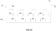
- FIGs. 22-24 are schematic views of a fifth embodiment of the electrode member of the present invention.
- the stripe-shape groove G of the fifth embodiment comprises a third groove G3 and a fourth groove G4, the third groove G3 and the fourth groove G4 are formed in the main portion 121.
- the third groove G3 is provided as multiple in number and the third grooves G3 are arranged to space apart from each other in the width direction X;
- the fourth groove G4 is provided as multiple in number and the fourth grooves G4 are arranged to space apart from each other in the width direction X.
- each third groove G3 is positioned between two adjacent fourth grooves G4.
- the third grooves G3 are alternated with the fourth grooves G4.
- the third grooves G3 and the fourth grooves G4 are arranged discretely in the width direction X and in the height direction Z, which can improve the releasing effect and uniformity of the stress.
Landscapes
- Chemical & Material Sciences (AREA)
- Chemical Kinetics & Catalysis (AREA)
- Electrochemistry (AREA)
- General Chemical & Material Sciences (AREA)
- Engineering & Computer Science (AREA)
- Manufacturing & Machinery (AREA)
- Composite Materials (AREA)
- Materials Engineering (AREA)
- Battery Electrode And Active Subsutance (AREA)
- Secondary Cells (AREA)
- Connection Of Batteries Or Terminals (AREA)
Abstract
Description
- The present application claims priority to Chinese patent application No.
CN201811183466.4, filed on October 11, 2018 - The present invention relates to the field of battery, and particularly relates to a secondary battery and an electrode member thereof.
- An electrode member of a secondary battery generally comprises a current collector and an active material layer coated on a surface of the current collector. In order to improve the safety performance of the secondary battery, some
electrode plates 1 choose a current collector in multi-layer structure; referring toFIG. 1 to FIG. 3 , the current collector comprises aninsulating substrate 11 and a conductinglayer 12 connected with a surface of theinsulating substrate 11, theactive material layer 13 is coated on a surface of the conductinglayer 12. - In the production process of the electrode member, the
active material layer 13 needs to be rolled and in turn become thin, thereby improving energy density. Theinsulating substrate 11 is made from a softer material such as PET (polyethylene terephthalate), the conductinglayer 12 is generally made of a metal, an elastic modulus of theinsulating substrate 11 is less than an elastic modulus of the conductinglayer 1, so an extensibility of theinsulating substrate 11 is greater than an extensibility of the conductinglayer 12. In the extending process of theinsulating substrate 11, theinsulating substrate 11 will apply a force to the conductinglayer 12; a connecting force between theinsulating substrate 11 and the conductinglayer 12 is small, so when theconducting layer 12 extends to a certain extent, the conductinglayer 12 may fall off from the surface of theinsulating substrate 11, thereby affecting performance of the electrode member. - In view of the problem existing in the background, an object of the present invention is to provide secondary battery and an electrode member thereof, which can reduce stress concentration, decrease the risk that the conducting layer falls off, and ensure performance of the electrode member.
- In order to achieve the above object, the present invention provides a secondary battery and an electrode member thereof.
- The electrode member comprises an insulating substrate, a first conducting layer and an active material layer; the first conducting layer is provided on a surface of the insulating substrate, the active material layer is provided at a side of the first conducting layer away from the insulating substrate; the first conducting layer is provided with a stripe-shape groove extending in a height direction of the electrode member.
- The electrode member further comprises a second conducting layer, the second conducting layer has a first portion provided in the stripe-shape groove.
- The second conducting layer further comprises a second portion, the second portion is provided on a surface of the first conducting layer away from the insulating substrate and connected with the first portion, the active material layer is provided on a surface of the second portion away from the first conducting layer.
- The first conducting layer comprises a main portion and a protruding portion extending from the main portion, the main portion is coated with the active material layer, the protruding portion is not coated with the active material layer. The stripe-shape groove comprises a first groove provided in the protruding portion, and at least a part of the second portion is provided on a surface of the protruding portion away from the insulating substrate.
- The stripe-shape groove further comprises a second groove provided in the main portion, the first groove is communicated with the second groove.
- The electrode member further comprises a protecting layer, the protecting layer is provided on a region of the second portion corresponding to the protruding portion and connected with the active material layer.
- A stiffness of the second conducting layer is less than a stiffness of the first conducting layer.
- The stripe-shape groove passes through the first conducting layer in a thickness direction of the electrode member, and the first portion of the second conducting layer is connected with the insulating substrate.
- The stripe-shape groove is provided as multiple in number, and the stripe-shape grooves are arranged to space apart from each other in a width direction of the electrode member.
- The secondary battery comprises an electrode assembly, the electrode assembly comprises the electrode member.
- The present invention has the following beneficial effects: in the present invention, the first conducting layer is provided with the stripe-shape groove, and the stripe-shape groove can effectively release the stress in the first conducting layer, reduce stress concentration, effectively decrease the risk that the first conducting layer falls off from the surface of the insulating substrate, and ensure performance of the electrode member.
-
-
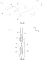
FIG. 1 is a schematic view of an electrode member in the prior art. -
FIG. 2 is a schematic view of the electrode member ofFIG. 1 in the process of rolling. -
FIG. 3 is a schematic view of an insulating substrate and a conducting layer of the electrode member ofFIG. 1 before rolling. -
FIG. 4 is a schematic view of the insulating substrate and the conducting layer of the electrode member ofFIG. 1 after rolling. -
FIG. 5 is a schematic view of a secondary battery according to the present invention. -
FIG. 6 is a cross sectional view of an electrode assembly according to the present invention. -
FIG. 7 is a schematic view of a first embodiment of the electrode member according to the present invention. -
FIG. 8 is a cross sectional view taken along a line A-A ofFIG. 7 . -
FIG. 9 is a schematic view of the electrode member ofFIG. 7 in the forming process. -
FIG. 10 is another schematic view of the electrode member ofFIG. 7 in the forming process. -
FIG. 11 is a schematic view of a first conducting layer ofFIG. 10 after rolling. -
FIG. 12 is still another schematic view of the electrode member ofFIG. 7 in the forming process. -
FIG. 13 is a schematic view of the electrode member ofFIG. 7 after winding. -
FIG. 14 is a schematic view of a second embodiment of the electrode member according to the present invention. -
FIG. 15 is a cross sectional view taken along a line B-B ofFIG. 14 . -
FIG. 16 is a schematic view of an insulating substrate and a first conducting layer ofFIG. 15 . -
FIG. 17 is a schematic view of a third embodiment of the electrode member according to the present invention. -
FIG. 18 is a cross sectional view taken along a line C-C ofFIG. 17 . -
FIG. 19 is a schematic view of a fourth embodiment of the electrode member according to the present invention. -
FIG. 20 is a cross sectional view taken along a line D-D ofFIG. 19 . -
FIG. 21 is a schematic view of the first conducting layer of the electrode member ofFIG. 19 . -
FIG. 22 is a schematic view of a fifth embodiment of the electrode member according to the present invention. -
FIG. 23 is a cross sectional view taken along a line E-E ofFIG. 22 . -
FIG. 24 is a schematic view of the first conducting layer of the electrode member ofFIG. 22 . - Reference numerals in figures are represented as follows:
- 1 electrode member
- 11 insulating substrate
- 12 first conducting layer
- 121 main portion
- 122 protruding portion
- 13 active material layer
- 14 second conducting layer
- 141 first portion
- 142 second portion
- 15 protecting layer
- 16 conductive structure
- 2 positive electrode member
- 3 negative electrode member
- 4 separator
- 5 case
- 6 cap plate
- 7 electrode terminal
- 8 connecting piece
- 9 roller
- G stripe-shape groove
- G1 first groove
- G2 second groove
- G3 third groove
- G4 fourth groove
- P electric guiding portion
- X width direction
- Y thickness direction
- Z height direction
- Hereinafter technical solutions of the embodiments of the present invention will be clearly and completely described in combination with the accompanying drawings in the embodiments of the present invention. Apparently, the described embodiments are a part rather than all of the embodiments of the present invention. The following description of at least one of the embodiments just is illustrative, and does not limit the present invention and the application or use thereof. All other embodiments obtained by the person skilled in the art based on the embodiments of the present invention without creative efforts shall fall within the protection scope of the present invention.
- In the description of the invention, it is necessary to understand that the words such as "first", "second" and the like are only used for defining the components, and distinguishing the components correspondingly, if there is no description, the words do not have any special meaning, so that it cannot be understood as limiting the protection scope of the present invention.
- A secondary battery of the present invention comprises an electrode assembly, referring to
FIG. 6 , the electrode assembly comprises apositive electrode member 2, anegative electrode member 3 and aseparator 4, theseparator 4 is provided between thepositive electrode member 2 and thenegative electrode member 3. Thepositive electrode member 2, theseparator 4 and thenegative electrode member 3 are stacked and wound to be a flat shape. The electrode assembly is a core component of the secondary battery to achieve a function of charge and discharge. - The secondary battery of the present invention can be a pouch-type battery; the electrode assembly formed by winding the
positive electrode member 2, theseparator 4 and thenegative electrode member 3 is directly packaged in a pouch. The pouch can be made of an aluminum plastic film. - Certainly, the secondary battery of the present invention also can be a can-type battery. Specifically, referring to
FIG. 5 , the secondary battery mainly comprises the electrode assembly, acase 5, acap plate 6, anelectrode terminal 7 and a connectingpiece 8. - The
case 5 can have a hexahedron shape or other shape. A receiving cavity is formed inside thecase 5 and receives the electrode assembly and an electrolyte. An opening is formed at an end of thecase 5, and the electrode assembly can be placed into the receiving cavity of thecase 5 via the opening. Thecase 5 can be made of a conductive metal such as aluminium, aluminium alloy and the like, and also can be made of an insulating material such as plastic. - The
cap plate 6 is provided to thecase 5 and covers the opening of thecase 5, thereby sealing the electrode assembly in thecase 5. Theelectrode terminal 7 is provided to thecap plate 6, an upper end of theelectrode terminal 7 protrudes above thecap plate 6, and a lower end of theelectrode terminal 7 can pass through thecap plate 6 and extend into thecase 5. The connectingpiece 8 is provided in thecase 5 and fixed with theelectrode terminal 7. Theelectrode terminal 7 and the connectingpiece 8 each are provided as two in number, thepositive electrode member 2 is electrically connected with oneelectrode terminal 7 via one connectingpiece 8, and thenegative electrode member 3 is electrically connected with theother electrode terminal 7 via the other connectingpiece 8. - In the secondary battery, at least one of the
positive electrode member 2 and thenegative electrode member 3 employs a later mentionedelectrode member 1. -
FIGs. 7-13 are schematic views of a first embodiment of anelectrode member 1 of the present invention. Referring toFIG. 7 andFIG. 8 , theelectrode member 1 of the first embodiment comprises an insulatingsubstrate 11, afirst conducting layer 12 and anactive material layer 13. Thefirst conducting layer 12 is provided on each of two surfaces of the insulatingsubstrate 11, theactive material layer 13 is provided at a side of thefirst conducting layer 12 away from the insulatingsubstrate 11. - The insulating
substrate 11 can be made of PET (polyethylene terephthalate) film or PP (polypropylene) film. - A material of the
first conducting layer 12 is one or more selected from a group consisting of metal conductive material and carbon-based conductive material; the metal conductive material is preferably one or more selected from a group consisting of aluminum, copper, nickel, titanium, silver, nickel copper alloy and aluminum zirconium alloy, the carbon-based conductive material is preferably one or more selected from a group consisting of graphite, acetylene carbon black, graphene and carbon nanotube. - The
first conducting layer 12 can be provided on the surface of the insulatingsubstrate 11 by at least one of the vapor deposition and the electroless plating. The vapor deposition is preferably a physical vapor deposition such as thermal evaporation deposition. - The
active material layer 13 can be provided on a surface of thefirst conducting layer 12 by coating. It can use an active material (such as lithium manganese oxide and lithium iron phosphate), a binder, a conductive agent and a solvent to prepare a slurry, then the slurry is coated on the outer surfaces of the two first conducting layers 12, and the slurry is dried to form theactive material layer 13. - Referring to
FIG. 9 , thefirst conducting layer 12 is provided with a stripe-shape groove G, the stripe-shape groove G extends generally in a height direction Z and is used for releasing stress of thefirst conducting layer 12. A length of the stripe-shape groove G in a width direction X is 0.001mm-1mm, and is much less than a length of the stripe-shape groove G extending in the height direction Z. The stripe-shape groove G can be in the shape of straight line or curve line, as long as the stripe-shape groove G overall approximately extends in the height direction Z; in other words, a smaller angle can exist between an extending direction of the stripe-shape groove G and the height direction Z, for example, the angle can be less than 10 degrees. - A thickness of the insulating
substrate 11 can be 1µm-20µm, a thickness of thefirst conducting layer 12 can be 0.1µm-10µm. Because thefirst conducting layer 12 is thin, in the process of cutting theelectrode member 1, a burr generated in thefirst conducting layer 12 is small, and difficult to pierce theseparator 4 more than ten micrometers, thereby avoiding short circuit and improving safety performance. In addition, when foreign matter pierces theelectrode member 1 of the secondary battery, the thickness of thefirst conducting layer 12 is small, so the burr generated in a part of thefirst conducting layer 12 pierced by the foreign matter is small, and difficult to pierce theseparator 4, thereby avoiding short circuit and improving safety performance. - The
first conducting layer 12 comprises amain portion 121 and a protrudingportion 122 extending from themain portion 121, themain portion 121 is coated with theactive material layer 13; the protrudingportion 122 is not coated with theactive material layer 13. Theactive material layer 13 can be directly coated on a surface of themain portion 121, alternatively, other material also can be provided between themain portion 121 and theactive material layer 13. - A part of the insulating
substrate 11 corresponding to the protrudingportion 122 and the protrudingportion 122 form an electric guiding portion P. The electric guiding portion P can be provided as multiple in number and the electric guiding portions P are arranged to space apart from each other in the width direction X. Referring toFIG. 13 , after winding, the electric guiding portions P of theelectrode member 1 stack in a thickness direction Y. - The
electrode member 1 further comprises a protectinglayer 15, the protectinglayer 15 is provided at a side of the protrudingportion 122 away from the insulatingsubstrate 11 and connected with theactive material layer 13. - The protecting
layer 15 comprises a binder and an insulating material. The insulating material comprises at least one of aluminum oxide and aluminum oxyhydroxide. The binder, the insulating material and a solvent are mixed to prepare a slurry, the slurry is coated on a surface of the protrudingportion 122 and dried to form the protectinglayer 15. A hardness of the protectinglayer 15 is greater than a hardness of the protrudingportion 122. - The
electrode member 1 further comprises aconductive structure 16, theconductive structure 16 is welded with a region of the protrudingportion 122 not covered by the protectinglayer 15. Referring toFIG. 7 andFIG. 8 , two sides of each electric guiding portion P in the thickness direction Y are fixed with theconductive structures 16. Referring toFIG. 13 , after winding, allconductive structures 16 of theelectrode member 1 stack and are welded with the connectingpiece 8 together. Referring toFIG. 5 , the electric current in theelectrode member 1 can be transmitted to the outside via the connectingpiece 8 and theelectrode terminal 7. - The
electrode member 1 of the first embodiment can be formed according to the following steps. - Step (i): forming a
first conducting layer 12 on a surface of the insulatingsubstrate 11 by vapor deposition or electroless plating, thereby preparing a composite strip; referring toFIG. 9 , in the forming process, a stripe-shape groove G is reserved for thefirst conducting layer 12. - Step (ii): referring to
FIG. 10 , coating anactive material layer 13 and a protectinglayer 15 on a surface of thefirst conducting layer 12 at the same time. - Step (iii): rolling the
active material layer 13 to thin theactive material layer 13 and improve density. - Step (iv): referring to
FIG. 12 , after rolling, welding a metal foil (such as aluminum foil) to thefirst conducting layer 12, then cutting along dotted lines inFIG. 12 to form a plurality of electric guiding portions P and a plurality ofconductive structures 16, thereby obtaining theelectrode member 1 shown inFIG. 7 . - In step (i), the
first conducting layer 12 is formed on the surface of the insulatingsubstrate 11 by vapor deposition or electroless plating, so the connecting force between thefirst conducting layer 12 and the insulatingsubstrate 11 is small; under the effect of external force, thefirst conducting layer 12 may be prone to fall off from the surface of the insulatingsubstrate 11. - Because an elastic modulus of the insulating
substrate 11 is less than an elastic modulus of thefirst conducting layer 12, an extensibility of the insulatingsubstrate 11 is greater than an extensibility of thefirst conducting layer 12. In step (iii), the insulatingsubstrate 11 extends due to rolling; the extensibility of the insulatingsubstrate 11 is greater, so the insulatingsubstrate 11 will apply a force to thefirst conducting layer 12. In the prior art, the stress in thefirst conducting layer 12 can not be released, so when thefirst conducting layer 12 extends to a certain extent, the stress in thefirst conducting layer 12 will be larger than the connecting force between the insulatingsubstrate 11 and thefirst conducting layer 12, thereby resulting in the insulatingsubstrate 11 and thefirst conducting layer 12 sliding relative to each other, and in turn leading to thefirst conducting layer 12 falling off from the surface of the insulatingsubstrate 11, affecting performance of theelectrode member 1. - In the present invention, the
first conducting layer 12 is provided with the stripe-shape groove G, and the stripe-shape groove G can effectively release the stress in thefirst conducting layer 12, reduce stress concentration, avoid the stress in thefirst conducting layer 12 being excessive, effectively decrease the risk that thefirst conducting layer 12 falls off from the surface of the insulatingsubstrate 11, and ensure performance of theelectrode member 1. - Specifically,
FIG. 11 shows a state of thefirst conducting layer 12 after rolling, the dotted lines shows a state of the stripe-shape groove G before rolling. In the rolling process of step (iii), the stress in thefirst conducting layer 12 gradually concentrates to the stripe-shape groove G; when the stress in thefirst conducting layer 12 is excessive, thefirst conducting layer 12 will be split along the stripe-shape groove G under the effect of the stress, thereby releasing the stress in time, avoiding the stress in thefirst conducting layer 12 being larger than the connecting force between the insulatingsubstrate 11 and thefirst conducting layer 12, decreasing probability that the insulatingsubstrate 11 and thefirst conducting layer 12 slide relative to each other, ensuring performance of theelectrode member 1. - In the working process of the secondary battery, the electric current generated in the
active material layer 13 flows to the protrudingportion 122 via themain portion 121, in other words, in thefirst conducting layer 12, the electric current generally flows in the height direction Z; therefore, the overcurrent area of thefirst conducting layer 12 depends on the area of a cross section of thefirst conducting layer 12 perpendicular to the height direction Z. In the present invention, the stripe-shape groove G generally extends in the height direction Z, the length of the stripe-shape groove G in the width direction X is very small; in other words, a dimension of the stripe-shape groove G in the height direction Z is larger than a dimension of the stripe-shape groove G in the width direction X. Therefore, when thefirst conducting layer 12 splits along the stripe-shape groove G in the rolling process, the effect of the stripe-shape groove G on the overcurrent area of thefirst conducting layer 12 is little, thereby ensuring that the overcurrent capability of thefirst conducting layer 12 meets the requirement. - In step (iii), with the rolling process going on, the stress in the
first conducting layer 12 will increase gradually; referring toFIG. 11 , when rolling theelectrode member 1 to a certain length in the width direction X, the stress in thefirst conducting layer 12 will bring thefirst conducting layer 12 to split along the stripe-shape groove G, thereby releasing the stress in time. Because thefirst conducting layer 12 has a larger length in the width direction X, the stripe-shape groove G is preferably provided as multiple in number, the stripe-shape grooves G in the width direction X are arranged to space apart from each other. The stripe-shape grooves G can release the stress gradually in the rolling process, thereby avoiding the stress in thefirst conducting layer 12 being larger than the connecting force between the insulatingsubstrate 11 and thefirst conducting layer 12, decreasing the probability that the insulatingsubstrate 11 and thefirst conducting layer 12 slide relative to each other, ensuring performance of theelectrode member 1. - Referring to
FIG. 8 and FIG. 9 , the stripe-shape groove G passes through thefirst conducting layer 12 in the thickness direction Y; in other words, a depth of the stripe-shape groove G is equal to the thickness of thefirst conducting layer 12 in the thickness direction Y. At this time, thefirst conducting layer 12 is more prone to split along the stripe-shape groove G in the rolling process, thereby releasing the stress in time. - In step (ii), the
active material layer 13 can be filled in the stripe-shape groove G, so the electric current in theactive material layer 13 can flow to thefirst conducting layer 12 via the peripheral wall of the stripe-shape groove G, thereby improving current collecting capability of thefirst conducting layer 12. In step (iii), even if thefirst conducting layer 12 split along the stripe-shape groove G, theactive material layer 13 still can be filled in the split portion under the effect of the rolling force. - Because the elastic modulus of the insulating
substrate 11 is small, in step (iii), the insulatingsubstrate 11 corresponding to themain portion 121 will extend to a lower side of the protrudingportion 122, which leads to the insulatingsubstrate 11 inside the protrudingportion 122 bulging, and the protrudingportion 122 is prone to deform under the effect of the insulatingsubstrate 11, thereby generating a crack. In the present invention, the protectinglayer 15 has a greater strength, so it can provide supporting force for the protrudingportion 122 in the process of rolling theelectrode member 1, thereby limiting the deformation of the protrudingportion 122, decreasing the probability of generating the crack in the protrudingportion 122, improving overcurrent capability of theelectrode member 1. - In the working process of the secondary battery, vibration and other factors may lead to the protruding
portion 122 falling off; the protectinglayer 15 is preferably connected with theactive material layer 13, so the protectinglayer 15 can be fixed with theactive material layer 13, thereby increasing the connecting force of the protectinglayer 15 in theelectrode member 1, improving anti-vibration capability, avoiding the protectinglayer 15 and the protrudingportion 122 falling off together. At the same time, the protrudingportion 122 is prone to bulge at the root portion (that is, a boundary between the protrudingportion 122 and the main portion 121) of the protrudingportion 122 close to theactive material layer 13, so when the protectinglayer 15 is connected with theactive material layer 13, it can decrease the deformation of the protrudingportion 122, reduce the probability of generating cracks, thereby improving the overcurrent capability of theelectrode member 1. - Hereinafter other four embodiments of the present invention will be described. In order to make description concise, hereinafter the differences between the other four embodiments and the first embodiment are mainly described, the part which is not described can be understood with reference to the first embodiment.
-
FIGs. 14-16 are schematic views of a second embodiment of the electrode member of the present invention. Referring toFIG. 14 andFIG. 16 , in the thickness direction Y, the depth of the stripe-shape groove G is less than the thickness of thefirst conducting layer 12. Compared to the first embodiment, thefirst conducting layer 12 of the second embodiment has a larger overcurrent area. The stripe-shape groove G can have a U-shaped cross-section or a V-shaped cross-section. -
FIG. 17 andFIG. 18 are schematic views of a third embodiment of the electrode member of the present invention. Referring toFIG. 17 andFIG. 18 , compared to the first embodiment, theelectrode member 1 of the third embodiment further comprises asecond conducting layer 14, thesecond conducting layer 14 has afirst portion 141 provided in the stripe-shape groove G. Thefirst portion 141 is filled in the stripe-shape groove G, the electric current around the stripe-shape groove G can be transmitted via thefirst portion 141; in other words, thefirst portion 141 can repair the conductive network of thefirst conducting layer 12, increase the overcurrent area and ensure whole overcurrent capability of theelectrode member 1. - In the first embodiment, the
active material layer 13 is filled in the stripe-shape groove G, so the distribution of theactive material layer 13 is not uniform; in other words, the thickness of theactive material layer 13 positioned in the stripe-shape groove G is larger than the thickness of theactive material layer 13 in other position. In the working process of the secondary battery, theactive material layer 13 may precipitate lithium in the position corresponding to the stripe-shape groove G. In the third embodiment, thefirst portion 141 is filled in the stripe-shape groove G, thereby ensuring flatness of thefirst conducting layer 12, improving the uniformity of distribution of theactive material layer 13, and reducing risk of precipitating lithium. - The
second conducting layer 14 further comprises asecond portion 142, thesecond portion 142 is provided on a surface of thefirst conducting layer 12 away from the insulatingsubstrate 11 and connected with thefirst portion 141, theactive material layer 13 is provided on a surface of thesecond portion 142 away from thefirst conducting layer 12. - The
second conducting layer 14 can be made of a metallic material or a non-metallic material. In order to decrease the burr generated when foreign matter pierces theelectrode member 1, thesecond conducting layer 14 is preferably made from a non-metallic material which is not prone to generate the burr. Specifically, it can use a conductive carbon, a binder and a solvent to prepare a slurry, the slurry is coated on thefirst conducting layer 12, and the slurry is dried to form thesecond conducting layer 14. In the coating process, the slurry is filled in the stripe-shape groove G to form thefirst portion 141. - In step (ii), the slurry of the
second conducting layer 14 is coated on thefirst conducting layer 12 firstly, and then the slurry of theactive material layer 13 and the slurry of the protectinglayer 15 are coated on the surface of thesecond conducting layer 14. - In step (iii), even if the
first conducting layer 12 splits along the stripe-shape groove G, thesecond portion 142 can be filled in the split portion under the effect of rolling force, thereby repairing the conductive network of thefirst conducting layer 12, increasing overcurrent area and ensuring whole overcurrent capability of theelectrode member 1. - If the
second conducting layer 14 is only provided on the surface of thefirst conducting layer 12, the electric current in thesecond conducting layer 14 only can be transmitted to thefirst conducting layer 12 via the surface of thefirst conducting layer 12. In the present invention, thefirst portion 141 of thesecond conducting layer 14 is filled in the stripe-shape groove G of thefirst conducting layer 12, so the electric current not only can be transmitted to thefirst conducting layer 12 via the surface of thefirst conducting layer 12, but also can be transmitted via the peripheral wall of the stripe-shape groove G, thereby increasing a plurality of conduction paths, forming a multi-point conductive network, improving conductive performance of theelectrode member 1, decreasing polarization of theelectrode member 1 and polarization of the secondary battery, improving high rate charge-discharge performance of the secondary battery. - At least a part of the
second portion 142 is provided on a surface of the protrudingportion 122 away from the insulatingsubstrate 11. The protectinglayer 15 can be provided on the surface of thesecond portion 142 away from the protrudingportion 122. Theconductive structure 16 is welded with a region of the protrudingportion 122 not covered by thesecond portion 142. - In step (iii), the
main portion 121 extends under the bring of the insulatingsubstrate 11, and the protrudingportion 122 almost does not extend. Themain portion 121 and the insulatingsubstrate 11 apply a force to the protrudingportion 122 when extending, because the protrudingportion 122 is thin, the protrudingportion 122 will generate a tiny crack under the effect of the force. In the present invention, thesecond portion 142 is provided on the surface of the protrudingportion 122, so even if the protrudingportion 122 generates a crack in the process of rolling, the electric current at the crack can be transmitted to the outside via thesecond portion 142, thereby repairing the conductive network and ensuring whole overcurrent capability of theelectrode member 1. - A stiffness of the
second conducting layer 14 is less than a stiffness of thefirst conducting layer 12. In other words, when thesecond conducting layer 14 is subjected to a force, thesecond conducting layer 14 deforms more easily. When the protrudingportion 122 deforms, thesecond portion 142 will deform with the protrudingportion 122; even if the protrudingportion 122 fractures due to an excessive deformation, thesecond portion 142 will not be prone to be fractured, thereby ensuring transmission of the electric current. - The stripe-shape groove G passes through the
first conducting layer 12 in the thickness direction Y, and thefirst portion 141 of thesecond conducting layer 14 is connected with the insulatingsubstrate 11. Thefirst portion 141 is filled in the stripe-shape groove G and bonded to the insulatingsubstrate 11, thereby increasing the connecting strength among thefirst conducting layer 12, thesecond conducting layer 14 and the insulatingsubstrate 11. -
FIGs. 19-21 are schematic views of a fourth embodiment of the electrode member of the present invention. Referring toFIG. 19 to FIG. 21 , compared to the third embodiment, the stripe-shape groove G of the fourth embodiment comprises a first groove G1 formed in the protrudingportion 122. - In step (iii), a part of the insulating
substrate 11 corresponding to themain portion 121 extends under the effect of rolling, the part of the insulatingsubstrate 11 corresponding to themain portion 121 will apply a force to a part of the insulatingsubstrate 11 corresponding to the protrudingportion 122, thereby bringing the part of the insulatingsubstrate 11 corresponding to the protrudingportion 122 to extend. Because the protrudingportion 122 is limited by the protectinglayer 15, the protrudingportion 122 almost does not extend; the part of the insulatingsubstrate 11 corresponding to protrudingportion 122 will apply an acting force to the protrudingportion 122 when extending, if the acting force is larger than the connecting force between the insulatingsubstrate 11 and the protrudingportion 122, the protrudingportion 122 will be prone to fall off from the insulatingsubstrate 11. In the present invention, the first groove G1 can effectively release the acting force applied to the protrudingportion 122, reduce stress concentration, avoid the acting force applied to the protrudingportion 122 being excessive, effectively decrease the probability that the protrudingportion 122 falls off, and ensure performance of theelectrode member 1. - Preferably, in a direction away from the
active material layer 13, the first groove G1 is not beyond the protectinglayer 15. The acting force subjected by the protrudingportion 122 is maximum at a region of the protrudingportion 122 covered by the protectinglayer 15, so the first groove G1 only needs to be provided in the region of the protrudingportion 122 covered by the protectinglayer 15. The acting force subjected by the protrudingportion 122 is smaller at a region of the protrudingportion 122 not covered by the protectinglayer 15, so there is no risk of falling off; if the first groove G1 extends to the region of the protrudingportion 122 not covered by the protectinglayer 15, the overcurrent capability of the protrudingportion 122 will be reduced instead. - The stripe-shape groove G further comprises a second groove G2 formed in the
main portion 121, the first groove G1 is communicated with the second groove G2. - In step (iii), the
main portion 121 extends under the force applied by the insulatingsubstrate 11. Because the protrudingportion 122 is limited by the protectinglayer 15, the protrudingportion 122 almost does not extend, a region of themain portion 121 close to the protrudingportion 122 is subjected to a reaction force of the protrudingportion 122. In other words, the region of themain portion 121 close to the protrudingportion 122 is subjected to the force of the insulatingsubstrate 11 and the reaction force of the protrudingportion 122 at the same time, so the region of themain portion 121 close to the protrudingportion 122 is more prone to fall off from the insulatingsubstrate 11. However, in the present invention, the second groove G2 extends to the region of themain portion 121 close to the protrudingportion 122, thereby effectively releasing the forces in themain portion 121, reduce stress concentration, effectively decrease the probability that the insulatingsubstrate 11 and themain portion 121 slide relative to each other, ensure performance of theelectrode member 1. - The stripe-shape groove G further comprises a plurality of third grooves G3, the third grooves G3 are arranged to space apart from each other in the width direction X, and the third grooves G3 are formed in
main portion 121. In the width direction X, each third groove G3 is positioned between two adjacent second grooves G2; in the height direction Z, the third grooves G3 are alternated with the second grooves G2. -
FIGs. 22-24 are schematic views of a fifth embodiment of the electrode member of the present invention. Referring toFIG. 22 to FIG. 24 , the stripe-shape groove G of the fifth embodiment comprises a third groove G3 and a fourth groove G4, the third groove G3 and the fourth groove G4 are formed in themain portion 121. The third groove G3 is provided as multiple in number and the third grooves G3 are arranged to space apart from each other in the width direction X; the fourth groove G4 is provided as multiple in number and the fourth grooves G4 are arranged to space apart from each other in the width direction X. - In the width direction X, each third groove G3 is positioned between two adjacent fourth grooves G4. In the height direction Z, the third grooves G3 are alternated with the fourth grooves G4. The third grooves G3 and the fourth grooves G4 are arranged discretely in the width direction X and in the height direction Z, which can improve the releasing effect and uniformity of the stress.
Claims (10)
- An electrode member (1) of a secondary battery, comprising an insulating substrate (11), a first conducting layer (12) and an active material layer (13);
the first conducting layer (12) being provided on a surface of the insulating substrate (11), the active material layer (13) being provided at a side of the first conducting layer (12) away from the insulating substrate (11);
the first conducting layer (12) being provided with a stripe-shape groove (G) extending in a height direction (Z) of the electrode member (1). - The electrode member (1) according to Claim 1, wherein
the electrode member (1) further comprises a second conducting layer (14), the second conducting layer (14) has a first portion (141) provided in the stripe-shape groove (G). - The electrode member (1) according to Claim 2, wherein
the second conducting layer (14) further comprises a second portion (142), the second portion (142) is provided on a surface of the first conducting layer (12) away from the insulating substrate (11) and connected with the first portion (141), the active material layer (13) is provided on a surface of the second portion (142) away from the first conducting layer (12). - The electrode member (1) according to Claim 3, wherein
the first conducting layer (12) comprises a main portion (121) and a protruding portion (122) extending from the main portion (121), the main portion (121) is coated with the active material layer (13), the protruding portion (122) is not coated with the active material layer (13);
the stripe-shape groove (G) comprises a first groove (G1) provided in the protruding portion (122), and at least a part of the second portion (142) is provided on a surface of the protruding portion (122) away from the insulating substrate (11). - The electrode member (1) according to Claim 4, wherein
the stripe-shape groove (G) further comprises a second groove (G2) provided in the main portion (121), the first groove (G1) is communicated with the second groove (G2). - The electrode member (1) according to Claim 4 or 5, wherein
the electrode member (1) further comprises a protecting layer (15), the protecting layer (15) is provided on a region of the second portion (142) corresponding to the protruding portion (122) and connected with the active material layer (13). - The electrode member (1) according to any one of Claims 2 to 6, wherein
a stiffness of the second conducting layer (14) is less than a stiffness of the first conducting layer (12). - The electrode member (1) according to any one of Claims 2 to 7, wherein
the stripe-shape groove (G) passes through the first conducting layer (12) in a thickness direction (Y) of the electrode member (1), and the first portion (141) of the second conducting layer (14) is connected with the insulating substrate (11). - The electrode member (1) according to any one of Claims 1 to 8, wherein
the stripe-shape groove (G) is provided as multiple in number, and the stripe-shape grooves (G) are arranged to space apart from each other in a width direction (X) of the electrode member (1). - A secondary battery, comprising an electrode assembly; the electrode assembly comprising the electrode member (1) according to any one of Claims 1 to 9.
Priority Applications (1)
| Application Number | Priority Date | Filing Date | Title |
|---|---|---|---|
| PL19153878T PL3637515T3 (en) | 2018-10-11 | 2019-01-28 | Secondary battery and electrode member thereof |
Applications Claiming Priority (1)
| Application Number | Priority Date | Filing Date | Title |
|---|---|---|---|
| CN201811183466.4A CN111048791A (en) | 2018-10-11 | 2018-10-11 | Secondary battery and electrode member thereof |
Publications (2)
| Publication Number | Publication Date |
|---|---|
| EP3637515A1 true EP3637515A1 (en) | 2020-04-15 |
| EP3637515B1 EP3637515B1 (en) | 2021-01-13 |
Family
ID=65236944
Family Applications (1)
| Application Number | Title | Priority Date | Filing Date |
|---|---|---|---|
| EP19153878.4A Active EP3637515B1 (en) | 2018-10-11 | 2019-01-28 | Secondary battery and electrode member thereof |
Country Status (4)
| Country | Link |
|---|---|
| US (1) | US11101493B2 (en) |
| EP (1) | EP3637515B1 (en) |
| CN (2) | CN111048791A (en) |
| PL (1) | PL3637515T3 (en) |
Families Citing this family (3)
| Publication number | Priority date | Publication date | Assignee | Title |
|---|---|---|---|---|
| CN111048791A (en) * | 2018-10-11 | 2020-04-21 | 宁德时代新能源科技股份有限公司 | Secondary battery and electrode member thereof |
| TWI779502B (en) * | 2021-02-25 | 2022-10-01 | 宏碁股份有限公司 | Electronic device and method for suppressing battery swelling |
| CN115863536A (en) * | 2021-09-27 | 2023-03-28 | 宁德时代新能源科技股份有限公司 | Electrode assembly, manufacturing method and system thereof, battery cell, battery and electric device |
Citations (2)
| Publication number | Priority date | Publication date | Assignee | Title |
|---|---|---|---|---|
| US20130011742A1 (en) * | 2010-03-26 | 2013-01-10 | Unist Academy-Industry Research Corporation | Current collector for flexible electrode, method of manufacturing same, and negative electrode including same |
| CN108155387A (en) * | 2016-12-06 | 2018-06-12 | 华为技术有限公司 | A kind of elastic collector and preparation method thereof, cell electrode piece and flexible lithium ion battery |
Family Cites Families (17)
| Publication number | Priority date | Publication date | Assignee | Title |
|---|---|---|---|---|
| JP2011076836A (en) * | 2009-09-30 | 2011-04-14 | Panasonic Corp | Electrode for secondary battery and the secondary battery |
| SE537449C2 (en) * | 2012-04-04 | 2015-05-05 | Exeger Sweden Ab | A dye-sensitized solar cell containing a porous insulating substrate and a method of producing the porous insulating substrate |
| JP2015011775A (en) | 2013-06-26 | 2015-01-19 | 株式会社東芝 | Lithium ion secondary battery |
| US10008739B2 (en) * | 2015-02-23 | 2018-06-26 | Front Edge Technology, Inc. | Solid-state lithium battery with electrolyte |
| JP6619594B2 (en) * | 2015-09-17 | 2019-12-11 | 積水化学工業株式会社 | Lithium ion secondary battery and manufacturing method thereof |
| JP6859059B2 (en) * | 2015-09-30 | 2021-04-14 | 積水化学工業株式会社 | Lithium-ion secondary battery and its manufacturing method |
| CN205303580U (en) | 2016-01-22 | 2016-06-08 | 宁德时代新能源科技股份有限公司 | Lithium ion battery pole piece and contain lithium ion battery of this pole piece |
| CN108428848B (en) * | 2017-11-22 | 2021-03-26 | 宁德时代新能源科技股份有限公司 | Electrode member, electrode assembly and rechargeable battery |
| CN207542313U (en) | 2017-11-22 | 2018-06-26 | 宁德时代新能源科技股份有限公司 | Electrode member, electrode assembly and rechargeable battery |
| CN108417841B (en) | 2018-02-09 | 2021-08-03 | 深圳前海优容科技有限公司 | Battery, battery cell, current collector and preparation method thereof |
| CN207818780U (en) | 2018-02-13 | 2018-09-04 | 宁德时代新能源科技股份有限公司 | Collector, pole piece and battery |
| CN111883740B (en) * | 2018-06-22 | 2021-09-21 | 宁德时代新能源科技股份有限公司 | Pole piece and secondary battery |
| CN208955090U (en) * | 2018-09-27 | 2019-06-07 | 宁德时代新能源科技股份有限公司 | Secondary cell and its electrode member |
| CN208955108U (en) * | 2018-10-11 | 2019-06-07 | 宁德时代新能源科技股份有限公司 | Secondary cell and its electrode member |
| CN111048791A (en) * | 2018-10-11 | 2020-04-21 | 宁德时代新能源科技股份有限公司 | Secondary battery and electrode member thereof |
| CN110660956A (en) * | 2018-10-17 | 2020-01-07 | 宁德时代新能源科技股份有限公司 | Secondary battery and electrode member thereof |
| CN209401736U (en) * | 2019-01-28 | 2019-09-17 | 宁德时代新能源科技股份有限公司 | Electrode member, electrode assembly and secondary cell |
-
2018
- 2018-10-11 CN CN201811183466.4A patent/CN111048791A/en active Pending
- 2018-10-11 CN CN202110446847.2A patent/CN113224316B/en active Active
-
2019
- 2019-01-28 PL PL19153878T patent/PL3637515T3/en unknown
- 2019-01-28 EP EP19153878.4A patent/EP3637515B1/en active Active
- 2019-02-05 US US16/268,364 patent/US11101493B2/en active Active
Patent Citations (2)
| Publication number | Priority date | Publication date | Assignee | Title |
|---|---|---|---|---|
| US20130011742A1 (en) * | 2010-03-26 | 2013-01-10 | Unist Academy-Industry Research Corporation | Current collector for flexible electrode, method of manufacturing same, and negative electrode including same |
| CN108155387A (en) * | 2016-12-06 | 2018-06-12 | 华为技术有限公司 | A kind of elastic collector and preparation method thereof, cell electrode piece and flexible lithium ion battery |
Also Published As
| Publication number | Publication date |
|---|---|
| EP3637515B1 (en) | 2021-01-13 |
| CN111048791A (en) | 2020-04-21 |
| CN113224316B (en) | 2022-07-08 |
| US20200119389A1 (en) | 2020-04-16 |
| PL3637515T3 (en) | 2021-06-28 |
| US11101493B2 (en) | 2021-08-24 |
| CN113224316A (en) | 2021-08-06 |
Similar Documents
| Publication | Publication Date | Title |
|---|---|---|
| EP3985763B1 (en) | Electrode assembly and battery unit | |
| US10103376B2 (en) | Stacked all-solid-state battery | |
| WO2020073887A1 (en) | Secondary battery and manufacturing method therefor, electrode component and manufacturing method therefor, and manufacturing method for current collector | |
| US11444284B2 (en) | Secondary battery and electrode member thereof capable of being decreased bending deformation after rolling | |
| EP3637515B1 (en) | Secondary battery and electrode member thereof | |
| JP6575557B2 (en) | All-solid battery and method for producing all-solid battery | |
| EP3637504B1 (en) | Secondary battery and electrode plate thereof | |
| US11855304B2 (en) | Secondary battery | |
| KR20130087968A (en) | Electrode assembly and secondary battery comprising the same | |
| EP4311014A1 (en) | Cylindrical secondary battery | |
| WO2023013233A1 (en) | Battery | |
| US20220384802A1 (en) | Solid-state battery and method of manufacturing solid-state battery | |
| CN114649535B (en) | Electrode for secondary battery | |
| US20230163426A1 (en) | Battery cell | |
| CN210403926U (en) | Secondary battery and electrode member thereof | |
| US20220384803A1 (en) | Solid-state battery and method of manufacturing solid-state battery | |
| EP4376209A1 (en) | Cell pack and power battery | |
| JP2023180579A (en) | battery | |
| JP2014170614A (en) | Electrode for electrochemical element and electrochemical element |
Legal Events
| Date | Code | Title | Description |
|---|---|---|---|
| PUAI | Public reference made under article 153(3) epc to a published international application that has entered the european phase |
Free format text: ORIGINAL CODE: 0009012 |
|
| STAA | Information on the status of an ep patent application or granted ep patent |
Free format text: STATUS: REQUEST FOR EXAMINATION WAS MADE |
|
| 17P | Request for examination filed |
Effective date: 20190128 |
|
| AK | Designated contracting states |
Kind code of ref document: A1 Designated state(s): AL AT BE BG CH CY CZ DE DK EE ES FI FR GB GR HR HU IE IS IT LI LT LU LV MC MK MT NL NO PL PT RO RS SE SI SK SM TR |
|
| AX | Request for extension of the european patent |
Extension state: BA ME |
|
| GRAP | Despatch of communication of intention to grant a patent |
Free format text: ORIGINAL CODE: EPIDOSNIGR1 |
|
| STAA | Information on the status of an ep patent application or granted ep patent |
Free format text: STATUS: GRANT OF PATENT IS INTENDED |
|
| INTG | Intention to grant announced |
Effective date: 20200826 |
|
| GRAS | Grant fee paid |
Free format text: ORIGINAL CODE: EPIDOSNIGR3 |
|
| GRAA | (expected) grant |
Free format text: ORIGINAL CODE: 0009210 |
|
| STAA | Information on the status of an ep patent application or granted ep patent |
Free format text: STATUS: THE PATENT HAS BEEN GRANTED |
|
| AK | Designated contracting states |
Kind code of ref document: B1 Designated state(s): AL AT BE BG CH CY CZ DE DK EE ES FI FR GB GR HR HU IE IS IT LI LT LU LV MC MK MT NL NO PL PT RO RS SE SI SK SM TR |
|
| REG | Reference to a national code |
Ref country code: GB Ref legal event code: FG4D |
|
| REG | Reference to a national code |
Ref country code: CH Ref legal event code: EP |
|
| REG | Reference to a national code |
Ref country code: DE Ref legal event code: R096 Ref document number: 602019002104 Country of ref document: DE |
|
| REG | Reference to a national code |
Ref country code: IE Ref legal event code: FG4D |
|
| REG | Reference to a national code |
Ref country code: AT Ref legal event code: REF Ref document number: 1355230 Country of ref document: AT Kind code of ref document: T Effective date: 20210215 |
|
| REG | Reference to a national code |
Ref country code: SE Ref legal event code: TRGR |
|
| REG | Reference to a national code |
Ref country code: NL Ref legal event code: FP |
|
| REG | Reference to a national code |
Ref country code: AT Ref legal event code: MK05 Ref document number: 1355230 Country of ref document: AT Kind code of ref document: T Effective date: 20210113 |
|
| REG | Reference to a national code |
Ref country code: LT Ref legal event code: MG9D |
|
| PG25 | Lapsed in a contracting state [announced via postgrant information from national office to epo] |
Ref country code: GR Free format text: LAPSE BECAUSE OF FAILURE TO SUBMIT A TRANSLATION OF THE DESCRIPTION OR TO PAY THE FEE WITHIN THE PRESCRIBED TIME-LIMIT Effective date: 20210414 Ref country code: FI Free format text: LAPSE BECAUSE OF FAILURE TO SUBMIT A TRANSLATION OF THE DESCRIPTION OR TO PAY THE FEE WITHIN THE PRESCRIBED TIME-LIMIT Effective date: 20210113 Ref country code: HR Free format text: LAPSE BECAUSE OF FAILURE TO SUBMIT A TRANSLATION OF THE DESCRIPTION OR TO PAY THE FEE WITHIN THE PRESCRIBED TIME-LIMIT Effective date: 20210113 Ref country code: BG Free format text: LAPSE BECAUSE OF FAILURE TO SUBMIT A TRANSLATION OF THE DESCRIPTION OR TO PAY THE FEE WITHIN THE PRESCRIBED TIME-LIMIT Effective date: 20210413 Ref country code: PT Free format text: LAPSE BECAUSE OF FAILURE TO SUBMIT A TRANSLATION OF THE DESCRIPTION OR TO PAY THE FEE WITHIN THE PRESCRIBED TIME-LIMIT Effective date: 20210513 Ref country code: NO Free format text: LAPSE BECAUSE OF FAILURE TO SUBMIT A TRANSLATION OF THE DESCRIPTION OR TO PAY THE FEE WITHIN THE PRESCRIBED TIME-LIMIT Effective date: 20210413 Ref country code: LT Free format text: LAPSE BECAUSE OF FAILURE TO SUBMIT A TRANSLATION OF THE DESCRIPTION OR TO PAY THE FEE WITHIN THE PRESCRIBED TIME-LIMIT Effective date: 20210113 |
|
| PG25 | Lapsed in a contracting state [announced via postgrant information from national office to epo] |
Ref country code: RS Free format text: LAPSE BECAUSE OF FAILURE TO SUBMIT A TRANSLATION OF THE DESCRIPTION OR TO PAY THE FEE WITHIN THE PRESCRIBED TIME-LIMIT Effective date: 20210113 Ref country code: LV Free format text: LAPSE BECAUSE OF FAILURE TO SUBMIT A TRANSLATION OF THE DESCRIPTION OR TO PAY THE FEE WITHIN THE PRESCRIBED TIME-LIMIT Effective date: 20210113 Ref country code: AT Free format text: LAPSE BECAUSE OF FAILURE TO SUBMIT A TRANSLATION OF THE DESCRIPTION OR TO PAY THE FEE WITHIN THE PRESCRIBED TIME-LIMIT Effective date: 20210113 |
|
| PG25 | Lapsed in a contracting state [announced via postgrant information from national office to epo] |
Ref country code: LU Free format text: LAPSE BECAUSE OF NON-PAYMENT OF DUE FEES Effective date: 20210128 Ref country code: IS Free format text: LAPSE BECAUSE OF FAILURE TO SUBMIT A TRANSLATION OF THE DESCRIPTION OR TO PAY THE FEE WITHIN THE PRESCRIBED TIME-LIMIT Effective date: 20210513 |
|
| REG | Reference to a national code |
Ref country code: DE Ref legal event code: R097 Ref document number: 602019002104 Country of ref document: DE |
|
| PG25 | Lapsed in a contracting state [announced via postgrant information from national office to epo] |
Ref country code: SM Free format text: LAPSE BECAUSE OF FAILURE TO SUBMIT A TRANSLATION OF THE DESCRIPTION OR TO PAY THE FEE WITHIN THE PRESCRIBED TIME-LIMIT Effective date: 20210113 Ref country code: CZ Free format text: LAPSE BECAUSE OF FAILURE TO SUBMIT A TRANSLATION OF THE DESCRIPTION OR TO PAY THE FEE WITHIN THE PRESCRIBED TIME-LIMIT Effective date: 20210113 Ref country code: EE Free format text: LAPSE BECAUSE OF FAILURE TO SUBMIT A TRANSLATION OF THE DESCRIPTION OR TO PAY THE FEE WITHIN THE PRESCRIBED TIME-LIMIT Effective date: 20210113 Ref country code: MC Free format text: LAPSE BECAUSE OF FAILURE TO SUBMIT A TRANSLATION OF THE DESCRIPTION OR TO PAY THE FEE WITHIN THE PRESCRIBED TIME-LIMIT Effective date: 20210113 |
|
| PLBE | No opposition filed within time limit |
Free format text: ORIGINAL CODE: 0009261 |
|
| STAA | Information on the status of an ep patent application or granted ep patent |
Free format text: STATUS: NO OPPOSITION FILED WITHIN TIME LIMIT |
|
| PG25 | Lapsed in a contracting state [announced via postgrant information from national office to epo] |
Ref country code: DK Free format text: LAPSE BECAUSE OF FAILURE TO SUBMIT A TRANSLATION OF THE DESCRIPTION OR TO PAY THE FEE WITHIN THE PRESCRIBED TIME-LIMIT Effective date: 20210113 Ref country code: SK Free format text: LAPSE BECAUSE OF FAILURE TO SUBMIT A TRANSLATION OF THE DESCRIPTION OR TO PAY THE FEE WITHIN THE PRESCRIBED TIME-LIMIT Effective date: 20210113 Ref country code: RO Free format text: LAPSE BECAUSE OF FAILURE TO SUBMIT A TRANSLATION OF THE DESCRIPTION OR TO PAY THE FEE WITHIN THE PRESCRIBED TIME-LIMIT Effective date: 20210113 |
|
| 26N | No opposition filed |
Effective date: 20211014 |
|
| PG25 | Lapsed in a contracting state [announced via postgrant information from national office to epo] |
Ref country code: ES Free format text: LAPSE BECAUSE OF FAILURE TO SUBMIT A TRANSLATION OF THE DESCRIPTION OR TO PAY THE FEE WITHIN THE PRESCRIBED TIME-LIMIT Effective date: 20210113 Ref country code: AL Free format text: LAPSE BECAUSE OF FAILURE TO SUBMIT A TRANSLATION OF THE DESCRIPTION OR TO PAY THE FEE WITHIN THE PRESCRIBED TIME-LIMIT Effective date: 20210113 Ref country code: IE Free format text: LAPSE BECAUSE OF NON-PAYMENT OF DUE FEES Effective date: 20210128 |
|
| PG25 | Lapsed in a contracting state [announced via postgrant information from national office to epo] |
Ref country code: SI Free format text: LAPSE BECAUSE OF FAILURE TO SUBMIT A TRANSLATION OF THE DESCRIPTION OR TO PAY THE FEE WITHIN THE PRESCRIBED TIME-LIMIT Effective date: 20210113 |
|
| PG25 | Lapsed in a contracting state [announced via postgrant information from national office to epo] |
Ref country code: IS Free format text: LAPSE BECAUSE OF FAILURE TO SUBMIT A TRANSLATION OF THE DESCRIPTION OR TO PAY THE FEE WITHIN THE PRESCRIBED TIME-LIMIT Effective date: 20210513 |
|
| REG | Reference to a national code |
Ref country code: CH Ref legal event code: PL |
|
| PG25 | Lapsed in a contracting state [announced via postgrant information from national office to epo] |
Ref country code: LI Free format text: LAPSE BECAUSE OF NON-PAYMENT OF DUE FEES Effective date: 20220131 Ref country code: CH Free format text: LAPSE BECAUSE OF NON-PAYMENT OF DUE FEES Effective date: 20220131 |
|
| PGFP | Annual fee paid to national office [announced via postgrant information from national office to epo] |
Ref country code: IT Payment date: 20221213 Year of fee payment: 5 |
|
| P01 | Opt-out of the competence of the unified patent court (upc) registered |
Effective date: 20230516 |
|
| PG25 | Lapsed in a contracting state [announced via postgrant information from national office to epo] |
Ref country code: CY Free format text: LAPSE BECAUSE OF FAILURE TO SUBMIT A TRANSLATION OF THE DESCRIPTION OR TO PAY THE FEE WITHIN THE PRESCRIBED TIME-LIMIT Effective date: 20210113 |
|
| PG25 | Lapsed in a contracting state [announced via postgrant information from national office to epo] |
Ref country code: HU Free format text: LAPSE BECAUSE OF FAILURE TO SUBMIT A TRANSLATION OF THE DESCRIPTION OR TO PAY THE FEE WITHIN THE PRESCRIBED TIME-LIMIT; INVALID AB INITIO Effective date: 20190128 |
|
| PGFP | Annual fee paid to national office [announced via postgrant information from national office to epo] |
Ref country code: GB Payment date: 20231207 Year of fee payment: 6 |
|
| PGFP | Annual fee paid to national office [announced via postgrant information from national office to epo] |
Ref country code: SE Payment date: 20231213 Year of fee payment: 6 Ref country code: NL Payment date: 20231215 Year of fee payment: 6 Ref country code: FR Payment date: 20231212 Year of fee payment: 6 |
|
| PGFP | Annual fee paid to national office [announced via postgrant information from national office to epo] |
Ref country code: PL Payment date: 20231129 Year of fee payment: 6 Ref country code: BE Payment date: 20231219 Year of fee payment: 6 |
|
| PG25 | Lapsed in a contracting state [announced via postgrant information from national office to epo] |
Ref country code: MK Free format text: LAPSE BECAUSE OF FAILURE TO SUBMIT A TRANSLATION OF THE DESCRIPTION OR TO PAY THE FEE WITHIN THE PRESCRIBED TIME-LIMIT Effective date: 20210113 |
|
| PGFP | Annual fee paid to national office [announced via postgrant information from national office to epo] |
Ref country code: DE Payment date: 20231205 Year of fee payment: 6 |