EP3637504A1 - Secondary battery and electrode plate thereof - Google Patents
Secondary battery and electrode plate thereof Download PDFInfo
- Publication number
- EP3637504A1 EP3637504A1 EP19153877.6A EP19153877A EP3637504A1 EP 3637504 A1 EP3637504 A1 EP 3637504A1 EP 19153877 A EP19153877 A EP 19153877A EP 3637504 A1 EP3637504 A1 EP 3637504A1
- Authority
- EP
- European Patent Office
- Prior art keywords
- layer
- electrode plate
- conducting layer
- active material
- protruding portion
- Prior art date
- Legal status (The legal status is an assumption and is not a legal conclusion. Google has not performed a legal analysis and makes no representation as to the accuracy of the status listed.)
- Granted
Links
Images

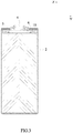


Classifications
-
- H—ELECTRICITY
- H01—ELECTRIC ELEMENTS
- H01M—PROCESSES OR MEANS, e.g. BATTERIES, FOR THE DIRECT CONVERSION OF CHEMICAL ENERGY INTO ELECTRICAL ENERGY
- H01M4/00—Electrodes
- H01M4/02—Electrodes composed of, or comprising, active material
- H01M4/64—Carriers or collectors
- H01M4/66—Selection of materials
- H01M4/665—Composites
- H01M4/667—Composites in the form of layers, e.g. coatings
-
- H—ELECTRICITY
- H01—ELECTRIC ELEMENTS
- H01M—PROCESSES OR MEANS, e.g. BATTERIES, FOR THE DIRECT CONVERSION OF CHEMICAL ENERGY INTO ELECTRICAL ENERGY
- H01M10/00—Secondary cells; Manufacture thereof
- H01M10/04—Construction or manufacture in general
- H01M10/0436—Small-sized flat cells or batteries for portable equipment
-
- H—ELECTRICITY
- H01—ELECTRIC ELEMENTS
- H01M—PROCESSES OR MEANS, e.g. BATTERIES, FOR THE DIRECT CONVERSION OF CHEMICAL ENERGY INTO ELECTRICAL ENERGY
- H01M4/00—Electrodes
- H01M4/02—Electrodes composed of, or comprising, active material
-
- H—ELECTRICITY
- H01—ELECTRIC ELEMENTS
- H01M—PROCESSES OR MEANS, e.g. BATTERIES, FOR THE DIRECT CONVERSION OF CHEMICAL ENERGY INTO ELECTRICAL ENERGY
- H01M10/00—Secondary cells; Manufacture thereof
- H01M10/05—Accumulators with non-aqueous electrolyte
- H01M10/052—Li-accumulators
-
- H—ELECTRICITY
- H01—ELECTRIC ELEMENTS
- H01M—PROCESSES OR MEANS, e.g. BATTERIES, FOR THE DIRECT CONVERSION OF CHEMICAL ENERGY INTO ELECTRICAL ENERGY
- H01M4/00—Electrodes
- H01M4/02—Electrodes composed of, or comprising, active material
- H01M2004/021—Physical characteristics, e.g. porosity, surface area
-
- H—ELECTRICITY
- H01—ELECTRIC ELEMENTS
- H01M—PROCESSES OR MEANS, e.g. BATTERIES, FOR THE DIRECT CONVERSION OF CHEMICAL ENERGY INTO ELECTRICAL ENERGY
- H01M50/00—Constructional details or processes of manufacture of the non-active parts of electrochemical cells other than fuel cells, e.g. hybrid cells
- H01M50/50—Current conducting connections for cells or batteries
- H01M50/531—Electrode connections inside a battery casing
- H01M50/534—Electrode connections inside a battery casing characterised by the material of the leads or tabs
-
- H—ELECTRICITY
- H01—ELECTRIC ELEMENTS
- H01M—PROCESSES OR MEANS, e.g. BATTERIES, FOR THE DIRECT CONVERSION OF CHEMICAL ENERGY INTO ELECTRICAL ENERGY
- H01M50/00—Constructional details or processes of manufacture of the non-active parts of electrochemical cells other than fuel cells, e.g. hybrid cells
- H01M50/50—Current conducting connections for cells or batteries
- H01M50/531—Electrode connections inside a battery casing
- H01M50/536—Electrode connections inside a battery casing characterised by the method of fixing the leads to the electrodes, e.g. by welding
-
- H—ELECTRICITY
- H01—ELECTRIC ELEMENTS
- H01M—PROCESSES OR MEANS, e.g. BATTERIES, FOR THE DIRECT CONVERSION OF CHEMICAL ENERGY INTO ELECTRICAL ENERGY
- H01M50/00—Constructional details or processes of manufacture of the non-active parts of electrochemical cells other than fuel cells, e.g. hybrid cells
- H01M50/50—Current conducting connections for cells or batteries
- H01M50/531—Electrode connections inside a battery casing
- H01M50/538—Connection of several leads or tabs of wound or folded electrode stacks
-
- Y—GENERAL TAGGING OF NEW TECHNOLOGICAL DEVELOPMENTS; GENERAL TAGGING OF CROSS-SECTIONAL TECHNOLOGIES SPANNING OVER SEVERAL SECTIONS OF THE IPC; TECHNICAL SUBJECTS COVERED BY FORMER USPC CROSS-REFERENCE ART COLLECTIONS [XRACs] AND DIGESTS
- Y02—TECHNOLOGIES OR APPLICATIONS FOR MITIGATION OR ADAPTATION AGAINST CLIMATE CHANGE
- Y02E—REDUCTION OF GREENHOUSE GAS [GHG] EMISSIONS, RELATED TO ENERGY GENERATION, TRANSMISSION OR DISTRIBUTION
- Y02E60/00—Enabling technologies; Technologies with a potential or indirect contribution to GHG emissions mitigation
- Y02E60/10—Energy storage using batteries
Definitions
- the present invention relates to the field of battery, and particularly relates to a secondary battery and an electrode plate thereof.
- An electrode plate of a secondary battery generally comprises a current collector and an active material layer coated on a surface of the current collector.
- some electrode plates 1 choose a current collector 11 in multi-layer structure, referring to FIG. 1 and FIG. 2 , the current collector 11 comprises an insulating layer 111 and a conducting layer 112 provided on a surface of the insulating layer 111, and the active material layer 12 is coated on a surface of the conducting layer 112.
- the conducting layer 112 comprises a main portion 1121 coated with the active material layer 12 and a protruding portion 1122 protruding from the active material layer 12, the protruding portion 1122 is configured to be electrically connected with an electrode terminal of the secondary battery, so the electrode plate 1 can be charged or discharged via the electrode terminal.
- the electrode plate 1 can be charged or discharged via the electrode terminal.
- a roller R directly applies a force to the active material layer 12; the protruding portion 1122 of the conducting layer 112 is not coated with the active material layer 12, so the roller R does not apply the force to the protruding portion 1122; referring to FIG.
- an elastic modulus of the insulating layer 111 is less than an elastic modulus of the conducting layer 112
- an amount of deformation of the insulating layer 111 is greater than an amount of deformation of the conducting layer 112, thereby leading to the insulating layer 111 at the boundary between the main portion 1121 and the protruding portion 1122 bulging; when the insulating layer 111 bulges, the protruding portion 1122 will bulge too, at this time, the protruding portion 1122 is prone to bend and generate a crack, thereby reducing the overcurrent capability of the protruding portion 1122.
- an object of the present invention is to provide a secondary battery and an electrode plate thereof, which can improve safety performance and ensure overcurrent capability of the electrode plate.
- the present invention provides a secondary battery and an electrode plate thereof.
- the electrode plate comprises a current collector and an active material layer.
- the current collector comprises an insulating layer and a first conducting layer provided on a surface of the insulating layer; the first conducting layer has a main portion and a protruding portion connected with the main portion, the main portion is coated with the active material layer, the protruding portion is not coated with the active material layer.
- the electrode plate further comprises a second conducting layer, the second conducting layer comprises a first portion, the first portion is provided on a surface of the protruding portion away from the insulating layer.
- a stiffness of the second conducting layer is less than a stiffness of the first conducting layer.
- the second conducting layer is made from a non-metallic material, and at least a part of the second conducting layer is filled in the first conducting layer.
- the first portion is connected with the active material layer.
- the second conducting layer comprises a second portion, the second portion is connected with the first portion and provided between the main portion and the active material layer.
- the first portion extends to two side edges of the protruding portion; in a height direction, a dimension of the first portion is 0.1mm ⁇ 4mm; in a thickness direction, a dimension of the second conducting layer is 0.1 ⁇ m ⁇ 10 ⁇ m.
- the electrode plate further comprises a first protecting layer, the first protecting layer is provided at a side of the first portion away from the protruding portion; a hardness of the first protecting layer is greater than a hardness of the first conducting layer and a hardness of the second conducting layer.
- the first protecting layer is connected with the active material layer.
- At least a part of the first portion is coated with the first protecting layer.
- the secondary battery comprises an electrode assembly, the electrode assembly comprises the electrode plate.
- the present invention has the following beneficial effects: when foreign matter pierces the electrode plate, a thickness of the first conducting layer is small, so a burr generated in a part of the first conducting layer pierced by the foreign matter is small, and difficult to pierce the separator, thereby avoiding short circuit, improving safety performance. Even if the protruding portion generates a crack in the process of rolling, the electric current at the crack still can be transmitted to the outside via the second conducting layer, thereby achieving the repair of conductive network, ensuring the whole overcurrent capability of the electrode plate.
- a secondary battery comprises an electrode assembly, the electrode assembly comprises a positive electrode plate 1A, a negative electrode plate 1B and a separator 5, the separator 5 is provided between the positive electrode plate 1A and the negative electrode plate 1B, the positive electrode plate 1A, the separator 5 and the negative electrode plate 1B are sequentially stacked and wound to be a flat shape.
- the secondary battery can be a pouch-type battery, the electrode assembly formed by winding the positive electrode plate 1A, the separator 5 and the negative electrode plate 1B is directly packaged in a pouch, and the pouch can be aluminum plastic film.
- the secondary battery of the present invention also can be a can-type battery.
- the secondary battery comprises the electrode assembly, a case 2, a cap plate 3, an electrode terminal 4 and a connecting piece 6.
- the case 2 can have a hexahedron shape or other shape.
- a receiving cavity is formed inside the case 2 and receives the electrode assembly and an electrolyte.
- An opening is formed at an end of the case 2, and the electrode assembly can be placed into the receiving cavity of the case 2 via the opening.
- the case 2 can be made of a conductive metal such as aluminium, aluminium alloy and the like, and also may be made of an insulating material such as plastic.
- the cap plate 3 is provided to case 2 and covers the opening of the case 2, thereby sealing the electrode assembly in the case 2.
- the electrode terminal 4 is provided to the cap plate 3, an upper end of the electrode terminal 4 protrudes above the cap plate 3, and a lower end of the electrode terminal 4 can pass through the cap plate 3 and extend into the case 2.
- the connecting piece 6 is provided in the case 2 and fixed with the electrode terminal 4. Both of the electrode terminal 4 and the connecting piece 6 each are provided as two in number, the positive electrode plate 1A is electrically connected with one electrode terminal 4 via one connecting piece 6, the negative electrode plate 1B is electrically connected with the other electrode terminal 4 via the other connecting piece 6.
- At least one of the positive electrode plate 1A and the negative electrode plate 1B employs a later mentioned electrode plate 1.
- FIG. 5 is a schematic view of an electrode plate 1 in a winding state
- FIG. 6 is a schematic view of the electrode plate 1 in a spread state
- FIG. 7 is an enlarged view of a part of FIG. 6 within a dotted line frame
- FIG. 8 is a cross sectional view taken along a line A-A of FIG. 7 .
- the electrode plate 1 comprises a current collector 11 and an active material layer 12.
- the current collector 11 comprises an insulating layer 111 and a first conducting layer 112 provided on a surface of the insulating layer 111, the first conducting layer 112 has a main portion 1121 and a protruding portion 1122 connected with the main portion 1121, the main portion 1121 is coated with the active material layer 12, the protruding portion 1122 is not coated with the active material layer 12.
- the active material layer 12 can be directly coated on a surface of the main portion 1121, alternatively, other material also can be provided between the main portion 1121 and the active material layer 12.
- the insulating layer 111 can be made of PET (polyethylene terephthalate) film or PP (polypropylene) film, the first conducting layer 112 can be made of a metal, preferably aluminum.
- a thickness of the insulating layer 111 can be 1 ⁇ m-20 ⁇ m; a thickness of the first conducting layer 112 can be 0.1 ⁇ m ⁇ 10 ⁇ m. Because the first conducting layer 112 is thin, in the process of cutting, a burr generated in the first conducting layer 112 is small, and difficult to pierce the separator 5 more than ten micrometers, thereby avoiding short circuit and improving safety performance.
- the electrode plate 1 has a plurality of electric guiding portions P; referring to FIG. 5 , after winding, the plurality of electric guiding portions P of the electrode plate 1 stack.
- the thickness of the first conducting layer 112 is small, so a burr generated in a part of the first conducting layer 112 pierced by the foreign matter is small, and difficult to pierce the separator 5, thereby avoiding short circuit, improving safety performance.
- the electrode plate 1 further comprises a second conducting layer 13, the second conducting layer 13 comprises a first portion 131, the first portion 131 is provided on a surface of the protruding portion 1122 away from the insulating layer 111.
- a roller R directly applies a force to the active material layer 12; the protruding portion 1122 of the first conducting layer 112 is not coated with the active material layer 12, so the roller R does not apply the force to protruding portion 1122.
- an elastic modulus of the insulating layer 111 is less than an elastic modulus of the first conducting layer 112, therefore, when the electrode plate 1 is subjected to the force of the roller R, the amount of deformation of the insulating layer 111 is greater than the amount of deformation of the first conducting layer 112, thereby leading to the insulating layer 111 at the boundary between the main portion 1121 and the protruding portion 1122 bulging; when the insulating layer 111 bulges, the protruding portion 1122 will bulge too, at this time, the protruding portion 1122 is prone to bend and generate a crack, thereby reducing the overcurrent capability of the protruding portion 1122.
- the electric current at the crack still can be transmitted to the outside via the second conducting layer 13, thereby achieving the repair of conductive network, ensuring the whole overcurrent capability of the electrode plate 1.
- a stiffness of the second conducting layer 13 is less than a stiffness of the first conducting layer 112, in other words, when the second conducting layer 13 is subjected to a force, the second conducting layer 13 deforms more easily; therefore, when the first conducting layer 112 deforms, the second conducting layer 13 will deform with the first conducting layer 112; even if the first conducting layer 112 fractures due to an excessive deformation, the second conducting layer 13 will be difficult to be fractured, thereby ensuring transmission of the electric current.
- the second conducting layer 13 can be made of a metallic material or a non-metallic material.
- the second conducting layer 13 is preferably made from the non-metallic material which is not prone to generate the burr.
- a conductive carbon, a binder and a solvent are prepared into a slurry, then the slurry is coated on the surface of the first conducting layer 112, the second conducting layer 13 is formed after drying the slurry.
- the second conducting layer 13 When a crack is generated in the protruding portion 1122, the second conducting layer 13 can be filled in the crack of the protruding portion 1112.
- the conductive carbon of the second conducting layer 13 can repair the crack of the protruding portion 1122, thereby improving the overcurrent capability.
- a connecting area between the first conducting layer 112 and the second conducting layer 13 can be increased and the connecting strength can be improved.
- the second conducting layer 13 is filled in the crack of the protruding portion 1122, so the second conducting layer 13 can avoid the electrolyte entering into between the first conducting layer 112 and the insulating layer 111 via the crack, prevent the first conducting layer 112 and the insulating layer 111 separating from each other.
- the first portion 131 is preferably connected with the active material layer 12; in other words, the first portion 131 preferably contacts the active material layer 12, thereby improving connecting force of the first portion 131 in the electrode plate 1 and avoiding the first portion 131 and the protruding portion 1122 falling off together.
- the roller R applies a force to the active material layer 12
- the stress concentration at a root portion of the protruding portion 1122 that is, a boundary between the protruding portion 1122 and the main portion 1121
- a crack is the most prone to be generated at the root portion of the protruding portion 1122, so when the first portion 131 is connected with the active material layer 12, the first portion 131 can cover the crack, thereby improving the overcurrent capability of the electrode plate 1.
- the first portion 131 extends to two side edges of the protruding portion 1122, which can maximize the covering scope of the first portion 131; even if the generated crack extends in the width direction X, the first portion 131 still can cover the crack of the protruding portion 1122, thereby decreasing damage of the crack to the maximum extent, improving overcurrent capability of the electrode plate 1.
- a dimension L1 of the first portion 131 is 0.1mm ⁇ 4mm. If the dimension L1 of the first portion 131 is less than 0.1mm, the connecting force between the first portion 131 and the protruding portion 1122 is small, the first portion 131 is prone to fall off; at the same time, the first portion 131 can not completely cover the crack of the protruding portion 1122, which will affect the overcurrent capability of the electrode plate 1. If the dimension L1 of the first portion 131 is greater than 4mm, the first portion 131 will excessively occupy space. In the thickness direction Y, a dimension of the second conducting layer 13 is 0.1 ⁇ m ⁇ 10 ⁇ m.
- the electrode plate 1 further comprises a conductive structure 15, the conductive structure 15 is welded with a region of the protruding portion 1122 to form a welding region W, the region is not covered by the first portion 131; a gap is provided between the welding region W and the first portion 131.
- the electrode plate 1 can comprises a plurality of conductive structures 15, after winding, positions of the plurality of conductive structures 15 of the electrode plate 1 correspond to each other, and the conductive structure 15 is provided between every two adjacent electric guiding portions P, the plurality of conductive structures 15 are welded together to collect the electric current in the first conducting layers 112 on two sides of the insulating layer 111.
- the conductive structure 15 is fixed with the connecting piece 6; the electric current in the electrode plate 1 can be transmitted to the outside via the connecting piece 6 and the electrode terminal 4.
- a dimension L2 of the gap between the welding region W and the first portion 131 in the height direction Z is 0.05mm ⁇ 1.5mm.
- the dimension tolerance existing in the coating process of the first portion 131 and the welding process of the conductive structure 15 can not be avoided, if there is no gap between the welding region W and the first portion 131, the welding region W may be formed to the first portion 131 in the process of welding.
- the first portion 131 is made from a non-metallic material, if the welding region W is formed to the first portion 131, it will lead to poor welding, reduce the connecting strength between the protruding portion 1122 and the conductive structure 15. In addition, the first portion 131 also may damage the welding apparatus.
- the second conducting layer 13 comprises a second portion 132, the second portion 132 is connected with the first portion 131 and provided between the main portion 1121 and the active material layer 12.
- the electric current generated in the active material layer 12 can be transmitted to the outside via the second portion 132, so the second conducting layer 13 can further improve the capability of the electrode plate 1 in collecting the electric current.
- the second portion 132 also can be filled in the crack of the main portion 1121.
- the conductive carbon in the second portion 132 can repair the crack in the main portion 1121, thereby improving overcurrent capability.
- the second conducting layer 13 is formed by drying the slurry, when foreign matter pierces the second portion 132, the second conducting layer 13 is difficult to generate a burr; in addition, the thickness of the second conducting layer 13 is small (0.1 ⁇ m ⁇ 10 ⁇ m), so even if a burr is generated, the burr still can not pass through the first conducting layer 112 and the separator 5, thereby avoiding short circuit and improving safety performance.
- the electrode plate 1 further comprises a first protecting layer 14, the first protecting layer 14 is provided at a side of the first portion 131 away from the protruding portion 1122; in other words, at least a part of the first portion 131 is coated with the first protecting layer 14.
- the first protecting layer 14 comprises a binder and an insulating material.
- the insulating material comprises at least one of aluminum oxide and aluminum oxyhydroxide. The binder and the insulating material are mixed to produce a slurry, the slurry is coated on a surface of the protruding portion 1122, and the first protecting layer 14 is formed after drying the slurry.
- a hardness of the first protecting layer 14 is greater than a hardness of the second conducting layer 13.
- the first protecting layer 14 has a greater strength, so the first protecting layer 14 can provide a supporting force for the protruding portion 1122 and the first portion 131 in the process of rolling the electrode plate 1, thereby limiting the deformation of the protruding portion 1122 and the first portion 131, decreasing the probability of generating the crack in the protruding portion 1122, improving overcurrent capability of the electrode plate 1.
- the first protecting layer 14 is connected with the active material layer 12, thereby increasing the connecting force of the first protecting layer 14 in the electrode plate 1, improving anti-vibration capability, and avoiding the first protecting layer 14 and the first portion 131 falling off together.
- the crack is most prone to be generated at a root portion (that is, the boundary between the protruding portion 1122 and the main portion 112) of the protruding portion 1122 close to the active material layer 12, therefore, when the first protecting layer 14 is connected with the active material layer 12, it can avoid the protruding portion 1122 cracking, thereby improving the overcurrent capability of the electrode plate 1.
- the electric guiding portion P and the conductive structure 15 generally needs to be bent. Because the first protecting layer 14 has a greater hardness, if the first protecting layer 14 is further coated in the gap between the welding region W and the first portion 131, it will lead to the electric guiding portion P being difficult to bend. Therefore, in order to avoid the first protecting layer 14 being coated in the gap, preferably, in a direction away from the active material layer 12, the first portion 131 is beyond the first protecting layer 14, which can avoid the first protecting layer 14 being coated in the gap due to process error. Certainly, if it can ensure process accuracy, referring to FIG. 11 , the first portion 131 also can be flush with the first protecting layer 14.
- a surface of the first protecting layer 14 away from the protruding portion 1122 is lower than a surface of the active material layer 12 away from the main portion 1121, so it can avoid the first protecting layer 14 increasing overall thickness of the electrode plate 1, ensure the energy density of the secondary battery.
- it can prevent the roller R applying the force to the first protecting layer 14, avoid the roller R damaging the first protecting layer 14.
- the electrode plate 1 further comprises a second protecting layer16 provided on a surface of the welding region W away from protruding portion 1122.
- the surface of the welding region W away from the protruding portion 1122 is uneven, which may pierce the separator 5 and cause the risk of short circuit.
- the second protecting layer 16 can be formed by curing an insulating adhesive.
- the second protecting layerl6 is flexible, so even if the second protecting layer16 is coated in the gap between the welding region W and the first portion 131, the second protecting layer16 will not affect bend of the electric guiding portion P.
Landscapes
- Chemical & Material Sciences (AREA)
- Chemical Kinetics & Catalysis (AREA)
- Electrochemistry (AREA)
- General Chemical & Material Sciences (AREA)
- Engineering & Computer Science (AREA)
- Manufacturing & Machinery (AREA)
- Composite Materials (AREA)
- Materials Engineering (AREA)
- Connection Of Batteries Or Terminals (AREA)
- Battery Electrode And Active Subsutance (AREA)
- Secondary Cells (AREA)
Abstract
Description
- The present application claims priority to Chinese patent application No.
CN201821651128.4, filed on October 11, 2018 - The present invention relates to the field of battery, and particularly relates to a secondary battery and an electrode plate thereof.
- An electrode plate of a secondary battery generally comprises a current collector and an active material layer coated on a surface of the current collector. In order to improve safety performance of the secondary battery, some
electrode plates 1 choose acurrent collector 11 in multi-layer structure, referring toFIG. 1 and FIG. 2 , thecurrent collector 11 comprises aninsulating layer 111 and a conductinglayer 112 provided on a surface of theinsulating layer 111, and theactive material layer 12 is coated on a surface of the conductinglayer 112. The conductinglayer 112 comprises amain portion 1121 coated with theactive material layer 12 and a protrudingportion 1122 protruding from theactive material layer 12, theprotruding portion 1122 is configured to be electrically connected with an electrode terminal of the secondary battery, so theelectrode plate 1 can be charged or discharged via the electrode terminal. Referring toFIG. 1 , after coating theactive material layer 12 on the conductinglayer 112, it needs to roll theelectrode plate 1 to thin theactive material layer 12, thereby improving energy density. However, in the process of rolling, a roller R directly applies a force to theactive material layer 12; the protrudingportion 1122 of the conductinglayer 112 is not coated with theactive material layer 12, so the roller R does not apply the force to the protrudingportion 1122; referring toFIG. 2 , because an elastic modulus of theinsulating layer 111 is less than an elastic modulus of the conductinglayer 112, when theelectrode plate 1 is subjected to the force of the roller R, an amount of deformation of theinsulating layer 111 is greater than an amount of deformation of the conductinglayer 112, thereby leading to theinsulating layer 111 at the boundary between themain portion 1121 and the protrudingportion 1122 bulging; when theinsulating layer 111 bulges, the protrudingportion 1122 will bulge too, at this time, the protrudingportion 1122 is prone to bend and generate a crack, thereby reducing the overcurrent capability of the protrudingportion 1122. - In view of the problem existing in the background, an object of the present invention is to provide a secondary battery and an electrode plate thereof, which can improve safety performance and ensure overcurrent capability of the electrode plate.
- In order to achieve the above object, the present invention provides a secondary battery and an electrode plate thereof.
- The electrode plate comprises a current collector and an active material layer. The current collector comprises an insulating layer and a first conducting layer provided on a surface of the insulating layer; the first conducting layer has a main portion and a protruding portion connected with the main portion, the main portion is coated with the active material layer, the protruding portion is not coated with the active material layer. The electrode plate further comprises a second conducting layer, the second conducting layer comprises a first portion, the first portion is provided on a surface of the protruding portion away from the insulating layer.
- A stiffness of the second conducting layer is less than a stiffness of the first conducting layer. The second conducting layer is made from a non-metallic material, and at least a part of the second conducting layer is filled in the first conducting layer.
- The first portion is connected with the active material layer.
- The second conducting layer comprises a second portion, the second portion is connected with the first portion and provided between the main portion and the active material layer.
- In a width direction, the first portion extends to two side edges of the protruding portion; in a height direction, a dimension of the first portion is 0.1mm∼4mm; in a thickness direction, a dimension of the second conducting layer is 0.1µm∼10µm.
- The electrode plate further comprises a first protecting layer, the first protecting layer is provided at a side of the first portion away from the protruding portion; a hardness of the first protecting layer is greater than a hardness of the first conducting layer and a hardness of the second conducting layer.
- The first protecting layer is connected with the active material layer.
- At least a part of the first portion is coated with the first protecting layer.
- The secondary battery comprises an electrode assembly, the electrode assembly comprises the electrode plate.
- The present invention has the following beneficial effects: when foreign matter pierces the electrode plate, a thickness of the first conducting layer is small, so a burr generated in a part of the first conducting layer pierced by the foreign matter is small, and difficult to pierce the separator, thereby avoiding short circuit, improving safety performance. Even if the protruding portion generates a crack in the process of rolling, the electric current at the crack still can be transmitted to the outside via the second conducting layer, thereby achieving the repair of conductive network, ensuring the whole overcurrent capability of the electrode plate.
-
-
FIG. 1 is a schematic view of an electrode plate of the prior art in the process of rolling. -
FIG. 2 is a schematic view of the electrode plate ofFIG. 1 after rolling. -
FIG. 3 is a schematic view of a secondary battery according to the present invention. -
FIG. 4 is a schematic view of an electrode assembly of the secondary battery according to the present invention. -
FIG. 5 is a schematic view of an electrode plate according to the present invention. -
FIG. 6 is another schematic view of the electrode plate according to the present invention. -
FIG. 7 is an enlarged view of a part ofFIG. 6 within a dotted line frame. -
FIG. 8 is a cross sectional view taken along a line A-A ofFIG. 7 . -
FIG. 9 is a schematic view of another embodiment of the electrode plate according to the present invention. -
FIG. 10 is a schematic view of still another embodiment of the electrode plate according to the present invention. -
FIG. 11 is a schematic view of further another embodiment of the electrode plate according to the present invention. - Reference numerals in figures are represented as follows:
- 1 electrode plate
- 11 current collector
- 111 insulating layer
- 112 first conducting layer
- 1121 main portion
- 1122 protruding portion
- 12 active material layer
- 13 second conducting layer
- 131 first portion
- 132 second portion
- 14 first protecting layer
- 15 conductive structure
- 16 second protecting layer
- 11 current collector
- 1A positive electrode plate
- 1B negative electrode plate
- 2 case
- 3 cap plate
- 4 electrode terminal
- 5 separator
- 6 connecting piece
- P electric guiding portion
- R roller
- W welding region
- X width direction
- Y thickness direction
- Z height direction
- Hereinafter a secondary battery and an electrode plate thereof according to the present invention will be described in detail in combination with the figures.
- Referring to
FIG. 4 , a secondary battery comprises an electrode assembly, the electrode assembly comprises apositive electrode plate 1A, anegative electrode plate 1B and aseparator 5, theseparator 5 is provided between thepositive electrode plate 1A and thenegative electrode plate 1B, thepositive electrode plate 1A, theseparator 5 and thenegative electrode plate 1B are sequentially stacked and wound to be a flat shape. - The secondary battery can be a pouch-type battery, the electrode assembly formed by winding the
positive electrode plate 1A, theseparator 5 and thenegative electrode plate 1B is directly packaged in a pouch, and the pouch can be aluminum plastic film. - Certainly, the secondary battery of the present invention also can be a can-type battery. Specifically, referring to
FIG. 3 , the secondary battery comprises the electrode assembly, acase 2, acap plate 3, anelectrode terminal 4 and a connectingpiece 6. Thecase 2 can have a hexahedron shape or other shape. A receiving cavity is formed inside thecase 2 and receives the electrode assembly and an electrolyte. An opening is formed at an end of thecase 2, and the electrode assembly can be placed into the receiving cavity of thecase 2 via the opening. Thecase 2 can be made of a conductive metal such as aluminium, aluminium alloy and the like, and also may be made of an insulating material such as plastic. - The
cap plate 3 is provided tocase 2 and covers the opening of thecase 2, thereby sealing the electrode assembly in thecase 2. Theelectrode terminal 4 is provided to thecap plate 3, an upper end of theelectrode terminal 4 protrudes above thecap plate 3, and a lower end of theelectrode terminal 4 can pass through thecap plate 3 and extend into thecase 2. The connectingpiece 6 is provided in thecase 2 and fixed with theelectrode terminal 4. Both of theelectrode terminal 4 and the connectingpiece 6 each are provided as two in number, thepositive electrode plate 1A is electrically connected with oneelectrode terminal 4 via one connectingpiece 6, thenegative electrode plate 1B is electrically connected with theother electrode terminal 4 via the other connectingpiece 6. - In the secondary battery, at least one of the
positive electrode plate 1A and thenegative electrode plate 1B employs a later mentionedelectrode plate 1. -
FIG. 5 is a schematic view of anelectrode plate 1 in a winding state,FIG. 6 is a schematic view of theelectrode plate 1 in a spread state,FIG. 7 is an enlarged view of a part ofFIG. 6 within a dotted line frame,FIG. 8 is a cross sectional view taken along a line A-A ofFIG. 7 . - Referring to
FIG. 5 to FIG. 8 , in an embodiment, theelectrode plate 1 comprises acurrent collector 11 and anactive material layer 12. Thecurrent collector 11 comprises an insulatinglayer 111 and afirst conducting layer 112 provided on a surface of the insulatinglayer 111, thefirst conducting layer 112 has amain portion 1121 and a protrudingportion 1122 connected with themain portion 1121, themain portion 1121 is coated with theactive material layer 12, the protrudingportion 1122 is not coated with theactive material layer 12. Theactive material layer 12 can be directly coated on a surface of themain portion 1121, alternatively, other material also can be provided between themain portion 1121 and theactive material layer 12. - The insulating
layer 111 can be made of PET (polyethylene terephthalate) film or PP (polypropylene) film, thefirst conducting layer 112 can be made of a metal, preferably aluminum. - Two surface of the insulating
layer 111 are completely coated with thefirst conducting layer 112. A thickness of the insulatinglayer 111 can be 1µm-20µm; a thickness of thefirst conducting layer 112 can be 0.1µm∼10µm. Because thefirst conducting layer 112 is thin, in the process of cutting, a burr generated in thefirst conducting layer 112 is small, and difficult to pierce theseparator 5 more than ten micrometers, thereby avoiding short circuit and improving safety performance. - A part of the insulating
layer 111 corresponding to the protrudingportion 1122 and the protrudingportion 1122 together form an electric guiding portion P, theelectrode plate 1 has a plurality of electric guiding portions P; referring toFIG. 5 , after winding, the plurality of electric guiding portions P of theelectrode plate 1 stack. - When foreign matter pierces the
electrode plate 1, the thickness of thefirst conducting layer 112 is small, so a burr generated in a part of thefirst conducting layer 112 pierced by the foreign matter is small, and difficult to pierce theseparator 5, thereby avoiding short circuit, improving safety performance. - Referring to
FIG. 7 andFIG. 8 , theelectrode plate 1 further comprises asecond conducting layer 13, thesecond conducting layer 13 comprises afirst portion 131, thefirst portion 131 is provided on a surface of the protrudingportion 1122 away from the insulatinglayer 111. - After coating the
active material layer 12 on thefirst conducting layer 112, it needs to roll theelectrode plate 1 to thin theactive material layer 12, thereby improving energy density. However, in the process of rolling, a roller R directly applies a force to theactive material layer 12; the protrudingportion 1122 of thefirst conducting layer 112 is not coated with theactive material layer 12, so the roller R does not apply the force to protrudingportion 1122. Referring toFIG. 1 and FIG. 2 , in the prior art, an elastic modulus of the insulatinglayer 111 is less than an elastic modulus of thefirst conducting layer 112, therefore, when theelectrode plate 1 is subjected to the force of the roller R, the amount of deformation of the insulatinglayer 111 is greater than the amount of deformation of thefirst conducting layer 112, thereby leading to the insulatinglayer 111 at the boundary between themain portion 1121 and the protrudingportion 1122 bulging; when the insulatinglayer 111 bulges, the protrudingportion 1122 will bulge too, at this time, the protrudingportion 1122 is prone to bend and generate a crack, thereby reducing the overcurrent capability of the protrudingportion 1122. In theelectrode plate 1 of the present invention, even if the protrudingportion 1122 generates a crack in the process of rolling, the electric current at the crack still can be transmitted to the outside via thesecond conducting layer 13, thereby achieving the repair of conductive network, ensuring the whole overcurrent capability of theelectrode plate 1. - A stiffness of the
second conducting layer 13 is less than a stiffness of thefirst conducting layer 112, in other words, when thesecond conducting layer 13 is subjected to a force, thesecond conducting layer 13 deforms more easily; therefore, when thefirst conducting layer 112 deforms, thesecond conducting layer 13 will deform with thefirst conducting layer 112; even if thefirst conducting layer 112 fractures due to an excessive deformation, thesecond conducting layer 13 will be difficult to be fractured, thereby ensuring transmission of the electric current. - The
second conducting layer 13 can be made of a metallic material or a non-metallic material. In order to decrease the burr generated when foreign matter pierces theelectrode plate 1, thesecond conducting layer 13 is preferably made from the non-metallic material which is not prone to generate the burr. For example, in the process of producing theelectrode plate 1, a conductive carbon, a binder and a solvent are prepared into a slurry, then the slurry is coated on the surface of thefirst conducting layer 112, thesecond conducting layer 13 is formed after drying the slurry. - When a crack is generated in the protruding
portion 1122, thesecond conducting layer 13 can be filled in the crack of the protruding portion 1112. The conductive carbon of thesecond conducting layer 13 can repair the crack of the protrudingportion 1122, thereby improving the overcurrent capability. In addition, after filling thesecond conducting layer 13 in the protrudingportion 1122, a connecting area between thefirst conducting layer 112 and thesecond conducting layer 13 can be increased and the connecting strength can be improved. Moreover, thesecond conducting layer 13 is filled in the crack of the protrudingportion 1122, so thesecond conducting layer 13 can avoid the electrolyte entering into between thefirst conducting layer 112 and the insulatinglayer 111 via the crack, prevent thefirst conducting layer 112 and the insulatinglayer 111 separating from each other. - Referring to
FIG. 8 , thefirst portion 131 is preferably connected with theactive material layer 12; in other words, thefirst portion 131 preferably contacts theactive material layer 12, thereby improving connecting force of thefirst portion 131 in theelectrode plate 1 and avoiding thefirst portion 131 and the protrudingportion 1122 falling off together. In addition, when the roller R applies a force to theactive material layer 12, the stress concentration at a root portion of the protruding portion 1122 (that is, a boundary between the protrudingportion 1122 and the main portion 1121) is most serious, and a crack is the most prone to be generated at the root portion of the protrudingportion 1122, so when thefirst portion 131 is connected with theactive material layer 12, thefirst portion 131 can cover the crack, thereby improving the overcurrent capability of theelectrode plate 1. - When the generated crack extends in the width direction X, it will seriously affect the overcurrent capability of the protruding
portion 1122. Referring toFIG. 7 , in the width direction X, thefirst portion 131 extends to two side edges of the protrudingportion 1122, which can maximize the covering scope of thefirst portion 131; even if the generated crack extends in the width direction X, thefirst portion 131 still can cover the crack of the protrudingportion 1122, thereby decreasing damage of the crack to the maximum extent, improving overcurrent capability of theelectrode plate 1. - In the height direction Z, a dimension L1 of the
first portion 131 is 0.1mm∼4mm. If the dimension L1 of thefirst portion 131 is less than 0.1mm, the connecting force between thefirst portion 131 and the protrudingportion 1122 is small, thefirst portion 131 is prone to fall off; at the same time, thefirst portion 131 can not completely cover the crack of the protrudingportion 1122, which will affect the overcurrent capability of theelectrode plate 1. If the dimension L1 of thefirst portion 131 is greater than 4mm, thefirst portion 131 will excessively occupy space. In the thickness direction Y, a dimension of thesecond conducting layer 13 is 0.1µm∼10µm. - The
electrode plate 1 further comprises aconductive structure 15, theconductive structure 15 is welded with a region of the protrudingportion 1122 to form a welding region W, the region is not covered by thefirst portion 131; a gap is provided between the welding region W and thefirst portion 131. Referring toFIG. 5 , theelectrode plate 1 can comprises a plurality ofconductive structures 15, after winding, positions of the plurality ofconductive structures 15 of theelectrode plate 1 correspond to each other, and theconductive structure 15 is provided between every two adjacent electric guiding portions P, the plurality ofconductive structures 15 are welded together to collect the electric current in the first conducting layers 112 on two sides of the insulatinglayer 111. Referring toFIG. 3 , theconductive structure 15 is fixed with the connectingpiece 6; the electric current in theelectrode plate 1 can be transmitted to the outside via the connectingpiece 6 and theelectrode terminal 4. - Referring to
FIG. 8 , a dimension L2 of the gap between the welding region W and thefirst portion 131 in the height direction Z is 0.05mm∼1.5mm. The dimension tolerance existing in the coating process of thefirst portion 131 and the welding process of theconductive structure 15 can not be avoided, if there is no gap between the welding region W and thefirst portion 131, the welding region W may be formed to thefirst portion 131 in the process of welding. Thefirst portion 131 is made from a non-metallic material, if the welding region W is formed to thefirst portion 131, it will lead to poor welding, reduce the connecting strength between the protrudingportion 1122 and theconductive structure 15. In addition, thefirst portion 131 also may damage the welding apparatus. - In another embodiment, referring to
FIG. 9 , thesecond conducting layer 13 comprises asecond portion 132, thesecond portion 132 is connected with thefirst portion 131 and provided between themain portion 1121 and theactive material layer 12. The electric current generated in theactive material layer 12 can be transmitted to the outside via thesecond portion 132, so thesecond conducting layer 13 can further improve the capability of theelectrode plate 1 in collecting the electric current. When themain portion 1121 generates a crack in the process of rolling, thesecond portion 132 also can be filled in the crack of themain portion 1121. The conductive carbon in thesecond portion 132 can repair the crack in themain portion 1121, thereby improving overcurrent capability. - In addition, the
second conducting layer 13 is formed by drying the slurry, when foreign matter pierces thesecond portion 132, thesecond conducting layer 13 is difficult to generate a burr; in addition, the thickness of thesecond conducting layer 13 is small (0.1µm∼10µm), so even if a burr is generated, the burr still can not pass through thefirst conducting layer 112 and theseparator 5, thereby avoiding short circuit and improving safety performance. - In another embodiment, referring to
FIG. 10 , theelectrode plate 1 further comprises afirst protecting layer 14, thefirst protecting layer 14 is provided at a side of thefirst portion 131 away from the protrudingportion 1122; in other words, at least a part of thefirst portion 131 is coated with thefirst protecting layer 14. Thefirst protecting layer 14 comprises a binder and an insulating material. The insulating material comprises at least one of aluminum oxide and aluminum oxyhydroxide. The binder and the insulating material are mixed to produce a slurry, the slurry is coated on a surface of the protrudingportion 1122, and thefirst protecting layer 14 is formed after drying the slurry. - A hardness of the
first protecting layer 14 is greater than a hardness of thesecond conducting layer 13. Thefirst protecting layer 14 has a greater strength, so thefirst protecting layer 14 can provide a supporting force for the protrudingportion 1122 and thefirst portion 131 in the process of rolling theelectrode plate 1, thereby limiting the deformation of the protrudingportion 1122 and thefirst portion 131, decreasing the probability of generating the crack in the protrudingportion 1122, improving overcurrent capability of theelectrode plate 1. - In the working process of the secondary battery, vibration and other factors may lead to the
first portion 131 falling off; preferably, thefirst protecting layer 14 is connected with theactive material layer 12, thereby increasing the connecting force of thefirst protecting layer 14 in theelectrode plate 1, improving anti-vibration capability, and avoiding thefirst protecting layer 14 and thefirst portion 131 falling off together. At the same time, the crack is most prone to be generated at a root portion (that is, the boundary between the protrudingportion 1122 and the main portion 112) of the protrudingportion 1122 close to theactive material layer 12, therefore, when thefirst protecting layer 14 is connected with theactive material layer 12, it can avoid the protrudingportion 1122 cracking, thereby improving the overcurrent capability of theelectrode plate 1. - In order to decrease a space occupied by the
electrode plate 1 in the height direction Z, the electric guiding portion P and theconductive structure 15 generally needs to be bent. Because thefirst protecting layer 14 has a greater hardness, if thefirst protecting layer 14 is further coated in the gap between the welding region W and thefirst portion 131, it will lead to the electric guiding portion P being difficult to bend. Therefore, in order to avoid thefirst protecting layer 14 being coated in the gap, preferably, in a direction away from theactive material layer 12, thefirst portion 131 is beyond thefirst protecting layer 14, which can avoid thefirst protecting layer 14 being coated in the gap due to process error. Certainly, if it can ensure process accuracy, referring toFIG. 11 , thefirst portion 131 also can be flush with thefirst protecting layer 14. - In the thickness direction Y, a surface of the
first protecting layer 14 away from the protrudingportion 1122 is lower than a surface of theactive material layer 12 away from themain portion 1121, so it can avoid thefirst protecting layer 14 increasing overall thickness of theelectrode plate 1, ensure the energy density of the secondary battery. At the same time, when rolling theactive material layer 12, it can prevent the roller R applying the force to thefirst protecting layer 14, avoid the roller R damaging thefirst protecting layer 14. - Referring to
FIG. 11 , theelectrode plate 1 further comprises a second protecting layer16 provided on a surface of the welding region W away from protrudingportion 1122. The surface of the welding region W away from the protrudingportion 1122 is uneven, which may pierce theseparator 5 and cause the risk of short circuit. By providing the second protecting layer16, it can separate the surface of the welding region W and theseparator 5, avoid theseparator 5 being pierced, and improve safety performance. Thesecond protecting layer 16 can be formed by curing an insulating adhesive. The second protecting layerl6 is flexible, so even if the second protecting layer16 is coated in the gap between the welding region W and thefirst portion 131, the second protecting layer16 will not affect bend of the electric guiding portion P.
Claims (10)
- An electrode plate (1) of a secondary battery, comprising a current collector (11) and an active material layer (12);
the current collector (11) comprising an insulating layer (111) and a first conducting layer (112) provided on a surface of the insulating layer (111);
the first conducting layer (112) having a main portion (1121) and a protruding portion (1122) connected with the main portion (1121), the main portion (1121) being coated with the active material layer (12), the protruding portion (1122) being not coated with the active material layer (12);
the electrode plate (1) further comprising a second conducting layer (13), the second conducting layer (13) comprising a first portion (131), the first portion (131) being provided on a surface of the protruding portion (1122) away from the insulating layer (111). - The electrode plate (1) according to Claim 1, wherein
a stiffness of the second conducting layer (13) is less than a stiffness of the first conducting layer (112). - The electrode plate (1) according to Claim 1 or 2, wherein
the second conducting layer (13) is made from a non-metallic material, and at least a part of the second conducting layer (13) is filled in the first conducting layer (112). - The electrode plate (1) according to any one of Claims 1 to 3, wherein
the first portion (131) is connected with the active material layer (12). - The electrode plate (1) according to any one of Claims 1 to 4, wherein
the second conducting layer (13) comprises a second portion (132), the second portion (132) is connected with the first portion (131) and provided between the main portion (1121) and the active material layer (12). - The electrode plate (1) according to any one of Claims 1 to 5, wherein
in a width direction (X), the first portion (131) extends to two side edges of the protruding portion (1122);
in a height direction (Z), a dimension of the first portion (131) is 0.1mm∼4mm;
in a thickness direction (Y), a dimension of the second conducting layer (13) is 0.1µm∼10µm. - The electrode plate (1) according to any one of Claims 1 to 6, wherein
the electrode plate (1) further comprises a first protecting layer (14), the first protecting layer (14) is provided at a side of the first portion (131) away from the protruding portion (1122);
a hardness of the first protecting layer (14) is greater than a hardness of the first conducting layer (112) and a hardness of the second conducting layer (13). - The electrode plate (1) according to Claim 7, wherein
the first protecting layer (14) is connected with the active material layer (12). - The electrode plate (1) according to Claim 7 or 8, wherein at least a part of the first portion (131) is coated with the first protecting layer (14).
- A secondary battery, comprising an electrode assembly, the electrode assembly comprising the electrode plate (1) according to any one of Claims 1 to 9.
Priority Applications (1)
| Application Number | Priority Date | Filing Date | Title |
|---|---|---|---|
| EP22191686.9A EP4120402A1 (en) | 2018-10-11 | 2019-01-28 | Secondary battery and electrode plate thereof |
Applications Claiming Priority (1)
| Application Number | Priority Date | Filing Date | Title |
|---|---|---|---|
| CN201821651128.4U CN209183628U (en) | 2018-10-11 | 2018-10-11 | Secondary cell and its pole piece |
Related Child Applications (2)
| Application Number | Title | Priority Date | Filing Date |
|---|---|---|---|
| EP22191686.9A Division-Into EP4120402A1 (en) | 2018-10-11 | 2019-01-28 | Secondary battery and electrode plate thereof |
| EP22191686.9A Division EP4120402A1 (en) | 2018-10-11 | 2019-01-28 | Secondary battery and electrode plate thereof |
Publications (2)
| Publication Number | Publication Date |
|---|---|
| EP3637504A1 true EP3637504A1 (en) | 2020-04-15 |
| EP3637504B1 EP3637504B1 (en) | 2022-10-12 |
Family
ID=65236943
Family Applications (2)
| Application Number | Title | Priority Date | Filing Date |
|---|---|---|---|
| EP19153877.6A Active EP3637504B1 (en) | 2018-10-11 | 2019-01-28 | Secondary battery and electrode plate thereof |
| EP22191686.9A Pending EP4120402A1 (en) | 2018-10-11 | 2019-01-28 | Secondary battery and electrode plate thereof |
Family Applications After (1)
| Application Number | Title | Priority Date | Filing Date |
|---|---|---|---|
| EP22191686.9A Pending EP4120402A1 (en) | 2018-10-11 | 2019-01-28 | Secondary battery and electrode plate thereof |
Country Status (3)
| Country | Link |
|---|---|
| US (2) | US11024870B2 (en) |
| EP (2) | EP3637504B1 (en) |
| CN (1) | CN209183628U (en) |
Cited By (1)
| Publication number | Priority date | Publication date | Assignee | Title |
|---|---|---|---|---|
| EP4131514A4 (en) * | 2020-05-29 | 2023-11-15 | Zhuhai CosMX Battery Co., Ltd. | CURRENT COLLECTOR AND ITS APPLICATION |
Families Citing this family (11)
| Publication number | Priority date | Publication date | Assignee | Title |
|---|---|---|---|---|
| CN209183628U (en) * | 2018-10-11 | 2019-07-30 | 宁德时代新能源科技股份有限公司 | Secondary cell and its pole piece |
| CN111326699B (en) * | 2019-08-14 | 2021-11-09 | 宁德时代新能源科技股份有限公司 | Secondary battery |
| US20220352540A1 (en) * | 2019-09-26 | 2022-11-03 | Guangdong Mic-power New Energy Co., Ltd. | Electrode pad for battery roll core, and cylindrical or button battery |
| CN112909265A (en) * | 2021-03-26 | 2021-06-04 | 厦门海辰新能源科技有限公司 | Pole piece and cylindrical battery roll core structure |
| CN220627729U (en) | 2022-06-27 | 2024-03-19 | 米沃奇电动工具公司 | Fuses and devices including conductive paths for the passage of electric current |
| CN115425372B (en) * | 2022-11-04 | 2023-04-14 | 江苏时代新能源科技有限公司 | Electrode pole piece, electrode assembly, battery cell, battery and electrical equipment |
| CN118633205A (en) * | 2023-01-09 | 2024-09-10 | 宁德时代新能源科技股份有限公司 | Electrode pieces, electrode assemblies, battery cells, batteries and electrical equipment |
| JP7784180B2 (en) * | 2023-03-24 | 2025-12-11 | TeraWatt Technology株式会社 | Lithium secondary battery |
| CN116093341B (en) * | 2023-04-07 | 2023-07-18 | 宁德新能源科技有限公司 | Battery core and electric equipment |
| CN118016808A (en) * | 2023-11-13 | 2024-05-10 | 珠海冠宇电池股份有限公司 | Electrodes, cells and batteries |
| KR20250178879A (en) * | 2024-06-20 | 2025-12-29 | 삼성에스디아이 주식회사 | Electrode and secondary battery |
Citations (3)
| Publication number | Priority date | Publication date | Assignee | Title |
|---|---|---|---|---|
| EP2482368A1 (en) * | 2011-01-31 | 2012-08-01 | Sanyo Electric Co., Ltd. | Stack type battery and method of manufacturing the same |
| CN106981665A (en) * | 2017-04-14 | 2017-07-25 | 深圳鑫智美科技有限公司 | A kind of negative current collector, its preparation method and its application |
| CN108598491A (en) * | 2018-06-22 | 2018-09-28 | 宁德时代新能源科技股份有限公司 | Secondary battery and pole piece thereof |
Family Cites Families (7)
| Publication number | Priority date | Publication date | Assignee | Title |
|---|---|---|---|---|
| US8734986B2 (en) * | 2007-07-11 | 2014-05-27 | Nissan Motor Co., Ltd. | Laminate type battery |
| JP2012199162A (en) * | 2011-03-23 | 2012-10-18 | Sanyo Electric Co Ltd | Laminate covered secondary battery |
| JP2013012405A (en) * | 2011-06-29 | 2013-01-17 | Sharp Corp | Nonaqueous secondary battery |
| JP2013016321A (en) * | 2011-07-01 | 2013-01-24 | Sharp Corp | Collector and nonaqueous secondary battery |
| CN207542313U (en) | 2017-11-22 | 2018-06-26 | 宁德时代新能源科技股份有限公司 | Electrode member, electrode assembly and rechargeable battery |
| CN208507818U (en) | 2018-06-29 | 2019-02-15 | 宁德时代新能源科技股份有限公司 | Secondary battery and its pole piece |
| CN209183628U (en) * | 2018-10-11 | 2019-07-30 | 宁德时代新能源科技股份有限公司 | Secondary cell and its pole piece |
-
2018
- 2018-10-11 CN CN201821651128.4U patent/CN209183628U/en active Active
-
2019
- 2019-01-28 EP EP19153877.6A patent/EP3637504B1/en active Active
- 2019-01-28 EP EP22191686.9A patent/EP4120402A1/en active Pending
- 2019-02-04 US US16/267,042 patent/US11024870B2/en active Active
-
2021
- 2021-04-16 US US17/233,337 patent/US11658329B2/en active Active
Patent Citations (3)
| Publication number | Priority date | Publication date | Assignee | Title |
|---|---|---|---|---|
| EP2482368A1 (en) * | 2011-01-31 | 2012-08-01 | Sanyo Electric Co., Ltd. | Stack type battery and method of manufacturing the same |
| CN106981665A (en) * | 2017-04-14 | 2017-07-25 | 深圳鑫智美科技有限公司 | A kind of negative current collector, its preparation method and its application |
| CN108598491A (en) * | 2018-06-22 | 2018-09-28 | 宁德时代新能源科技股份有限公司 | Secondary battery and pole piece thereof |
Cited By (1)
| Publication number | Priority date | Publication date | Assignee | Title |
|---|---|---|---|---|
| EP4131514A4 (en) * | 2020-05-29 | 2023-11-15 | Zhuhai CosMX Battery Co., Ltd. | CURRENT COLLECTOR AND ITS APPLICATION |
Also Published As
| Publication number | Publication date |
|---|---|
| EP3637504B1 (en) | 2022-10-12 |
| US20210234188A1 (en) | 2021-07-29 |
| US11024870B2 (en) | 2021-06-01 |
| US20200119388A1 (en) | 2020-04-16 |
| US11658329B2 (en) | 2023-05-23 |
| EP4120402A1 (en) | 2023-01-18 |
| CN209183628U (en) | 2019-07-30 |
Similar Documents
| Publication | Publication Date | Title |
|---|---|---|
| US11658329B2 (en) | Secondary battery and electrode plate thereof | |
| US11133508B2 (en) | Electrode plate including current collector having conductive layer disposed on insulating layer and protective layer disposed on condutive layer, and battery including the same | |
| EP3852165B1 (en) | Secondary battery and manufacturing method for secondary battery | |
| EP3787086B1 (en) | Secondary battery | |
| WO2021143481A1 (en) | Secondary battery, battery module, and device using battery as power source | |
| US20210013538A1 (en) | Secondary battery | |
| US11245135B2 (en) | Secondary battery with insulating tapes | |
| EP3703148A1 (en) | Secondary battery | |
| US11043677B2 (en) | Secondary battery and electrode member thereof having an electricity generation region with reduced curvature | |
| US11101493B2 (en) | Secondary battery and electrode member thereof | |
| CN106025119A (en) | Prismatic secondary battery | |
| JP2005302719A (en) | Electrode assembly and secondary battery equipped with the same | |
| KR101890844B1 (en) | An electrode assembly with improved safety in use by structure of outermost electrodes and material of current collectors, and lithium ion battery with the electrode assembly | |
| CN210403926U (en) | Secondary battery and electrode member thereof | |
| US11050116B2 (en) | Secondary battery | |
| KR100599750B1 (en) | Secondary Battery and Electrode Assembly Used in the Same | |
| CN209401736U (en) | Electrode member, electrode assembly and secondary cell | |
| EP4311014A1 (en) | Cylindrical secondary battery | |
| EP4002576B1 (en) | Power supply assembly and method for manufacturing the same | |
| KR101285898B1 (en) | Secondary battery | |
| JP2020095872A (en) | Cell | |
| KR20190060636A (en) | An electrode assembly with improved safety in use by structure of outermost electrodes and material of current collectors, and lithium ion battery with the electrode assembly |
Legal Events
| Date | Code | Title | Description |
|---|---|---|---|
| PUAI | Public reference made under article 153(3) epc to a published international application that has entered the european phase |
Free format text: ORIGINAL CODE: 0009012 |
|
| STAA | Information on the status of an ep patent application or granted ep patent |
Free format text: STATUS: REQUEST FOR EXAMINATION WAS MADE |
|
| 17P | Request for examination filed |
Effective date: 20190128 |
|
| AK | Designated contracting states |
Kind code of ref document: A1 Designated state(s): AL AT BE BG CH CY CZ DE DK EE ES FI FR GB GR HR HU IE IS IT LI LT LU LV MC MK MT NL NO PL PT RO RS SE SI SK SM TR |
|
| AX | Request for extension of the european patent |
Extension state: BA ME |
|
| STAA | Information on the status of an ep patent application or granted ep patent |
Free format text: STATUS: EXAMINATION IS IN PROGRESS |
|
| 17Q | First examination report despatched |
Effective date: 20200715 |
|
| REG | Reference to a national code |
Ref country code: DE Ref legal event code: R079 Ref document number: 602019020414 Country of ref document: DE Free format text: PREVIOUS MAIN CLASS: H01M0002260000 Ipc: H01M0050538000 |
|
| GRAP | Despatch of communication of intention to grant a patent |
Free format text: ORIGINAL CODE: EPIDOSNIGR1 |
|
| STAA | Information on the status of an ep patent application or granted ep patent |
Free format text: STATUS: GRANT OF PATENT IS INTENDED |
|
| RIC1 | Information provided on ipc code assigned before grant |
Ipc: H01M 4/66 20060101ALI20211110BHEP Ipc: H01M 10/052 20100101ALI20211110BHEP Ipc: H01M 50/538 20210101AFI20211110BHEP |
|
| INTG | Intention to grant announced |
Effective date: 20211215 |
|
| GRAJ | Information related to disapproval of communication of intention to grant by the applicant or resumption of examination proceedings by the epo deleted |
Free format text: ORIGINAL CODE: EPIDOSDIGR1 |
|
| STAA | Information on the status of an ep patent application or granted ep patent |
Free format text: STATUS: EXAMINATION IS IN PROGRESS |
|
| GRAP | Despatch of communication of intention to grant a patent |
Free format text: ORIGINAL CODE: EPIDOSNIGR1 |
|
| STAA | Information on the status of an ep patent application or granted ep patent |
Free format text: STATUS: GRANT OF PATENT IS INTENDED |
|
| INTC | Intention to grant announced (deleted) | ||
| INTG | Intention to grant announced |
Effective date: 20220426 |
|
| GRAS | Grant fee paid |
Free format text: ORIGINAL CODE: EPIDOSNIGR3 |
|
| GRAA | (expected) grant |
Free format text: ORIGINAL CODE: 0009210 |
|
| STAA | Information on the status of an ep patent application or granted ep patent |
Free format text: STATUS: THE PATENT HAS BEEN GRANTED |
|
| AK | Designated contracting states |
Kind code of ref document: B1 Designated state(s): AL AT BE BG CH CY CZ DE DK EE ES FI FR GB GR HR HU IE IS IT LI LT LU LV MC MK MT NL NO PL PT RO RS SE SI SK SM TR |
|
| REG | Reference to a national code |
Ref country code: GB Ref legal event code: FG4D |
|
| REG | Reference to a national code |
Ref country code: CH Ref legal event code: EP |
|
| REG | Reference to a national code |
Ref country code: DE Ref legal event code: R096 Ref document number: 602019020414 Country of ref document: DE |
|
| REG | Reference to a national code |
Ref country code: IE Ref legal event code: FG4D |
|
| REG | Reference to a national code |
Ref country code: AT Ref legal event code: REF Ref document number: 1524719 Country of ref document: AT Kind code of ref document: T Effective date: 20221115 |
|
| REG | Reference to a national code |
Ref country code: SE Ref legal event code: TRGR |
|
| REG | Reference to a national code |
Ref country code: NL Ref legal event code: FP |
|
| REG | Reference to a national code |
Ref country code: LT Ref legal event code: MG9D |
|
| PG25 | Lapsed in a contracting state [announced via postgrant information from national office to epo] |
Ref country code: PT Free format text: LAPSE BECAUSE OF FAILURE TO SUBMIT A TRANSLATION OF THE DESCRIPTION OR TO PAY THE FEE WITHIN THE PRESCRIBED TIME-LIMIT Effective date: 20230213 Ref country code: NO Free format text: LAPSE BECAUSE OF FAILURE TO SUBMIT A TRANSLATION OF THE DESCRIPTION OR TO PAY THE FEE WITHIN THE PRESCRIBED TIME-LIMIT Effective date: 20230112 Ref country code: LT Free format text: LAPSE BECAUSE OF FAILURE TO SUBMIT A TRANSLATION OF THE DESCRIPTION OR TO PAY THE FEE WITHIN THE PRESCRIBED TIME-LIMIT Effective date: 20221012 Ref country code: FI Free format text: LAPSE BECAUSE OF FAILURE TO SUBMIT A TRANSLATION OF THE DESCRIPTION OR TO PAY THE FEE WITHIN THE PRESCRIBED TIME-LIMIT Effective date: 20221012 Ref country code: ES Free format text: LAPSE BECAUSE OF FAILURE TO SUBMIT A TRANSLATION OF THE DESCRIPTION OR TO PAY THE FEE WITHIN THE PRESCRIBED TIME-LIMIT Effective date: 20221012 |
|
| PG25 | Lapsed in a contracting state [announced via postgrant information from national office to epo] |
Ref country code: RS Free format text: LAPSE BECAUSE OF FAILURE TO SUBMIT A TRANSLATION OF THE DESCRIPTION OR TO PAY THE FEE WITHIN THE PRESCRIBED TIME-LIMIT Effective date: 20221012 Ref country code: PL Free format text: LAPSE BECAUSE OF FAILURE TO SUBMIT A TRANSLATION OF THE DESCRIPTION OR TO PAY THE FEE WITHIN THE PRESCRIBED TIME-LIMIT Effective date: 20221012 Ref country code: LV Free format text: LAPSE BECAUSE OF FAILURE TO SUBMIT A TRANSLATION OF THE DESCRIPTION OR TO PAY THE FEE WITHIN THE PRESCRIBED TIME-LIMIT Effective date: 20221012 Ref country code: IS Free format text: LAPSE BECAUSE OF FAILURE TO SUBMIT A TRANSLATION OF THE DESCRIPTION OR TO PAY THE FEE WITHIN THE PRESCRIBED TIME-LIMIT Effective date: 20230212 Ref country code: HR Free format text: LAPSE BECAUSE OF FAILURE TO SUBMIT A TRANSLATION OF THE DESCRIPTION OR TO PAY THE FEE WITHIN THE PRESCRIBED TIME-LIMIT Effective date: 20221012 Ref country code: GR Free format text: LAPSE BECAUSE OF FAILURE TO SUBMIT A TRANSLATION OF THE DESCRIPTION OR TO PAY THE FEE WITHIN THE PRESCRIBED TIME-LIMIT Effective date: 20230113 |
|
| P01 | Opt-out of the competence of the unified patent court (upc) registered |
Effective date: 20230516 |
|
| REG | Reference to a national code |
Ref country code: DE Ref legal event code: R097 Ref document number: 602019020414 Country of ref document: DE |
|
| PG25 | Lapsed in a contracting state [announced via postgrant information from national office to epo] |
Ref country code: SM Free format text: LAPSE BECAUSE OF FAILURE TO SUBMIT A TRANSLATION OF THE DESCRIPTION OR TO PAY THE FEE WITHIN THE PRESCRIBED TIME-LIMIT Effective date: 20221012 Ref country code: RO Free format text: LAPSE BECAUSE OF FAILURE TO SUBMIT A TRANSLATION OF THE DESCRIPTION OR TO PAY THE FEE WITHIN THE PRESCRIBED TIME-LIMIT Effective date: 20221012 Ref country code: EE Free format text: LAPSE BECAUSE OF FAILURE TO SUBMIT A TRANSLATION OF THE DESCRIPTION OR TO PAY THE FEE WITHIN THE PRESCRIBED TIME-LIMIT Effective date: 20221012 Ref country code: DK Free format text: LAPSE BECAUSE OF FAILURE TO SUBMIT A TRANSLATION OF THE DESCRIPTION OR TO PAY THE FEE WITHIN THE PRESCRIBED TIME-LIMIT Effective date: 20221012 |
|
| PLBE | No opposition filed within time limit |
Free format text: ORIGINAL CODE: 0009261 |
|
| STAA | Information on the status of an ep patent application or granted ep patent |
Free format text: STATUS: NO OPPOSITION FILED WITHIN TIME LIMIT |
|
| PG25 | Lapsed in a contracting state [announced via postgrant information from national office to epo] |
Ref country code: SK Free format text: LAPSE BECAUSE OF FAILURE TO SUBMIT A TRANSLATION OF THE DESCRIPTION OR TO PAY THE FEE WITHIN THE PRESCRIBED TIME-LIMIT Effective date: 20221012 Ref country code: AL Free format text: LAPSE BECAUSE OF FAILURE TO SUBMIT A TRANSLATION OF THE DESCRIPTION OR TO PAY THE FEE WITHIN THE PRESCRIBED TIME-LIMIT Effective date: 20221012 |
|
| REG | Reference to a national code |
Ref country code: CH Ref legal event code: PL |
|
| 26N | No opposition filed |
Effective date: 20230713 |
|
| PG25 | Lapsed in a contracting state [announced via postgrant information from national office to epo] |
Ref country code: LU Free format text: LAPSE BECAUSE OF NON-PAYMENT OF DUE FEES Effective date: 20230128 |
|
| PG25 | Lapsed in a contracting state [announced via postgrant information from national office to epo] |
Ref country code: LI Free format text: LAPSE BECAUSE OF NON-PAYMENT OF DUE FEES Effective date: 20230131 Ref country code: CH Free format text: LAPSE BECAUSE OF NON-PAYMENT OF DUE FEES Effective date: 20230131 |
|
| PG25 | Lapsed in a contracting state [announced via postgrant information from national office to epo] |
Ref country code: SI Free format text: LAPSE BECAUSE OF FAILURE TO SUBMIT A TRANSLATION OF THE DESCRIPTION OR TO PAY THE FEE WITHIN THE PRESCRIBED TIME-LIMIT Effective date: 20221012 |
|
| REG | Reference to a national code |
Ref country code: AT Ref legal event code: UEP Ref document number: 1524719 Country of ref document: AT Kind code of ref document: T Effective date: 20221012 |
|
| PG25 | Lapsed in a contracting state [announced via postgrant information from national office to epo] |
Ref country code: IE Free format text: LAPSE BECAUSE OF NON-PAYMENT OF DUE FEES Effective date: 20230128 |
|
| PG25 | Lapsed in a contracting state [announced via postgrant information from national office to epo] |
Ref country code: MC Free format text: LAPSE BECAUSE OF FAILURE TO SUBMIT A TRANSLATION OF THE DESCRIPTION OR TO PAY THE FEE WITHIN THE PRESCRIBED TIME-LIMIT Effective date: 20221012 |
|
| PG25 | Lapsed in a contracting state [announced via postgrant information from national office to epo] |
Ref country code: MC Free format text: LAPSE BECAUSE OF FAILURE TO SUBMIT A TRANSLATION OF THE DESCRIPTION OR TO PAY THE FEE WITHIN THE PRESCRIBED TIME-LIMIT Effective date: 20221012 |
|
| REG | Reference to a national code |
Ref country code: DE Ref legal event code: R081 Ref document number: 602019020414 Country of ref document: DE Owner name: CONTEMPORARY AMPEREX TECHNOLOGY (HONG KONG) LI, HK Free format text: FORMER OWNER: CONTEMPORARY AMPEREX TECHNOLOGY CO., LTD., NINGDE CITY, FUJIAN, CN |
|
| REG | Reference to a national code |
Ref country code: NL Ref legal event code: PD Owner name: CONTEMPORARY AMPEREX TECHNOLOGY (HONG KONG) LIMITED; CN Free format text: DETAILS ASSIGNMENT: CHANGE OF OWNER(S), ASSIGNMENT; FORMER OWNER NAME: CONTEMPORARY AMPEREX TECHNOLOGY CO., LIMITED Effective date: 20240819 |
|
| REG | Reference to a national code |
Ref country code: GB Ref legal event code: 732E Free format text: REGISTERED BETWEEN 20240815 AND 20240821 |
|
| PG25 | Lapsed in a contracting state [announced via postgrant information from national office to epo] |
Ref country code: BG Free format text: LAPSE BECAUSE OF FAILURE TO SUBMIT A TRANSLATION OF THE DESCRIPTION OR TO PAY THE FEE WITHIN THE PRESCRIBED TIME-LIMIT Effective date: 20221012 |
|
| REG | Reference to a national code |
Ref country code: AT Ref legal event code: PC Ref document number: 1524719 Country of ref document: AT Kind code of ref document: T Owner name: CONTEMPORARY AMPEREX TECHNOLOGY (HONG KONG) LI, HK Effective date: 20240923 |
|
| PG25 | Lapsed in a contracting state [announced via postgrant information from national office to epo] |
Ref country code: BG Free format text: LAPSE BECAUSE OF FAILURE TO SUBMIT A TRANSLATION OF THE DESCRIPTION OR TO PAY THE FEE WITHIN THE PRESCRIBED TIME-LIMIT Effective date: 20221012 |
|
| REG | Reference to a national code |
Ref country code: BE Ref legal event code: PD Owner name: CONTEMPORARY AMPEREX TECHNOLOGY (HONG KONG) LIMITED; CN Free format text: DETAILS ASSIGNMENT: CHANGE OF OWNER(S), ASSIGNMENT; FORMER OWNER NAME: CONTEMPORARY AMPEREX TECHNOLOGY CO., LIMITED Effective date: 20240807 |
|
| PG25 | Lapsed in a contracting state [announced via postgrant information from national office to epo] |
Ref country code: CY Free format text: LAPSE BECAUSE OF FAILURE TO SUBMIT A TRANSLATION OF THE DESCRIPTION OR TO PAY THE FEE WITHIN THE PRESCRIBED TIME-LIMIT; INVALID AB INITIO Effective date: 20190128 |
|
| PG25 | Lapsed in a contracting state [announced via postgrant information from national office to epo] |
Ref country code: HU Free format text: LAPSE BECAUSE OF FAILURE TO SUBMIT A TRANSLATION OF THE DESCRIPTION OR TO PAY THE FEE WITHIN THE PRESCRIBED TIME-LIMIT; INVALID AB INITIO Effective date: 20190128 |
|
| PG25 | Lapsed in a contracting state [announced via postgrant information from national office to epo] |
Ref country code: TR Free format text: LAPSE BECAUSE OF FAILURE TO SUBMIT A TRANSLATION OF THE DESCRIPTION OR TO PAY THE FEE WITHIN THE PRESCRIBED TIME-LIMIT Effective date: 20221012 |
|
| PGFP | Annual fee paid to national office [announced via postgrant information from national office to epo] |
Ref country code: GB Payment date: 20251204 Year of fee payment: 8 |
|
| PGFP | Annual fee paid to national office [announced via postgrant information from national office to epo] |
Ref country code: FR Payment date: 20251128 Year of fee payment: 8 Ref country code: NL Payment date: 20251215 Year of fee payment: 8 |
|
| PGFP | Annual fee paid to national office [announced via postgrant information from national office to epo] |
Ref country code: SE Payment date: 20251210 Year of fee payment: 8 |
|
| PGFP | Annual fee paid to national office [announced via postgrant information from national office to epo] |
Ref country code: DE Payment date: 20251203 Year of fee payment: 8 |
|
| PGFP | Annual fee paid to national office [announced via postgrant information from national office to epo] |
Ref country code: AT Payment date: 20251230 Year of fee payment: 8 |
|
| PGFP | Annual fee paid to national office [announced via postgrant information from national office to epo] |
Ref country code: BE Payment date: 20260106 Year of fee payment: 8 Ref country code: IT Payment date: 20251219 Year of fee payment: 8 |
|
| PGFP | Annual fee paid to national office [announced via postgrant information from national office to epo] |
Ref country code: CZ Payment date: 20260119 Year of fee payment: 8 |