EP3637477B1 - Solar cell photovoltaic array - Google Patents
Solar cell photovoltaic array Download PDFInfo
- Publication number
- EP3637477B1 EP3637477B1 EP17912708.9A EP17912708A EP3637477B1 EP 3637477 B1 EP3637477 B1 EP 3637477B1 EP 17912708 A EP17912708 A EP 17912708A EP 3637477 B1 EP3637477 B1 EP 3637477B1
- Authority
- EP
- European Patent Office
- Prior art keywords
- cell
- cells
- string
- interconnectors
- solar cell
- Prior art date
- Legal status (The legal status is an assumption and is not a legal conclusion. Google has not performed a legal analysis and makes no representation as to the accuracy of the status listed.)
- Active
Links
Images


Classifications
-
- H—ELECTRICITY
- H10—SEMICONDUCTOR DEVICES; ELECTRIC SOLID-STATE DEVICES NOT OTHERWISE PROVIDED FOR
- H10F—INORGANIC SEMICONDUCTOR DEVICES SENSITIVE TO INFRARED RADIATION, LIGHT, ELECTROMAGNETIC RADIATION OF SHORTER WAVELENGTH OR CORPUSCULAR RADIATION
- H10F77/00—Constructional details of devices covered by this subclass
- H10F77/10—Semiconductor bodies
- H10F77/14—Shape of semiconductor bodies; Shapes, relative sizes or dispositions of semiconductor regions within semiconductor bodies
-
- H—ELECTRICITY
- H10—SEMICONDUCTOR DEVICES; ELECTRIC SOLID-STATE DEVICES NOT OTHERWISE PROVIDED FOR
- H10F—INORGANIC SEMICONDUCTOR DEVICES SENSITIVE TO INFRARED RADIATION, LIGHT, ELECTROMAGNETIC RADIATION OF SHORTER WAVELENGTH OR CORPUSCULAR RADIATION
- H10F10/00—Individual photovoltaic cells, e.g. solar cells
- H10F10/10—Individual photovoltaic cells, e.g. solar cells having potential barriers
- H10F10/14—Photovoltaic cells having only PN homojunction potential barriers
- H10F10/146—Back-junction photovoltaic cells, e.g. having interdigitated base-emitter regions on the back side
-
- H—ELECTRICITY
- H10—SEMICONDUCTOR DEVICES; ELECTRIC SOLID-STATE DEVICES NOT OTHERWISE PROVIDED FOR
- H10F—INORGANIC SEMICONDUCTOR DEVICES SENSITIVE TO INFRARED RADIATION, LIGHT, ELECTROMAGNETIC RADIATION OF SHORTER WAVELENGTH OR CORPUSCULAR RADIATION
- H10F10/00—Individual photovoltaic cells, e.g. solar cells
- H10F10/10—Individual photovoltaic cells, e.g. solar cells having potential barriers
- H10F10/14—Photovoltaic cells having only PN homojunction potential barriers
- H10F10/148—Double-emitter photovoltaic cells, e.g. bifacial photovoltaic cells
-
- H—ELECTRICITY
- H10—SEMICONDUCTOR DEVICES; ELECTRIC SOLID-STATE DEVICES NOT OTHERWISE PROVIDED FOR
- H10F—INORGANIC SEMICONDUCTOR DEVICES SENSITIVE TO INFRARED RADIATION, LIGHT, ELECTROMAGNETIC RADIATION OF SHORTER WAVELENGTH OR CORPUSCULAR RADIATION
- H10F19/00—Integrated devices, or assemblies of multiple devices, comprising at least one photovoltaic cell covered by group H10F10/00, e.g. photovoltaic modules
- H10F19/90—Structures for connecting between photovoltaic cells, e.g. interconnections or insulating spacers
- H10F19/902—Structures for connecting between photovoltaic cells, e.g. interconnections or insulating spacers for series or parallel connection of photovoltaic cells
- H10F19/904—Structures for connecting between photovoltaic cells, e.g. interconnections or insulating spacers for series or parallel connection of photovoltaic cells characterised by the shapes of the structures
-
- H—ELECTRICITY
- H10—SEMICONDUCTOR DEVICES; ELECTRIC SOLID-STATE DEVICES NOT OTHERWISE PROVIDED FOR
- H10F—INORGANIC SEMICONDUCTOR DEVICES SENSITIVE TO INFRARED RADIATION, LIGHT, ELECTROMAGNETIC RADIATION OF SHORTER WAVELENGTH OR CORPUSCULAR RADIATION
- H10F19/00—Integrated devices, or assemblies of multiple devices, comprising at least one photovoltaic cell covered by group H10F10/00, e.g. photovoltaic modules
- H10F19/90—Structures for connecting between photovoltaic cells, e.g. interconnections or insulating spacers
- H10F19/902—Structures for connecting between photovoltaic cells, e.g. interconnections or insulating spacers for series or parallel connection of photovoltaic cells
- H10F19/906—Structures for connecting between photovoltaic cells, e.g. interconnections or insulating spacers for series or parallel connection of photovoltaic cells characterised by the materials of the structures
-
- H—ELECTRICITY
- H10—SEMICONDUCTOR DEVICES; ELECTRIC SOLID-STATE DEVICES NOT OTHERWISE PROVIDED FOR
- H10F—INORGANIC SEMICONDUCTOR DEVICES SENSITIVE TO INFRARED RADIATION, LIGHT, ELECTROMAGNETIC RADIATION OF SHORTER WAVELENGTH OR CORPUSCULAR RADIATION
- H10F19/00—Integrated devices, or assemblies of multiple devices, comprising at least one photovoltaic cell covered by group H10F10/00, e.g. photovoltaic modules
- H10F19/90—Structures for connecting between photovoltaic cells, e.g. interconnections or insulating spacers
- H10F19/902—Structures for connecting between photovoltaic cells, e.g. interconnections or insulating spacers for series or parallel connection of photovoltaic cells
- H10F19/908—Structures for connecting between photovoltaic cells, e.g. interconnections or insulating spacers for series or parallel connection of photovoltaic cells for back-contact photovoltaic cells
-
- H—ELECTRICITY
- H10—SEMICONDUCTOR DEVICES; ELECTRIC SOLID-STATE DEVICES NOT OTHERWISE PROVIDED FOR
- H10F—INORGANIC SEMICONDUCTOR DEVICES SENSITIVE TO INFRARED RADIATION, LIGHT, ELECTROMAGNETIC RADIATION OF SHORTER WAVELENGTH OR CORPUSCULAR RADIATION
- H10F77/00—Constructional details of devices covered by this subclass
- H10F77/20—Electrodes
- H10F77/206—Electrodes for devices having potential barriers
- H10F77/211—Electrodes for devices having potential barriers for photovoltaic cells
- H10F77/215—Geometries of grid contacts
-
- H—ELECTRICITY
- H10—SEMICONDUCTOR DEVICES; ELECTRIC SOLID-STATE DEVICES NOT OTHERWISE PROVIDED FOR
- H10F—INORGANIC SEMICONDUCTOR DEVICES SENSITIVE TO INFRARED RADIATION, LIGHT, ELECTROMAGNETIC RADIATION OF SHORTER WAVELENGTH OR CORPUSCULAR RADIATION
- H10F77/00—Constructional details of devices covered by this subclass
- H10F77/20—Electrodes
- H10F77/206—Electrodes for devices having potential barriers
- H10F77/211—Electrodes for devices having potential barriers for photovoltaic cells
- H10F77/219—Arrangements for electrodes of back-contact photovoltaic cells
-
- H—ELECTRICITY
- H10—SEMICONDUCTOR DEVICES; ELECTRIC SOLID-STATE DEVICES NOT OTHERWISE PROVIDED FOR
- H10F—INORGANIC SEMICONDUCTOR DEVICES SENSITIVE TO INFRARED RADIATION, LIGHT, ELECTROMAGNETIC RADIATION OF SHORTER WAVELENGTH OR CORPUSCULAR RADIATION
- H10F77/00—Constructional details of devices covered by this subclass
- H10F77/93—Interconnections
- H10F77/933—Interconnections for devices having potential barriers
- H10F77/935—Interconnections for devices having potential barriers for photovoltaic devices or modules
- H10F77/937—Busbar structures for modules
-
- Y—GENERAL TAGGING OF NEW TECHNOLOGICAL DEVELOPMENTS; GENERAL TAGGING OF CROSS-SECTIONAL TECHNOLOGIES SPANNING OVER SEVERAL SECTIONS OF THE IPC; TECHNICAL SUBJECTS COVERED BY FORMER USPC CROSS-REFERENCE ART COLLECTIONS [XRACs] AND DIGESTS
- Y02—TECHNOLOGIES OR APPLICATIONS FOR MITIGATION OR ADAPTATION AGAINST CLIMATE CHANGE
- Y02E—REDUCTION OF GREENHOUSE GAS [GHG] EMISSIONS, RELATED TO ENERGY GENERATION, TRANSMISSION OR DISTRIBUTION
- Y02E10/00—Energy generation through renewable energy sources
- Y02E10/50—Photovoltaic [PV] energy
- Y02E10/547—Monocrystalline silicon PV cells
Definitions
- the present invention relates to solar cell technical field, and particular to a solar cell photovoltaic module and a solar cell photovoltaic assembly.
- the present arrangement of the solar cells is: the spacing between cells is 2 mm, the spacing between strings is 3 mm, the entire blank area of the solar cell assembly is relatively large, and the utilization rate of power generating is low.
- a stacked cell assembly is designed, and the power is improved, the stacked cell assembly increases the usage amount of the cells, and cells of the stacked part cannot generate electricity, resulting in a significant increase in the cost of the assembly, and therefore the cost performance is not high.
- the present conventional assemblies adopt full-piece welding, and the currents of the cells are relatively large, which actually causes that the internal loss of the assemblies increases exponentially, and the power cannot be increased.
- the interconnectors employed by the design are thickened, and correspondingly, the hidden crack preventing capability of the cells is reduced, and meanwhile the cost of assembly is increased.
- the present battery mainly employs 4 main grids or 5 main grids design, and the widths of the main grids are 1.1 mm and 0.8 mm, respectively, the widths of the main grids are relatively large, which reduces the actual irradiation area of the cells and then reduces the power of the cells; although the 12-grid cell assembly is designed to reduce the widths of the main grids, this assembly has a small welding contact surface, and a high potential risk of reliability, welding strip used in the 12 grid cells is relatively thick, and at present the thickness of most of the used copper wire material is 0.39 mm, which increases by 40% compared with the conventional welding strip with a thickness of 0.27mm, and in order to reduce hidden crack, the thickness of encapsulating material has to be further increased, thus increasing the cost of the assembly.
- the usage amounts of the main grid material and the interconnector material actually used are large, which further increase the cost. If a rounded welding strip is used, there is still a problem that a real surface contact cannot be achieved, resulting a long-term reducing of the reliability of connections between the main grids and the copper-based material actually. The performance of the product is not improved but the risk is.
- the internal circuit is a series structure formed by a plurality of cells, and if an abnormality occurs in one string, the hot spot protection is usually conducted via a diode, and the overall power generation loss relates to the entire string.
- the waste of power generation by shade especially the waste of high-efficiency assemblies in this aspect is higher, and therefore, in the case of frequent shade of foreign matter such as bird droppings and leaves, the lack of cleanliness in time which results in the wastage of power generating capacity is a hidden trouble seriously affecting the income of the power station.
- the efficiency of the cells has been increased to 19.5% for polycrystalline PERC of mass production, 20.8% for monocrystalline cells, 21% for N-type double-sided cells, and 22.5% for heterojunction cells on average.
- the operating current of the overall cells rises rapidly.
- the potential suitability between the cells inside the same assembly increases, with the addition of the external shading or internal hidden cracking and the like of the potential application process, how to improve the suitability of the cells in the assembly becomes a key element of the actual long-term power generation performance.
- the difference in the reflective environment at the back results in very great fluctuations and differences in reflection and power generation output, which is a factor that has to face and that results in the difference in suitability of the cells of the assembly during operation.
- the process employed is that a diode is provided between a string and another string, and current shunting and abnormal cell protection are realized through reverse conduction of the diode.
- the start-up of the diode actually separates the string circuit entirely, and reduces the voltage of the entire assembly according to the configuration of the diode proportionally.
- a local abnormality of a single cell leads to that the entire string of cells does not provide power generation to the working circuit due to being protected by the diode.
- the damage to power generation capacity is multiplied based on the number of cells of protected strings.
- the voltage drop of a single string further affects other parallel string circuits, resulting in the influence and damage of the final output of the combiner box.
- an intelligent optimizing chip design for the strings which monitors the voltage and current of each string and optimizes the string through the chip. This can properly reduce the damage of the string voltage, but it is still an improvement that stays at the string level.
- the increased cost of string level optimization design is relatively high, and the string level optimization design does not achieve large-scale acceptance in the market in the industry.
- the amount of power generated by the assembly is directly related to the temperature at which the assembly is operating. The higher the operating temperature, the less power generated by the assembly. As described in 5#, the increase of the efficiency of the cells, the raising of the current, and the operating temperature of conventional assembly actually form the restraining factors of the generating capacity. The hot spots or hidden cracking of the assembly in the work process, or the inconformity of the attenuation difference between the cells of the assembly, will lead to internal loss and temperature rise of the assembly, and eventually lead to that the power generation capacity of the assembly cannot be optimized.
- CN 206 116 415 U describes a solar cell photovoltaic module known in the prior art and such as described below in Example 1.
- CN 202 231 05 U describes a solar cell photovoltaic assembly, such as known in the prior art.
- the present invention provides a solar cell photovoltaic assembly, to solve the above mentioned technical problems existing in the existing solar cell photovoltaic assemblies.
- the present invention provides a solar cell photovoltaic assembly according to claim 1.
- the cells can be obtained by cutting a present conventional cell, for example, dividing a conventional cell along parallel lines into 2 - 12 pieces, or directly obtaining cells of a required size through a silicon slice one-time ingot process.
- spacing between each two adjacent cells is 0 - 0.5 mm.
- widths of the cell-to-cell interconnectors are 0.5 - 0.8 mm, thicknesses thereof are 0.12 - 0.18 mm, and widths of the string-to-string interconnectors are 0.5 - 6 mm, thicknesses thereof are 0.1 - 0.4 mm.
- the string-to-string interconnectors employ tinned copper tapes, conductive tapes or transparent conductive films.
- a direction parallel to the long sides of the cells is transverse, and a direction parallel to the short sides of the cells is longitudinal, a transverse arrangement, i.e., a number of columns of the matrix-arranged cells is 2 - 6, and a longitudinal arrangement, i.e., a number of rows of the matrix-arranged cells is 5 - 40, the string-to-string interconnectors are arranged in a density of every 1 - 3 row(s) of cells.
- two adjacent solar cell photovoltaic modules are generally connected via a diode or via a virtual conductive wire and a diode, and a junction box is connected with an output via the bus bars or the bus bars and the virtual conductive wire.
- a junction box is connected with an output via the bus bars or the bus bars and the virtual conductive wire.
- the solar cell photovoltaic modules are arranged along the long sides of the cells, and the bus bars are parallel to the long sides of the cells.
- the direction that the long side of the assembly is parallel to the long side of the cell is horizontal, and the direction that the long side of the assembly is parallel to the short side of the cell is vertical.
- 10 - cell Wherein: 10 - cell; 21 - main grid; 22 - fine grid; 30 - cell-to-cell interconnector; 31 - light receiving surface end; 32 - back light surface end; 33 - string-to-string interconnector.
- Example 1 not part of the present invention: Solar Cell Photovoltaic Module
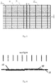
- a solar cell photovoltaic module provided by the present invention comprises, a plurality of matrix-arranged cells, as shown in Fig. 1 , a light receiving surface of each cell 10 is distributed with four longitudinal main grids 21 and 32 transverse fine grids 22, of course, the numbers of the main grids 21 and the fines grids 22 may increase or decrease according to requirement, and the present embodiment only gives an example, and the main grids 21 collect currents on the fine grids 22 connected thereto.
- the cell 10 is obtained by divided a normal cell evenly along 2 transverse parallel lines, that is, 1/3 of the normal cell, and is rectangular, wherein a length L1 of a long side thereof is 156.75 ⁇ 0.25 mm or is selected in the range of 156 - 160 mm, a length L2 of a short side thereof is 52.25 ⁇ 0.25 mm or is selected in the range of 31 - 54 mm, and the widths d of the main grids is 0.5 - 0.6 mm, and may broadened to 0.4 - 0.7 mm.
- the solar cell photovoltaic module comprises a plurality of matrix-arranged cells 10, a direction parallel to the long sides of the cells 10 is transverse, and a direction parallel to the short sides of the cells 10 is longitudinal, a transverse arrangement, i.e., a number of columns of the matrix of the cells 10 is 6, and a longitudinal arrangement, i.e., a number of rows of the matrix of the cells is 7.
- spacing G between each two adjacent cells both in the transverse direction and in the longitudinal direction is 0 - 0.5 mm.
- the currents collected by the main grids 21 are transmitted through interconnectors that connect to the main grids 21, and the interconnectors are divided into cell-to-cell interconnectors 30 and string-to-string interconnectors 33.
- each cell-to-cell interconnect 30 is a light receiving surface end 31, and the other end thereof is a back light surface end 32, as shown in Figs. 2 - 4 , the light receiving surface end 31 is directly welded to one main grid 21 of one cell 10 on the right side, the back light surface end 33 is connected to a main grid 21 of a back light surface of another cell 10 on the left side, and the cell-to-cell interconnect 30 is used to connect the two cells in series.
- the string-to-string interconnectors 33 perpendicularly intersect the cell-to-cell interconnectors 30, and the string-to-string interconnect 33 are welded on the back light surface ends 32, of course, also can be welded on the light receiving surface ends 31, in the present embodiment, material of the string-to-string interconnectors 33 uses tinned copper tapes, and the string-to-string interconnectors 33 are arranged in a density of every three rows, that is, in every other two rows.
- Widths of the cell-to-cell interconnectors 30 are in the range of 0.5 - 0.8 mm, thicknesses thereof are in the range of 0.12 - 0.18 mm; widths of the string-to-string interconnectors are in the range of 0.5 - 6 mm, thicknesses thereof are in the range of 0.1 - 0.4 mm.
- the string-to-string interconnectors 33 may also use conductive tapes or transparent conductive films, wherein transparent conductive material may interconnected on the back light surface or the light receiving surface, to avoid the influence of the shade by itself.
- conductive tapes or transparent conductive films wherein transparent conductive material may interconnected on the back light surface or the light receiving surface, to avoid the influence of the shade by itself.
- transparent conductive material may interconnected on the back light surface or the light receiving surface, to avoid the influence of the shade by itself.
- Such a design may be used in a double-sided cell, and may also be used in cell assembly applications such as no main grid process, welding strip process.
- double glass process and a narrow frame protection can be combined, to utilize the characteristics of high water resistance, such that the potential leakage of the cells 10 can be solved, and using a narrow frame protection, the convenient installation of assembly, low cost and high reliability can be achieved, especially for the technology of double-sided cells, the requirement of the front and back non-shading installation can resolved.
- the horizontal solar cell photovoltaic assembly comprises two solar cell photovoltaic modules 1 arranged side-by-side, that is, arranged along a direction of long sides of the cells 10, and bus bars 4 for collecting currents of the interconnectors, and the bus bars 4 are parallel to the long sides of the cells 10, the two solar cell photovoltaic modules 1 are connected to a virtual conductive wire 5 via diodes (not shown), and the virtual conductive wire 5 may be a conventional thin bus strip.
- the virtual conductive wire 5 and the cells 10 are isolated by insulating material.
- the insulating material may be conventional EPE material or a transparent insulating EPC or a transparent backplane, so as to ensure that the virtual conductive wire 5 does not directly contact the cells 10.
- a junction box (not shown) is connected with an output through the bus bars 4 and the virtual conductive wire 5, and here, the junction box adopts a three pin structure, and the working current of an employed single duodiode is between 15 A and 20 A.
- the solar cell photovoltaic module 1 in the present embodiment differs from that in Example 1 by that the string-to-string interconnectors 33 are arranged in a density of every two rows, that is, in every other row.
- the double-sided cell assembly uses transparent insulating conductive material and transparent conductive film material.
- the single-sided cell assembly may directly use non-transparent insulating conductive material and non-transparent conductive film material, directly arranged on the back side.
- Fig. 6 it differs from Embodiment 1 by that, in the solar cell photovoltaic module 1 is arranged side-by-side, the number of columns of the matrix of the cells 10 is 3, and the row thereof is 20.
- a vertical solar cell photovoltaic assembly is configured.
- the string-to-string interconnectors 33 are also arranged in a density of every three rows, that is, in every other two rows.
Landscapes
- Photovoltaic Devices (AREA)
Description
- The present invention relates to solar cell technical field, and particular to a solar cell photovoltaic module and a solar cell photovoltaic assembly.
- With the rise of energy prices, the development and utilization of new energy sources has become the main topic of research in the nowadays energy field. Due to that solar energy has the advantages of no pollution, no regional restrictions, inexhaustible advantages and the like, research on solar power has become the main direction for the development and utilization of new energy sources. Using solar cell to generate electricity is a major way for people to use solar energy nowadays, however, existing solar cell has the following disadvantages.
- 1. The present arrangement of the solar cells is: the spacing between cells is 2 mm, the spacing between strings is 3 mm, the entire blank area of the solar cell assembly is relatively large, and the utilization rate of power generating is low. Although a stacked cell assembly is designed, and the power is improved, the stacked cell assembly increases the usage amount of the cells, and cells of the stacked part cannot generate electricity, resulting in a significant increase in the cost of the assembly, and therefore the cost performance is not high.
- 2. The present conventional assemblies adopt full-piece welding, and the currents of the cells are relatively large, which actually causes that the internal loss of the assemblies increases exponentially, and the power cannot be increased. In order to reduce the internal loss, the interconnectors employed by the design are thickened, and correspondingly, the hidden crack preventing capability of the cells is reduced, and meanwhile the cost of assembly is increased.
- 3. The present battery mainly employs 4 main grids or 5 main grids design, and the widths of the main grids are 1.1 mm and 0.8 mm, respectively, the widths of the main grids are relatively large, which reduces the actual irradiation area of the cells and then reduces the power of the cells; although the 12-grid cell assembly is designed to reduce the widths of the main grids, this assembly has a small welding contact surface, and a high potential risk of reliability, welding strip used in the 12 grid cells is relatively thick, and at present the thickness of most of the used copper wire material is 0.39 mm, which increases by 40% compared with the conventional welding strip with a thickness of 0.27mm, and in order to reduce hidden crack, the thickness of encapsulating material has to be further increased, thus increasing the cost of the assembly. In addition, the usage amounts of the main grid material and the interconnector material actually used are large, which further increase the cost. If a rounded welding strip is used, there is still a problem that a real surface contact cannot be achieved, resulting a long-term reducing of the reliability of connections between the main grids and the copper-based material actually. The performance of the product is not improved but the risk is.
- 4. In the design of conventional assemblies, the internal circuit is a series structure formed by a plurality of cells, and if an abnormality occurs in one string, the hot spot protection is usually conducted via a diode, and the overall power generation loss relates to the entire string. During the periods of sunrise in the morning and sunset in the afternoon, it faces the waste of power generation by shade, especially the waste of high-efficiency assemblies in this aspect is higher, and therefore, in the case of frequent shade of foreign matter such as bird droppings and leaves, the lack of cleanliness in time which results in the wastage of power generating capacity is a hidden trouble seriously affecting the income of the power station.
- 5. With the further improvement of the efficiency of the cells, the efficiency of the cells has been increased to 19.5% for polycrystalline PERC of mass production, 20.8% for monocrystalline cells, 21% for N-type double-sided cells, and 22.5% for heterojunction cells on average. The operating current of the overall cells rises rapidly. With the application and attenuation, the potential suitability between the cells inside the same assembly increases, with the addition of the external shading or internal hidden cracking and the like of the potential application process, how to improve the suitability of the cells in the assembly becomes a key element of the actual long-term power generation performance. In addition, for the double-sided cell assembly, the difference in the reflective environment at the back results in very great fluctuations and differences in reflection and power generation output, which is a factor that has to face and that results in the difference in suitability of the cells of the assembly during operation.
- 6. At present, in order to solve the abnormalities such as shade of cells or hot spots inside the assembly, the process employed is that a diode is provided between a string and another string, and current shunting and abnormal cell protection are realized through reverse conduction of the diode. However, the start-up of the diode actually separates the string circuit entirely, and reduces the voltage of the entire assembly according to the configuration of the diode proportionally. A local abnormality of a single cell leads to that the entire string of cells does not provide power generation to the working circuit due to being protected by the diode. The damage to power generation capacity is multiplied based on the number of cells of protected strings. In addition, as a centralized inverter circuit, the voltage drop of a single string further affects other parallel string circuits, resulting in the influence and damage of the final output of the combiner box. In addition, there is also an intelligent optimizing chip design for the strings, which monitors the voltage and current of each string and optimizes the string through the chip. This can properly reduce the damage of the string voltage, but it is still an improvement that stays at the string level. The increased cost of string level optimization design is relatively high, and the string level optimization design does not achieve large-scale acceptance in the market in the industry.
- 7. The amount of power generated by the assembly is directly related to the temperature at which the assembly is operating. The higher the operating temperature, the less power generated by the assembly. As described in 5#, the increase of the efficiency of the cells, the raising of the current, and the operating temperature of conventional assembly actually form the restraining factors of the generating capacity. The hot spots or hidden cracking of the assembly in the work process, or the inconformity of the attenuation difference between the cells of the assembly, will lead to internal loss and temperature rise of the assembly, and eventually lead to that the power generation capacity of the assembly cannot be optimized.
- 8. The latest technology of the present assembly is the process design of the overlapped assembly product. There is no welding strip on the surface of the actual overlapped assembly, and under the condition that the cells have hidden cracks, the entire string will suffer from obstructed current output, and the risk of hot spot failure will increase. In addition, the overlapped assembly itself s the cells to overlap and connect with each other to form a circuit for current output. How to compress the inter-cell spacing to close to zero in the assembly design and to improve the conversion efficiency of the assembly, the advantages and the short boards of the overlapped assembly are obvious.
CN 206 116 415 U describes a solar cell photovoltaic module known in the prior art and such as described below in Example 1.CN 202 231 05 U describes a solar cell photovoltaic assembly, such as known in the prior art. - The present invention provides a solar cell photovoltaic assembly, to solve the above mentioned technical problems existing in the existing solar cell photovoltaic assemblies.
- To solve the above mentioned technical problems, the present invention provides a solar cell photovoltaic assembly according to
claim 1. - It should be noted that the cells can be obtained by cutting a present conventional cell, for example, dividing a conventional cell along parallel lines into 2 - 12 pieces, or directly obtaining cells of a required size through a silicon slice one-time ingot process.
- In an embodiment, spacing between each two adjacent cells is 0 - 0.5 mm.
- In an embodiment, widths of the cell-to-cell interconnectors are 0.5 - 0.8 mm, thicknesses thereof are 0.12 - 0.18 mm, and widths of the string-to-string interconnectors are 0.5 - 6 mm, thicknesses thereof are 0.1 - 0.4 mm.
- In an embodiment, the string-to-string interconnectors employ tinned copper tapes, conductive tapes or transparent conductive films.
- In an embodiment, a direction parallel to the long sides of the cells is transverse, and a direction parallel to the short sides of the cells is longitudinal, a transverse arrangement, i.e., a number of columns of the matrix-arranged cells is 2 - 6, and a longitudinal arrangement, i.e., a number of rows of the matrix-arranged cells is 5 - 40, the string-to-string interconnectors are arranged in a density of every 1 - 3 row(s) of cells.
- To prevent disconnection of the assembly and thus paralysis resulting from one module failure, in the prior art, two adjacent solar cell photovoltaic modules are generally connected via a diode or via a virtual conductive wire and a diode, and a junction box is connected with an output via the bus bars or the bus bars and the virtual conductive wire. In this way, when one module fails, the connection can through the diode or the virtual conductive wire, that is, the failure module is short-circuited, to ensure the normal operation of other modules.
- In an embodiment, the solar cell photovoltaic modules are arranged along the long sides of the cells, and the bus bars are parallel to the long sides of the cells.
- It should be noted that the direction that the long side of the assembly is parallel to the long side of the cell is horizontal, and the direction that the long side of the assembly is parallel to the short side of the cell is vertical.
-
-
Fig. 1 is a structure schematic diagram of a light receiving surface without arranging interconnectors of Example 1; -
Fig. 2 is a structure schematic diagram of a back light surface of a solar cell photovoltaic module of Example 1; -
Fig. 3 is a partial structure schematic diagram of a light receiving surface of the solar cell photovoltaic module ofFig. 2 ; -
Fig. 4 is a connection schematic diagram between cell-to-cell interconnectors and cells of Example 1; -
Fig. 5 is a structure schematic diagram of a back light surface of a horizontal type solar cell photovoltaic assembly ofEmbodiment 1; -
Fig. 6 is a structure schematic diagram of a back light surface of a vertical type solar cell photovoltaic assembly of Embodiment 2. - Wherein:
10 - cell; 21 - main grid; 22 - fine grid; 30 - cell-to-cell interconnector; 31 - light receiving surface end; 32 - back light surface end; 33 - string-to-string interconnector. - The exemplary embodiments of the present invention are explained in detail combining with the accompanying drawings so that purposes, features and advantages of the present invention can be more obvious and more understandable. It should be noted that the drawings of the present invention all adopt simplified forms and all use non-precise proportions, and are only used for the purpose of conveniently and clearly explaining the embodiments of the present invention.
- A solar cell photovoltaic module provided by the present invention comprises, a plurality of matrix-arranged cells, as shown in
Fig. 1 , a light receiving surface of eachcell 10 is distributed with four longitudinalmain grids fine grids 22, of course, the numbers of themain grids 21 and thefines grids 22 may increase or decrease according to requirement, and the present embodiment only gives an example, and themain grids 21 collect currents on thefine grids 22 connected thereto. Thecell 10 is obtained by divided a normal cell evenly along 2 transverse parallel lines, that is, 1/3 of the normal cell, and is rectangular, wherein a length L1 of a long side thereof is 156.75±0.25 mm or is selected in the range of 156 - 160 mm, a length L2 of a short side thereof is 52.25±0.25 mm or is selected in the range of 31 - 54 mm, and the widths d of the main grids is 0.5 - 0.6 mm, and may broadened to 0.4 - 0.7 mm. - As shown in
Fig. 2 , the solar cell photovoltaic module comprises a plurality of matrix-arrangedcells 10, a direction parallel to the long sides of thecells 10 is transverse, and a direction parallel to the short sides of thecells 10 is longitudinal, a transverse arrangement, i.e., a number of columns of the matrix of thecells 10 is 6, and a longitudinal arrangement, i.e., a number of rows of the matrix of the cells is 7. - As shown in
Fig. 3 , enlarging a partial 2 × 2 matrix of the cells, spacing G between each two adjacent cells both in the transverse direction and in the longitudinal direction is 0 - 0.5 mm. The currents collected by themain grids 21 are transmitted through interconnectors that connect to themain grids 21, and the interconnectors are divided into cell-to-cell interconnectors 30 and string-to-string interconnectors 33. - As shown in
Fig. 4 , an end of each cell-to-cell interconnect 30 is a light receivingsurface end 31, and the other end thereof is a backlight surface end 32, as shown inFigs. 2 - 4 , the light receivingsurface end 31 is directly welded to onemain grid 21 of onecell 10 on the right side, the backlight surface end 33 is connected to amain grid 21 of a back light surface of anothercell 10 on the left side, and the cell-to-cell interconnect 30 is used to connect the two cells in series. The string-to-string interconnectors 33 perpendicularly intersect the cell-to-cell interconnectors 30, and the string-to-string interconnect 33 are welded on the back light surface ends 32, of course, also can be welded on the light receiving surface ends 31, in the present embodiment, material of the string-to-string interconnectors 33 uses tinned copper tapes, and the string-to-string interconnectors 33 are arranged in a density of every three rows, that is, in every other two rows. - Widths of the cell-to-
cell interconnectors 30 are in the range of 0.5 - 0.8 mm, thicknesses thereof are in the range of 0.12 - 0.18 mm; widths of the string-to-string interconnectors are in the range of 0.5 - 6 mm, thicknesses thereof are in the range of 0.1 - 0.4 mm. - It should be noted that the string-to-
string interconnectors 33 may also use conductive tapes or transparent conductive films, wherein transparent conductive material may interconnected on the back light surface or the light receiving surface, to avoid the influence of the shade by itself. Such a design may be used in a double-sided cell, and may also be used in cell assembly applications such as no main grid process, welding strip process. - It should be noted that, for the encapsulation of the
cells 10 provided in the present invention, double glass process and a narrow frame protection can be combined, to utilize the characteristics of high water resistance, such that the potential leakage of thecells 10 can be solved, and using a narrow frame protection, the convenient installation of assembly, low cost and high reliability can be achieved, especially for the technology of double-sided cells, the requirement of the front and back non-shading installation can resolved. - As shown in
Fig. 5 , the horizontal solar cell photovoltaic assembly comprises two solar cellphotovoltaic modules 1 arranged side-by-side, that is, arranged along a direction of long sides of thecells 10, andbus bars 4 for collecting currents of the interconnectors, and the bus bars 4 are parallel to the long sides of thecells 10, the two solar cellphotovoltaic modules 1 are connected to a virtualconductive wire 5 via diodes (not shown), and the virtualconductive wire 5 may be a conventional thin bus strip. The virtualconductive wire 5 and thecells 10 are isolated by insulating material. The insulating material may be conventional EPE material or a transparent insulating EPC or a transparent backplane, so as to ensure that the virtualconductive wire 5 does not directly contact thecells 10. A junction box (not shown) is connected with an output through thebus bars 4 and the virtualconductive wire 5, and here, the junction box adopts a three pin structure, and the working current of an employed single duodiode is between 15 A and 20 A. - The solar cell
photovoltaic module 1 in the present embodiment differs from that in Example 1 by that the string-to-string interconnectors 33 are arranged in a density of every two rows, that is, in every other row. - It is recommended that the double-sided cell assembly uses transparent insulating conductive material and transparent conductive film material. The single-sided cell assembly may directly use non-transparent insulating conductive material and non-transparent conductive film material, directly arranged on the back side.
- As shown in
Fig. 6 , it differs fromEmbodiment 1 by that, in the solar cellphotovoltaic module 1 is arranged side-by-side, the number of columns of the matrix of thecells 10 is 3, and the row thereof is 20. A vertical solar cell photovoltaic assembly is configured. The string-to-string interconnectors 33 are also arranged in a density of every three rows, that is, in every other two rows. - It is obvious that those skilled in the art can make various changes or modifications on the present invention without depart from the scope of the present invention. Thus, the present invention is also intended to encompass these changes and modifications of the present invention which belong to the scope of the claims of the invention and equivalents thereof.
Claims (6)
- A solar cell photovoltaic assembly, comprising more than two solar cell photovoltaic modules and bus bars for collecting currents of the interconnectors (30, 33);each solar cell photovoltaic module comprising a plurality of matrix-arranged cells (10), wherein a plurality of main grids (21) and fine grids (22) are distributed on a light receiving surface of the cells (10), the main grids (21) collect currents on the fine grids (22) connected thereto, the currents collected by the main grids (21) are transmitted through interconnectors (30, 33) that connect to the main grids (21), the cells (10) are rectangular, lengths of long sides of the cells (10) are 156 - 160 mm, lengths of short sides of the cells (10) are 31 - 54 mm, and the main grids (21) are parallel to the short sides of the cells (10), and the widths of the main grids (21) are 0.4 - 0.7 mm, preferably 0.5 - 0.6 mm;is characterized in that,the interconnectors (30, 33) comprise cell-to-cell interconnectors (30) and string-to-string interconnectors (33), wherein the cell-to-cell interconnectors (30) transport currents between the cells (10) along a direction of the main grids (21), and the string-to-string interconnectors (33) connect parallel cell-to-cell interconnectors (30) in series;the cell-to-cell interconnectors (30) are arranged parallel to main grids (21), and the string-to-string interconnectors (33) perpendicularly intersect with the cell-to-cell interconnectors (30) and connect the cell-to-cell interconnectors (30) intersecting therewith in series;an end of each cell-to-cell interconnector (30) is a light receiving surface end (31), and the other end thereof is a back light surface end (32), the light receiving surface end (31) is connected to one main grid (21) of one cell (10), the back light surface end (32) is connected to a main grid (21) of a back light surface of another cell (10), the cell-to-cell interconnector (30) is used to connect two cells (10) in series, and each string-to-string interconnector (33) is welded on the back light surface end (32).
- The solar cell photovoltaic assembly according to claim 1, wherein the solar cell photovoltaic modules are arranged along the long sides of the cells (10), and the bus bars are parallel to the long sides of the cells (10).
- The solar cell photovoltaic assembly according to claim 1, wherein spacing between each two adjacent cells (10) is 0 - 0.5 mm.
- The solar cell photovoltaic assembly according to claim 1, wherein widths of the cell-to-cell interconnectors (30) are 0.5 - 0.8 mm, thicknesses thereof are 0.12 - 0.18 mm, and widths of the string-to-string interconnects (33) are 0.5 - 6 mm, thicknesses thereof are 0.1 - 0.4 mm.
- The solar cell photovoltaic assembly according to claim 1, wherein the string-to-string interconnectors (33) employ tinned copper tape, conductive tape or transparent conductive film.
- The solar cell photovoltaic assembly according to any one of claims 1 - 5, wherein a direction parallel to the long sides of the cells (10) is transverse, and a direction parallel to the short sides of the cells (10) is longitudinal, a number of columns of the matrix-arranged cells is 2 - 6, and a number of rows of the matrix-arranged cells is 5 - 40.
Applications Claiming Priority (2)
| Application Number | Priority Date | Filing Date | Title |
|---|---|---|---|
| CN201710424871.XA CN107170841B (en) | 2017-06-07 | 2017-06-07 | Solar cell photovoltaic module and solar cell photovoltaic module |
| PCT/CN2017/089372 WO2018223425A1 (en) | 2017-06-07 | 2017-06-21 | Solar cell photovoltaic module and solar cell photovoltaic array |
Publications (3)
| Publication Number | Publication Date |
|---|---|
| EP3637477A1 EP3637477A1 (en) | 2020-04-15 |
| EP3637477A4 EP3637477A4 (en) | 2021-05-19 |
| EP3637477B1 true EP3637477B1 (en) | 2022-07-13 |
Family
ID=59825444
Family Applications (1)
| Application Number | Title | Priority Date | Filing Date |
|---|---|---|---|
| EP17912708.9A Active EP3637477B1 (en) | 2017-06-07 | 2017-06-21 | Solar cell photovoltaic array |
Country Status (7)
| Country | Link |
|---|---|
| US (1) | US20190189823A1 (en) |
| EP (1) | EP3637477B1 (en) |
| JP (1) | JP6932186B2 (en) |
| CN (1) | CN107170841B (en) |
| AU (1) | AU2017417637B2 (en) |
| MY (1) | MY197283A (en) |
| WO (1) | WO2018223425A1 (en) |
Families Citing this family (19)
| Publication number | Priority date | Publication date | Assignee | Title |
|---|---|---|---|---|
| CN108022992A (en) * | 2017-12-29 | 2018-05-11 | 苏州阿特斯阳光电力科技有限公司 | Cell piece and photovoltaic module |
| CN108461577A (en) * | 2018-04-08 | 2018-08-28 | 浙江晶科能源有限公司 | A kind of production method of photovoltaic module |
| CN110768627A (en) * | 2018-07-27 | 2020-02-07 | 安世亚太科技股份有限公司 | Guardrail type photovoltaic power station |
| JP2022525929A (en) * | 2019-03-18 | 2022-05-20 | ソーラーワット リミテッド | Solar array module for power generation |
| CN110277460B (en) * | 2019-07-16 | 2024-12-10 | 无锡鼎森茂科技有限公司 | Solar cells and photovoltaic modules |
| CN110379880A (en) * | 2019-08-07 | 2019-10-25 | 常州时创能源科技有限公司 | A kind of cascaded structure of solar battery sheet |
| CN110649119B (en) * | 2019-09-12 | 2024-06-14 | 常州比太科技有限公司 | A solar power generation component based on crystalline silicon and its preparation method |
| CN110473934A (en) * | 2019-09-18 | 2019-11-19 | 苏州阿特斯阳光电力科技有限公司 | Photovoltaic module and preparation method thereof |
| CN110660874A (en) * | 2019-09-30 | 2020-01-07 | 通威太阳能(合肥)有限公司 | Auxiliary grid electrode and solar cell |
| CN110838527B (en) * | 2019-10-30 | 2024-03-08 | 江苏朗道新能源有限公司 | Cell for half-sheet shingled photovoltaic module and manufacturing method of module |
| CN110828598B (en) * | 2019-10-30 | 2024-03-08 | 江苏朗道新能源有限公司 | Half-sheet laminated tile assembly and manufacturing method thereof |
| CN114972150B (en) * | 2021-02-24 | 2023-12-05 | 正泰集团研发中心(上海)有限公司 | Method for detecting dimension defect of photovoltaic module |
| CN113471308A (en) * | 2021-08-10 | 2021-10-01 | 苏州卡睿杰新材料科技有限公司 | Main-grid-free heterojunction solar cell and laminated tile assembly prepared by same |
| CN113824401B (en) * | 2021-10-12 | 2024-03-01 | 北京朔风企业管理咨询有限公司 | New forms of energy bus stop board solar energy power generation light board detecting system |
| EP4254515B1 (en) | 2022-03-28 | 2024-08-21 | Jinko Solar (Haining) Co., Ltd. | Photovoltaic module and method for manufacturing a photovoltaic module |
| CN115207148A (en) * | 2022-03-28 | 2022-10-18 | 晶科能源(海宁)有限公司 | Photovoltaic module and preparation method |
| CN116344670A (en) * | 2023-02-27 | 2023-06-27 | 苏州赛伍应用技术股份有限公司 | A kind of method of string welding of HJT photovoltaic cell |
| US12094990B1 (en) * | 2023-03-09 | 2024-09-17 | Jinko Solar (Haining) Co., Ltd. | Photovoltaic curtain wall and method for manufacturing photovoltaic curtain wall |
| JP2026036739A (en) * | 2024-08-21 | 2026-03-06 | 唐山海泰新能科技股▲ふん▼有限公司 | Solar modules compatible with cell technology iterations |
Family Cites Families (16)
| Publication number | Priority date | Publication date | Assignee | Title |
|---|---|---|---|---|
| JP2000315811A (en) * | 1999-04-30 | 2000-11-14 | Sekisui Jushi Co Ltd | Method for connecting solar cells in series and solar cell module |
| CN101867321B (en) * | 2010-05-31 | 2013-04-03 | 江西赛维Ldk太阳能高科技有限公司 | Solar cell string and solar cell component for ground power generation and solar cell plate thereof |
| KR20110135203A (en) * | 2010-06-10 | 2011-12-16 | 삼성전자주식회사 | Solar cell module and manufacturing method thereof |
| WO2012001815A1 (en) * | 2010-07-02 | 2012-01-05 | 三菱電機株式会社 | Solar cell module and method for manufacturing same |
| CN202009010U (en) * | 2011-03-14 | 2011-10-12 | 宁波矽源达新能源有限公司 | Spliced solar polycrystalline battery piece |
| CN202231045U (en) * | 2011-10-17 | 2012-05-23 | 阿特斯(中国)投资有限公司 | solar cell module |
| US20130192657A1 (en) * | 2012-02-01 | 2013-08-01 | Tigo Energy, Inc. | Enhanced System and Method for Matrix Panel Ties for Large Installations |
| CN103367482A (en) * | 2012-04-09 | 2013-10-23 | 中电电气(上海)太阳能科技有限公司 | Photovoltaic assembly |
| JP5889738B2 (en) * | 2012-07-10 | 2016-03-22 | デクセリアルズ株式会社 | Solar cell module and manufacturing method thereof |
| US10090430B2 (en) * | 2014-05-27 | 2018-10-02 | Sunpower Corporation | System for manufacturing a shingled solar cell module |
| CN203733815U (en) * | 2014-02-26 | 2014-07-23 | 中电投西安太阳能电力有限公司 | Multi-grid solar cell assembly |
| CN204596801U (en) * | 2014-10-08 | 2015-08-26 | 上海神舟新能源发展有限公司 | A kind of N-type double-sided solar battery sheet of many main grids |
| CN104600141B (en) * | 2015-02-06 | 2018-04-03 | 协鑫集成科技股份有限公司 | Solar cell module |
| JP2017034149A (en) * | 2015-08-04 | 2017-02-09 | シャープ株式会社 | Solar cell module |
| CN106663706B (en) * | 2015-08-18 | 2019-10-08 | 太阳能公司 | Solar panel |
| CN206116415U (en) * | 2016-08-26 | 2017-04-19 | 泰州中来光电科技有限公司 | Solar cell string and subassembly and system thereof |
-
2017
- 2017-06-07 CN CN201710424871.XA patent/CN107170841B/en active Active
- 2017-06-21 WO PCT/CN2017/089372 patent/WO2018223425A1/en not_active Ceased
- 2017-06-21 US US16/330,750 patent/US20190189823A1/en not_active Abandoned
- 2017-06-21 AU AU2017417637A patent/AU2017417637B2/en active Active
- 2017-06-21 MY MYPI2019001966A patent/MY197283A/en unknown
- 2017-06-21 EP EP17912708.9A patent/EP3637477B1/en active Active
- 2017-06-21 JP JP2019517249A patent/JP6932186B2/en active Active
Also Published As
| Publication number | Publication date |
|---|---|
| EP3637477A1 (en) | 2020-04-15 |
| EP3637477A4 (en) | 2021-05-19 |
| US20190189823A1 (en) | 2019-06-20 |
| BR112019006119A2 (en) | 2020-02-04 |
| CN107170841B (en) | 2021-01-22 |
| CN107170841A (en) | 2017-09-15 |
| MY197283A (en) | 2023-06-09 |
| JP2020501333A (en) | 2020-01-16 |
| AU2017417637B2 (en) | 2020-05-21 |
| WO2018223425A1 (en) | 2018-12-13 |
| JP6932186B2 (en) | 2021-09-08 |
| AU2017417637A1 (en) | 2019-03-28 |
Similar Documents
| Publication | Publication Date | Title |
|---|---|---|
| EP3637477B1 (en) | Solar cell photovoltaic array | |
| CN204538036U (en) | Solar panel, solar cell, solar cell panel assembly and solar battery apparatus | |
| EP3985742B1 (en) | Hot-spot-resistant single-plate photovoltaic module | |
| EP3306675A1 (en) | Cell module using back contact process and manufacturing method therefor | |
| CN206711906U (en) | A kind of solar cell module and solar panel | |
| CN107946392A (en) | A kind of intelligence heat resistanceheat resistant spot photovoltaic module | |
| CN110783415A (en) | Novel solar cell module and preparation method thereof | |
| CN114927591A (en) | Photovoltaic module | |
| CN106876486A (en) | The group string attachment structure of P-type crystal silicon back contacts double-side cell, component and method | |
| CN207320133U (en) | A kind of stacked solar cell module | |
| CN212085018U (en) | Shingled photovoltaic module | |
| CN105830230B (en) | A kind of back contacts technique battery component and preparation method thereof | |
| CN209822663U (en) | Heat spot-resistant single-plate photovoltaic module | |
| CN110649119B (en) | A solar power generation component based on crystalline silicon and its preparation method | |
| CN209561427U (en) | Photovoltaic modules | |
| CN103022171A (en) | Solar cell photovoltaic module | |
| CN207587743U (en) | Solar cell photovoltaic module and solar cell photovoltaic component | |
| CN216648328U (en) | Heterojunction battery assembly | |
| CN108336163B (en) | P-type double-sided solar cell module | |
| CN211789055U (en) | High-power non-hot spot effect assembly | |
| CN214068739U (en) | Laminated photovoltaic module with directly parallel-connected battery strings | |
| CN214068735U (en) | Photovoltaic module cell piece with same-plane equal-potential parallel connection | |
| CN111446322B (en) | A high power component without hot spot effect | |
| CN114759109A (en) | Laminated solar module | |
| CN223816363U (en) | Back contact solar cell module structure with low hot spot temperature |
Legal Events
| Date | Code | Title | Description |
|---|---|---|---|
| STAA | Information on the status of an ep patent application or granted ep patent |
Free format text: STATUS: THE INTERNATIONAL PUBLICATION HAS BEEN MADE |
|
| PUAI | Public reference made under article 153(3) epc to a published international application that has entered the european phase |
Free format text: ORIGINAL CODE: 0009012 |
|
| STAA | Information on the status of an ep patent application or granted ep patent |
Free format text: STATUS: REQUEST FOR EXAMINATION WAS MADE |
|
| 17P | Request for examination filed |
Effective date: 20190228 |
|
| AK | Designated contracting states |
Kind code of ref document: A1 Designated state(s): AL AT BE BG CH CY CZ DE DK EE ES FI FR GB GR HR HU IE IS IT LI LT LU LV MC MK MT NL NO PL PT RO RS SE SI SK SM TR |
|
| AX | Request for extension of the european patent |
Extension state: BA ME |
|
| DAV | Request for validation of the european patent (deleted) | ||
| DAX | Request for extension of the european patent (deleted) | ||
| A4 | Supplementary search report drawn up and despatched |
Effective date: 20210421 |
|
| RIC1 | Information provided on ipc code assigned before grant |
Ipc: H01L 31/0224 20060101AFI20210415BHEP |
|
| REG | Reference to a national code |
Ref country code: DE Ref legal event code: R079 Ref document number: 602017059549 Country of ref document: DE Free format text: PREVIOUS MAIN CLASS: H01L0031022400 Ipc: H01L0031050000 |
|
| RIC1 | Information provided on ipc code assigned before grant |
Ipc: H01L 31/068 20120101ALI20211230BHEP Ipc: H01L 31/0224 20060101ALI20211230BHEP Ipc: H01L 31/05 20140101AFI20211230BHEP |
|
| GRAP | Despatch of communication of intention to grant a patent |
Free format text: ORIGINAL CODE: EPIDOSNIGR1 |
|
| STAA | Information on the status of an ep patent application or granted ep patent |
Free format text: STATUS: GRANT OF PATENT IS INTENDED |
|
| INTG | Intention to grant announced |
Effective date: 20220208 |
|
| GRAS | Grant fee paid |
Free format text: ORIGINAL CODE: EPIDOSNIGR3 |
|
| GRAA | (expected) grant |
Free format text: ORIGINAL CODE: 0009210 |
|
| STAA | Information on the status of an ep patent application or granted ep patent |
Free format text: STATUS: THE PATENT HAS BEEN GRANTED |
|
| AK | Designated contracting states |
Kind code of ref document: B1 Designated state(s): AL AT BE BG CH CY CZ DE DK EE ES FI FR GB GR HR HU IE IS IT LI LT LU LV MC MK MT NL NO PL PT RO RS SE SI SK SM TR |
|
| REG | Reference to a national code |
Ref country code: CH Ref legal event code: EP |
|
| REG | Reference to a national code |
Ref country code: DE Ref legal event code: R096 Ref document number: 602017059549 Country of ref document: DE |
|
| REG | Reference to a national code |
Ref country code: AT Ref legal event code: REF Ref document number: 1504725 Country of ref document: AT Kind code of ref document: T Effective date: 20220815 |
|
| REG | Reference to a national code |
Ref country code: IE Ref legal event code: FG4D |
|
| REG | Reference to a national code |
Ref country code: LT Ref legal event code: MG9D |
|
| REG | Reference to a national code |
Ref country code: NL Ref legal event code: MP Effective date: 20220713 |
|
| PG25 | Lapsed in a contracting state [announced via postgrant information from national office to epo] |
Ref country code: SE Free format text: LAPSE BECAUSE OF FAILURE TO SUBMIT A TRANSLATION OF THE DESCRIPTION OR TO PAY THE FEE WITHIN THE PRESCRIBED TIME-LIMIT Effective date: 20220713 Ref country code: RS Free format text: LAPSE BECAUSE OF FAILURE TO SUBMIT A TRANSLATION OF THE DESCRIPTION OR TO PAY THE FEE WITHIN THE PRESCRIBED TIME-LIMIT Effective date: 20220713 Ref country code: PT Free format text: LAPSE BECAUSE OF FAILURE TO SUBMIT A TRANSLATION OF THE DESCRIPTION OR TO PAY THE FEE WITHIN THE PRESCRIBED TIME-LIMIT Effective date: 20221114 Ref country code: NO Free format text: LAPSE BECAUSE OF FAILURE TO SUBMIT A TRANSLATION OF THE DESCRIPTION OR TO PAY THE FEE WITHIN THE PRESCRIBED TIME-LIMIT Effective date: 20221013 Ref country code: NL Free format text: LAPSE BECAUSE OF FAILURE TO SUBMIT A TRANSLATION OF THE DESCRIPTION OR TO PAY THE FEE WITHIN THE PRESCRIBED TIME-LIMIT Effective date: 20220713 Ref country code: LV Free format text: LAPSE BECAUSE OF FAILURE TO SUBMIT A TRANSLATION OF THE DESCRIPTION OR TO PAY THE FEE WITHIN THE PRESCRIBED TIME-LIMIT Effective date: 20220713 Ref country code: LT Free format text: LAPSE BECAUSE OF FAILURE TO SUBMIT A TRANSLATION OF THE DESCRIPTION OR TO PAY THE FEE WITHIN THE PRESCRIBED TIME-LIMIT Effective date: 20220713 Ref country code: FI Free format text: LAPSE BECAUSE OF FAILURE TO SUBMIT A TRANSLATION OF THE DESCRIPTION OR TO PAY THE FEE WITHIN THE PRESCRIBED TIME-LIMIT Effective date: 20220713 Ref country code: ES Free format text: LAPSE BECAUSE OF FAILURE TO SUBMIT A TRANSLATION OF THE DESCRIPTION OR TO PAY THE FEE WITHIN THE PRESCRIBED TIME-LIMIT Effective date: 20220713 |
|
| REG | Reference to a national code |
Ref country code: AT Ref legal event code: MK05 Ref document number: 1504725 Country of ref document: AT Kind code of ref document: T Effective date: 20220713 |
|
| PG25 | Lapsed in a contracting state [announced via postgrant information from national office to epo] |
Ref country code: PL Free format text: LAPSE BECAUSE OF FAILURE TO SUBMIT A TRANSLATION OF THE DESCRIPTION OR TO PAY THE FEE WITHIN THE PRESCRIBED TIME-LIMIT Effective date: 20220713 Ref country code: IS Free format text: LAPSE BECAUSE OF FAILURE TO SUBMIT A TRANSLATION OF THE DESCRIPTION OR TO PAY THE FEE WITHIN THE PRESCRIBED TIME-LIMIT Effective date: 20221113 Ref country code: HR Free format text: LAPSE BECAUSE OF FAILURE TO SUBMIT A TRANSLATION OF THE DESCRIPTION OR TO PAY THE FEE WITHIN THE PRESCRIBED TIME-LIMIT Effective date: 20220713 Ref country code: GR Free format text: LAPSE BECAUSE OF FAILURE TO SUBMIT A TRANSLATION OF THE DESCRIPTION OR TO PAY THE FEE WITHIN THE PRESCRIBED TIME-LIMIT Effective date: 20221014 |
|
| REG | Reference to a national code |
Ref country code: DE Ref legal event code: R097 Ref document number: 602017059549 Country of ref document: DE |
|
| PG25 | Lapsed in a contracting state [announced via postgrant information from national office to epo] |
Ref country code: SM Free format text: LAPSE BECAUSE OF FAILURE TO SUBMIT A TRANSLATION OF THE DESCRIPTION OR TO PAY THE FEE WITHIN THE PRESCRIBED TIME-LIMIT Effective date: 20220713 Ref country code: RO Free format text: LAPSE BECAUSE OF FAILURE TO SUBMIT A TRANSLATION OF THE DESCRIPTION OR TO PAY THE FEE WITHIN THE PRESCRIBED TIME-LIMIT Effective date: 20220713 Ref country code: DK Free format text: LAPSE BECAUSE OF FAILURE TO SUBMIT A TRANSLATION OF THE DESCRIPTION OR TO PAY THE FEE WITHIN THE PRESCRIBED TIME-LIMIT Effective date: 20220713 Ref country code: CZ Free format text: LAPSE BECAUSE OF FAILURE TO SUBMIT A TRANSLATION OF THE DESCRIPTION OR TO PAY THE FEE WITHIN THE PRESCRIBED TIME-LIMIT Effective date: 20220713 Ref country code: AT Free format text: LAPSE BECAUSE OF FAILURE TO SUBMIT A TRANSLATION OF THE DESCRIPTION OR TO PAY THE FEE WITHIN THE PRESCRIBED TIME-LIMIT Effective date: 20220713 |
|
| PLBE | No opposition filed within time limit |
Free format text: ORIGINAL CODE: 0009261 |
|
| STAA | Information on the status of an ep patent application or granted ep patent |
Free format text: STATUS: NO OPPOSITION FILED WITHIN TIME LIMIT |
|
| PG25 | Lapsed in a contracting state [announced via postgrant information from national office to epo] |
Ref country code: SK Free format text: LAPSE BECAUSE OF FAILURE TO SUBMIT A TRANSLATION OF THE DESCRIPTION OR TO PAY THE FEE WITHIN THE PRESCRIBED TIME-LIMIT Effective date: 20220713 Ref country code: EE Free format text: LAPSE BECAUSE OF FAILURE TO SUBMIT A TRANSLATION OF THE DESCRIPTION OR TO PAY THE FEE WITHIN THE PRESCRIBED TIME-LIMIT Effective date: 20220713 |
|
| 26N | No opposition filed |
Effective date: 20230414 |
|
| PG25 | Lapsed in a contracting state [announced via postgrant information from national office to epo] |
Ref country code: AL Free format text: LAPSE BECAUSE OF FAILURE TO SUBMIT A TRANSLATION OF THE DESCRIPTION OR TO PAY THE FEE WITHIN THE PRESCRIBED TIME-LIMIT Effective date: 20220713 |
|
| PG25 | Lapsed in a contracting state [announced via postgrant information from national office to epo] |
Ref country code: SI Free format text: LAPSE BECAUSE OF FAILURE TO SUBMIT A TRANSLATION OF THE DESCRIPTION OR TO PAY THE FEE WITHIN THE PRESCRIBED TIME-LIMIT Effective date: 20220713 |
|
| PG25 | Lapsed in a contracting state [announced via postgrant information from national office to epo] |
Ref country code: MC Free format text: LAPSE BECAUSE OF FAILURE TO SUBMIT A TRANSLATION OF THE DESCRIPTION OR TO PAY THE FEE WITHIN THE PRESCRIBED TIME-LIMIT Effective date: 20220713 |
|
| PG25 | Lapsed in a contracting state [announced via postgrant information from national office to epo] |
Ref country code: MC Free format text: LAPSE BECAUSE OF FAILURE TO SUBMIT A TRANSLATION OF THE DESCRIPTION OR TO PAY THE FEE WITHIN THE PRESCRIBED TIME-LIMIT Effective date: 20220713 |
|
| REG | Reference to a national code |
Ref country code: CH Ref legal event code: PL |
|
| REG | Reference to a national code |
Ref country code: BE Ref legal event code: MM Effective date: 20230630 |
|
| PG25 | Lapsed in a contracting state [announced via postgrant information from national office to epo] |
Ref country code: LU Free format text: LAPSE BECAUSE OF NON-PAYMENT OF DUE FEES Effective date: 20230621 |
|
| REG | Reference to a national code |
Ref country code: IE Ref legal event code: MM4A |
|
| PG25 | Lapsed in a contracting state [announced via postgrant information from national office to epo] |
Ref country code: LU Free format text: LAPSE BECAUSE OF NON-PAYMENT OF DUE FEES Effective date: 20230621 |
|
| PG25 | Lapsed in a contracting state [announced via postgrant information from national office to epo] |
Ref country code: IE Free format text: LAPSE BECAUSE OF NON-PAYMENT OF DUE FEES Effective date: 20230621 |
|
| PG25 | Lapsed in a contracting state [announced via postgrant information from national office to epo] |
Ref country code: IE Free format text: LAPSE BECAUSE OF NON-PAYMENT OF DUE FEES Effective date: 20230621 Ref country code: CH Free format text: LAPSE BECAUSE OF NON-PAYMENT OF DUE FEES Effective date: 20230630 |
|
| PG25 | Lapsed in a contracting state [announced via postgrant information from national office to epo] |
Ref country code: BE Free format text: LAPSE BECAUSE OF NON-PAYMENT OF DUE FEES Effective date: 20230630 |
|
| PG25 | Lapsed in a contracting state [announced via postgrant information from national office to epo] |
Ref country code: BG Free format text: LAPSE BECAUSE OF FAILURE TO SUBMIT A TRANSLATION OF THE DESCRIPTION OR TO PAY THE FEE WITHIN THE PRESCRIBED TIME-LIMIT Effective date: 20220713 |
|
| REG | Reference to a national code |
Ref country code: DE Ref legal event code: R079 Ref document number: 602017059549 Country of ref document: DE Free format text: PREVIOUS MAIN CLASS: H01L0031050000 Ipc: H10F0019900000 |
|
| PG25 | Lapsed in a contracting state [announced via postgrant information from national office to epo] |
Ref country code: BG Free format text: LAPSE BECAUSE OF FAILURE TO SUBMIT A TRANSLATION OF THE DESCRIPTION OR TO PAY THE FEE WITHIN THE PRESCRIBED TIME-LIMIT Effective date: 20220713 |
|
| PGFP | Annual fee paid to national office [announced via postgrant information from national office to epo] |
Ref country code: DE Payment date: 20250617 Year of fee payment: 9 |
|
| PGFP | Annual fee paid to national office [announced via postgrant information from national office to epo] |
Ref country code: GB Payment date: 20250625 Year of fee payment: 9 |
|
| PGFP | Annual fee paid to national office [announced via postgrant information from national office to epo] |
Ref country code: FR Payment date: 20250630 Year of fee payment: 9 |
|
| PG25 | Lapsed in a contracting state [announced via postgrant information from national office to epo] |
Ref country code: CY Free format text: LAPSE BECAUSE OF FAILURE TO SUBMIT A TRANSLATION OF THE DESCRIPTION OR TO PAY THE FEE WITHIN THE PRESCRIBED TIME-LIMIT; INVALID AB INITIO Effective date: 20170621 |
|
| PG25 | Lapsed in a contracting state [announced via postgrant information from national office to epo] |
Ref country code: HU Free format text: LAPSE BECAUSE OF FAILURE TO SUBMIT A TRANSLATION OF THE DESCRIPTION OR TO PAY THE FEE WITHIN THE PRESCRIBED TIME-LIMIT; INVALID AB INITIO Effective date: 20170621 |
|
| PGFP | Annual fee paid to national office [announced via postgrant information from national office to epo] |
Ref country code: IT Payment date: 20250606 Year of fee payment: 9 |
|
| PG25 | Lapsed in a contracting state [announced via postgrant information from national office to epo] |
Ref country code: TR Free format text: LAPSE BECAUSE OF FAILURE TO SUBMIT A TRANSLATION OF THE DESCRIPTION OR TO PAY THE FEE WITHIN THE PRESCRIBED TIME-LIMIT Effective date: 20220713 |