EP3637461A1 - Power electronic module - Google Patents
Power electronic module Download PDFInfo
- Publication number
- EP3637461A1 EP3637461A1 EP18199846.9A EP18199846A EP3637461A1 EP 3637461 A1 EP3637461 A1 EP 3637461A1 EP 18199846 A EP18199846 A EP 18199846A EP 3637461 A1 EP3637461 A1 EP 3637461A1
- Authority
- EP
- European Patent Office
- Prior art keywords
- power electronic
- electronic component
- semiconductor chips
- thermal insulator
- housing
- Prior art date
- Legal status (The legal status is an assumption and is not a legal conclusion. Google has not performed a legal analysis and makes no representation as to the accuracy of the status listed.)
- Granted
Links
Images


Classifications
-
- H—ELECTRICITY
- H10—SEMICONDUCTOR DEVICES; ELECTRIC SOLID-STATE DEVICES NOT OTHERWISE PROVIDED FOR
- H10W—GENERIC PACKAGES, INTERCONNECTIONS, CONNECTORS OR OTHER CONSTRUCTIONAL DETAILS OF DEVICES COVERED BY CLASS H10
- H10W40/00—Arrangements for thermal protection or thermal control
- H10W40/20—Arrangements for cooling
- H10W40/22—Arrangements for cooling characterised by their shape, e.g. having conical or cylindrical projections
- H10W40/226—Arrangements for cooling characterised by their shape, e.g. having conical or cylindrical projections characterised by projecting parts, e.g. fins to increase surface area
- H10W40/228—Arrangements for cooling characterised by their shape, e.g. having conical or cylindrical projections characterised by projecting parts, e.g. fins to increase surface area the projecting parts being wire-shaped or pin-shaped
-
- H—ELECTRICITY
- H10—SEMICONDUCTOR DEVICES; ELECTRIC SOLID-STATE DEVICES NOT OTHERWISE PROVIDED FOR
- H10W—GENERIC PACKAGES, INTERCONNECTIONS, CONNECTORS OR OTHER CONSTRUCTIONAL DETAILS OF DEVICES COVERED BY CLASS H10
- H10W40/00—Arrangements for thermal protection or thermal control
-
- H—ELECTRICITY
- H05—ELECTRIC TECHNIQUES NOT OTHERWISE PROVIDED FOR
- H05K—PRINTED CIRCUITS; CASINGS OR CONSTRUCTIONAL DETAILS OF ELECTRIC APPARATUS; MANUFACTURE OF ASSEMBLAGES OF ELECTRICAL COMPONENTS
- H05K7/00—Constructional details common to different types of electric apparatus
- H05K7/20—Modifications to facilitate cooling, ventilating, or heating
- H05K7/2039—Modifications to facilitate cooling, ventilating, or heating characterised by the heat transfer by conduction from the heat generating element to a dissipating body
-
- H—ELECTRICITY
- H05—ELECTRIC TECHNIQUES NOT OTHERWISE PROVIDED FOR
- H05K—PRINTED CIRCUITS; CASINGS OR CONSTRUCTIONAL DETAILS OF ELECTRIC APPARATUS; MANUFACTURE OF ASSEMBLAGES OF ELECTRICAL COMPONENTS
- H05K7/00—Constructional details common to different types of electric apparatus
- H05K7/20—Modifications to facilitate cooling, ventilating, or heating
- H05K7/2089—Modifications to facilitate cooling, ventilating, or heating for power electronics, e.g. for inverters for controlling motor
- H05K7/209—Heat transfer by conduction from internal heat source to heat radiating structure
-
- H—ELECTRICITY
- H10—SEMICONDUCTOR DEVICES; ELECTRIC SOLID-STATE DEVICES NOT OTHERWISE PROVIDED FOR
- H10W—GENERIC PACKAGES, INTERCONNECTIONS, CONNECTORS OR OTHER CONSTRUCTIONAL DETAILS OF DEVICES COVERED BY CLASS H10
- H10W40/00—Arrangements for thermal protection or thermal control
- H10W40/20—Arrangements for cooling
- H10W40/25—Arrangements for cooling characterised by their materials
- H10W40/257—Arrangements for cooling characterised by their materials having a heterogeneous or anisotropic structure, e.g. powder or fibres in a matrix, wire mesh or porous structures
-
- H—ELECTRICITY
- H10—SEMICONDUCTOR DEVICES; ELECTRIC SOLID-STATE DEVICES NOT OTHERWISE PROVIDED FOR
- H10W—GENERIC PACKAGES, INTERCONNECTIONS, CONNECTORS OR OTHER CONSTRUCTIONAL DETAILS OF DEVICES COVERED BY CLASS H10
- H10W74/00—Encapsulations, e.g. protective coatings
- H10W74/10—Encapsulations, e.g. protective coatings characterised by their shape or disposition
- H10W74/111—Encapsulations, e.g. protective coatings characterised by their shape or disposition the semiconductor body being completely enclosed
- H10W74/114—Encapsulations, e.g. protective coatings characterised by their shape or disposition the semiconductor body being completely enclosed by a substrate and the encapsulations
-
- H—ELECTRICITY
- H10—SEMICONDUCTOR DEVICES; ELECTRIC SOLID-STATE DEVICES NOT OTHERWISE PROVIDED FOR
- H10W—GENERIC PACKAGES, INTERCONNECTIONS, CONNECTORS OR OTHER CONSTRUCTIONAL DETAILS OF DEVICES COVERED BY CLASS H10
- H10W90/00—Package configurations
-
- H—ELECTRICITY
- H10—SEMICONDUCTOR DEVICES; ELECTRIC SOLID-STATE DEVICES NOT OTHERWISE PROVIDED FOR
- H10W—GENERIC PACKAGES, INTERCONNECTIONS, CONNECTORS OR OTHER CONSTRUCTIONAL DETAILS OF DEVICES COVERED BY CLASS H10
- H10W40/00—Arrangements for thermal protection or thermal control
- H10W40/20—Arrangements for cooling
- H10W40/22—Arrangements for cooling characterised by their shape, e.g. having conical or cylindrical projections
-
- H—ELECTRICITY
- H10—SEMICONDUCTOR DEVICES; ELECTRIC SOLID-STATE DEVICES NOT OTHERWISE PROVIDED FOR
- H10W—GENERIC PACKAGES, INTERCONNECTIONS, CONNECTORS OR OTHER CONSTRUCTIONAL DETAILS OF DEVICES COVERED BY CLASS H10
- H10W40/00—Arrangements for thermal protection or thermal control
- H10W40/20—Arrangements for cooling
- H10W40/25—Arrangements for cooling characterised by their materials
- H10W40/255—Arrangements for cooling characterised by their materials having a laminate or multilayered structure, e.g. direct bond copper [DBC] ceramic substrates
-
- H—ELECTRICITY
- H10—SEMICONDUCTOR DEVICES; ELECTRIC SOLID-STATE DEVICES NOT OTHERWISE PROVIDED FOR
- H10W—GENERIC PACKAGES, INTERCONNECTIONS, CONNECTORS OR OTHER CONSTRUCTIONAL DETAILS OF DEVICES COVERED BY CLASS H10
- H10W72/00—Interconnections or connectors in packages
- H10W72/30—Die-attach connectors
- H10W72/351—Materials of die-attach connectors
- H10W72/352—Materials of die-attach connectors comprising metals or metalloids, e.g. solders
-
- H—ELECTRICITY
- H10—SEMICONDUCTOR DEVICES; ELECTRIC SOLID-STATE DEVICES NOT OTHERWISE PROVIDED FOR
- H10W—GENERIC PACKAGES, INTERCONNECTIONS, CONNECTORS OR OTHER CONSTRUCTIONAL DETAILS OF DEVICES COVERED BY CLASS H10
- H10W90/00—Package configurations
- H10W90/701—Package configurations characterised by the relative positions of pads or connectors relative to package parts
- H10W90/731—Package configurations characterised by the relative positions of pads or connectors relative to package parts of die-attach connectors
- H10W90/734—Package configurations characterised by the relative positions of pads or connectors relative to package parts of die-attach connectors between a chip and a stacked insulating package substrate, interposer or RDL
Definitions
- the present invention relates to power electronics, and specifically to power electronic component or power electronic modules.
- Power electronic components and power electronic modules produce heat when they are operated.
- Typical power electronic components include diodes, transistors, IGBTs and thyristors.
- Typical power electronic modules comprise multiple of power electronic components which are wired together internally and function as a building blocks for certain electrical devices.
- a power electronic module may be, for example, internally wired to form an inverter bridge.
- the heat in power electronic components and power electronics modules is generated mainly during the switching instants of the components when the components are turned on or off.
- the amount of dissipated power can be up to hundreds of Watts and even over thousand watts.
- the losses that generate heat are formed in diode and transistor semiconductor chips which have an area of few square centimetres.
- the loss density can thus be over 100 Watts per square centimetre and the temperature of the chips may rise up to 175 degrees Celsius during use.
- the power electronic modules are structured such that the dissipated heat is transferred through a base plate of the module to an external heatsink which is attached firmly to the base plate.
- Power electronic modules may also be structured without a baseplate in which case the bottom of the mode is attached to a heat sink. Whether the power electronic module has a base plate or not, a heatsink is used and the power electronic module has a surface which is intended to be attached against a heatsink. The transfer of heat of a power electronic module to a heatsink is increased with a thermal interface material layer which is placed between the surface of the power electronic module and the heat sink.
- the heat transfer path from the semiconductor chip to the bottom surface of the power electronic module is designed to be effective such that as much heat is transferred through this path to the heat sink. Although most of the heat is transferred to the bottom of the module, a certain part of the dissipated heat is transferred elsewhere in the module. This heat transfers trough structural elements, such as plastic construction parts and electrically controlling pins to other parts of the structure of the module.
- the heat is transferred also to the housing of the power electronic module and further from the housing to a control board which is used for providing required control voltages to the components of the module.
- the control board increases, the reliability of the control board weakens. The increased temperature may lead to shortened lifetime of the control board and to malfunctions in the control board.
- the components of the driver card may have to be selected to withstand higher temperatures which increases the costs of the driver card.
- An object of the present invention is to provide a power electronic component to solve the above problem.
- the object of the invention is achieved by a power electronic component which is characterized by what is stated in the independent claim.
- the preferred embodiments of the invention are disclosed in the dependent claims.
- the invention is based on the idea of providing thermally insulating material to a power electronic component such that the heat transfer outside the component is limited from the areas in which the heat could damage or harm other electric components.
- An advantage of the power electronic component of the invention is that the generated heat of the power semiconductor component is not able to warm excessively other electronic components or circuits which are placed in close vicinity of the power electronic component. Further, the power electronic component of the invention is advantageous in high IP-class devices in which the heat inside an enclosure of the device is problematic. This advantageous feature is based on the fact that with the component of the present invention heat is transferred more effectively to the bottom surface of the component from which the heat can be transferred outside the enclosure.
- the invention allows increasing the integration degree of the power electronic semiconductor chips when the heat transfer from the bottom surface of the power semiconductor component is increased.
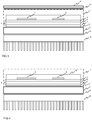
- Figure 1 shows a cross section of a known power electronic component and more specifically a power electronic component having multiple of power electronic semiconductor chips.
- a component is typically referred to as a power electronic module.
- the power electronic component is described in connection with a power electronic module.
- the power electronic component of the invention may comprise only one power electronic semiconductor chip.
- the power electronic component further comprises one or more power electronic semiconductor chips 3 mounted on a substrate 4 above the bottom surface.
- the cross section of Figure 2 shows two semiconductor chips 3 and the power electronic component is thus a power electronic module.
- a housing 2 encloses the one or more power electronic semiconductor chips.
- the power electronic component comprises a thermal insulator 21 disposed above the one or more power electronic semiconductor chips.
- the thermal insulator is above the one or more power electronic semiconductor chips as the bottom surface of the power electronic component and the thermal insulator are on the opposite sides of the one or more power electronic semiconductor chips and on the opposite sides of the substrate 4.
- the thermal insulator 21 is adapted to increase the thermal resistance from the semiconductor chips 3 towards the top of the module.
- the top of the module is defined as the surface of the housing that forms the outer surface of the module.
- the power electronic component comprises a layer of silicone gel 10 on top of the one or more power electronic semiconductor chips and the thermal insulator is arranged above the layer of silicone gel inside the housing 2.
- the term above should be understood such that the base plate is in the bottom, and the direction “up” refers to the direction from the base plate towards the housing of the power electronic component.
- the thermal insulator blocks effectively the heat transfer from the chips towards the top of the housing.
- the thermal insulator 31 is arranged on top of the housing of the semiconductor component.
- the thermal insulator 31 blocks the heat from the power semiconductor component such that a board 32 with electrical components is not heated excessively.
- Figure 3 shows a control board 32 or similar board with electrical circuits attached on the top of the housing 2. It is often desirable to have electronic circuits close to the power electronic component when the electronic circuit is used for controlling the one or more switches of the power electronic component.
- the other structural parts correspond to those of Figure 2 and the numbering of the parts correspond to Figure 2 .
- the thermal insulator is in a form of a fabric.
- the fabric comprises silicon oxide particles which are effective insulators. When the insulator is in form of a fabric, it can be cut to shape and installed in desired locations.
- the silicon oxide particles are preferably micro or nano sized and porous particles.
- An example of a suitable silicon oxide is aerogel which is known to have good thermal properties and electrical resistivity. Silicon oxide can be arranged in a fabric and thus such a fabric has a low thermal conductivity and high electrical resistance.
- Figure 5 shows another embodiment of the invention, in which the housing 51 of the power electronic component comprises plastic material with silicon oxide particles and the housing forms the thermal insulator. Silicon oxide particles can be doped in polymers such that a plastic composite is formed which is efficient both as thermal and electrical insulator.
- the plastic composite can be die casted and the housing can be formed by die casting.
- One suitable type of silicon oxide usable in the plastic material is aerogel. To avoid repetition, corresponding structural parts of Figure 5 are numbered as in the previous Figures.
- the bottom surface of the power electronic component is formed of a base plate which is internally connected to the substrate. That is, in the examples the base plate is part of the components.
- the invention is applicable also to power electronic components in which the bottom surface is formed of the surface of the substrate, i.e. components which do not have a base plate. When the component does not have a base plate, the heat is conducted from the substrate directly to a heatsink.
Landscapes
- Engineering & Computer Science (AREA)
- Microelectronics & Electronic Packaging (AREA)
- Physics & Mathematics (AREA)
- Thermal Sciences (AREA)
- Cooling Or The Like Of Semiconductors Or Solid State Devices (AREA)
Abstract
Description
- The present invention relates to power electronics, and specifically to power electronic component or power electronic modules.
- Power electronic components and power electronic modules produce heat when they are operated. Typical power electronic components include diodes, transistors, IGBTs and thyristors. Typical power electronic modules comprise multiple of power electronic components which are wired together internally and function as a building blocks for certain electrical devices. A power electronic module may be, for example, internally wired to form an inverter bridge.
- The heat in power electronic components and power electronics modules is generated mainly during the switching instants of the components when the components are turned on or off. The amount of dissipated power can be up to hundreds of Watts and even over thousand watts.
- The losses that generate heat are formed in diode and transistor semiconductor chips which have an area of few square centimetres. The loss density can thus be over 100 Watts per square centimetre and the temperature of the chips may rise up to 175 degrees Celsius during use.
- The power electronic modules are structured such that the dissipated heat is transferred through a base plate of the module to an external heatsink which is attached firmly to the base plate. Power electronic modules may also be structured without a baseplate in which case the bottom of the mode is attached to a heat sink. Whether the power electronic module has a base plate or not, a heatsink is used and the power electronic module has a surface which is intended to be attached against a heatsink. The transfer of heat of a power electronic module to a heatsink is increased with a thermal interface material layer which is placed between the surface of the power electronic module and the heat sink.
- The heat transfer path from the semiconductor chip to the bottom surface of the power electronic module is designed to be effective such that as much heat is transferred through this path to the heat sink. Although most of the heat is transferred to the bottom of the module, a certain part of the dissipated heat is transferred elsewhere in the module. This heat transfers trough structural elements, such as plastic construction parts and electrically controlling pins to other parts of the structure of the module. The heat is transferred also to the housing of the power electronic module and further from the housing to a control board which is used for providing required control voltages to the components of the module. When the temperature of the control board increases, the reliability of the control board weakens. The increased temperature may lead to shortened lifetime of the control board and to malfunctions in the control board. Further, the components of the driver card may have to be selected to withstand higher temperatures which increases the costs of the driver card.
- An object of the present invention is to provide a power electronic component to solve the above problem. The object of the invention is achieved by a power electronic component which is characterized by what is stated in the independent claim. The preferred embodiments of the invention are disclosed in the dependent claims.
- The invention is based on the idea of providing thermally insulating material to a power electronic component such that the heat transfer outside the component is limited from the areas in which the heat could damage or harm other electric components.
- An advantage of the power electronic component of the invention is that the generated heat of the power semiconductor component is not able to warm excessively other electronic components or circuits which are placed in close vicinity of the power electronic component. Further, the power electronic component of the invention is advantageous in high IP-class devices in which the heat inside an enclosure of the device is problematic. This advantageous feature is based on the fact that with the component of the present invention heat is transferred more effectively to the bottom surface of the component from which the heat can be transferred outside the enclosure.
- Further, the invention allows increasing the integration degree of the power electronic semiconductor chips when the heat transfer from the bottom surface of the power semiconductor component is increased.
- In the following the invention will be described in greater detail by means of preferred embodiments with reference to the attached drawings, in which
-
Figure 1 is shows an example of a cross section of a known power electronic module; -
Figures 2 ,3 ,4 and5 show cross sections of different embodiments of the invention. -
Figure 1 shows a cross section of a known power electronic component and more specifically a power electronic component having multiple of power electronic semiconductor chips. Such a component is typically referred to as a power electronic module. In the following description, the power electronic component is described in connection with a power electronic module. However, it is clear that the power electronic component of the invention may comprise only one power electronic semiconductor chip. - In
Figure 1 the power electronic module is shown to be attached to aheat sink 8. The attachment to the heatsink is through thebase plate 1 of the module. Thebase plate 1 forms the bottom surface of the module and is intended to be attached against a cooling element, such as a heatsink. Asubstrate 4 is soldered with abase solder layer 7 to the base plate. The substrate is formed in the example as a direct bonded copper (DBC) substrate and it consists of twocopper layers 5 and aceramic layer 6 between the copper layers. On top of the substrate are the one or more powerelectronic semiconductor chips 3 which are soldered to the substrate.Figure 1 shows further agel layer 10 on top of thesemiconductor chips 3 and thesubstrate 4. The gel layer is applied to protect thechips 3 from the possible pollutants present in the surrounding atmosphere.Figure 1 shows the cross section of the gel layer as rectangle for illustrative purposes. However, the gel layer is soft and deformable. -
Figure 2 shows an embodiment of a power electronic component of the present invention. In the embodiment, the power electronic component comprises a surface adapted to be attached to a heatsink. In the embodiment the surface is the surface of abaseplate 1 of the power electronic component which thus forms the bottom surface of the power electronic component. - The power electronic component further comprises one or more power
electronic semiconductor chips 3 mounted on asubstrate 4 above the bottom surface. The cross section ofFigure 2 shows twosemiconductor chips 3 and the power electronic component is thus a power electronic module. Ahousing 2 encloses the one or more power electronic semiconductor chips. - According to the invention, the power electronic component comprises a
thermal insulator 21 disposed above the one or more power electronic semiconductor chips. The thermal insulator is above the one or more power electronic semiconductor chips as the bottom surface of the power electronic component and the thermal insulator are on the opposite sides of the one or more power electronic semiconductor chips and on the opposite sides of thesubstrate 4. - As shown in
Figure 2 , thethermal insulator 21 is adapted to increase the thermal resistance from thesemiconductor chips 3 towards the top of the module. The top of the module is defined as the surface of the housing that forms the outer surface of the module. - In the embodiment of
Figure 2 , the power electronic component comprises a layer ofsilicone gel 10 on top of the one or more power electronic semiconductor chips and the thermal insulator is arranged above the layer of silicone gel inside thehousing 2. The term above should be understood such that the base plate is in the bottom, and the direction "up" refers to the direction from the base plate towards the housing of the power electronic component. The thermal insulator blocks effectively the heat transfer from the chips towards the top of the housing. - According to an embodiment of the invention shown in
Figure 3 , thethermal insulator 31 is arranged on top of the housing of the semiconductor component. Thethermal insulator 31 blocks the heat from the power semiconductor component such that aboard 32 with electrical components is not heated excessively.Figure 3 shows acontrol board 32 or similar board with electrical circuits attached on the top of thehousing 2. It is often desirable to have electronic circuits close to the power electronic component when the electronic circuit is used for controlling the one or more switches of the power electronic component. InFigure 3 the other structural parts correspond to those ofFigure 2 and the numbering of the parts correspond toFigure 2 . - According to an embodiment, the thermal insulator is in a form of a fabric. The fabric comprises silicon oxide particles which are effective insulators. When the insulator is in form of a fabric, it can be cut to shape and installed in desired locations. The silicon oxide particles are preferably micro or nano sized and porous particles. An example of a suitable silicon oxide is aerogel which is known to have good thermal properties and electrical resistivity. Silicon oxide can be arranged in a fabric and thus such a fabric has a low thermal conductivity and high electrical resistance.
-
Figure 4 shows another embodiment of the present invention. In the embodiment, the thermal insulator is in a form of agel 41 which is applied on top of the one or more powerelectronic semiconductor chips 3. As seen inFigure 4 , thegel 41 is shown as covering the top surface of thesubstrate 4 and thesemiconductor chips 3. The gel is formed with a suitable matrix material, such as silicon and comprises silicon oxide particles which form the insulating material. As in connection with the embodiment ofFigure 3 , the silicon oxide is in the form micro or nano sized porous particles. In one embodiment aerogel is used in silicon matrix to obtain the gel like material that can be disposed to cover the semiconductor chips and the top surface of the substrate. When a gel like thermal insulator is used, it replaces the separate silicone gel shown in embodiments ofFigures 2 and3 , as the gel like thermal insulator protects the semiconductor chips from moist and surrounding atmosphere. -
Figure 5 shows another embodiment of the invention, in which thehousing 51 of the power electronic component comprises plastic material with silicon oxide particles and the housing forms the thermal insulator. Silicon oxide particles can be doped in polymers such that a plastic composite is formed which is efficient both as thermal and electrical insulator. The plastic composite can be die casted and the housing can be formed by die casting. One suitable type of silicon oxide usable in the plastic material is aerogel. To avoid repetition, corresponding structural parts ofFigure 5 are numbered as in the previous Figures. - In the above the invention is described in connection with a power electronic component which includes multiple of power electronic switches and chips, i.e. power electronic modules. The same structure is also present in components which have only one switch.
- Further, in each of the examples presented above the bottom surface of the power electronic component is formed of a base plate which is internally connected to the substrate. That is, in the examples the base plate is part of the components. The invention is applicable also to power electronic components in which the bottom surface is formed of the surface of the substrate, i.e. components which do not have a base plate. When the component does not have a base plate, the heat is conducted from the substrate directly to a heatsink.
- It will be obvious to a person skilled in the art that the inventive concept can be implemented in various ways. The invention and its embodiments are not limited to the examples described above but may vary within the scope of the claims.
Claims (8)
- A power electronic component comprising
a surface adapted to be attached to a heatsink, the surface forming a bottom surface of the power electronic component,
one or more power electronic semiconductor chips (3) mounted on a substrate (4) above the bottom surface, and
a housing (2) enclosing the one or more power electronic semiconductor chips, characterized in that
the power electronic component comprises a thermal insulator (21; 31; 41; 51) disposed above the one or more power electronic semiconductor chips, such that the bottom surface and the thermal insulator (21; 31; 41; 51) are on the opposite sides of the one or more power electronic semiconductor chips (3). - A power electronic component according to claim 1, wherein the power electronic component comprises further a layer of silicone gel (10) on top of the one or more semiconductor chips (3), the thermal insulator being above the layer of silicone gel.
- A power electronic component according to claim 2, wherein the thermal insulator is arranged inside the housing.
- A power electronic component according to claim 2, wherein the thermal insulator (31) is arranged on top of the housing.
- A power electronic component according to any one of the previous claims 1 to 4, wherein the thermal insulator is in a form of a fabric, comprising silicon oxide particles.
- A power electronic component according to claim 1, wherein the thermal insulator is a gel (41) applied on top of the one or more power electronic semiconductor chips (3).
- A power electronic component according to claim 6, wherein the gel comprises silicon oxide particles.
- A power electronic component according to claim 1, wherein the housing (51) of the power electronic component comprises plastic material with silicon oxide particles and housing acts as the thermal insulator.
Priority Applications (3)
| Application Number | Priority Date | Filing Date | Title |
|---|---|---|---|
| EP18199846.9A EP3637461B1 (en) | 2018-10-11 | 2018-10-11 | Power electronic module |
| CN201910933883.4A CN111048480B (en) | 2018-10-11 | 2019-09-29 | Power electronic module |
| US16/598,131 US11297727B2 (en) | 2018-10-11 | 2019-10-10 | Power electronic module |
Applications Claiming Priority (1)
| Application Number | Priority Date | Filing Date | Title |
|---|---|---|---|
| EP18199846.9A EP3637461B1 (en) | 2018-10-11 | 2018-10-11 | Power electronic module |
Publications (3)
| Publication Number | Publication Date |
|---|---|
| EP3637461A1 true EP3637461A1 (en) | 2020-04-15 |
| EP3637461B1 EP3637461B1 (en) | 2025-06-04 |
| EP3637461C0 EP3637461C0 (en) | 2025-06-04 |
Family
ID=63833903
Family Applications (1)
| Application Number | Title | Priority Date | Filing Date |
|---|---|---|---|
| EP18199846.9A Active EP3637461B1 (en) | 2018-10-11 | 2018-10-11 | Power electronic module |
Country Status (3)
| Country | Link |
|---|---|
| US (1) | US11297727B2 (en) |
| EP (1) | EP3637461B1 (en) |
| CN (1) | CN111048480B (en) |
Families Citing this family (3)
| Publication number | Priority date | Publication date | Assignee | Title |
|---|---|---|---|---|
| EP3937228B1 (en) * | 2020-07-08 | 2025-02-19 | ABB Schweiz AG | Cooling arrangement |
| US12218018B2 (en) | 2022-04-21 | 2025-02-04 | Infineon Technologies Ag | Semiconductor encapsulant strength enhancer |
| EP4687375A1 (en) * | 2024-07-31 | 2026-02-04 | Hitachi Energy Ltd | Power electronic component and system |
Citations (4)
| Publication number | Priority date | Publication date | Assignee | Title |
|---|---|---|---|---|
| US20130134572A1 (en) * | 2011-09-12 | 2013-05-30 | Infineon Technologies Ag | Semiconductor device including cladded base plate |
| DE102013018599A1 (en) * | 2012-11-09 | 2014-05-15 | Nvidia Corporation | A method of embedding a CPU / GPU / LOGIC chip in a package-on-package substrate |
| US20170341638A1 (en) * | 2016-05-24 | 2017-11-30 | Rohm Co., Ltd. | Intelligent power module, electric vehicle or hybrid vehicle, and method of assembling intelligent power module |
| WO2018180356A1 (en) * | 2017-03-30 | 2018-10-04 | 株式会社オートネットワーク技術研究所 | Circuit device |
Family Cites Families (6)
| Publication number | Priority date | Publication date | Assignee | Title |
|---|---|---|---|---|
| JP4097613B2 (en) * | 2004-03-09 | 2008-06-11 | 三菱電機株式会社 | Semiconductor device |
| JP2009026821A (en) * | 2007-07-17 | 2009-02-05 | Sekisui Chem Co Ltd | Encapsulant for optical semiconductor and top view type optical semiconductor element |
| JP2010021429A (en) * | 2008-07-11 | 2010-01-28 | Murata Mfg Co Ltd | Electronic apparatus, and manufacturing method thereof |
| JP5150597B2 (en) * | 2009-10-08 | 2013-02-20 | 新電元工業株式会社 | Semiconductor package and manufacturing method thereof |
| CN102664172A (en) * | 2012-05-17 | 2012-09-12 | 浙江大学 | Power module packaging structure |
| CN104552708B (en) * | 2014-06-24 | 2017-11-07 | 深圳青铜剑科技股份有限公司 | A kind of mould and its application method for making heat-conducting silica gel sheet |
-
2018
- 2018-10-11 EP EP18199846.9A patent/EP3637461B1/en active Active
-
2019
- 2019-09-29 CN CN201910933883.4A patent/CN111048480B/en active Active
- 2019-10-10 US US16/598,131 patent/US11297727B2/en active Active
Patent Citations (4)
| Publication number | Priority date | Publication date | Assignee | Title |
|---|---|---|---|---|
| US20130134572A1 (en) * | 2011-09-12 | 2013-05-30 | Infineon Technologies Ag | Semiconductor device including cladded base plate |
| DE102013018599A1 (en) * | 2012-11-09 | 2014-05-15 | Nvidia Corporation | A method of embedding a CPU / GPU / LOGIC chip in a package-on-package substrate |
| US20170341638A1 (en) * | 2016-05-24 | 2017-11-30 | Rohm Co., Ltd. | Intelligent power module, electric vehicle or hybrid vehicle, and method of assembling intelligent power module |
| WO2018180356A1 (en) * | 2017-03-30 | 2018-10-04 | 株式会社オートネットワーク技術研究所 | Circuit device |
Also Published As
| Publication number | Publication date |
|---|---|
| CN111048480A (en) | 2020-04-21 |
| EP3637461B1 (en) | 2025-06-04 |
| EP3637461C0 (en) | 2025-06-04 |
| US20200120825A1 (en) | 2020-04-16 |
| US11297727B2 (en) | 2022-04-05 |
| CN111048480B (en) | 2022-12-20 |
Similar Documents
| Publication | Publication Date | Title |
|---|---|---|
| US7696532B2 (en) | Power semiconductor module | |
| JP6813259B2 (en) | Semiconductor device | |
| CN107452688B (en) | semiconductor device | |
| CN102214622B (en) | Power semiconductor module | |
| CN111341731B (en) | Semiconductor devices | |
| US11297727B2 (en) | Power electronic module | |
| CN210349834U (en) | Double-side radiating power device module | |
| US20150035170A1 (en) | Multichip device including a substrate | |
| JP5285224B2 (en) | Circuit equipment | |
| US9693482B2 (en) | Semiconductor device | |
| US10658261B2 (en) | Semiconductor device | |
| CN114078790B (en) | Power semiconductor module device and manufacturing method thereof | |
| JP4146888B2 (en) | Semiconductor module and method for manufacturing semiconductor module | |
| US12136585B2 (en) | Compact power electronics module with increased cooling surface | |
| JP5039388B2 (en) | Circuit equipment | |
| CN100470796C (en) | Semiconductor device | |
| JP2016164919A (en) | Power semiconductor module | |
| CN210379025U (en) | Power device package structure | |
| TWI856865B (en) | Embedded thermal and electrical separation circuit board with ceramic substrate and power transistor | |
| CN114615857B (en) | A power switch and a method for constructing a power switch | |
| JP6060053B2 (en) | Power semiconductor device | |
| JP4375299B2 (en) | Power semiconductor device | |
| US12525527B2 (en) | Semiconductor module | |
| TWI856380B (en) | Embedded thermal and electrical separation circuit board with ceramic substrate and power transistor | |
| CN119522483A (en) | Semiconductor Devices |
Legal Events
| Date | Code | Title | Description |
|---|---|---|---|
| PUAI | Public reference made under article 153(3) epc to a published international application that has entered the european phase |
Free format text: ORIGINAL CODE: 0009012 |
|
| STAA | Information on the status of an ep patent application or granted ep patent |
Free format text: STATUS: THE APPLICATION HAS BEEN PUBLISHED |
|
| AK | Designated contracting states |
Kind code of ref document: A1 Designated state(s): AL AT BE BG CH CY CZ DE DK EE ES FI FR GB GR HR HU IE IS IT LI LT LU LV MC MK MT NL NO PL PT RO RS SE SI SK SM TR |
|
| AX | Request for extension of the european patent |
Extension state: BA ME |
|
| STAA | Information on the status of an ep patent application or granted ep patent |
Free format text: STATUS: REQUEST FOR EXAMINATION WAS MADE |
|
| 17P | Request for examination filed |
Effective date: 20201014 |
|
| RBV | Designated contracting states (corrected) |
Designated state(s): AL AT BE BG CH CY CZ DE DK EE ES FI FR GB GR HR HU IE IS IT LI LT LU LV MC MK MT NL NO PL PT RO RS SE SI SK SM TR |
|
| STAA | Information on the status of an ep patent application or granted ep patent |
Free format text: STATUS: EXAMINATION IS IN PROGRESS |
|
| 17Q | First examination report despatched |
Effective date: 20210531 |
|
| GRAP | Despatch of communication of intention to grant a patent |
Free format text: ORIGINAL CODE: EPIDOSNIGR1 |
|
| STAA | Information on the status of an ep patent application or granted ep patent |
Free format text: STATUS: GRANT OF PATENT IS INTENDED |
|
| INTG | Intention to grant announced |
Effective date: 20250204 |
|
| GRAS | Grant fee paid |
Free format text: ORIGINAL CODE: EPIDOSNIGR3 |
|
| GRAA | (expected) grant |
Free format text: ORIGINAL CODE: 0009210 |
|
| STAA | Information on the status of an ep patent application or granted ep patent |
Free format text: STATUS: THE PATENT HAS BEEN GRANTED |
|
| RAP3 | Party data changed (applicant data changed or rights of an application transferred) |
Owner name: ABB SCHWEIZ AG |
|
| AK | Designated contracting states |
Kind code of ref document: B1 Designated state(s): AL AT BE BG CH CY CZ DE DK EE ES FI FR GB GR HR HU IE IS IT LI LT LU LV MC MK MT NL NO PL PT RO RS SE SI SK SM TR |
|
| REG | Reference to a national code |
Ref country code: GB Ref legal event code: FG4D |
|
| REG | Reference to a national code |
Ref country code: CH Ref legal event code: EP |
|
| REG | Reference to a national code |
Ref country code: DE Ref legal event code: R096 Ref document number: 602018082364 Country of ref document: DE |
|
| REG | Reference to a national code |
Ref country code: IE Ref legal event code: FG4D |
|
| U01 | Request for unitary effect filed |
Effective date: 20250606 |
|
| U07 | Unitary effect registered |
Designated state(s): AT BE BG DE DK EE FI FR IT LT LU LV MT NL PT RO SE SI Effective date: 20250616 |
|
| PG25 | Lapsed in a contracting state [announced via postgrant information from national office to epo] |
Ref country code: ES Free format text: LAPSE BECAUSE OF FAILURE TO SUBMIT A TRANSLATION OF THE DESCRIPTION OR TO PAY THE FEE WITHIN THE PRESCRIBED TIME-LIMIT Effective date: 20250604 |
|
| PG25 | Lapsed in a contracting state [announced via postgrant information from national office to epo] |
Ref country code: NO Free format text: LAPSE BECAUSE OF FAILURE TO SUBMIT A TRANSLATION OF THE DESCRIPTION OR TO PAY THE FEE WITHIN THE PRESCRIBED TIME-LIMIT Effective date: 20250904 Ref country code: GR Free format text: LAPSE BECAUSE OF FAILURE TO SUBMIT A TRANSLATION OF THE DESCRIPTION OR TO PAY THE FEE WITHIN THE PRESCRIBED TIME-LIMIT Effective date: 20250905 |
|
| PG25 | Lapsed in a contracting state [announced via postgrant information from national office to epo] |
Ref country code: PL Free format text: LAPSE BECAUSE OF FAILURE TO SUBMIT A TRANSLATION OF THE DESCRIPTION OR TO PAY THE FEE WITHIN THE PRESCRIBED TIME-LIMIT Effective date: 20250604 |
|
| PG25 | Lapsed in a contracting state [announced via postgrant information from national office to epo] |
Ref country code: HR Free format text: LAPSE BECAUSE OF FAILURE TO SUBMIT A TRANSLATION OF THE DESCRIPTION OR TO PAY THE FEE WITHIN THE PRESCRIBED TIME-LIMIT Effective date: 20250604 |
|
| PG25 | Lapsed in a contracting state [announced via postgrant information from national office to epo] |
Ref country code: RS Free format text: LAPSE BECAUSE OF FAILURE TO SUBMIT A TRANSLATION OF THE DESCRIPTION OR TO PAY THE FEE WITHIN THE PRESCRIBED TIME-LIMIT Effective date: 20250904 |
|
| U20 | Renewal fee for the european patent with unitary effect paid |
Year of fee payment: 8 Effective date: 20251028 |
|
| PG25 | Lapsed in a contracting state [announced via postgrant information from national office to epo] |
Ref country code: IS Free format text: LAPSE BECAUSE OF FAILURE TO SUBMIT A TRANSLATION OF THE DESCRIPTION OR TO PAY THE FEE WITHIN THE PRESCRIBED TIME-LIMIT Effective date: 20251004 |
|
| PG25 | Lapsed in a contracting state [announced via postgrant information from national office to epo] |
Ref country code: SM Free format text: LAPSE BECAUSE OF FAILURE TO SUBMIT A TRANSLATION OF THE DESCRIPTION OR TO PAY THE FEE WITHIN THE PRESCRIBED TIME-LIMIT Effective date: 20250604 |
|
| PG25 | Lapsed in a contracting state [announced via postgrant information from national office to epo] |
Ref country code: CZ Free format text: LAPSE BECAUSE OF FAILURE TO SUBMIT A TRANSLATION OF THE DESCRIPTION OR TO PAY THE FEE WITHIN THE PRESCRIBED TIME-LIMIT Effective date: 20250604 |
|
| PG25 | Lapsed in a contracting state [announced via postgrant information from national office to epo] |
Ref country code: SK Free format text: LAPSE BECAUSE OF FAILURE TO SUBMIT A TRANSLATION OF THE DESCRIPTION OR TO PAY THE FEE WITHIN THE PRESCRIBED TIME-LIMIT Effective date: 20250604 |
|
| PLBE | No opposition filed within time limit |
Free format text: ORIGINAL CODE: 0009261 |
|
| STAA | Information on the status of an ep patent application or granted ep patent |
Free format text: STATUS: NO OPPOSITION FILED WITHIN TIME LIMIT |
|
| REG | Reference to a national code |
Ref country code: CH Ref legal event code: L10 Free format text: ST27 STATUS EVENT CODE: U-0-0-L10-L00 (AS PROVIDED BY THE NATIONAL OFFICE) Effective date: 20260416 |
|
| 26N | No opposition filed |
Effective date: 20260305 |