EP3636415B1 - Apparatus for additively manufacturing three-dimensional objects - Google Patents
Apparatus for additively manufacturing three-dimensional objects Download PDFInfo
- Publication number
- EP3636415B1 EP3636415B1 EP18200248.5A EP18200248A EP3636415B1 EP 3636415 B1 EP3636415 B1 EP 3636415B1 EP 18200248 A EP18200248 A EP 18200248A EP 3636415 B1 EP3636415 B1 EP 3636415B1
- Authority
- EP
- European Patent Office
- Prior art keywords
- optical unit
- radiation
- optical
- condition information
- unit
- Prior art date
- Legal status (The legal status is an assumption and is not a legal conclusion. Google has not performed a legal analysis and makes no representation as to the accuracy of the status listed.)
- Active
Links
- 238000004519 manufacturing process Methods 0.000 title claims description 33
- 230000003287 optical effect Effects 0.000 claims description 223
- 230000005855 radiation Effects 0.000 claims description 105
- 238000000034 method Methods 0.000 claims description 86
- 238000004140 cleaning Methods 0.000 claims description 33
- 239000000463 material Substances 0.000 claims description 27
- 238000011109 contamination Methods 0.000 claims description 22
- 239000000654 additive Substances 0.000 claims description 18
- 230000000996 additive effect Effects 0.000 claims description 18
- 230000001419 dependent effect Effects 0.000 claims description 13
- 238000007596 consolidation process Methods 0.000 claims description 9
- 238000001228 spectrum Methods 0.000 claims description 2
- 230000000007 visual effect Effects 0.000 claims description 2
- 239000002245 particle Substances 0.000 description 5
- 239000000779 smoke Substances 0.000 description 4
- 239000012530 fluid Substances 0.000 description 3
- 239000000843 powder Substances 0.000 description 3
- XKRFYHLGVUSROY-UHFFFAOYSA-N Argon Chemical compound [Ar] XKRFYHLGVUSROY-UHFFFAOYSA-N 0.000 description 2
- IJGRMHOSHXDMSA-UHFFFAOYSA-N Atomic nitrogen Chemical compound N#N IJGRMHOSHXDMSA-UHFFFAOYSA-N 0.000 description 2
- CURLTUGMZLYLDI-UHFFFAOYSA-N Carbon dioxide Chemical compound O=C=O CURLTUGMZLYLDI-UHFFFAOYSA-N 0.000 description 2
- 230000005540 biological transmission Effects 0.000 description 2
- 230000000694 effects Effects 0.000 description 2
- 238000007711 solidification Methods 0.000 description 2
- 230000008023 solidification Effects 0.000 description 2
- 239000004071 soot Substances 0.000 description 2
- 229910052786 argon Inorganic materials 0.000 description 1
- 230000009286 beneficial effect Effects 0.000 description 1
- 239000001569 carbon dioxide Substances 0.000 description 1
- 229910002092 carbon dioxide Inorganic materials 0.000 description 1
- 239000000919 ceramic Substances 0.000 description 1
- 239000004020 conductor Substances 0.000 description 1
- 238000001514 detection method Methods 0.000 description 1
- 238000010586 diagram Methods 0.000 description 1
- 239000000428 dust Substances 0.000 description 1
- 238000001914 filtration Methods 0.000 description 1
- 239000011261 inert gas Substances 0.000 description 1
- 238000002329 infrared spectrum Methods 0.000 description 1
- 230000010354 integration Effects 0.000 description 1
- 238000005224 laser annealing Methods 0.000 description 1
- 230000008018 melting Effects 0.000 description 1
- 238000002844 melting Methods 0.000 description 1
- 239000002184 metal Substances 0.000 description 1
- 229910052757 nitrogen Inorganic materials 0.000 description 1
- 239000013307 optical fiber Substances 0.000 description 1
- 229920000642 polymer Polymers 0.000 description 1
- 239000010909 process residue Substances 0.000 description 1
- 230000001902 propagating effect Effects 0.000 description 1
- 238000000110 selective laser sintering Methods 0.000 description 1
Images

Classifications
-
- B—PERFORMING OPERATIONS; TRANSPORTING
- B29—WORKING OF PLASTICS; WORKING OF SUBSTANCES IN A PLASTIC STATE IN GENERAL
- B29C—SHAPING OR JOINING OF PLASTICS; SHAPING OF MATERIAL IN A PLASTIC STATE, NOT OTHERWISE PROVIDED FOR; AFTER-TREATMENT OF THE SHAPED PRODUCTS, e.g. REPAIRING
- B29C64/00—Additive manufacturing, i.e. manufacturing of three-dimensional [3D] objects by additive deposition, additive agglomeration or additive layering, e.g. by 3D printing, stereolithography or selective laser sintering
- B29C64/20—Apparatus for additive manufacturing; Details thereof or accessories therefor
- B29C64/264—Arrangements for irradiation
- B29C64/268—Arrangements for irradiation using laser beams; using electron beams [EB]
-
- B—PERFORMING OPERATIONS; TRANSPORTING
- B29—WORKING OF PLASTICS; WORKING OF SUBSTANCES IN A PLASTIC STATE IN GENERAL
- B29C—SHAPING OR JOINING OF PLASTICS; SHAPING OF MATERIAL IN A PLASTIC STATE, NOT OTHERWISE PROVIDED FOR; AFTER-TREATMENT OF THE SHAPED PRODUCTS, e.g. REPAIRING
- B29C64/00—Additive manufacturing, i.e. manufacturing of three-dimensional [3D] objects by additive deposition, additive agglomeration or additive layering, e.g. by 3D printing, stereolithography or selective laser sintering
- B29C64/10—Processes of additive manufacturing
- B29C64/141—Processes of additive manufacturing using only solid materials
- B29C64/153—Processes of additive manufacturing using only solid materials using layers of powder being selectively joined, e.g. by selective laser sintering or melting
-
- B—PERFORMING OPERATIONS; TRANSPORTING
- B29—WORKING OF PLASTICS; WORKING OF SUBSTANCES IN A PLASTIC STATE IN GENERAL
- B29C—SHAPING OR JOINING OF PLASTICS; SHAPING OF MATERIAL IN A PLASTIC STATE, NOT OTHERWISE PROVIDED FOR; AFTER-TREATMENT OF THE SHAPED PRODUCTS, e.g. REPAIRING
- B29C64/00—Additive manufacturing, i.e. manufacturing of three-dimensional [3D] objects by additive deposition, additive agglomeration or additive layering, e.g. by 3D printing, stereolithography or selective laser sintering
- B29C64/10—Processes of additive manufacturing
-
- B—PERFORMING OPERATIONS; TRANSPORTING
- B29—WORKING OF PLASTICS; WORKING OF SUBSTANCES IN A PLASTIC STATE IN GENERAL
- B29C—SHAPING OR JOINING OF PLASTICS; SHAPING OF MATERIAL IN A PLASTIC STATE, NOT OTHERWISE PROVIDED FOR; AFTER-TREATMENT OF THE SHAPED PRODUCTS, e.g. REPAIRING
- B29C64/00—Additive manufacturing, i.e. manufacturing of three-dimensional [3D] objects by additive deposition, additive agglomeration or additive layering, e.g. by 3D printing, stereolithography or selective laser sintering
- B29C64/20—Apparatus for additive manufacturing; Details thereof or accessories therefor
-
- B—PERFORMING OPERATIONS; TRANSPORTING
- B29—WORKING OF PLASTICS; WORKING OF SUBSTANCES IN A PLASTIC STATE IN GENERAL
- B29C—SHAPING OR JOINING OF PLASTICS; SHAPING OF MATERIAL IN A PLASTIC STATE, NOT OTHERWISE PROVIDED FOR; AFTER-TREATMENT OF THE SHAPED PRODUCTS, e.g. REPAIRING
- B29C64/00—Additive manufacturing, i.e. manufacturing of three-dimensional [3D] objects by additive deposition, additive agglomeration or additive layering, e.g. by 3D printing, stereolithography or selective laser sintering
- B29C64/30—Auxiliary operations or equipment
- B29C64/386—Data acquisition or data processing for additive manufacturing
- B29C64/393—Data acquisition or data processing for additive manufacturing for controlling or regulating additive manufacturing processes
-
- B—PERFORMING OPERATIONS; TRANSPORTING
- B33—ADDITIVE MANUFACTURING TECHNOLOGY
- B33Y—ADDITIVE MANUFACTURING, i.e. MANUFACTURING OF THREE-DIMENSIONAL [3-D] OBJECTS BY ADDITIVE DEPOSITION, ADDITIVE AGGLOMERATION OR ADDITIVE LAYERING, e.g. BY 3-D PRINTING, STEREOLITHOGRAPHY OR SELECTIVE LASER SINTERING
- B33Y30/00—Apparatus for additive manufacturing; Details thereof or accessories therefor
-
- B—PERFORMING OPERATIONS; TRANSPORTING
- B33—ADDITIVE MANUFACTURING TECHNOLOGY
- B33Y—ADDITIVE MANUFACTURING, i.e. MANUFACTURING OF THREE-DIMENSIONAL [3-D] OBJECTS BY ADDITIVE DEPOSITION, ADDITIVE AGGLOMERATION OR ADDITIVE LAYERING, e.g. BY 3-D PRINTING, STEREOLITHOGRAPHY OR SELECTIVE LASER SINTERING
- B33Y50/00—Data acquisition or data processing for additive manufacturing
-
- B—PERFORMING OPERATIONS; TRANSPORTING
- B29—WORKING OF PLASTICS; WORKING OF SUBSTANCES IN A PLASTIC STATE IN GENERAL
- B29C—SHAPING OR JOINING OF PLASTICS; SHAPING OF MATERIAL IN A PLASTIC STATE, NOT OTHERWISE PROVIDED FOR; AFTER-TREATMENT OF THE SHAPED PRODUCTS, e.g. REPAIRING
- B29C64/00—Additive manufacturing, i.e. manufacturing of three-dimensional [3D] objects by additive deposition, additive agglomeration or additive layering, e.g. by 3D printing, stereolithography or selective laser sintering
- B29C64/30—Auxiliary operations or equipment
- B29C64/35—Cleaning
-
- B—PERFORMING OPERATIONS; TRANSPORTING
- B29—WORKING OF PLASTICS; WORKING OF SUBSTANCES IN A PLASTIC STATE IN GENERAL
- B29C—SHAPING OR JOINING OF PLASTICS; SHAPING OF MATERIAL IN A PLASTIC STATE, NOT OTHERWISE PROVIDED FOR; AFTER-TREATMENT OF THE SHAPED PRODUCTS, e.g. REPAIRING
- B29C64/00—Additive manufacturing, i.e. manufacturing of three-dimensional [3D] objects by additive deposition, additive agglomeration or additive layering, e.g. by 3D printing, stereolithography or selective laser sintering
- B29C64/30—Auxiliary operations or equipment
- B29C64/364—Conditioning of environment
-
- B—PERFORMING OPERATIONS; TRANSPORTING
- B33—ADDITIVE MANUFACTURING TECHNOLOGY
- B33Y—ADDITIVE MANUFACTURING, i.e. MANUFACTURING OF THREE-DIMENSIONAL [3-D] OBJECTS BY ADDITIVE DEPOSITION, ADDITIVE AGGLOMERATION OR ADDITIVE LAYERING, e.g. BY 3-D PRINTING, STEREOLITHOGRAPHY OR SELECTIVE LASER SINTERING
- B33Y10/00—Processes of additive manufacturing
-
- B—PERFORMING OPERATIONS; TRANSPORTING
- B33—ADDITIVE MANUFACTURING TECHNOLOGY
- B33Y—ADDITIVE MANUFACTURING, i.e. MANUFACTURING OF THREE-DIMENSIONAL [3-D] OBJECTS BY ADDITIVE DEPOSITION, ADDITIVE AGGLOMERATION OR ADDITIVE LAYERING, e.g. BY 3-D PRINTING, STEREOLITHOGRAPHY OR SELECTIVE LASER SINTERING
- B33Y50/00—Data acquisition or data processing for additive manufacturing
- B33Y50/02—Data acquisition or data processing for additive manufacturing for controlling or regulating additive manufacturing processes
-
- Y—GENERAL TAGGING OF NEW TECHNOLOGICAL DEVELOPMENTS; GENERAL TAGGING OF CROSS-SECTIONAL TECHNOLOGIES SPANNING OVER SEVERAL SECTIONS OF THE IPC; TECHNICAL SUBJECTS COVERED BY FORMER USPC CROSS-REFERENCE ART COLLECTIONS [XRACs] AND DIGESTS
- Y02—TECHNOLOGIES OR APPLICATIONS FOR MITIGATION OR ADAPTATION AGAINST CLIMATE CHANGE
- Y02P—CLIMATE CHANGE MITIGATION TECHNOLOGIES IN THE PRODUCTION OR PROCESSING OF GOODS
- Y02P10/00—Technologies related to metal processing
- Y02P10/25—Process efficiency
Definitions
- the invention relates to an apparatus for additively manufacturing three-dimensional objects by means of successive layerwise selective consolidation of layers of a build material which can be consolidated by means of an energy source, which apparatus comprises an optical unit with at least one optical surface arranged in a process chamber of the apparatus.
- Apparatuses for additively manufacturing three-dimensional objects comprising optical units with at least one optical surface arranged in a process chamber of the apparatus are generally known from prior art.
- Such apparatuses comprise a process chamber in which additive manufacturing processes are performed, e.g. in which a (powdery) build material is selectively consolidated to successively build the three-dimensional object.
- optical units such as windows of the powder chamber or lenses or the like can be used in the additive manufacturing process.
- Optical surfaces of these optical units e.g. the surfaces of a lens or a window of the process chamber, e.g. a window through which an energy beam can be guided into the process chamber or a window through which an operator or a determination device may monitor the manufacturing process.
- Such optical surfaces are exposed to the environment inside the process chamber, i.e. the optical surface that is arranged in the process chamber, e.g. delimiting the process chamber in case of a window, is in direct contact with the environment in the process chamber.
- residues are generated, such as soot, smoke or smolder or non-consolidated build material particles, which residues may adhere to the optical surface of the at least one optical unit.
- the optical surface is successively contaminated thereby, negatively influencing the transmission behavior of the optical surface.
- an energy beam is at least partially absorbed or scattered/reflected at residues adhered to the optical surface of a window through which the energy beam is coupled/guided into the process chamber.
- the respective optical unit is cleaned or exchanged regularly.
- a cleaning or an exchange of the optical unit is performed in defined time intervals during an additive manufacturing process or between additive manufacturing processes.
- a cleaning or an exchange of the optical unit may become necessary before the defined time interval or before the additive manufacturing process is over, respectively.
- the defined time interval is chosen too short, an exchange or cleaning process is performed too often, wherein the additive manufacturing process is unnecessarily interrupted.
- US 2016/236279 A1 discloses a laser solidification apparatus for building objects by layerwise solidification of powder material.
- KR 100 709 036 B1 discloses a laser annealing apparatus having a detector for detecting contamination of a chamber window.
- the apparatus described herein is an apparatus for additively manufacturing three-dimensional objects, e.g. technical components, by means of successive selective layerwise consolidation of layers of a powdered build material ("build material") which can be consolidated by means of an energy source, e.g. an energy beam, in particular a laser beam.
- a respective build material can be a metal, ceramic or polymer powder.
- a respective energy beam can be a laser beam.
- a respective apparatus can be an apparatus in which an application of build material and a consolidation of build material is performed separately, such as a selective laser sintering apparatus or a selective laser melting apparatus, for instance.
- the successive layerwise selective consolidation of build material may be performed via at least one binding material.
- the binding material may be applied with a corresponding application unit and, for example, irradiated with a suitable energy source, e.g. a UV light source.
- the apparatus may comprise a number of functional units which are used during its operation.
- exemplary functional units are a process chamber, an irradiation device which is adapted to selectively irradiate a build material layer disposed in the process chamber with at least one energy beam, and a stream generating device which is adapted to generate a gaseous fluid stream at least partly streaming through the process chamber with given streaming properties, e.g. a given streaming profile, streaming velocity, etc.
- the gaseous fluid stream is capable of being charged with non-consolidated particulate build material, particularly smoke or smoke residues generated during operation of the apparatus, while streaming through the process chamber.
- the gaseous fluid stream is typically inert, i.e. typically a stream of an inert gas, e.g. argon, nitrogen, carbon dioxide, etc.
- the apparatus comprises at least one determination device with at least one light source and at least one determination unit adapted to determine at least one irradiation parameter of radiation emitted by the light source and reflected at the optical surface of the optical unit, wherein the determination device is adapted to determine at least one condition information of the optical unit based on the determined radiation parameter.
- the determination device can be used to emit radiation via the light source, which is coupled into the optical unit Residues adhered to the optical surface of the optical unit scatter or reflect the radiation, respectively, wherein the determination unit can determine the reflected radiation, in particular at least one radiation parameter of the radiation reflected at the optical surface of the optical unit.
- the determination unit can determine the reflected radiation, in particular at least one radiation parameter of the radiation reflected at the optical surface of the optical unit.
- reflected may refer to any arbitrary way in which a part of the radiation that is generated via the light source is propagating towards the detector.
- radiation is uncoupled from the optical unit due to the residues present on the optical surface.
- radiation may be reflected, scattered or otherwise guided towards /detectable with the determination unit.
- the condition information may preferably relate to a contamination degree of the optical surface of the optical unit, in particular to a contamination with residues, and/or an operational state of the optical unit, in particular an integrity of the optical unit, e.g. indicate whether the optical unit is damaged.
- the term "contamination" may relate to an amount of residues that are adhered to the optical surface of the optical unit. For example, the more residues deposited on the optical surface of the optical unit, the more radiation is guided towards the determination unit. Also, the more residues present on the optical surface, the less radiation, e.g. of an energy beam, can pass the optical unit, as a defined part of the radiation is reflected, scattered or absorbed via the residues. Thus, determining the condition information enables a determination or a decision whether the optical surface of the optical unit needs to be exchanged or cleaned or whether the optical surface is not contaminated with residues.
- the determination unit may be adapted to determine the radiation parameter of radiation emitted from the light source and reflected at at least one particle adhered to the surface of the optical unit.
- optical unit refers to a process window through which the energy beam propagates into the process chamber, e.g. that protects at least one optical component, such as a lens or a lens assembly of an irradiation device, a beam guiding unit, such as a scanner or the like from the conditions inside the process chamber.
- the determination unit may be adapted to determine an intensity of the reflected radiation. Since the intensity of the radiation that is determined via the determination unit directly relates to the intensity of radiation that is reflected at residues adhered to the optical surface of the optical unit, it is possible to use the determined intensity of the reflected radiation for determining the contamination information, preferably relating to a degree of contamination of the optical surface.
- an optical surface of an optical unit that is free of residues does (dependent on how the radiation is incident on / coupled into the optical unit) not reflect any of the radiation emitted from the light source, whereas related with an increasing amount of residues the intensity that is determined via the determination unit increases.
- the light source is adapted to essentially radially couple the emitted radiation into the optical unit with respect to an optical axis of the optical unit. Therefore, The light source is arranged in that the radiation is coupled radially, namely at a rim or an edge, into the optical unit, such as a window or a lens. Thus, the radiation may propagate through the optical unit without any (additional) reflection, if the optical surface of the optical unit is free of residues.
- the term "radially” may therefore, be understood as towards the center or a central plane of the optical unit. Each particle adhered to the optical surface leads to an uncoupling of radiation out of the optical unit (radiation leaving the optical unit) and therefore, radiation being reflected at the optical surface of the optical unit that can be detected via the determination unit.
- the light source may, inter alia, be built as light emitting diode (LED) or the light source may comprise at least one optical fiber via which light can be guided to the optical unit and coupled into the optical unit, as described before.
- the light source may be adapted to emit radiation and couple the radiation into the optical unit.
- the radiation coupled into the optical unit may essentially propagate in parallel to at least one optical surface of the optical unit, wherein the optical unit behaves as a light conductor. In regions in which residues are present on the optical surface, radiation is decoupled from the optical unit and therefore, can be detected via the determination unit. Due to the optical unit conducting the radiation emitted from the light source, a major part of the radiation propagates through the optical unit towards an opposing side of the optical unit with respect to the position of the light source.
- the radiation angle under which the light source emits the radiation is preferably chosen in that the radiation is incident on the optical surface from within the optical unit, but a direct propagation of the radiation from the light source to the determination unit is avoided.
- the determination unit and/or the light source may be arranged in that the radiation emitted from the light source cannot directly propagate to the detector of the determination unit, e.g. can propagate along a direct line from the light source to the detector. Thus, it can be assured that radiation emitted by the light source and detected by the determination unit results from residues present on the optical unit and not from the light source itself.
- a lens hood or a lens shade can be used with the determination unit that limits the angle of acceptance under which radiation emitted from the light source can be received by the determination unit. It is also possible to use a suitable filtering unit, e.g. dampening a certain part of the radiation emitted by the light source.
- the light source may preferably be adapted to emit radiation of a different wavelength than radiation emitted by the energy source, preferably in the visual spectrum, in particular blue light.
- a wavelength of the light source can be chosen.
- the determination device may comprise a filter unit that is adapted to filter radiation deviant from a wavelength of the light source.
- the detector of the determination unit may only be sensitive to the radiation emitted from the light source. For example, radiation emitted from the energy source may be filtered and therefore, it may be avoided that radiation emitted by the energy source is incident on the determination unit. It is also possible that the detector is not sensitive for the radiation emitted from the energy source.
- the light source of the determination device may at least partially be integrated in a frame of the optical unit, preferably in a wall of the process chamber.
- the light source emits radiation radially with respect to the optical axis or a central axis/plane of the optical unit, in particular adapted to radially couple the radiation into the optical unit.
- the light source may further be integrated in a frame of the optical unit, e.g. a frame that at least partially surrounds the optical unit, wherein the light source is protected from the environment inside the process chamber by the integration in the frame of the optical unit.
- the light source may also be integrated into the wall of the process chamber being arranged in that the light source is adapted to radially emit the radiation towards the center of the optical unit.
- the inventive apparatus may further be improved in that the determination device may be adapted to output at least one signal dependent on the determined condition information, in particular with a degree of contamination above a defined threshold value.
- the determination device may continuously or in defined time intervals determine the condition information of the at least one optical unit, e.g. the condition information of a window of the process chamber of the apparatus.
- the defined threshold may be defined in that, for example, the signal can be output above a certain intensity of the radiation that is reflected at the optical surface and determined via the determination unit.
- the determination device may further be adapted to initiate an exchange or a cleaning of the at least one optical surface of the optical unit dependent on the condition information.
- the signal as described before, can be used to initiate an exchange or a cleaning process of the at least one optical surface of the optical unit. Therefore, the cleaning process or the exchange process can be performed based on the need for cleaning or exchanging the optical unit assuring that the optical unit is cleaned or exchanged whenever the amount of residues deposited on the optical surface requires an exchange or a cleaning of the optical surface to prevent negative influences on the additive manufacturing process.
- the determination device or a separate control unit may be adapted to compare a determined condition information before and after a cleaning process and adapted to determine at least one cleaning process parameter, in particular a cleaning efficiency.
- the condition information e.g. the contamination degree of the optical surface is above a defined threshold value
- the determination device continuously determines the condition information, in particular the contamination degree.
- the condition information can be determined before and after a cleaning process has been performed and both values of the determined condition information can be compared.
- the efficiency of the cleaning process e.g. the amount of residues removed via the cleaning process, can be determined.
- the status of the cleaning device e.g. indicating whether the cleaning device itself has to be serviced.
- the at least one condition information may be related via the determination device to at least one process step of an additive manufacturing process performed on the apparatus.
- the condition information for more than one process step of the additive manufacturing apparatus, e.g. for multiple irradiation process steps in which build material is selectively irradiated.
- the condition information e.g. relating to or indicating the degree to which the optical surface is contaminated with residues
- the determination unit may be adapted to locally resolve the condition information, in particular adapted to resolve a condition information for at least two different surfaces of the optical unit.
- the determination unit may be used to locally resolve the condition information, for example different regions of a detector of the determination unit.
- a CCD-chip or a CMOS-sensor may be used to locally resolve the condition information.
- the optical surface may be imaged onto the detector of the determination unit and therefore, the intensity of radiation incident on the individual pixels can be determined.
- a (virtual) map can be generated, preferably a two-dimensional or a three-dimensional map, indicating the locally resolved condition information for manufacturing of at least one layer of the object in the additive manufacturing process.
- the map in particular the two-dimensional map can be used to indicate the condition information of the optical surface two-dimensionally, for example a color-coded information of the contamination degree of the optical surface can be output to an operator of the apparatus.
- the determination device may comprise at least two light sources arranged in a predefined pattern along the at least one edge of the optical unit, preferably equidistantly along the longest edge and/or circumferentially arranged.
- the determination device may comprise more than one light source, for example a plurality of light sources that can be arranged at least partially around the optical unit, in particular in that the light sources can emit radiation that can be coupled into the optical unit, e.g. arranged circumferentially or along the longest edge of the optical unit.
- the optical unit is built as process window in the process chamber of the apparatus, light sources may be arranged in parallel along the longest edge of the rectangular process window.
- the plurality of light sources e.g. at least partially circumferentially around an annular optical unit or the like.
- the plurality of light sources e.g. at least partially circumferentially around an annular optical unit or the like.
- the optical unit is built as or may comprise a window of the process chamber, in particular a window separating an irradiation device from the process chamber.
- the process chamber comprises one or more windows, for example windows that separate an irradiation device from the process chamber.
- the window may be used to protect the irradiation device from the conditions inside the process chamber, in particular heat and residues generated in the additive manufacturing process. As these residues successively contaminate the window by adhering to the window, the intensity of an energy beam that is guided through the window is influenced. In particular, an increasing amount of energy is absorbed by residues adhered to the window.
- the condition information of the window in particular the contamination degree of the window, it is possible to determine when an exchange or a cleaning process of the window is necessary.
- the invention relates a determination device for an apparatus for additively manufacturing three-dimensional objects by means of successive layerwise selective irradiation and consolidation of layers of a build material which can be consolidated by means of an energy source, which apparatus comprises an optical unit with at least one optical surface arranged in a process chamber of the apparatus, wherein the determination device comprises at least one light source and at least one determination unit adapted to determine at least one radiation parameter of radiation emitted from the light source and reflected at the surface of the optical unit, wherein the determination device is adapted to determine at least one condition information of the optical unit based on the determined radiation parameter.
- the invention relates to a method for determining at least one condition information of an optical unit of an apparatus for additively manufacturing three-dimensional objects by means of successive layerwise selective irradiation and consolidation of layers of a build material which can be consolidated by means of an energy source, which apparatus comprises an optical unit with at least one optical surface arranged in a process chamber of the apparatus, wherein at least one radiation parameter of radiation emitted from a light source of a determination device is determined which radiation is reflected from the surface of the optical unit and at least one condition information of the optical unit is determined based on the determined radiation parameter.
- FIG. 1 are schematic diagrams, wherein
- Fig. 1 shows an apparatus 1 for additively manufacturing three-dimensional objects 2 by means of successive layerwise selective consolidation of layers of a build material 3 which can be consolidated by means of an energy source 4, e.g. a laser source adapted to generate an energy beam 5 such as a laser beam.
- the energy beam 5 is guided into a process chamber 6, i.e. a chamber in which the additive manufacturing process for additively manufacturing the three-dimensional object 2 is performed.
- the energy beam 5 is selectively guided across a build plane 7 i.e. the plane in which build material 3 is arranged to be selectively irradiated and consolidated via the energy beam 5.
- residues 8 are generated, such as soot, smoke and smolder or non-consolidated build material particles that are stirred up, for instance.
- the residues 8 can adhere to surfaces inside the process chamber 6, for example an optical surface 9 of an optical unit 10.
- the optical unit 10 is built as window in a wall 11 of the process chamber 6.
- the energy beam 5 passes the optical unit 10 on the beam path along which the energy beam 5 is guided to the build plane 7.
- the apparatus 1 comprises a determination device 12 that comprises a light source 13 and a determination unit 14.
- the light source 13 is adapted to couple radiation 15 into the optical unit 10, in particular couple the radiation 15 radially into the optical unit 10, e.g. towards an optical axis or a central plane of the optical unit 10.
- the optical unit 10 is a rectangular window, wherein the light source 13 is arranged in the wall 11 of the process chamber 6 and adapted to couple the radiation 15 into the optical unit 10 towards a central plane of the optical unit 10.
- the radiation 15 for example a light beam
- the optical unit 10 propagates through the optical unit 10, wherein residues 8 adhered to the optical surface 9 cause radiation 15 or at least a part of the radiation 15 to be decoupled from the optical unit 10 and leave the optical unit 10, e.g. causing a beam reflected towards the determination unit 14. Therefore, a reflected part 16 of the radiation 15 is incident on a detector 17 of the determination unit 14.
- the radiation 15 can be coupled into the optical unit 10 without a reflected part 16 being reflected and decoupled from the optical unit 10 via residues 8.
- the determination unit 14 would not detect radiation and therefore, a "dark field" would be captured via the determination unit 14.
- the condition information that can be generated via the determination device 12 is directly related to the amount of residues 8 deposited on or adhered to the optical surface 9.
- condition information may, inter alia, comprise a contamination degree indicating the degree to which the optical surface 9 is contaminated with residues 8. It is further possible to determine other conditions of the optical surface 9 such as damages, in particular cracks, in the optical surface 9 leading to a decoupling of radiation 15, in particular a reflected part 16 leaving the optical unit 10 towards the determination unit 14.
- the determination unit 14 is adapted to determine an intensity of the reflected part 16 of the radiation 15, wherein dependent on the intensity that has been determined via the determination unit 14, the amount of residues 8 adhered to the optical surface 9 can be determined.
- the determination device 12 is adapted to output at least one signal, in particular a signal can be output to a control unit 18.
- the control unit 18 may therefore, initiate an exchange or a cleaning process of the at least one optical surface 9 of the optical unit 10.
- the condition information that is generated via the determination unit 14, e.g. based on the intensity of the reflected part 16 of the radiation 15 exceeds a defined threshold value, a cleaning process of the optical surface 9 of the optical unit 10 can be deemed necessary and can be initiated.
- condition information is determined continuously or in defined time intervals, wherein it is particularly possible that the condition information can be determined in advance to a cleaning process and after a cleaning process for determining the efficiency of the cleaning process. In other words, it is possible to determine the amount of residues 8 still adhered to the optical surface 9 after a cleaning process has been performed.
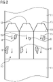
- Fig. 2 shows a top view of the optical unit 10, wherein multiple light sources 13 are provided which are arranged in a defined pattern along a longer edge 19 of the rectangular optical unit 10. Hence, each of the light sources 13 generates radiation 15 coupled into the edge 19 of the optical unit 10.
- the determination unit 14 can determine the intensity of the reflected part 16 of the radiation 15 and therefore, can determine the condition information, in particular the contamination degree. Further, it is possible that the determination unit 14 locally resolves the condition information, e.g. via a detector 17 that is built as a CMOS or CCD-chip, in particular comprising a grid-like shape, for example including a plurality of pixels.
- the condition information can be determined for different positions on the optical unit 10, in particular on the optical surface 9.
- residues 8 adhered to the optical surface 9 are in a critical position through which the energy beam 5 is guided into the process chamber 6, or whether residues 8 are deposited in less important regions of the optical unit 10. Therefore, it is possible to only perform a cleaning process of the optical surface 9, if residues 8 are at least partially adhered to the optical surface 9 in at least one critical position requiring a cleaning of the optical surface 9.
- the map can further be generated as a three-dimensional map, wherein for each layer of the additive manufacturing process, it is possible to locally resolve the condition information.
- the condition information can be stored locally resolved, wherein each process step, such as an irradiation step, can be related to the condition information present during the corresponding irradiation step. Therefore, it is possible to derive whether and to which degree the optical surface 9 was contaminated during the corresponding process step.
- the determination unit 14 may distinguish between the reflected part 16 of radiation 15 reflected from the optical surface 9 that is facing the process chamber 6 and a reflected part 21 of the radiation 15 that is reflected from an optical surface 20 facing the energy source 4, for example facing an irradiation device outside the process chamber 6.
- a contamination of the upper surface of the optical unit 10 for example contaminated via dust or other particles.
- inventive method may be performed on the inventive apparatus 1, preferably using an inventive determination device 12.
Description
- The invention relates to an apparatus for additively manufacturing three-dimensional objects by means of successive layerwise selective consolidation of layers of a build material which can be consolidated by means of an energy source, which apparatus comprises an optical unit with at least one optical surface arranged in a process chamber of the apparatus.
- Apparatuses for additively manufacturing three-dimensional objects comprising optical units with at least one optical surface arranged in a process chamber of the apparatus are generally known from prior art. Typically, such apparatuses comprise a process chamber in which additive manufacturing processes are performed, e.g. in which a (powdery) build material is selectively consolidated to successively build the three-dimensional object.
- Further, it is known from prior art that various optical units, such as windows of the powder chamber or lenses or the like can be used in the additive manufacturing process. Optical surfaces of these optical units, e.g. the surfaces of a lens or a window of the process chamber, e.g. a window through which an energy beam can be guided into the process chamber or a window through which an operator or a determination device may monitor the manufacturing process. Such optical surfaces are exposed to the environment inside the process chamber, i.e. the optical surface that is arranged in the process chamber, e.g. delimiting the process chamber in case of a window, is in direct contact with the environment in the process chamber. During the additive manufacturing process residues are generated, such as soot, smoke or smolder or non-consolidated build material particles, which residues may adhere to the optical surface of the at least one optical unit. Thus, it is possible that the optical surface is successively contaminated thereby, negatively influencing the transmission behavior of the optical surface. For example, an energy beam is at least partially absorbed or scattered/reflected at residues adhered to the optical surface of a window through which the energy beam is coupled/guided into the process chamber.
- Therefore, it is necessary that the respective optical unit is cleaned or exchanged regularly. Typically, a cleaning or an exchange of the optical unit is performed in defined time intervals during an additive manufacturing process or between additive manufacturing processes. However, a cleaning or an exchange of the optical unit may become necessary before the defined time interval or before the additive manufacturing process is over, respectively. Further, if the defined time interval is chosen too short, an exchange or cleaning process is performed too often, wherein the additive manufacturing process is unnecessarily interrupted.
-
US 2016/236279 A1 discloses a laser solidification apparatus for building objects by layerwise solidification of powder material. -
KR 100 709 036 B1 - It is an object of the present invention to provide an improved apparatus for additively manufacturing three-dimensional objects, wherein in particular negative influences of at least one contaminated optical unit on the additive manufacturing process can be reduced or avoided and cleaning or exchange processes of an optical unit can be performed more efficiently.
- The object is inventively achieved by an apparatus according to
claim 1. and a method according toclaim 13. - Advantageous embodiments of the invention are subject to the dependent claims.
- The apparatus described herein is an apparatus for additively manufacturing three-dimensional objects, e.g. technical components, by means of successive selective layerwise consolidation of layers of a powdered build material ("build material") which can be consolidated by means of an energy source, e.g. an energy beam, in particular a laser beam. A respective build material can be a metal, ceramic or polymer powder. A respective energy beam can be a laser beam. A respective apparatus can be an apparatus in which an application of build material and a consolidation of build material is performed separately, such as a selective laser sintering apparatus or a selective laser melting apparatus, for instance. Alternatively, the successive layerwise selective consolidation of build material may be performed via at least one binding material. The binding material may be applied with a corresponding application unit and, for example, irradiated with a suitable energy source, e.g. a UV light source.
- The apparatus may comprise a number of functional units which are used during its operation. Exemplary functional units are a process chamber, an irradiation device which is adapted to selectively irradiate a build material layer disposed in the process chamber with at least one energy beam, and a stream generating device which is adapted to generate a gaseous fluid stream at least partly streaming through the process chamber with given streaming properties, e.g. a given streaming profile, streaming velocity, etc. The gaseous fluid stream is capable of being charged with non-consolidated particulate build material, particularly smoke or smoke residues generated during operation of the apparatus, while streaming through the process chamber. The gaseous fluid stream is typically inert, i.e. typically a stream of an inert gas, e.g. argon, nitrogen, carbon dioxide, etc.
- The invention is based on the idea that the apparatus comprises at least one determination device with at least one light source and at least one determination unit adapted to determine at least one irradiation parameter of radiation emitted by the light source and reflected at the optical surface of the optical unit, wherein the determination device is adapted to determine at least one condition information of the optical unit based on the determined radiation parameter.
- Thus, the determination device can be used to emit radiation via the light source, which is coupled into the optical unit Residues adhered to the optical surface of the optical unit scatter or reflect the radiation, respectively, wherein the determination unit can determine the reflected radiation, in particular at least one radiation parameter of the radiation reflected at the optical surface of the optical unit. In other words, dependent on the residues, in particular the amount of residues, that are adhered to or deposited on the optical surface of the optical unit, a defined ratio of the radiation that is emitted via the light source is reflected towards the determination unit. Therefore, it is possible to determine at least one condition information of the optical unit based on the determined radiation parameter.
- The term "reflected" may refer to any arbitrary way in which a part of the radiation that is generated via the light source is propagating towards the detector. Preferably, radiation is uncoupled from the optical unit due to the residues present on the optical surface. Thus, radiation may be reflected, scattered or otherwise guided towards /detectable with the determination unit.
- The condition information may preferably relate to a contamination degree of the optical surface of the optical unit, in particular to a contamination with residues, and/or an operational state of the optical unit, in particular an integrity of the optical unit, e.g. indicate whether the optical unit is damaged. The term "contamination" may relate to an amount of residues that are adhered to the optical surface of the optical unit. For example, the more residues deposited on the optical surface of the optical unit, the more radiation is guided towards the determination unit. Also, the more residues present on the optical surface, the less radiation, e.g. of an energy beam, can pass the optical unit, as a defined part of the radiation is reflected, scattered or absorbed via the residues. Thus, determining the condition information enables a determination or a decision whether the optical surface of the optical unit needs to be exchanged or cleaned or whether the optical surface is not contaminated with residues.
- As described before, the determination unit may be adapted to determine the radiation parameter of radiation emitted from the light source and reflected at at least one particle adhered to the surface of the optical unit. The term "optical unit" refers to a process window through which the energy beam propagates into the process chamber, e.g. that protects at least one optical component, such as a lens or a lens assembly of an irradiation device, a beam guiding unit, such as a scanner or the like from the conditions inside the process chamber.
- According to a preferred embodiment of the inventive apparatus, the determination unit may be adapted to determine an intensity of the reflected radiation. Since the intensity of the radiation that is determined via the determination unit directly relates to the intensity of radiation that is reflected at residues adhered to the optical surface of the optical unit, it is possible to use the determined intensity of the reflected radiation for determining the contamination information, preferably relating to a degree of contamination of the optical surface.
- In other words, it is possible to determine the intensity of the radiation that is reflected at the optical surface and conclude on or derive the amount of residues that are deposited on the optical surface leading to the reflection of radiation with that corresponding intensity. For example, an optical surface of an optical unit that is free of residues does (dependent on how the radiation is incident on / coupled into the optical unit) not reflect any of the radiation emitted from the light source, whereas related with an increasing amount of residues the intensity that is determined via the determination unit increases.
- The light source is adapted to essentially radially couple the emitted radiation into the optical unit with respect to an optical axis of the optical unit. Therefore, The light source is arranged in that the radiation is coupled radially, namely at a rim or an edge, into the optical unit, such as a window or a lens. Thus, the radiation may propagate through the optical unit without any (additional) reflection, if the optical surface of the optical unit is free of residues. The term "radially" may therefore, be understood as towards the center or a central plane of the optical unit. Each particle adhered to the optical surface leads to an uncoupling of radiation out of the optical unit (radiation leaving the optical unit) and therefore, radiation being reflected at the optical surface of the optical unit that can be detected via the determination unit.
- The light source may, inter alia, be built as light emitting diode (LED) or the light source may comprise at least one optical fiber via which light can be guided to the optical unit and coupled into the optical unit, as described before. The light source may be adapted to emit radiation and couple the radiation into the optical unit. The radiation coupled into the optical unit may essentially propagate in parallel to at least one optical surface of the optical unit, wherein the optical unit behaves as a light conductor. In regions in which residues are present on the optical surface, radiation is decoupled from the optical unit and therefore, can be detected via the determination unit. Due to the optical unit conducting the radiation emitted from the light source, a major part of the radiation propagates through the optical unit towards an opposing side of the optical unit with respect to the position of the light source. The radiation angle under which the light source emits the radiation is preferably chosen in that the radiation is incident on the optical surface from within the optical unit, but a direct propagation of the radiation from the light source to the determination unit is avoided.
- The determination unit and/or the light source may be arranged in that the radiation emitted from the light source cannot directly propagate to the detector of the determination unit, e.g. can propagate along a direct line from the light source to the detector. Thus, it can be assured that radiation emitted by the light source and detected by the determination unit results from residues present on the optical unit and not from the light source itself.
- For example, a lens hood or a lens shade can be used with the determination unit that limits the angle of acceptance under which radiation emitted from the light source can be received by the determination unit. It is also possible to use a suitable filtering unit, e.g. dampening a certain part of the radiation emitted by the light source.
- The light source may preferably be adapted to emit radiation of a different wavelength than radiation emitted by the energy source, preferably in the visual spectrum, in particular blue light. Dependent on the energy source that is used to (selectively) irradiate and consolidate the build material, a wavelength of the light source can be chosen. By providing a light source that is adapted to emit radiation of the different wavelength than the radiation used to consolidate the build material, e.g. the wavelength of an energy beam, it is possible to determine the at least one radiation parameter of the reflected radiation and therefore, determine the condition information without any influence caused by the energy source, e.g. the energy beam being reflected at the optical surface. Hence, if an energy beam, such as a laser beam, with a wavelength in the near infrared spectrum is used to consolidate the build material, it is beneficial to use a light source that is adapted to emit blue light.
- Further, the determination device may comprise a filter unit that is adapted to filter radiation deviant from a wavelength of the light source. Alternatively, the detector of the determination unit may only be sensitive to the radiation emitted from the light source. For example, radiation emitted from the energy source may be filtered and therefore, it may be avoided that radiation emitted by the energy source is incident on the determination unit. It is also possible that the detector is not sensitive for the radiation emitted from the energy source.
- According to another embodiment of the inventive apparatus, the light source of the determination device may at least partially be integrated in a frame of the optical unit, preferably in a wall of the process chamber. As described before, the light source emits radiation radially with respect to the optical axis or a central axis/plane of the optical unit, in particular adapted to radially couple the radiation into the optical unit. The light source may further be integrated in a frame of the optical unit, e.g. a frame that at least partially surrounds the optical unit, wherein the light source is protected from the environment inside the process chamber by the integration in the frame of the optical unit. For example, if the optical unit is integrated in a wall of the process chamber itself, such as a process chamber window, the light source may also be integrated into the wall of the process chamber being arranged in that the light source is adapted to radially emit the radiation towards the center of the optical unit.
- The inventive apparatus may further be improved in that the determination device may be adapted to output at least one signal dependent on the determined condition information, in particular with a degree of contamination above a defined threshold value. Hence, the determination device may continuously or in defined time intervals determine the condition information of the at least one optical unit, e.g. the condition information of a window of the process chamber of the apparatus. Dependent on the determined condition information, e.g. relating to the contamination degree of the optical unit, preferably if the contamination degree is above a defined threshold value, it is possible that the determination device outputs a signal, e.g. indicating that an exchange or a cleaning of the optical surface of the optical unit is necessary. The defined threshold may be defined in that, for example, the signal can be output above a certain intensity of the radiation that is reflected at the optical surface and determined via the determination unit.
- The determination device may further be adapted to initiate an exchange or a cleaning of the at least one optical surface of the optical unit dependent on the condition information. Thus, the signal, as described before, can be used to initiate an exchange or a cleaning process of the at least one optical surface of the optical unit. Therefore, the cleaning process or the exchange process can be performed based on the need for cleaning or exchanging the optical unit assuring that the optical unit is cleaned or exchanged whenever the amount of residues deposited on the optical surface requires an exchange or a cleaning of the optical surface to prevent negative influences on the additive manufacturing process.
- Further, the determination device or a separate control unit may be adapted to compare a determined condition information before and after a cleaning process and adapted to determine at least one cleaning process parameter, in particular a cleaning efficiency. As described before, if the condition information, e.g. the contamination degree of the optical surface is above a defined threshold value, it is possible to initiate a cleaning process. Preferably, the determination device continuously determines the condition information, in particular the contamination degree. The condition information can be determined before and after a cleaning process has been performed and both values of the determined condition information can be compared. Thus, the efficiency of the cleaning process, e.g. the amount of residues removed via the cleaning process, can be determined. Hence, it is possible to determine the status of the cleaning device, e.g. indicating whether the cleaning device itself has to be serviced.
- Preferably, the at least one condition information may be related via the determination device to at least one process step of an additive manufacturing process performed on the apparatus. In other words, it is possible to determine the condition information for more than one process step of the additive manufacturing apparatus, e.g. for multiple irradiation process steps in which build material is selectively irradiated. By relating the condition information, e.g. relating to or indicating the degree to which the optical surface is contaminated with residues, it is possible to conclude on the effects the contamination of the optical surface has on the corresponding process step. Thus, it is possible to determine the effect of the residues adhered to the optical surface, e.g. absorbing a part of the energy beam, during the irradiation of build material.
- It is particularly preferred that the determination unit may be adapted to locally resolve the condition information, in particular adapted to resolve a condition information for at least two different surfaces of the optical unit. According to this embodiment, the determination unit may be used to locally resolve the condition information, for example different regions of a detector of the determination unit. A CCD-chip or a CMOS-sensor may be used to locally resolve the condition information. For example, the optical surface may be imaged onto the detector of the determination unit and therefore, the intensity of radiation incident on the individual pixels can be determined. Thus, it is possible to locally resolve the condition information and therefore, determine which parts or regions of the optical surface are contaminated with residues leading to a corresponding contamination degree.
- It is also possible to resolve the condition information for at least two different surfaces of the optical unit, for example an upper surface and a lower surface of a window in the process chamber, i.e. an optical surface of the window in the process chamber facing inside the process chamber and the opposing optical surface that faces the beam guiding unit, for instance. Preferably, it is possible that based on the locally resolved condition information, a (virtual) map can be generated, preferably a two-dimensional or a three-dimensional map, indicating the locally resolved condition information for manufacturing of at least one layer of the object in the additive manufacturing process. Hence, the map, in particular the two-dimensional map can be used to indicate the condition information of the optical surface two-dimensionally, for example a color-coded information of the contamination degree of the optical surface can be output to an operator of the apparatus.
- It is also possible to generate a three-dimensional map wherein a two-dimensional map is stored for each layer (or selected layers) of the three-dimensional object that is additively built during the manufacturing process, wherein each layer of the three-dimensional map can be displayed color-coded to a user, wherein it is possible that the user may conclude from the three-dimensional map on the condition information of the optical surface during the additive manufacturing process of each layer of the object.
- According to another preferred embodiment of the inventive apparatus, the determination device may comprise at least two light sources arranged in a predefined pattern along the at least one edge of the optical unit, preferably equidistantly along the longest edge and/or circumferentially arranged. Hence, the determination device may comprise more than one light source, for example a plurality of light sources that can be arranged at least partially around the optical unit, in particular in that the light sources can emit radiation that can be coupled into the optical unit, e.g. arranged circumferentially or along the longest edge of the optical unit. For example, if the optical unit is built as process window in the process chamber of the apparatus, light sources may be arranged in parallel along the longest edge of the rectangular process window. Of course, it is also possible to otherwise arrange the plurality of light sources, e.g. at least partially circumferentially around an annular optical unit or the like. By providing more than one light source it is possible to more uniformly distribute the radiation through the optical unit and therefore, improve the detection quality of radiation reflected at the optical surface.
- As described before, the optical unit is built as or may comprise a window of the process chamber, in particular a window separating an irradiation device from the process chamber. Hence, it is possible that the process chamber comprises one or more windows, for example windows that separate an irradiation device from the process chamber. Thus, the window may be used to protect the irradiation device from the conditions inside the process chamber, in particular heat and residues generated in the additive manufacturing process. As these residues successively contaminate the window by adhering to the window, the intensity of an energy beam that is guided through the window is influenced. In particular, an increasing amount of energy is absorbed by residues adhered to the window. Thus, by continuously determining the condition information of the window, in particular the contamination degree of the window, it is possible to determine when an exchange or a cleaning process of the window is necessary.
- Besides, the invention relates a determination device for an apparatus for additively manufacturing three-dimensional objects by means of successive layerwise selective irradiation and consolidation of layers of a build material which can be consolidated by means of an energy source, which apparatus comprises an optical unit with at least one optical surface arranged in a process chamber of the apparatus, wherein the determination device comprises at least one light source and at least one determination unit adapted to determine at least one radiation parameter of radiation emitted from the light source and reflected at the surface of the optical unit, wherein the determination device is adapted to determine at least one condition information of the optical unit based on the determined radiation parameter.
- Further, the invention relates to a method for determining at least one condition information of an optical unit of an apparatus for additively manufacturing three-dimensional objects by means of successive layerwise selective irradiation and consolidation of layers of a build material which can be consolidated by means of an energy source, which apparatus comprises an optical unit with at least one optical surface arranged in a process chamber of the apparatus, wherein at least one radiation parameter of radiation emitted from a light source of a determination device is determined which radiation is reflected from the surface of the optical unit and at least one condition information of the optical unit is determined based on the determined radiation parameter.
- Of course, all details, features and advantages described with respect to the inventive apparatus are fully transferable to the inventive determination device and the inventive method.
- Exemplary embodiments of the invention are described with reference to the Fig. The Fig. are schematic diagrams, wherein
- Fig. 1
- shows a part of an inventive apparatus in side view; and
- Fig. 2
- shows the part of the inventive apparatus of
Fig. 1 in top view. -
Fig. 1 shows anapparatus 1 for additively manufacturing three-dimensional objects 2 by means of successive layerwise selective consolidation of layers of a build material 3 which can be consolidated by means of anenergy source 4, e.g. a laser source adapted to generate anenergy beam 5 such as a laser beam. Theenergy beam 5 is guided into aprocess chamber 6, i.e. a chamber in which the additive manufacturing process for additively manufacturing the three-dimensional object 2 is performed. - As can be derived from
Fig. 1 , theenergy beam 5 is selectively guided across abuild plane 7 i.e. the plane in which build material 3 is arranged to be selectively irradiated and consolidated via theenergy beam 5. In the irradiation processesresidues 8 are generated, such as soot, smoke and smolder or non-consolidated build material particles that are stirred up, for instance. Theresidues 8 can adhere to surfaces inside theprocess chamber 6, for example an optical surface 9 of anoptical unit 10. In this exemplary embodiment, theoptical unit 10 is built as window in awall 11 of theprocess chamber 6. In other words, theenergy beam 5 passes theoptical unit 10 on the beam path along which theenergy beam 5 is guided to thebuild plane 7. - As the
residues 8 can adhere to the optical surface 9 or are deposited on the optical surface 9, the transmission of theenergy beam 5 through theoptical unit 10 can be negatively influenced by theresidues 8. In particular, it is possible that a certain part of theenergy beam 5 is absorbed or scattered or reflected via theresidues 8 adhered to the optical surface 9. Therefore, an exchange, preferably a cleaning process of the optical surface 9 of theoptical unit 10 can become necessary, if a contamination degree indicating that the amount of residues deposited on the optical surface 9 exceeds a defined threshold value. For determining a condition information of theoptical unit 10, for example the contamination degree, theapparatus 1 comprises adetermination device 12 that comprises alight source 13 and adetermination unit 14. Thelight source 13 is adapted to coupleradiation 15 into theoptical unit 10, in particular couple theradiation 15 radially into theoptical unit 10, e.g. towards an optical axis or a central plane of theoptical unit 10. - In this exemplary embodiment, the
optical unit 10 is a rectangular window, wherein thelight source 13 is arranged in thewall 11 of theprocess chamber 6 and adapted to couple theradiation 15 into theoptical unit 10 towards a central plane of theoptical unit 10. Hence, theradiation 15, for example a light beam, propagates through theoptical unit 10, whereinresidues 8 adhered to the optical surface 9cause radiation 15 or at least a part of theradiation 15 to be decoupled from theoptical unit 10 and leave theoptical unit 10, e.g. causing a beam reflected towards thedetermination unit 14. Therefore, areflected part 16 of theradiation 15 is incident on adetector 17 of thedetermination unit 14. - In other words, if no
residues 8 are adhered to the optical surface 9, theradiation 15 can be coupled into theoptical unit 10 without areflected part 16 being reflected and decoupled from theoptical unit 10 viaresidues 8. Thus, thedetermination unit 14 would not detect radiation and therefore, a "dark field" would be captured via thedetermination unit 14. Dependent on the degree of contamination, i.e. the amount ofresidues 8 adhered to the optical surface 9, an increasing part of theradiation 15 is reflected to thedetector 17 of thedetermination unit 14. Thus, the condition information that can be generated via thedetermination device 12 is directly related to the amount ofresidues 8 deposited on or adhered to the optical surface 9. Therefore, the condition information may, inter alia, comprise a contamination degree indicating the degree to which the optical surface 9 is contaminated withresidues 8. It is further possible to determine other conditions of the optical surface 9 such as damages, in particular cracks, in the optical surface 9 leading to a decoupling ofradiation 15, in particular a reflectedpart 16 leaving theoptical unit 10 towards thedetermination unit 14. - Hence, the
determination unit 14 is adapted to determine an intensity of the reflectedpart 16 of theradiation 15, wherein dependent on the intensity that has been determined via thedetermination unit 14, the amount ofresidues 8 adhered to the optical surface 9 can be determined. Dependent on the amount ofresidues 8 adhered to the optical surface 9, thedetermination device 12 is adapted to output at least one signal, in particular a signal can be output to acontrol unit 18. Thecontrol unit 18 may therefore, initiate an exchange or a cleaning process of the at least one optical surface 9 of theoptical unit 10. In other words, if the condition information that is generated via thedetermination unit 14, e.g. based on the intensity of the reflectedpart 16 of theradiation 15 exceeds a defined threshold value, a cleaning process of the optical surface 9 of theoptical unit 10 can be deemed necessary and can be initiated. - Preferably, the condition information is determined continuously or in defined time intervals, wherein it is particularly possible that the condition information can be determined in advance to a cleaning process and after a cleaning process for determining the efficiency of the cleaning process. In other words, it is possible to determine the amount of
residues 8 still adhered to the optical surface 9 after a cleaning process has been performed. -
Fig. 2 shows a top view of theoptical unit 10, wherein multiplelight sources 13 are provided which are arranged in a defined pattern along alonger edge 19 of the rectangularoptical unit 10. Hence, each of thelight sources 13 generatesradiation 15 coupled into theedge 19 of theoptical unit 10. Dependent on theresidues 8 adhered to the optical surface 9, thedetermination unit 14 can determine the intensity of the reflectedpart 16 of theradiation 15 and therefore, can determine the condition information, in particular the contamination degree. Further, it is possible that thedetermination unit 14 locally resolves the condition information, e.g. via adetector 17 that is built as a CMOS or CCD-chip, in particular comprising a grid-like shape, for example including a plurality of pixels. - Thus, it is possible to determine different intensity values of reflected
parts 16 of theradiation 15 locally resolved over theoptical unit 10. Hence, the condition information can be determined for different positions on theoptical unit 10, in particular on the optical surface 9. Hence, it is possible to derive, whetherresidues 8 adhered to the optical surface 9 are in a critical position through which theenergy beam 5 is guided into theprocess chamber 6, or whetherresidues 8 are deposited in less important regions of theoptical unit 10. Therefore, it is possible to only perform a cleaning process of the optical surface 9, ifresidues 8 are at least partially adhered to the optical surface 9 in at least one critical position requiring a cleaning of the optical surface 9. - It is further possible to generate a map of the optical surface 9, indicating the condition information locally resolved. The map can further be generated as a three-dimensional map, wherein for each layer of the additive manufacturing process, it is possible to locally resolve the condition information. Thus, at least one process step, in particular every irradiation step in which build material 3 is irradiated to successively build the three-
dimensional object 2, the condition information can be stored locally resolved, wherein each process step, such as an irradiation step, can be related to the condition information present during the corresponding irradiation step. Therefore, it is possible to derive whether and to which degree the optical surface 9 was contaminated during the corresponding process step. - Additionally, the
determination unit 14 may distinguish between thereflected part 16 ofradiation 15 reflected from the optical surface 9 that is facing theprocess chamber 6 and areflected part 21 of theradiation 15 that is reflected from anoptical surface 20 facing theenergy source 4, for example facing an irradiation device outside theprocess chamber 6. Thus, it is possible to further determine a contamination of the upper surface of theoptical unit 10, for example contaminated via dust or other particles. - Self-evidently, the inventive method may be performed on the
inventive apparatus 1, preferably using aninventive determination device 12.
Claims (13)
- Apparatus (1) for additively manufacturing three-dimensional objects (2) by means of successive layerwise selective consolidation of layers of a build material (3) which can be consolidated by means of an energy source (4), which apparatus (1) comprises an optical unit (10) built as or comprising a window of a process chamber (6) of the apparatus (1), wherein the optical unit (10) comprises at least one optical surface (9) arranged in the process chamber (6) of the apparatus (1), the apparatus (1) comprising at least one determination device (12) with at least one light source (13) and at least one determination unit (14) adapted to determine at least one radiation parameter of radiation (15) emitted from the light source (13) and reflected at the optical surface (9) of the optical unit (10), wherein the determination device (12) is adapted to determine at least one condition information of the optical unit (10) based on the determined radiation parameter, wherein the light source (13) is adapted to essentially radially couple the radiation (15) into the optical unit (10) with respect to an optical axis of the optical unit (10), wherein the light source (13) is arranged in that the radiation is coupled at a rim or an edge into the optical unit (10).
- Apparatus according to claim 1, characterized in that the at least one radiation parameter of radiation (15) is an intensity of the reflected radiation.
- Apparatus according to one of the preceding claims, characterized in that the light source (13) is adapted to emit radiation (15) of a different wavelength than radiation emitted by the energy source (4), preferably in the visual spectrum, in particular blue light.
- Apparatus according to one of the preceding claims, characterized in that the light source (13) of the determination device (12) is at least partially integrated in a frame of the optical unit (10), preferably in a wall (11) of the process chamber (6).
- Apparatus according to one of the preceding claims, characterized in that the determination device (12) is adapted to output at least one signal dependent on the determined condition information, in particular with a degree of contamination above a defined threshold.
- Apparatus according to one of the preceding claims, characterized in that the determination device (12) is adapted to initiate an exchange or a cleaning of the at least one optical surface (9) of the optical unit (10) dependent on the condition information.
- Apparatus according to one of the preceding claims, characterized in that the determination device (12) or a separate control unit (18) is adapted to compare a determined condition information before and after a cleaning process and adapted to determine at least one cleaning process parameter, in particular a cleaning efficiency.
- Apparatus according to one of the preceding claims, characterized in that the determination device (12) or a separate control unit (18) is adapted to relate the at least one condition information to at least one process step of an additive manufacturing process performed on the apparatus (1).
- Apparatus according to one of the preceding claims, characterized in that the determination unit (14) is adapted to locally resolve the condition information, in particular adapted to resolve a condition information for at least two different optical surfaces (9, 20) of the optical unit (10).
- Apparatus according to claim 9, characterized in that the determination unit (14) is adapted to generate a map, preferably a two dimensional or three-dimensional map, indicating the locally resolved condition information for manufacturing of at least one layer of the object (2) in an additive manufacturing process.
- Apparatus according to one of the preceding claims, characterized in that the determination device (12) comprises at least two light sources (13) arranged in a predefined pattern along at least one edge of the optical unit (10), preferably equidistantly along the longest edge (19) and/or circumferentially.
- Apparatus according to one of the preceding claims, characterized in that the optical unit (10) is built as or comprises a window separating an irradiation device from the process chamber (6).
- Method for determining at least one condition information of an optical unit (10) of an apparatus (1) for additively manufacturing three-dimensional objects (2) by means of successive layerwise selective consolidation of layers of a build material (3) which can be consolidated by means of an energy source (4), which apparatus (1) comprises an optical unit (10) built as or comprising a window of a process chamber (6) of the apparatus (1), wherein the optical unit (10) comprises at least one optical surface (9) arranged in a process chamber (6) of the apparatus (1), the method comprising the steps: determining at least one radiation parameter of radiation (15) emitted from a light source (13) of a determination device (12) which radiation is reflected from the optical surface (9) of the optical unit (10) and determining at least one condition information of the optical unit (10) based on the determined radiation parameter, wherein the radiation (15) of the light source (13) is essentially coupled radially into the optical unit (10) with respect to an optical axis of the optical unit (10), wherein the light source (13) is arranged in that the radiation is coupled at a rim or an edge into the optical unit (10).
Priority Applications (2)
| Application Number | Priority Date | Filing Date | Title |
|---|---|---|---|
| EP18200248.5A EP3636415B1 (en) | 2018-10-12 | 2018-10-12 | Apparatus for additively manufacturing three-dimensional objects |
| US16/294,063 US11534971B2 (en) | 2018-10-12 | 2019-03-06 | Apparatus for additively manufacturing three-dimensional objects |
Applications Claiming Priority (1)
| Application Number | Priority Date | Filing Date | Title |
|---|---|---|---|
| EP18200248.5A EP3636415B1 (en) | 2018-10-12 | 2018-10-12 | Apparatus for additively manufacturing three-dimensional objects |
Publications (2)
| Publication Number | Publication Date |
|---|---|
| EP3636415A1 EP3636415A1 (en) | 2020-04-15 |
| EP3636415B1 true EP3636415B1 (en) | 2023-01-04 |
Family
ID=63857724
Family Applications (1)
| Application Number | Title | Priority Date | Filing Date |
|---|---|---|---|
| EP18200248.5A Active EP3636415B1 (en) | 2018-10-12 | 2018-10-12 | Apparatus for additively manufacturing three-dimensional objects |
Country Status (2)
| Country | Link |
|---|---|
| US (1) | US11534971B2 (en) |
| EP (1) | EP3636415B1 (en) |
Families Citing this family (8)
| Publication number | Priority date | Publication date | Assignee | Title |
|---|---|---|---|---|
| DE102014016679A1 (en) | 2014-11-12 | 2016-05-12 | Cl Schutzrechtsverwaltungs Gmbh | Method and device for exposure control of a selective laser sintering or laser melting device |
| JP6907002B2 (en) * | 2017-04-06 | 2021-07-21 | 株式会社小糸製作所 | Three-dimensional surface display device and vehicle display device |
| EP3636415B1 (en) | 2018-10-12 | 2023-01-04 | Concept Laser GmbH | Apparatus for additively manufacturing three-dimensional objects |
| FR3111698B1 (en) * | 2020-06-17 | 2022-12-30 | Safran | Defect detection system in the optical path of an additive manufacturing device |
| US20220111599A1 (en) * | 2020-10-14 | 2022-04-14 | General Electric Company | Systems and methods for handling optical anomalies on optical elements of an additive manufacturing machine |
| US11752558B2 (en) * | 2021-04-16 | 2023-09-12 | General Electric Company | Detecting optical anomalies on optical elements used in an additive manufacturing machine |
| EP4257960A1 (en) * | 2022-04-06 | 2023-10-11 | TRUMPF Additive Manufacturing Italia S.r.l. | Method for monitoring at least one surface of an optical element in an additive manufacturing apparatus and apparatus for additive manufacturing of an object |
| GB202207531D0 (en) | 2022-05-23 | 2022-07-06 | Renishaw Plc | Additive manufacturing apparatus and method |
Family Cites Families (9)
| Publication number | Priority date | Publication date | Assignee | Title |
|---|---|---|---|---|
| US7538310B2 (en) * | 2005-03-31 | 2009-05-26 | Sanyo Electric Co., Ltd. | Laser beam irradiation device with error position detection |
| KR100709036B1 (en) * | 2005-11-18 | 2007-04-18 | 코닉시스템 주식회사 | Laser annealing apparatus having detector for detecting contamination of chamber window |
| GB201316815D0 (en) * | 2013-09-23 | 2013-11-06 | Renishaw Plc | Additive manufacturing apparatus and method |
| DE102014209161A1 (en) * | 2014-05-14 | 2015-11-19 | Eos Gmbh Electro Optical Systems | Control unit, apparatus and method for producing a three-dimensional object |
| EP3229996A4 (en) | 2014-12-12 | 2018-09-05 | Velo3d Inc. | Feedback control systems for three-dimensional printing |
| KR101962053B1 (en) * | 2014-12-26 | 2019-03-25 | 파나소닉 아이피 매니지먼트 가부시키가이샤 | Method for manufacturing three-dimensional molding |
| US20180186082A1 (en) | 2017-01-05 | 2018-07-05 | Velo3D, Inc. | Optics in three-dimensional printing |
| EP3636415B1 (en) | 2018-10-12 | 2023-01-04 | Concept Laser GmbH | Apparatus for additively manufacturing three-dimensional objects |
| US20220111599A1 (en) | 2020-10-14 | 2022-04-14 | General Electric Company | Systems and methods for handling optical anomalies on optical elements of an additive manufacturing machine |
-
2018
- 2018-10-12 EP EP18200248.5A patent/EP3636415B1/en active Active
-
2019
- 2019-03-06 US US16/294,063 patent/US11534971B2/en active Active
Also Published As
| Publication number | Publication date |
|---|---|
| EP3636415A1 (en) | 2020-04-15 |
| US11534971B2 (en) | 2022-12-27 |
| US20200114580A1 (en) | 2020-04-16 |
Similar Documents
| Publication | Publication Date | Title |
|---|---|---|
| EP3636415B1 (en) | Apparatus for additively manufacturing three-dimensional objects | |
| EP0956498B1 (en) | Method and apparatus for checking the condition of a protective glass in connection with laser machining | |
| JP2012187591A (en) | Laser processing head | |
| JP6815689B2 (en) | Laser processing machine | |
| US20230219165A1 (en) | Device for process monitoring in a deposition welding method | |
| JP2009039779A (en) | Method for evaluating quality of laser welding, and apparatus therefor | |
| JP6134805B2 (en) | Optical processing head and three-dimensional modeling apparatus | |
| JP7179278B2 (en) | Device for detecting dirt on protective glass and method for detecting dirt on protective glass | |
| CN109421275B (en) | Apparatus for manufacturing three-dimensional objects | |
| US11119051B2 (en) | Particle detection for substrate processing | |
| JP5414645B2 (en) | Laser processing equipment | |
| JP6757018B2 (en) | Protective glass stain detection device, laser processing machine equipped with it, and protective glass stain detection method | |
| JP6982450B2 (en) | Protective glass stain detection system and method | |
| JP2020179405A (en) | Detection device and detection method for fume contamination on protective glass | |
| EP3572213B1 (en) | Apparatus for additively manufacturing three-dimensional objects and method of operating an apparatus for additive manufacturing | |
| EP3560633B1 (en) | Apparatus for additively manufacturing three-dimensional objects and method for determining at least one parameter of an energy beam | |
| KR102530974B1 (en) | A device for measuring real-time flow and concentration of abnormal fumes generated during the powder bed fusion process, and a method for measuring real-time flow and concentration of abnormal fumes using the same | |
| JP2007024638A (en) | Inspection system and method of laser torch | |
| EP4257960A1 (en) | Method for monitoring at least one surface of an optical element in an additive manufacturing apparatus and apparatus for additive manufacturing of an object | |
| JP7296769B2 (en) | Spatter detection device, laser processing device, and method for detecting spatter | |
| JP2020157342A (en) | Spatter detection device and laser processing device | |
| Valsecchi et al. | Monitoring of the protective glass during laser cladding with active fiber laser | |
| CZ251499A3 (en) | Process and apparatus for checking state of protective glass in connection with laser cutting | |
| KR20040098259A (en) | A pollution level detecting device of protecting glass device in optic head for laser system |
Legal Events
| Date | Code | Title | Description |
|---|---|---|---|
| PUAI | Public reference made under article 153(3) epc to a published international application that has entered the european phase |
Free format text: ORIGINAL CODE: 0009012 |
|
| STAA | Information on the status of an ep patent application or granted ep patent |
Free format text: STATUS: THE APPLICATION HAS BEEN PUBLISHED |
|
| AK | Designated contracting states |
Kind code of ref document: A1 Designated state(s): AL AT BE BG CH CY CZ DE DK EE ES FI FR GB GR HR HU IE IS IT LI LT LU LV MC MK MT NL NO PL PT RO RS SE SI SK SM TR |
|
| AX | Request for extension of the european patent |
Extension state: BA ME |
|
| STAA | Information on the status of an ep patent application or granted ep patent |
Free format text: STATUS: REQUEST FOR EXAMINATION WAS MADE |
|
| 17P | Request for examination filed |
Effective date: 20201014 |
|
| RBV | Designated contracting states (corrected) |
Designated state(s): AL AT BE BG CH CY CZ DE DK EE ES FI FR GB GR HR HU IE IS IT LI LT LU LV MC MK MT NL NO PL PT RO RS SE SI SK SM TR |
|
| STAA | Information on the status of an ep patent application or granted ep patent |
Free format text: STATUS: EXAMINATION IS IN PROGRESS |
|
| 17Q | First examination report despatched |
Effective date: 20220201 |
|
| RIC1 | Information provided on ipc code assigned before grant |
Ipc: B29C 64/364 20170101ALN20220715BHEP Ipc: B29C 64/35 20170101ALN20220715BHEP Ipc: B33Y 50/00 20150101ALI20220715BHEP Ipc: B33Y 30/00 20150101ALI20220715BHEP Ipc: B33Y 10/00 20150101ALI20220715BHEP Ipc: B29C 64/153 20170101ALI20220715BHEP Ipc: B29C 64/386 20170101ALI20220715BHEP Ipc: B29C 64/20 20170101AFI20220715BHEP |
|
| REG | Reference to a national code |
Ref country code: DE Ref legal event code: R079 Ref document number: 602018044948 Country of ref document: DE Free format text: PREVIOUS MAIN CLASS: B29C0064153000 Ipc: B29C0064200000 |
|
| GRAP | Despatch of communication of intention to grant a patent |
Free format text: ORIGINAL CODE: EPIDOSNIGR1 |
|
| STAA | Information on the status of an ep patent application or granted ep patent |
Free format text: STATUS: GRANT OF PATENT IS INTENDED |
|
| RIC1 | Information provided on ipc code assigned before grant |
Ipc: B29C 64/364 20170101ALN20220905BHEP Ipc: B29C 64/35 20170101ALN20220905BHEP Ipc: B33Y 50/00 20150101ALI20220905BHEP Ipc: B33Y 30/00 20150101ALI20220905BHEP Ipc: B33Y 10/00 20150101ALI20220905BHEP Ipc: B29C 64/153 20170101ALI20220905BHEP Ipc: B29C 64/386 20170101ALI20220905BHEP Ipc: B29C 64/20 20170101AFI20220905BHEP |
|
| RIC1 | Information provided on ipc code assigned before grant |
Ipc: B29C 64/364 20170101ALN20220909BHEP Ipc: B29C 64/35 20170101ALN20220909BHEP Ipc: B33Y 50/00 20150101ALI20220909BHEP Ipc: B33Y 30/00 20150101ALI20220909BHEP Ipc: B33Y 10/00 20150101ALI20220909BHEP Ipc: B29C 64/153 20170101ALI20220909BHEP Ipc: B29C 64/386 20170101ALI20220909BHEP Ipc: B29C 64/20 20170101AFI20220909BHEP |
|
| INTG | Intention to grant announced |
Effective date: 20220928 |
|
| GRAS | Grant fee paid |
Free format text: ORIGINAL CODE: EPIDOSNIGR3 |
|
| GRAA | (expected) grant |
Free format text: ORIGINAL CODE: 0009210 |
|
| STAA | Information on the status of an ep patent application or granted ep patent |
Free format text: STATUS: THE PATENT HAS BEEN GRANTED |
|
| AK | Designated contracting states |
Kind code of ref document: B1 Designated state(s): AL AT BE BG CH CY CZ DE DK EE ES FI FR GB GR HR HU IE IS IT LI LT LU LV MC MK MT NL NO PL PT RO RS SE SI SK SM TR |
|
| REG | Reference to a national code |
Ref country code: GB Ref legal event code: FG4D |
|
| REG | Reference to a national code |
Ref country code: DE Ref legal event code: R096 Ref document number: 602018044948 Country of ref document: DE |
|
| REG | Reference to a national code |
Ref country code: CH Ref legal event code: EP |
|
| REG | Reference to a national code |
Ref country code: AT Ref legal event code: REF Ref document number: 1541631 Country of ref document: AT Kind code of ref document: T Effective date: 20230115 |
|
| REG | Reference to a national code |
Ref country code: IE Ref legal event code: FG4D |
|
| REG | Reference to a national code |
Ref country code: LT Ref legal event code: MG9D |
|
| REG | Reference to a national code |
Ref country code: NL Ref legal event code: MP Effective date: 20230104 |
|
| REG | Reference to a national code |
Ref country code: AT Ref legal event code: MK05 Ref document number: 1541631 Country of ref document: AT Kind code of ref document: T Effective date: 20230104 |
|
| P01 | Opt-out of the competence of the unified patent court (upc) registered |
Effective date: 20230515 |
|
| PG25 | Lapsed in a contracting state [announced via postgrant information from national office to epo] |
Ref country code: NL Free format text: LAPSE BECAUSE OF FAILURE TO SUBMIT A TRANSLATION OF THE DESCRIPTION OR TO PAY THE FEE WITHIN THE PRESCRIBED TIME-LIMIT Effective date: 20230104 |
|
| PG25 | Lapsed in a contracting state [announced via postgrant information from national office to epo] |
Ref country code: RS Free format text: LAPSE BECAUSE OF FAILURE TO SUBMIT A TRANSLATION OF THE DESCRIPTION OR TO PAY THE FEE WITHIN THE PRESCRIBED TIME-LIMIT Effective date: 20230104 Ref country code: PT Free format text: LAPSE BECAUSE OF FAILURE TO SUBMIT A TRANSLATION OF THE DESCRIPTION OR TO PAY THE FEE WITHIN THE PRESCRIBED TIME-LIMIT Effective date: 20230504 Ref country code: NO Free format text: LAPSE BECAUSE OF FAILURE TO SUBMIT A TRANSLATION OF THE DESCRIPTION OR TO PAY THE FEE WITHIN THE PRESCRIBED TIME-LIMIT Effective date: 20230404 Ref country code: LV Free format text: LAPSE BECAUSE OF FAILURE TO SUBMIT A TRANSLATION OF THE DESCRIPTION OR TO PAY THE FEE WITHIN THE PRESCRIBED TIME-LIMIT Effective date: 20230104 Ref country code: LT Free format text: LAPSE BECAUSE OF FAILURE TO SUBMIT A TRANSLATION OF THE DESCRIPTION OR TO PAY THE FEE WITHIN THE PRESCRIBED TIME-LIMIT Effective date: 20230104 Ref country code: HR Free format text: LAPSE BECAUSE OF FAILURE TO SUBMIT A TRANSLATION OF THE DESCRIPTION OR TO PAY THE FEE WITHIN THE PRESCRIBED TIME-LIMIT Effective date: 20230104 Ref country code: ES Free format text: LAPSE BECAUSE OF FAILURE TO SUBMIT A TRANSLATION OF THE DESCRIPTION OR TO PAY THE FEE WITHIN THE PRESCRIBED TIME-LIMIT Effective date: 20230104 Ref country code: AT Free format text: LAPSE BECAUSE OF FAILURE TO SUBMIT A TRANSLATION OF THE DESCRIPTION OR TO PAY THE FEE WITHIN THE PRESCRIBED TIME-LIMIT Effective date: 20230104 |
|
| PG25 | Lapsed in a contracting state [announced via postgrant information from national office to epo] |
Ref country code: SE Free format text: LAPSE BECAUSE OF FAILURE TO SUBMIT A TRANSLATION OF THE DESCRIPTION OR TO PAY THE FEE WITHIN THE PRESCRIBED TIME-LIMIT Effective date: 20230104 Ref country code: PL Free format text: LAPSE BECAUSE OF FAILURE TO SUBMIT A TRANSLATION OF THE DESCRIPTION OR TO PAY THE FEE WITHIN THE PRESCRIBED TIME-LIMIT Effective date: 20230104 Ref country code: IS Free format text: LAPSE BECAUSE OF FAILURE TO SUBMIT A TRANSLATION OF THE DESCRIPTION OR TO PAY THE FEE WITHIN THE PRESCRIBED TIME-LIMIT Effective date: 20230504 Ref country code: GR Free format text: LAPSE BECAUSE OF FAILURE TO SUBMIT A TRANSLATION OF THE DESCRIPTION OR TO PAY THE FEE WITHIN THE PRESCRIBED TIME-LIMIT Effective date: 20230405 Ref country code: FI Free format text: LAPSE BECAUSE OF FAILURE TO SUBMIT A TRANSLATION OF THE DESCRIPTION OR TO PAY THE FEE WITHIN THE PRESCRIBED TIME-LIMIT Effective date: 20230104 |
|
| REG | Reference to a national code |
Ref country code: DE Ref legal event code: R097 Ref document number: 602018044948 Country of ref document: DE |
|
| PG25 | Lapsed in a contracting state [announced via postgrant information from national office to epo] |
Ref country code: SM Free format text: LAPSE BECAUSE OF FAILURE TO SUBMIT A TRANSLATION OF THE DESCRIPTION OR TO PAY THE FEE WITHIN THE PRESCRIBED TIME-LIMIT Effective date: 20230104 Ref country code: RO Free format text: LAPSE BECAUSE OF FAILURE TO SUBMIT A TRANSLATION OF THE DESCRIPTION OR TO PAY THE FEE WITHIN THE PRESCRIBED TIME-LIMIT Effective date: 20230104 Ref country code: EE Free format text: LAPSE BECAUSE OF FAILURE TO SUBMIT A TRANSLATION OF THE DESCRIPTION OR TO PAY THE FEE WITHIN THE PRESCRIBED TIME-LIMIT Effective date: 20230104 Ref country code: DK Free format text: LAPSE BECAUSE OF FAILURE TO SUBMIT A TRANSLATION OF THE DESCRIPTION OR TO PAY THE FEE WITHIN THE PRESCRIBED TIME-LIMIT Effective date: 20230104 Ref country code: CZ Free format text: LAPSE BECAUSE OF FAILURE TO SUBMIT A TRANSLATION OF THE DESCRIPTION OR TO PAY THE FEE WITHIN THE PRESCRIBED TIME-LIMIT Effective date: 20230104 |
|
| PGFP | Annual fee paid to national office [announced via postgrant information from national office to epo] |
Ref country code: GB Payment date: 20230920 Year of fee payment: 6 |
|
| PLBE | No opposition filed within time limit |
Free format text: ORIGINAL CODE: 0009261 |
|
| STAA | Information on the status of an ep patent application or granted ep patent |
Free format text: STATUS: NO OPPOSITION FILED WITHIN TIME LIMIT |
|
| PG25 | Lapsed in a contracting state [announced via postgrant information from national office to epo] |
Ref country code: SK Free format text: LAPSE BECAUSE OF FAILURE TO SUBMIT A TRANSLATION OF THE DESCRIPTION OR TO PAY THE FEE WITHIN THE PRESCRIBED TIME-LIMIT Effective date: 20230104 |
|
| PGFP | Annual fee paid to national office [announced via postgrant information from national office to epo] |
Ref country code: FR Payment date: 20230920 Year of fee payment: 6 |
|
| 26N | No opposition filed |
Effective date: 20231005 |
|
| PG25 | Lapsed in a contracting state [announced via postgrant information from national office to epo] |
Ref country code: SI Free format text: LAPSE BECAUSE OF FAILURE TO SUBMIT A TRANSLATION OF THE DESCRIPTION OR TO PAY THE FEE WITHIN THE PRESCRIBED TIME-LIMIT Effective date: 20230104 |
|
| PGFP | Annual fee paid to national office [announced via postgrant information from national office to epo] |
Ref country code: DE Payment date: 20230920 Year of fee payment: 6 |