EP3633361A2 - Method of generating elemental map and surface analyzer - Google Patents
Method of generating elemental map and surface analyzer Download PDFInfo
- Publication number
- EP3633361A2 EP3633361A2 EP19201511.3A EP19201511A EP3633361A2 EP 3633361 A2 EP3633361 A2 EP 3633361A2 EP 19201511 A EP19201511 A EP 19201511A EP 3633361 A2 EP3633361 A2 EP 3633361A2
- Authority
- EP
- European Patent Office
- Prior art keywords
- correction
- generating
- specimen
- elemental map
- channel images
- Prior art date
- Legal status (The legal status is an assumption and is not a legal conclusion. Google has not performed a legal analysis and makes no representation as to the accuracy of the status listed.)
- Granted
Links
Images




Classifications
-
- G—PHYSICS
- G06—COMPUTING OR CALCULATING; COUNTING
- G06T—IMAGE DATA PROCESSING OR GENERATION, IN GENERAL
- G06T5/00—Image enhancement or restoration
- G06T5/90—Dynamic range modification of images or parts thereof
- G06T5/92—Dynamic range modification of images or parts thereof based on global image properties
-
- G—PHYSICS
- G01—MEASURING; TESTING
- G01N—INVESTIGATING OR ANALYSING MATERIALS BY DETERMINING THEIR CHEMICAL OR PHYSICAL PROPERTIES
- G01N23/00—Investigating or analysing materials by the use of wave or particle radiation, e.g. X-rays or neutrons, not covered by groups G01N3/00 – G01N17/00, G01N21/00 or G01N22/00
- G01N23/22—Investigating or analysing materials by the use of wave or particle radiation, e.g. X-rays or neutrons, not covered by groups G01N3/00 – G01N17/00, G01N21/00 or G01N22/00 by measuring secondary emission from the material
- G01N23/227—Measuring photoelectric effect, e.g. photoelectron emission microscopy [PEEM]
- G01N23/2273—Measuring photoelectron spectrum, e.g. electron spectroscopy for chemical analysis [ESCA] or X-ray photoelectron spectroscopy [XPS]
-
- G—PHYSICS
- G01—MEASURING; TESTING
- G01N—INVESTIGATING OR ANALYSING MATERIALS BY DETERMINING THEIR CHEMICAL OR PHYSICAL PROPERTIES
- G01N23/00—Investigating or analysing materials by the use of wave or particle radiation, e.g. X-rays or neutrons, not covered by groups G01N3/00 – G01N17/00, G01N21/00 or G01N22/00
- G01N23/22—Investigating or analysing materials by the use of wave or particle radiation, e.g. X-rays or neutrons, not covered by groups G01N3/00 – G01N17/00, G01N21/00 or G01N22/00 by measuring secondary emission from the material
- G01N23/227—Measuring photoelectric effect, e.g. photoelectron emission microscopy [PEEM]
- G01N23/2276—Measuring photoelectric effect, e.g. photoelectron emission microscopy [PEEM] using the Auger effect, e.g. Auger electron spectroscopy [AES]
-
- G—PHYSICS
- G06—COMPUTING OR CALCULATING; COUNTING
- G06T—IMAGE DATA PROCESSING OR GENERATION, IN GENERAL
- G06T5/00—Image enhancement or restoration
- G06T5/50—Image enhancement or restoration using two or more images, e.g. averaging or subtraction
-
- G—PHYSICS
- G06—COMPUTING OR CALCULATING; COUNTING
- G06T—IMAGE DATA PROCESSING OR GENERATION, IN GENERAL
- G06T7/00—Image analysis
- G06T7/40—Analysis of texture
-
- G—PHYSICS
- G01—MEASURING; TESTING
- G01N—INVESTIGATING OR ANALYSING MATERIALS BY DETERMINING THEIR CHEMICAL OR PHYSICAL PROPERTIES
- G01N2223/00—Investigating materials by wave or particle radiation
- G01N2223/40—Imaging
- G01N2223/401—Imaging image processing
-
- G—PHYSICS
- G06—COMPUTING OR CALCULATING; COUNTING
- G06T—IMAGE DATA PROCESSING OR GENERATION, IN GENERAL
- G06T2207/00—Indexing scheme for image analysis or image enhancement
- G06T2207/10—Image acquisition modality
- G06T2207/10056—Microscopic image
- G06T2207/10061—Microscopic image from scanning electron microscope
Definitions
- an elemental map (an Auger map) can be acquired by irradiating each measurement point on a specimen surface with an electron beam to scan the measurement point with the electron beam and detecting Auger electrons emitted from each measurement point.
- an elemental map (an Auger map) indicating a distribution of elements can be acquired.
- the surface analyzer 100 acquires an elemental map by scanning a surface of the specimen S with an electron beam, analyzing Auger electrons emitted from the specimen S with a spectrometer 40, and detecting the analyzed Auger electrons with a detector 50 having a plurality of channels capable of detecting electrons with energies that differ from one another.
- the plurality of channeltrons 52 are arranged so that an energy interval ⁇ E between adjacent channeltrons 52 is the same. Therefore, when energy that can be detected by the ch0 channeltron 52 is denoted by E, energy that can be detected by the ch-1 channeltron 52 is denoted by E - ⁇ E, energy that can be detected by the ch-2 channeltron 52 is denoted by E - 2 ⁇ ⁇ E, and energy that can be detected by the ch-3 channeltron 52 is denoted by E - 3 ⁇ ⁇ E.
- the image processing unit 74 performs a process of generating an elemental map. Details of the process by the image processing unit 74 will be described later in "3. Processes".
- FIG. 5 illustrates correction channel images and an elemental map (an Auger map) obtained by measuring a standard specimen.
- the correction channel images in FIG. 5 are images obtained by PB simultaneous measurement.
- the effect of a positional dependence of the sensitivity of the detector 50 is manifested in brightness of the elemental map regardless of whether PB separate measurement or PB simultaneous measurement is performed.
Landscapes
- Physics & Mathematics (AREA)
- General Physics & Mathematics (AREA)
- Engineering & Computer Science (AREA)
- Biochemistry (AREA)
- Chemical & Material Sciences (AREA)
- Analytical Chemistry (AREA)
- Life Sciences & Earth Sciences (AREA)
- General Health & Medical Sciences (AREA)
- Health & Medical Sciences (AREA)
- Immunology (AREA)
- Pathology (AREA)
- Spectroscopy & Molecular Physics (AREA)
- Theoretical Computer Science (AREA)
- Computer Vision & Pattern Recognition (AREA)
- Analysing Materials By The Use Of Radiation (AREA)
Abstract
Description
- The present invention relates to a method of generating an elemental map and to a surface analyzer.
- As surface analyzers, an Auger electron microscope (AES) and an X-ray photoelectron spectroscope (XPS) are well known (for example, refer to
JP-A-2017-111022 - For example, with an Auger electron microscope, an elemental map (an Auger map) can be acquired by irradiating each measurement point on a specimen surface with an electron beam to scan the measurement point with the electron beam and detecting Auger electrons emitted from each measurement point.
- With an Auger electron microscope, analyzed Auger electrons are detected by a detector having a plurality of channels capable of detecting electrons with different energies in a mutually independent manner. As such a detector, a detector equipped with a plurality of channeltrons is known.
- Sensitivity of the detector described above is dependent on a position of a light source or, in other words, a position of a measurement point that is a generation source of Auger electrons. Therefore, in some cases, when acquiring an elemental map, the sensitivity of the detector changes at each measurement point and creates a variation in brightness on the elemental map. In particular, a positional dependence of the sensitivity of the detector has a significant impact in low-magnification measurement.
- According to a first aspect of the invention, there is provided a method of generating an elemental map in a surface analyzer which acquires an elemental map by scanning a surface of a specimen with a primary beam, separating signals emitted from the specimen with a spectrometer, and detecting the separated signals with a detector having a plurality of channels capable of detecting the signals having energies that differ from one another, the method of generating an elemental map including:
- acquiring a plurality of correction channel images by scanning a surface of a standard specimen having a uniform elemental concentration with the primary beam and generating a correction channel image for each of the channels;
- generating correction information for each pixel of each correction channel image among the plurality of correction channel images based on a brightness value of the pixel;
- acquiring a plurality of analysis channel images by scanning a surface of a specimen to be analyzed with the primary beam and generating an analysis channel image for each of the channels;
- correcting brightness values of pixels constituting an analysis channel image among the plurality of analysis channel images based on the correction information; and
- generating the elemental map of the specimen to be analyzed based on the plurality of analysis channel images having the pixels with corrected brightness values.
- According to a second aspect of the invention, there is provided a surface analyzer including:
- a scanning unit which scans a surface of a specimen with a primary beam;
- a spectrometer which separates signals emitted from the specimen;
- a detector which detects the signals separated by the spectrometer with a plurality of channels capable of detecting the signals having energies that differ from one another; and
- an image processing unit which generates an elemental map,
- the image processing unit performing the processes of:
- acquiring a plurality of analysis channel images obtained by scanning a surface of a specimen to be analyzed with the primary beam ;
- correcting brightness values of pixels constituting an analysis channel image among the plurality of analysis channel images based on correction information which corrects a positional dependence of sensitivity of the detector; and
- generating the elemental map of the specimen to be analyzed based on the plurality of analysis channel images having the pixels with corrected brightness values.
-
-
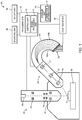
FIG. 1 is a diagram illustrating a configuration of a surface analyzer according to an embodiment of the invention. -
FIG. 2 is a diagram schematically illustrating a detector. -
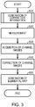
FIG. 3 is a flowchart illustrating an example of a method of generating an elemental map according to an embodiment of the invention. -
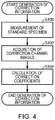
FIG. 4 is a flow chart illustrating an example of a process of generating correction information. -
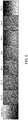
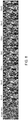
FIG. 5 illustrates correction channel images and an elemental map obtained by measuring a standard specimen. -
FIG. 6 illustrates correction coefficients. -
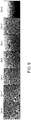
FIG. 7 illustrates analysis channel images and an elemental map obtained by measuring a specimen to be analyzed. -
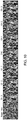
FIG. 8 illustrates analysis channel images after correction and an elemental map after correction. -
FIG. 9 illustrates correction coefficients calculated by using correction channel images having been subjected to a smoothing process. -
FIG. 10 illustrates analysis channel images and an elemental map both corrected by using correction coefficients calculated by using correction channel images having been subjected to a smoothing process. -
FIG. 11 illustrates the elemental map inFIG. 8 and the elemental map inFIG. 10 for comparison. - According to an embodiment of the invention, there is provided a method of generating an elemental map in a surface analyzer which acquires an elemental map by scanning a surface of a specimen with a primary beam, separating signals emitted from the specimen with a spectrometer, and detecting the separated signals with a detector having a plurality of channels capable of detecting the signals having energies that differ from one another, the method of generating an elemental map including:
- acquiring a plurality of correction channel images by scanning a surface of a standard specimen having a uniform elemental concentration with the primary beam and generating a correction channel image for each of the channels;
- generating correction information for each pixel of each correction channel image among the plurality of correction channel images based on a brightness value of the pixel;
- acquiring a plurality of analysis channel images by scanning a surface of a specimen to be analyzed with the primary beam and generating an analysis channel image for each of the channels;
- correcting brightness values of pixels constituting an analysis channel image among the plurality of analysis channel images based on the correction information; and
- generating the elemental map of the specimen to be analyzed based on the plurality of analysis channel images having the pixels with corrected brightness values.
- With such a method of generating an elemental map, since an elemental map is generated by correcting brightness values of pixels constituting an analysis channel image based on the correction information, an elemental map in which variation in brightness attributable to a positional dependence of sensitivity of the detector is reduced can be generated.
- According to an embodiment of the invention, there is provided a surface analyzer including:
- a scanning unit which scans a surface of a specimen with a primary beam;
- a spectrometer which separates signals emitted from the specimen;
- a detector which detects the signals separated by the spectrometer with a plurality of channels capable of detecting the signals having energies that differ from one another; and
- an image processing unit which generates an elemental map,
- the image processing unit performing the processes of:
- acquiring a plurality of analysis channel images obtained by scanning a surface of a specimen to be analyzed with the primary beam;
- correcting brightness values of pixels constituting an analysis channel image among the plurality of analysis channel images based on correction information which corrects a positional dependence of sensitivity of the detector; and
- generating the elemental map of the specimen to be analyzed based on the plurality of analysis channel images having the pixels with corrected brightness values.
- With such a surface analyzer, since an elemental map is generated by correcting brightness values of pixels constituting an analysis channel image based on the correction information, an elemental map in which variation in brightness attributable to a positional dependence of sensitivity of the detector is reduced can be generated.
- Embodiments of the invention are described in detail below with reference to the drawings. Note that the following embodiments do not unduly limit the scope of the invention as stated in the claims. In addition, all of the elements described below are not necessarily essential requirements of the invention.
- First, a surface analyzer according to an embodiment of the invention will be described with reference to the drawings.
FIG. 1 is a diagram illustrating a configuration of asurface analyzer 100 according to an embodiment of the invention. - The
surface analyzer 100 is an apparatus for analyzing a specimen S using Auger electron spectroscopy. Auger electron spectroscopy refers to a method of elemental analysis which is performed by measuring energy of Auger electrons excited by an electron beam or the like and emitted from the specimen S. - With the
surface analyzer 100, an elemental map (an Auger map) indicating a distribution of elements can be acquired. Specifically, thesurface analyzer 100 acquires an elemental map by scanning a surface of the specimen S with an electron beam, analyzing Auger electrons emitted from the specimen S with aspectrometer 40, and detecting the analyzed Auger electrons with adetector 50 having a plurality of channels capable of detecting electrons with energies that differ from one another. - As illustrated in
FIG. 1 , thesurface analyzer 100 includes anelectron source 10, anoptical system 20, aspecimen stage 30, thespectrometer 40, thedetector 50, acounting device 60, aprocessing unit 70, an operatingunit 80, adisplay unit 82, and astorage unit 84. - The
electron source 10 generates an electron beam. Theelectron source 10 is, for example, an electron gun which accelerates electrons emitted from a cathode by an anode and which emits an electron beam. - The
optical system 20 irradiates a specimen S with an electron beam emitted from theelectron source 10. Theoptical system 20 is configured so as to include acondenser lens 22, anobjective lens 24, and adeflector 26 as an example of the scanning unit. - The
condenser lens 22 and theobjective lens 24 focus an electron beam discharged from theelectron source 10. An electron probe can be formed by focusing an electron beam emitted from theelectron source 10 with thecondenser lens 22 and theobjective lens 24. - The
deflector 26 deflects the electron probe focused by thecondenser lens 22 and theobjective lens 24. Thedeflector 26 is used in order to scan an electron beam over a surface of the specimen S. - The
specimen stage 30 holds the specimen S. Thespecimen stage 30 is equipped with a horizontal direction moving mechanism which moves the specimen S in a horizontal direction, a height direction moving mechanism which moves the specimen S in a height direction, and a tilting mechanism which tilts the specimen S. The specimen S can be positioned by thespecimen stage 30. - The
spectrometer 40 analyzes Auger electrons generated by the specimen S when the specimen S is irradiated with an electron beam. Thespectrometer 40 is configured so as to include aninput lens 42 and a hemisphericalelectrostatic analyzer 44. - The
input lens 42 guides incident electrons to the hemisphericalelectrostatic analyzer 44. In addition, theinput lens 42 makes energy resolution variable by decelerating the electrons. In theinput lens 42, although the greater the deceleration of the electrons, the higher the resolution, sensitivity decreases. - The hemispherical
electrostatic analyzer 44 has a hemisphericalinner electrode 44a and a hemisphericalouter electrode 44b. In the hemisphericalelectrostatic analyzer 44, by applying voltage between the hemisphericalinner electrode 44a and the hemisphericalouter electrode 44b, electrons in an energy range in accordance with the applied voltage can be collected. - The
detector 50 detects electrons analyzed by thespectrometer 40. Thedetector 50 has a plurality of channels capable of independently detecting electrons with energies that differ from one another. -
FIG. 2 is a diagram schematically illustrating thedetector 50. Thedetector 50 is configured so as to include a plurality of channeltrons 52. The plurality of channeltrons 52 constitute a plurality of channels capable of independently detecting electrons with energies that differ from one another. - While the
detector 50 has seven channeltrons 52 in the example illustrated inFIG. 2 , the number of channeltrons 52 is not particularly limited. The channeltrons 52 detect electrons and output an amplified signal. - The plurality of channeltrons 52 are arranged side by side in an energy dispersion direction A of electrons on an exit plane of the
spectrometer 40 or, in other words, on an energy dispersion surface. Therefore, the plurality of channeltrons 52 are capable of independently detecting electrons with energies that differ from one another. Accordingly, thedetector 50 is capable of simultaneously detecting electrons with energies that differ from one another. - The plurality of channeltrons 52 are assigned channel numbers. Specifically, ch0 is assigned to the channeltron 52 which detects electrons passing a center between the hemispherical
inner electrode 44a and the hemisphericalouter electrode 44b. In addition, channel ch-1, channel ch-2, and channel ch-3 are respectively assigned to the three channeltrons 52 sequentially arranged toward the side of the hemisphericalinner electrode 44a from the ch0 channeltron 52. Furthermore, channel ch+1, channel ch+2, and channel ch+3 are respectively assigned to the three channeltrons 52 sequentially arranged toward the side of the hemisphericalouter electrode 44b from the ch0 channeltron 52. - The plurality of channeltrons 52 are arranged so that an energy interval ΔE between adjacent channeltrons 52 is the same. Therefore, when energy that can be detected by the ch0 channeltron 52 is denoted by E, energy that can be detected by the ch-1 channeltron 52 is denoted by E - ΔE, energy that can be detected by the ch-2 channeltron 52 is denoted by E - 2 × ΔE, and energy that can be detected by the ch-3 channeltron 52 is denoted by E - 3 × ΔE. In addition, energy that can be detected by the ch+1 channeltron 52 is denoted by E + ΔE, energy that can be detected by the ch+2 channeltron 52 is denoted by E + 2 × ΔE, and energy that can be detected by the ch+3 channeltron 52 is denoted by E + 3 × ΔE.
- The operating
unit 80 performs a process of converting an instruction from a user into a signal and sending the signal to theprocessing unit 70. For example, the operatingunit 80 can be realized by an input device such as a button, a key, a touch panel display, or a microphone. - The
display unit 82 displays an image generated by theprocessing unit 70. Thedisplay unit 82 can be realized by a display such as a liquid crystal display (LCD). - The
storage unit 84 stores programs and data which enable theprocessing unit 70 to perform various calculation processes and control processes. In addition, thestorage unit 84 is also used as a work area of theprocessing unit 70. Thestorage unit 84 can be realized by, for example, a random access memory (RAM), a read only memory (ROM), and a hard disk.Correction information 2 is stored in thestorage unit 84. A description of thecorrection information 2 will be provided later. - The
processing unit 70 performs processes including processes for controlling the respective parts constituting thesurface analyzer 100 and a process of generating an elemental map. Functions of theprocessing unit 70 can be realized by having various processors (a central processing unit (CPU) and the like) execute programs. It should be noted that at least part of the functions of theprocessing unit 70 may be realized by a dedicated circuit such as an ASIC (a gate array or the like). Theprocessing unit 70 includes acontrol unit 72 and animage processing unit 74. - The
control unit 72 controls theoptical system 20 so that, for example, an electron beam is scanned in a desired region on a surface of the specimen S. In addition, thecontrol unit 72 controls theoptical system 20 and thespectrometer 40 in order to perform a measurement (for example, an elemental mapping) of the specimen S. - The
image processing unit 74 performs a process of generating an elemental map. Details of the process by theimage processing unit 74 will be described later in "3. Processes". - The
counting device 60 counts electrons detected by the channeltrons 52. Thecounting device 60 counts detected electrons for each of the plurality of channeltrons 52. Thecounting device 60 receives output signals of the plurality of channeltrons 52 and counts electrons for each energy. Thecounting device 60 sends a count result of electrons for each energy to theprocessing unit 70. A count result is, for example, a count rate. A count rate represents the number of electrons counted within a unit time. - Next, operations of the
surface analyzer 100 will be described. Hereinafter, a case where an elemental mapping is performed in thesurface analyzer 100 will be described. - An electron beam discharged from the
electron source 10 is focused by thecondenser lens 22 and theobjective lens 24 and irradiates the specimen S. At this point, the electron beam is scanned over a surface of the specimen S by using thedeflector 26. Auger electrons, secondary electrons, backscattered electrons, and the like are discharged from a measurement point of the specimen S irradiated by the electron beam. - The Auger electrons and the like discharged from the specimen S are incident into and decelerated by the
input lens 42. The decelerated Auger electrons are analyzed by the hemisphericalelectrostatic analyzer 44 and, as illustrated inFIG. 2 , dispersed in accordance with energy in the energy dispersion direction A on an exit plane of the hemisphericalelectrostatic analyzer 44. - The Auger electrons dispersed in accordance with energy are detected by the plurality of channeltrons 52 arranged side by side in the energy dispersion direction A. The electrons detected by the plurality of channeltrons 52 are counted by the
counting device 60 for each channeltron 52 and a count result thereof is sent to theprocessing unit 70. - In the
processing unit 70, based on the count result for each channeltron 52, a channel image is generated for each channeltron 52. Since thedetector 50 has seven channeltrons 52 in the example illustrated inFIG. 2 , seven channel images are generated. In theprocessing unit 70, an elemental map is generated based on the channel image generated for each channeltron 52 (in the example illustrated inFIG. 2 , seven channel images). A method of generating the elemental map will be described later in "2. Method of generating elemental map". - In this case, as described earlier, not only Auger electrons but secondary electrons, backscattered electrons, and the like are also discharged from the specimen S when irradiated by an electron beam. Since a signal discharged from the specimen S includes Auger electrons as well as other electrons in this manner, a signal (an Auger peak) due to the Auger electrons must be separated from signals (background) of other electrons.
- Methods of separating the background include a method of performing two measurements (hereinafter, also referred to as "PB separate measurement") and a method of performing one measurement (hereinafter, also referred to as "PB simultaneous measurement").
- In PB separate measurement, first, a measurement (a mapping) of an Auger peak corresponding to a desired element is performed to acquire a map (hereinafter, also referred to as a "peak map"). Next, a measurement (a mapping) of the background is performed in a vicinity of the Auger peak corresponding to the desired element to acquire a map (hereinafter, also referred to as a "background map"). The background can be removed from the peak map by subtracting the background map from the peak map. In this manner, an elemental map (an Auger map) is obtained.
- In PB simultaneous measurement, by using a plurality of channeltrons 52, a measurement of an Auger peak and a measurement of a background in the vicinity of the Auger peak are simultaneously performed. Accordingly, in PB simultaneous measurement, a peak map and a background map are obtained by one measurement. Therefore, in PB simultaneous measurement, an elemental map can be obtained in an efficient manner.
- Next, a method of generating an elemental map according to an embodiment of the invention will be described with reference to the drawings.
FIG. 3 is a flowchart illustrating an example of the method of generating an elemental map according to an embodiment of the invention. - First,
correction information 2 for correcting brightness of an elemental map is generated. In this case, sensitivity of thedetector 50 is dependent on a position of a measurement point on the surface of the specimen S. Thecorrection information 2 is information for correcting a positional dependence of the sensitivity of thedetector 50. -
FIG. 4 is a flow chart illustrating an example of a process of generating thecorrection information 2. - As the standard specimen, when the sensitivity of the
detector 50 is not positionally dependent, a specimen is used from which an elemental map with uniform brightness is obtained. Specifically, the standard specimen is a specimen having uniform elemental concentration. In addition, the standard specimen is preferably flat. Examples of such a standard specimen include semiconductor wafers such as a silicon wafer. Performing an elemental mapping of the standard specimen enables an elemental map with uniform brightness to be obtained when the sensitivity of thedetector 50 is not positionally dependent. The measurement of the standard specimen is performed by, for example, PB simultaneous measurement. - By measuring the standard specimen, in the
processing unit 70, a correction channel image is generated for each channeltron 52. Accordingly, the processing unit 70 (the image processing unit 74) can acquire seven correction channel images. -
FIG. 5 illustrates correction channel images and an elemental map (an Auger map) obtained by measuring a standard specimen. The correction channel images inFIG. 5 are images obtained by PB simultaneous measurement. - As illustrated in
FIG. 5 , in thesurface analyzer 100, seven channel images are obtained in correspondence to the seven channeltrons 52. For example, a channel image of ch0 is an image indicating a distribution of intensities (count rates) of electrons obtained by detecting, with the ch0 channeltron 52, electrons discharged from the standard specimen when an electron beam is scanned over a surface of the standard specimen. A brightness value of a pixel constituting a channel image corresponds to an intensity (a count rate) of electrons at a measurement point corresponding to the pixel. The seven channel images are images obtained by detecting electrons with energies that differ from one another. - An elemental map (an Auger map) is generated based on a plurality of correction channel images. For example, a brightness value of a pixel constituting a channel image is represented by Ach (x,y,ch), where x denotes a pixel number in a horizontal direction of the channel image, y denotes a pixel number in a vertical direction of the channel image, and ch denotes a channel number. When generating an elemental map based on the seven channel images in
FIG. 5 , a brightness value Amap (x,y) of an image constituting the elemental map is represented by the following equation.
- As used herein, F denotes a function of calculating an elemental map from a plurality of channel images during PB simultaneous measurement.
- As illustrated in
FIG. 5 , the elemental map (the Auger map) exhibits a variation in brightness. Since the standard specimen is a specimen from which an elemental map with uniform brightness is obtained, the variation in brightness is attributable to thesurface analyzer 100. - In this case, the effect of a positional dependence of the sensitivity of the
detector 50 is manifested in brightness of the elemental map regardless of whether PB separate measurement or PB simultaneous measurement is performed. - In addition, in PB separate measurement, since a measurement of an Auger peak and a measurement of a background can be performed with the same channeltron 52, an individual difference among a plurality of channeltrons 52 does not affect the brightness of the elemental map. On the other hand, in PB simultaneous measurement, since a plurality of channeltrons 52 measure electrons with energies that differ from one another, an individual difference among the plurality of channeltrons 52 affects the brightness of the elemental map.
- In this manner, in PB simultaneous measurement, an effect of the positional dependence of the sensitivity of the
detector 50 and an effect of the individual difference among the plurality of channeltrons 52 are manifested on the elemental map as variations in brightness. - The
correction information 2 is obtained by calculating a correction coefficient at which the variation in brightness of the elemental map inFIG. 5 is eliminated. The correction coefficient is generated for each pixel of a correction channel image based on a brightness value of the pixel in each of the plurality of correction channel images. For example, the correction coefficient is a coefficient in which a value obtained by multiplying the brightness value of a pixel constituting a correction channel image by the coefficient becomes constant. For example, a correction coefficient C (x,y,ch) can be obtained by equation (1) below.
- As used herein, E(n) denotes an average value of all pixels constituting a correction channel image of channel n (n = -3, -2, -1, 0, +1, +2, +3). In this manner, the correction coefficient can be calculated by dividing an average value of brightness values of all pixels constituting a correction channel image by each brightness value of all pixels constituting the correction channel image.
- It should be noted that an average value of brightness values of pixels constituting a center portion of a correction channel image can be used as the average value E(ch). Accordingly, pixels constituting an outer peripheral portion of the correction channel image can be excluded from the calculation. Sensitivity of the channeltrons 52 is low in the outer peripheral portion of a correction channel image. Therefore, excluding the pixels constituting the outer peripheral portion of a correction channel image from the calculation enables a correction coefficient to be obtained with greater accuracy.
-
FIG. 6 illustrates correction coefficients calculated by using the equation (1) described above from the correction channel images inFIG. 5 . The generated correction coefficients are stored in thestorage unit 84 as thecorrection information 2. - A measurement of a specimen to be analyzed is performed. The measurement of the specimen to be analyzed is performed by PB simultaneous measurement.
- By measuring the specimen to be analyzed, in the
processing unit 70, a channel image is generated for each channeltron 52. Accordingly, the processing unit 70 (the image processing unit 74) can acquire seven analysis channel images. -
FIG. 7 illustrates analysis channel images and an elemental map (an Auger map) obtained by measuring a specimen to be analyzed. The analysis channel images inFIG. 7 are images obtained by PB simultaneous measurement. - As illustrated in
FIG. 7 , variations in brightness due to an effect of the positional dependence of the sensitivity of thedetector 50 and an effect of the individual difference among the plurality of channeltrons 52 are observed on an elemental map generated from the analysis channel images. - A brightness value of a pixel constituting an analysis channel image is corrected based on the correction information 2 (the correction coefficients in
FIG. 6 ). - For example, a brightness value Ach_mod (x,y,ch) of a pixel constituting a channel image after correction is calculated by equation (2) below.

-
FIG. 8 illustrates analysis channel images after correction and an elemental map (an Auger map) after correction obtained by correcting the analysis channel images inFIG. 7 by using the correction coefficients inFIG. 6 . A brightness value of a pixel constituting the analysis channel images after correction inFIG. 8 is obtained by correcting a brightness value of a pixel constituting the analysis channel images inFIG. 7 by using the equation (2) described above. - An elemental map (an Auger map) of the specimen to be analyzed is generated based on the analysis channel images after correction in
FIG. 8 . - A brightness value Amap_mod (x,y,ch) of a pixel constituting an elemental map is represented by the following equation.

- A comparison of the elemental map (the Auger map) prior to correction in
FIG. 7 and the elemental map (the Auger map) after the correction inFIG. 8 reveals that a variation in brightness is reduced in the corrected elemental map. - An elemental map can be generated by the steps described above.
- For example, the method of generating an elemental map according to the embodiment described above has the following features.
- The method of generating an elemental map according to the embodiment described above includes the steps of: acquiring a plurality of correction channel images by scanning a surface of a standard specimen having a uniform elemental concentration with an electron beam and generating the correction channel image for each channeltron 52; and generating
correction information 2 for each pixel of each correction channel image among the plurality of correction channel images based on a brightness value of the pixel. Therefore, thecorrection information 2 for correcting a positional dependence of the sensitivity of thedetector 50 can be generated. - Furthermore, the method of generating an elemental map according to the embodiment described above includes the steps of: acquiring a plurality of analysis channel images by scanning a surface of a specimen to be analyzed with an electron beam and generating the analysis channel image for each channeltron 52; correcting brightness values of pixels constituting an analysis channel image among the plurality of analysis channel images based on the
correction information 2; and generating the elemental map of the specimen to be analyzed based on the plurality of analysis channel images having the pixels with corrected brightness values. Therefore, an elemental map in which a variation in brightness attributable to the positional dependence of the sensitivity of thedetector 50 has been reduced can be generated. Accordingly, for example, even in a case where PB simultaneous measurement is performed at low magnification where the positional dependence has a significant impact, a variation in brightness attributable to the positional dependence can be reduced in the elemental map. - In the method of generating an elemental map according to the embodiment described above, in the step of generating the
correction information 2, a coefficient is used as thecorrection information 2 in which a value obtained by multiplying a brightness value of a pixel constituting a correction channel image by the coefficient becomes constant. Therefore, thecorrection information 2 for correcting the positional dependence of the sensitivity of thedetector 50 can be generated. - In the method of generating an elemental map according to the embodiment described above, the correction coefficient is calculated by dividing an average value of brightness values of all pixels constituting a correction channel image by each brightness value of all pixels constituting the correction channel image. Therefore, the
correction information 2 for correcting the positional dependence of the sensitivity of thedetector 50 can be generated. - Next, processes performed by the
image processing unit 74 will be described. - The
image processing unit 74 performs a process of acquiring an elemental map. Specifically, first, theimage processing unit 74 acquires a plurality of analysis channel images inFIG. 7 obtained by scanning a surface of the specimen S with the electron beam. - Next, in each of the plurality of analysis channel images, the
image processing unit 74 corrects a brightness value of a pixel constituting the analysis channel image based on thecorrection information 2 for correcting the positional dependence of the sensitivity of thedetector 50 or, in other words, the correction coefficients inFIG. 6 . - In other words, the
image processing unit 74 performs the process of "2.4. Correction of channel image (S40)" described above. As a result, the corrected channel images inFIG. 8 are obtained. In the present process, theimage processing unit 74 acquires thecorrection information 2 by reading thecorrection information 2 from thestorage unit 84. - Next, the
image processing unit 74 generates an elemental map based on the plurality of corrected analysis channel images. In other words, theimage processing unit 74 performs the process of "2.5. Generation of elemental map (S50)" described above. Accordingly, the elemental map (the Auger map) inFIG. 8 can be generated. - For example, the
surface analyzer 100 has the following features. - In the
surface analyzer 100, theimage processing unit 74 performs the processes of: acquiring a plurality of analysis channel images obtained by scanning a surface of a specimen to be analyzed with an electron beam; correcting, in each of the plurality of channel images, a brightness value of a pixel constituting the channel image based on thecorrection information 2 for correcting a positional dependence of sensitivity of thedetector 50; and generating an elemental map based on the plurality of corrected analysis channel images. Therefore, in thesurface analyzer 100, an elemental map in which a variation in brightness attributable to the positional dependence of the sensitivity of thedetector 50 has been reduced can be generated. - In the
surface analyzer 100, in each of a plurality of correction channel images acquired by scanning a surface of a standard specimen having a uniform elemental concentration with an electron beam, the correction information is generated for each pixel of the correction channel image based on a brightness value of the pixel. Therefore, in thesurface analyzer 100, an elemental map in which the positional dependence of the sensitivity of thedetector 50 has been corrected can be generated. - The invention is not limited to the embodiments described above, and various modifications and variations can be made without departing from the scope of the invention.
- The sensitivity of the
detector 50 is affected by, for example, a working distance, a measurement magnification, a resolution of an elemental map, a tilt angle of thespecimen stage 30, measurement energy of thespectrometer 40, pass energy of thespectrometer 40, voltage applied to the channeltrons 52, a mechanical axis of thespectrometer 40, and the like. Therefore, thecorrection information 2 is sequentially acquired while varying these measurement conditions. - For example, in the step of acquiring a plurality of correction channel images or, in other words, in steps S100 and S102 in
FIG. 4 , a plurality of correction channel images are acquired while varying measurement conditions. In addition, in the step of generating thecorrection information 2 or, in other words, in step S104 inFIG. 4 , correction information is generated for each measurement condition. Furthermore, in the step of correcting a brightness value of a pixel constituting an analysis channel image or, in other words, in step S40 inFIG. 2 , correction of an analysis channel image is performed by using thecorrection information 2 in accordance with the measurement condition. - In this manner, according to the first modification, since correction in accordance with measurement conditions can be performed, the sensitivity of the
detector 50 can be corrected with greater accuracy. - When the
correction information 2 of a same measurement condition is not stored in thestorage unit 84 in the step of correcting a brightness value of a pixel constituting an analysis channel image, correction may be performed by newly generating thecorrection information 2 by, for example, interpolation from thecorrection information 2 stored in thestorage unit 84. Alternatively, correction may be performed by generating thecorrection information 2 by newly measuring the standard specimen under a same measurement condition. Alternatively, when thecorrection information 2 of a same measurement condition is not stored in thestorage unit 84, correction may not be performed. - A sensitivity gradient derived from the positional dependence of the
detector 50 is often extremely gradual in comparison to the resolution of an elemental map or, in other words, a size of a pixel. Therefore, in the second modification, a smoothing process is performed on a correction channel image and correction information is generated for each pixel of the smoothed correction channel image based on a brightness value of the pixel. -
FIG. 9 illustrates correction coefficients calculated by using correction channel images having been subjected to a smoothing process.FIG. 10 illustrates analysis channel images and an elemental map (an Auger map), both having been corrected by using the correction coefficients inFIG. 9 .FIG. 11 illustrates an elemental map I2 inFIG. 8 and an elemental map I4 inFIG. 10 for comparison. - By performing a smoothing process on correction channel images, as illustrated in
FIG. 11 , noise of an elemental map is reduced as compared to a case where a smoothing process is not performed on the correction channel images. - While a case where a measurement of a standard specimen and a measurement of a specimen to be analyzed are performed by PB simultaneous measurement has been explained in the embodiments described above, a measurement of a standard specimen and a measurement of a specimen to be analyzed may be performed by PB separate measurement. Even when the measurements are performed by PB separate measurement, the positional dependence of the sensitivity of the
detector 50 can be corrected. Even when a measurement of a standard specimen and a measurement of a specimen to be analyzed are performed by PB separate measurement, an elemental map can be generated by a method similar to the method of generating an elemental map illustrated inFIG. 3 described above. - While a case where the
surface analyzer 100 is an Auger electron microscope which uses an electron beam as a primary beam to irradiate a specimen and in which secondary signals emitted from the specimen are Auger electrons has been explained in the embodiments described above, the surface analyzer according to the invention is not limited thereto. For example, the surface analyzer according to the invention may be an X-ray photoelectron spectroscope which uses X-rays as a primary beam and in which secondary signals emitted from the specimen are photoelectrons. Even in this case, a similar working effect to that of the embodiments described above can be produced. - The above-described embodiments and modifications are examples and the invention is not limited thereto. For example, the embodiments and the modifications may be combined appropriately.
- The invention includes configurations that are substantially the same (for example, in function and method) as the configurations described in the embodiments. The invention also includes configurations in which non-essential elements described in the embodiments are replaced by other elements. The invention further includes configurations obtained by adding known art to the configurations described in the embodiments.
- Some embodiments of the invention have been described in detail above, but a person skilled in the art will readily appreciate that various modifications can be made from the embodiments without materially departing from the invention as defined by the claims. Accordingly, all such modifications are assumed to be included in the scope of the invention.
Claims (9)
- A method of generating an elemental map in a surface analyzer which acquires an elemental map by scanning a surface of a specimen with a primary beam, separating signals emitted from the specimen with a spectrometer, and detecting the separated signals with a detector having a plurality of channels capable of detecting the signals having energies that differ from one another, the method of generating an elemental map comprising:acquiring a plurality of correction channel images by scanning a surface of a standard specimen having a uniform elemental concentration with the primary beam and generating a correction channel image for each of the channels;generating correction information for each pixel of each correction channel image among the plurality of correction channel images based on a brightness value of the pixel;acquiring a plurality of analysis channel images by scanning a surface of a specimen to be analyzed with the primary beam and generating an analysis channel image for each of the channels;correcting brightness values of pixels constituting an analysis channel image among the plurality of analysis channel images based on the correction information; andgenerating the elemental map of the specimen to be analyzed based on the plurality of analysis channel images having the pixels with corrected brightness values.
- The method of generating an elemental map according to claim 1, wherein
generating the correction information, a coefficient is used as the correction information, wherein a value obtained by multiplying each of the brightness values of the pixels constituting the correction channel image by the coefficient becomes constant. - The method of generating an elemental map according to claim 2, wherein
the coefficient is calculated by dividing an average of the brightness values of all of the pixels constituting the correction channel image by each of the brightness values of all of the pixels constituting the correction channel image. - The method of generating an elemental map according to any one of claims 1 to 3, wherein
acquiring the plurality of correction channel images, the plurality of correction channel images are acquired under a plurality of different measurement conditions,
generating the correction information, the correction information is generated for each of the measurement conditions, and
correcting the brightness values of the pixels constituting the analysis channel image, correction is performed by using the correction information generated for each of the measurement conditions. - The method of generating an elemental map according to any one of claims 1 to 4, further comprising:performing a smoothing process on each of the plurality of correction channel images after the step of acquiring the plurality of correction channel images, whereingenerating the correction information, the correction information is generated for each pixel of the smoothed correction channel image based on a brightness value of the pixel.
- The method of generating an elemental map according to any one of claims 1 to 5, wherein
the primary beam is constituted by electrons, and
the signals are constituted by Auger electrons. - The method of generating an elemental map according to any one of claims 1 to 5, wherein
the primary beam is constituted by X-rays, and
the signals are constituted by photoelectrons. - A surface analyzer comprising:a scanning unit which scans a surface of a specimen with a primary beam;a spectrometer which separates signals emitted from the specimen;a detector which detects the signals separated by the spectrometer with a plurality of channels capable of detecting the signals having energies that differ from one another; andan image processing unit which generates an elemental map,the image processing unit performing processes of:acquiring a plurality of analysis channel images obtained by scanning a surface of a specimen to be analyzed with the primary beam;correcting brightness values of pixels constituting an analysis channel image among the plurality of analysis channel images based on correction information which corrects a positional dependence of sensitivity of the detector; andgenerating the elemental map of the specimen to be analyzed based on the plurality of analysis channel images having the pixels with corrected brightness values.
- The surface analyzer according to claim 8, wherein
in each correction channel image of a plurality of correction channel images acquired by scanning a surface of a standard specimen having a uniform elemental concentration with the primary beam, the correction information is generated for each pixel of the correction channel image based on a brightness value of the pixel.
Applications Claiming Priority (1)
| Application Number | Priority Date | Filing Date | Title |
|---|---|---|---|
| JP2018189983A JP6808700B2 (en) | 2018-10-05 | 2018-10-05 | Elemental map generation method and surface analyzer |
Publications (3)
| Publication Number | Publication Date |
|---|---|
| EP3633361A2 true EP3633361A2 (en) | 2020-04-08 |
| EP3633361A3 EP3633361A3 (en) | 2020-04-22 |
| EP3633361B1 EP3633361B1 (en) | 2022-03-23 |
Family
ID=68158959
Family Applications (1)
| Application Number | Title | Priority Date | Filing Date |
|---|---|---|---|
| EP19201511.3A Active EP3633361B1 (en) | 2018-10-05 | 2019-10-04 | Method of generating elemental map and surface analyzer |
Country Status (3)
| Country | Link |
|---|---|
| US (1) | US11062434B2 (en) |
| EP (1) | EP3633361B1 (en) |
| JP (1) | JP6808700B2 (en) |
Families Citing this family (4)
| Publication number | Priority date | Publication date | Assignee | Title |
|---|---|---|---|---|
| US11698336B2 (en) * | 2019-09-30 | 2023-07-11 | Jeol Ltd. | Analysis method and analysis apparatus |
| JP7105261B2 (en) * | 2020-02-18 | 2022-07-22 | 日本電子株式会社 | Auger electron spectroscopy device and analysis method |
| CN114022379B (en) * | 2021-11-04 | 2025-02-21 | 自然资源部第二海洋研究所 | A mathematical processing method for defocused element surface distribution diagram |
| JP7586856B2 (en) * | 2022-06-16 | 2024-11-19 | 日本電子株式会社 | Electron spectrometer and analysis method |
Citations (1)
| Publication number | Priority date | Publication date | Assignee | Title |
|---|---|---|---|---|
| JP2017111022A (en) | 2015-12-17 | 2017-06-22 | 日本電子株式会社 | Analysis method and spectroscopic apparatus |
Family Cites Families (16)
| Publication number | Priority date | Publication date | Assignee | Title |
|---|---|---|---|---|
| JPH02145950A (en) * | 1988-11-26 | 1990-06-05 | Shimadzu Corp | X-ray photoelectron analyzer |
| JPH03165436A (en) * | 1989-11-24 | 1991-07-17 | Shimadzu Corp | Correction method for detected signal strength in high-speed mapping |
| JP2985904B2 (en) * | 1991-05-17 | 1999-12-06 | 株式会社島津製作所 | X-ray photoelectron analysis method |
| US6528787B2 (en) * | 1999-11-30 | 2003-03-04 | Jeol Ltd. | Scanning electron microscope |
| US6584413B1 (en) * | 2001-06-01 | 2003-06-24 | Sandia Corporation | Apparatus and system for multivariate spectral analysis |
| US6675106B1 (en) * | 2001-06-01 | 2004-01-06 | Sandia Corporation | Method of multivariate spectral analysis |
| US6800852B2 (en) * | 2002-12-27 | 2004-10-05 | Revera Incorporated | Nondestructive characterization of thin films using measured basis spectra |
| JP2005140567A (en) * | 2003-11-05 | 2005-06-02 | Jeol Ltd | Surface analyzer |
| JP4349146B2 (en) * | 2004-02-17 | 2009-10-21 | 株式会社島津製作所 | X-ray analyzer |
| JP5289665B2 (en) * | 2004-12-08 | 2013-09-11 | 株式会社日立製作所 | Thin film evaluation method and apparatus |
| JP4621098B2 (en) * | 2005-09-14 | 2011-01-26 | 株式会社日立ハイテクノロジーズ | Scanning electron microscope and image signal processing method |
| US8134698B1 (en) * | 2008-03-14 | 2012-03-13 | Kla-Tencor Corporation | Dynamic range extension in surface inspection systems |
| EP2605005A1 (en) * | 2011-12-14 | 2013-06-19 | FEI Company | Clustering of multi-modal data |
| TW201432253A (en) * | 2012-12-28 | 2014-08-16 | 日立全球先端科技股份有限公司 | Charged particle beam device and its defect analysis method |
| DE102015216673A1 (en) * | 2015-09-01 | 2017-03-02 | Carl Zeiss Smt Gmbh | Methods and apparatus for inspecting an electrically charged sample surface |
| JP6677571B2 (en) * | 2016-05-13 | 2020-04-08 | 日本電子株式会社 | Electron spectrometer and measuring method |
-
2018
- 2018-10-05 JP JP2018189983A patent/JP6808700B2/en active Active
-
2019
- 2019-10-02 US US16/590,706 patent/US11062434B2/en active Active
- 2019-10-04 EP EP19201511.3A patent/EP3633361B1/en active Active
Patent Citations (1)
| Publication number | Priority date | Publication date | Assignee | Title |
|---|---|---|---|---|
| JP2017111022A (en) | 2015-12-17 | 2017-06-22 | 日本電子株式会社 | Analysis method and spectroscopic apparatus |
Also Published As
| Publication number | Publication date |
|---|---|
| JP2020060381A (en) | 2020-04-16 |
| EP3633361A3 (en) | 2020-04-22 |
| US20200111197A1 (en) | 2020-04-09 |
| JP6808700B2 (en) | 2021-01-06 |
| US11062434B2 (en) | 2021-07-13 |
| EP3633361B1 (en) | 2022-03-23 |
Similar Documents
| Publication | Publication Date | Title |
|---|---|---|
| US11062434B2 (en) | Method of generating elemental map and surface analyzer | |
| JP5517584B2 (en) | electronic microscope | |
| US9245711B2 (en) | Charged particle beam apparatus and image forming method | |
| US20150136979A1 (en) | Charged Particle Beam Device | |
| US10373797B2 (en) | Charged particle beam device and image forming method using same | |
| JP2000106121A (en) | Electron microscope or similar device | |
| US20170345613A1 (en) | Charged Particle Beam Device | |
| US7872232B2 (en) | Electronic microscope apparatus | |
| WO2000041206A1 (en) | Element mapping device, scanning transmission electron microscope, and element mapping method | |
| WO2003038418A1 (en) | Elemental analyser, scanning transmission electron microscope, and element analyzing method | |
| US20030080292A1 (en) | System and method for depth profiling | |
| EP3671191A2 (en) | Calibration method and analysis device | |
| US11698336B2 (en) | Analysis method and analysis apparatus | |
| JP6677571B2 (en) | Electron spectrometer and measuring method | |
| JP2001307672A (en) | Elemental analyzer, scanning transmission electron microscope, and elemental analysis method | |
| US8294118B2 (en) | Method for adjusting optical axis of charged particle radiation and charged particle radiation device | |
| JP7075601B2 (en) | Analytical method and analytical equipment | |
| JP7008671B2 (en) | Charged particle beam device and analysis method | |
| EP4250330A1 (en) | Charged particle beam apparatus | |
| JP7743387B2 (en) | Analysis method and analysis device | |
| US12631578B2 (en) | Analyzing method and analyzer | |
| US20260002895A1 (en) | Evaluation Method and Analyzer Apparatus | |
| JP7126928B2 (en) | Surface analysis device and surface analysis method | |
| JP2017111022A (en) | Analysis method and spectroscopic apparatus | |
| JP2001167726A (en) | Apparatus of producing work function image |
Legal Events
| Date | Code | Title | Description |
|---|---|---|---|
| PUAI | Public reference made under article 153(3) epc to a published international application that has entered the european phase |
Free format text: ORIGINAL CODE: 0009012 |
|
| STAA | Information on the status of an ep patent application or granted ep patent |
Free format text: STATUS: THE APPLICATION HAS BEEN PUBLISHED |
|
| PUAL | Search report despatched |
Free format text: ORIGINAL CODE: 0009013 |
|
| AK | Designated contracting states |
Kind code of ref document: A2 Designated state(s): AL AT BE BG CH CY CZ DE DK EE ES FI FR GB GR HR HU IE IS IT LI LT LU LV MC MK MT NL NO PL PT RO RS SE SI SK SM TR |
|
| AX | Request for extension of the european patent |
Extension state: BA ME |
|
| RIC1 | Information provided on ipc code assigned before grant |
Ipc: G01N 23/2273 20180101ALI20200309BHEP Ipc: G01N 23/2276 20180101AFI20200309BHEP |
|
| AK | Designated contracting states |
Kind code of ref document: A3 Designated state(s): AL AT BE BG CH CY CZ DE DK EE ES FI FR GB GR HR HU IE IS IT LI LT LU LV MC MK MT NL NO PL PT RO RS SE SI SK SM TR |
|
| AX | Request for extension of the european patent |
Extension state: BA ME |
|
| RIC1 | Information provided on ipc code assigned before grant |
Ipc: G01N 23/2276 20180101AFI20200313BHEP Ipc: G01N 23/2273 20180101ALI20200313BHEP |
|
| STAA | Information on the status of an ep patent application or granted ep patent |
Free format text: STATUS: REQUEST FOR EXAMINATION WAS MADE |
|
| 17P | Request for examination filed |
Effective date: 20201008 |
|
| RBV | Designated contracting states (corrected) |
Designated state(s): AL AT BE BG CH CY CZ DE DK EE ES FI FR GB GR HR HU IE IS IT LI LT LU LV MC MK MT NL NO PL PT RO RS SE SI SK SM TR |
|
| GRAP | Despatch of communication of intention to grant a patent |
Free format text: ORIGINAL CODE: EPIDOSNIGR1 |
|
| STAA | Information on the status of an ep patent application or granted ep patent |
Free format text: STATUS: GRANT OF PATENT IS INTENDED |
|
| INTG | Intention to grant announced |
Effective date: 20211015 |
|
| GRAS | Grant fee paid |
Free format text: ORIGINAL CODE: EPIDOSNIGR3 |
|
| GRAA | (expected) grant |
Free format text: ORIGINAL CODE: 0009210 |
|
| STAA | Information on the status of an ep patent application or granted ep patent |
Free format text: STATUS: THE PATENT HAS BEEN GRANTED |
|
| AK | Designated contracting states |
Kind code of ref document: B1 Designated state(s): AL AT BE BG CH CY CZ DE DK EE ES FI FR GB GR HR HU IE IS IT LI LT LU LV MC MK MT NL NO PL PT RO RS SE SI SK SM TR |
|
| RAP3 | Party data changed (applicant data changed or rights of an application transferred) |
Owner name: JEOL LTD. |
|
| REG | Reference to a national code |
Ref country code: GB Ref legal event code: FG4D |
|
| REG | Reference to a national code |
Ref country code: CH Ref legal event code: EP |
|
| REG | Reference to a national code |
Ref country code: IE Ref legal event code: FG4D |
|
| REG | Reference to a national code |
Ref country code: DE Ref legal event code: R096 Ref document number: 602019012772 Country of ref document: DE |
|
| REG | Reference to a national code |
Ref country code: AT Ref legal event code: REF Ref document number: 1477777 Country of ref document: AT Kind code of ref document: T Effective date: 20220415 |
|
| REG | Reference to a national code |
Ref country code: LT Ref legal event code: MG9D |
|
| REG | Reference to a national code |
Ref country code: NL Ref legal event code: MP Effective date: 20220323 |
|
| PG25 | Lapsed in a contracting state [announced via postgrant information from national office to epo] |
Ref country code: SE Free format text: LAPSE BECAUSE OF FAILURE TO SUBMIT A TRANSLATION OF THE DESCRIPTION OR TO PAY THE FEE WITHIN THE PRESCRIBED TIME-LIMIT Effective date: 20220323 Ref country code: RS Free format text: LAPSE BECAUSE OF FAILURE TO SUBMIT A TRANSLATION OF THE DESCRIPTION OR TO PAY THE FEE WITHIN THE PRESCRIBED TIME-LIMIT Effective date: 20220323 Ref country code: NO Free format text: LAPSE BECAUSE OF FAILURE TO SUBMIT A TRANSLATION OF THE DESCRIPTION OR TO PAY THE FEE WITHIN THE PRESCRIBED TIME-LIMIT Effective date: 20220623 Ref country code: LT Free format text: LAPSE BECAUSE OF FAILURE TO SUBMIT A TRANSLATION OF THE DESCRIPTION OR TO PAY THE FEE WITHIN THE PRESCRIBED TIME-LIMIT Effective date: 20220323 Ref country code: HR Free format text: LAPSE BECAUSE OF FAILURE TO SUBMIT A TRANSLATION OF THE DESCRIPTION OR TO PAY THE FEE WITHIN THE PRESCRIBED TIME-LIMIT Effective date: 20220323 Ref country code: BG Free format text: LAPSE BECAUSE OF FAILURE TO SUBMIT A TRANSLATION OF THE DESCRIPTION OR TO PAY THE FEE WITHIN THE PRESCRIBED TIME-LIMIT Effective date: 20220623 |
|
| REG | Reference to a national code |
Ref country code: AT Ref legal event code: MK05 Ref document number: 1477777 Country of ref document: AT Kind code of ref document: T Effective date: 20220323 |
|
| PG25 | Lapsed in a contracting state [announced via postgrant information from national office to epo] |
Ref country code: LV Free format text: LAPSE BECAUSE OF FAILURE TO SUBMIT A TRANSLATION OF THE DESCRIPTION OR TO PAY THE FEE WITHIN THE PRESCRIBED TIME-LIMIT Effective date: 20220323 Ref country code: GR Free format text: LAPSE BECAUSE OF FAILURE TO SUBMIT A TRANSLATION OF THE DESCRIPTION OR TO PAY THE FEE WITHIN THE PRESCRIBED TIME-LIMIT Effective date: 20220624 Ref country code: FI Free format text: LAPSE BECAUSE OF FAILURE TO SUBMIT A TRANSLATION OF THE DESCRIPTION OR TO PAY THE FEE WITHIN THE PRESCRIBED TIME-LIMIT Effective date: 20220323 |
|
| PG25 | Lapsed in a contracting state [announced via postgrant information from national office to epo] |
Ref country code: NL Free format text: LAPSE BECAUSE OF FAILURE TO SUBMIT A TRANSLATION OF THE DESCRIPTION OR TO PAY THE FEE WITHIN THE PRESCRIBED TIME-LIMIT Effective date: 20220323 |
|
| PG25 | Lapsed in a contracting state [announced via postgrant information from national office to epo] |
Ref country code: SM Free format text: LAPSE BECAUSE OF FAILURE TO SUBMIT A TRANSLATION OF THE DESCRIPTION OR TO PAY THE FEE WITHIN THE PRESCRIBED TIME-LIMIT Effective date: 20220323 Ref country code: SK Free format text: LAPSE BECAUSE OF FAILURE TO SUBMIT A TRANSLATION OF THE DESCRIPTION OR TO PAY THE FEE WITHIN THE PRESCRIBED TIME-LIMIT Effective date: 20220323 Ref country code: RO Free format text: LAPSE BECAUSE OF FAILURE TO SUBMIT A TRANSLATION OF THE DESCRIPTION OR TO PAY THE FEE WITHIN THE PRESCRIBED TIME-LIMIT Effective date: 20220323 Ref country code: PT Free format text: LAPSE BECAUSE OF FAILURE TO SUBMIT A TRANSLATION OF THE DESCRIPTION OR TO PAY THE FEE WITHIN THE PRESCRIBED TIME-LIMIT Effective date: 20220725 Ref country code: ES Free format text: LAPSE BECAUSE OF FAILURE TO SUBMIT A TRANSLATION OF THE DESCRIPTION OR TO PAY THE FEE WITHIN THE PRESCRIBED TIME-LIMIT Effective date: 20220323 Ref country code: EE Free format text: LAPSE BECAUSE OF FAILURE TO SUBMIT A TRANSLATION OF THE DESCRIPTION OR TO PAY THE FEE WITHIN THE PRESCRIBED TIME-LIMIT Effective date: 20220323 Ref country code: CZ Free format text: LAPSE BECAUSE OF FAILURE TO SUBMIT A TRANSLATION OF THE DESCRIPTION OR TO PAY THE FEE WITHIN THE PRESCRIBED TIME-LIMIT Effective date: 20220323 Ref country code: AT Free format text: LAPSE BECAUSE OF FAILURE TO SUBMIT A TRANSLATION OF THE DESCRIPTION OR TO PAY THE FEE WITHIN THE PRESCRIBED TIME-LIMIT Effective date: 20220323 |
|
| PG25 | Lapsed in a contracting state [announced via postgrant information from national office to epo] |
Ref country code: PL Free format text: LAPSE BECAUSE OF FAILURE TO SUBMIT A TRANSLATION OF THE DESCRIPTION OR TO PAY THE FEE WITHIN THE PRESCRIBED TIME-LIMIT Effective date: 20220323 Ref country code: IS Free format text: LAPSE BECAUSE OF FAILURE TO SUBMIT A TRANSLATION OF THE DESCRIPTION OR TO PAY THE FEE WITHIN THE PRESCRIBED TIME-LIMIT Effective date: 20220723 Ref country code: AL Free format text: LAPSE BECAUSE OF FAILURE TO SUBMIT A TRANSLATION OF THE DESCRIPTION OR TO PAY THE FEE WITHIN THE PRESCRIBED TIME-LIMIT Effective date: 20220323 |
|
| REG | Reference to a national code |
Ref country code: DE Ref legal event code: R097 Ref document number: 602019012772 Country of ref document: DE |
|
| PLBE | No opposition filed within time limit |
Free format text: ORIGINAL CODE: 0009261 |
|
| STAA | Information on the status of an ep patent application or granted ep patent |
Free format text: STATUS: NO OPPOSITION FILED WITHIN TIME LIMIT |
|
| PG25 | Lapsed in a contracting state [announced via postgrant information from national office to epo] |
Ref country code: DK Free format text: LAPSE BECAUSE OF FAILURE TO SUBMIT A TRANSLATION OF THE DESCRIPTION OR TO PAY THE FEE WITHIN THE PRESCRIBED TIME-LIMIT Effective date: 20220323 |
|
| 26N | No opposition filed |
Effective date: 20230102 |
|
| PG25 | Lapsed in a contracting state [announced via postgrant information from national office to epo] |
Ref country code: SI Free format text: LAPSE BECAUSE OF FAILURE TO SUBMIT A TRANSLATION OF THE DESCRIPTION OR TO PAY THE FEE WITHIN THE PRESCRIBED TIME-LIMIT Effective date: 20220323 Ref country code: MC Free format text: LAPSE BECAUSE OF FAILURE TO SUBMIT A TRANSLATION OF THE DESCRIPTION OR TO PAY THE FEE WITHIN THE PRESCRIBED TIME-LIMIT Effective date: 20220323 |
|
| REG | Reference to a national code |
Ref country code: CH Ref legal event code: PL |
|
| REG | Reference to a national code |
Ref country code: BE Ref legal event code: MM Effective date: 20221031 |
|
| PG25 | Lapsed in a contracting state [announced via postgrant information from national office to epo] |
Ref country code: LU Free format text: LAPSE BECAUSE OF NON-PAYMENT OF DUE FEES Effective date: 20221004 |
|
| PG25 | Lapsed in a contracting state [announced via postgrant information from national office to epo] |
Ref country code: LI Free format text: LAPSE BECAUSE OF NON-PAYMENT OF DUE FEES Effective date: 20221031 Ref country code: IT Free format text: LAPSE BECAUSE OF FAILURE TO SUBMIT A TRANSLATION OF THE DESCRIPTION OR TO PAY THE FEE WITHIN THE PRESCRIBED TIME-LIMIT Effective date: 20220323 Ref country code: CH Free format text: LAPSE BECAUSE OF NON-PAYMENT OF DUE FEES Effective date: 20221031 |
|
| PG25 | Lapsed in a contracting state [announced via postgrant information from national office to epo] |
Ref country code: BE Free format text: LAPSE BECAUSE OF NON-PAYMENT OF DUE FEES Effective date: 20221031 |
|
| PG25 | Lapsed in a contracting state [announced via postgrant information from national office to epo] |
Ref country code: IE Free format text: LAPSE BECAUSE OF NON-PAYMENT OF DUE FEES Effective date: 20221004 |
|
| PG25 | Lapsed in a contracting state [announced via postgrant information from national office to epo] |
Ref country code: HU Free format text: LAPSE BECAUSE OF FAILURE TO SUBMIT A TRANSLATION OF THE DESCRIPTION OR TO PAY THE FEE WITHIN THE PRESCRIBED TIME-LIMIT; INVALID AB INITIO Effective date: 20191004 |
|
| PG25 | Lapsed in a contracting state [announced via postgrant information from national office to epo] |
Ref country code: CY Free format text: LAPSE BECAUSE OF FAILURE TO SUBMIT A TRANSLATION OF THE DESCRIPTION OR TO PAY THE FEE WITHIN THE PRESCRIBED TIME-LIMIT Effective date: 20220323 |
|
| PG25 | Lapsed in a contracting state [announced via postgrant information from national office to epo] |
Ref country code: MK Free format text: LAPSE BECAUSE OF FAILURE TO SUBMIT A TRANSLATION OF THE DESCRIPTION OR TO PAY THE FEE WITHIN THE PRESCRIBED TIME-LIMIT Effective date: 20220323 |
|
| GBPC | Gb: european patent ceased through non-payment of renewal fee |
Effective date: 20231004 |
|
| PG25 | Lapsed in a contracting state [announced via postgrant information from national office to epo] |
Ref country code: GB Free format text: LAPSE BECAUSE OF NON-PAYMENT OF DUE FEES Effective date: 20231004 |
|
| PG25 | Lapsed in a contracting state [announced via postgrant information from national office to epo] |
Ref country code: GB Free format text: LAPSE BECAUSE OF NON-PAYMENT OF DUE FEES Effective date: 20231004 |
|
| PG25 | Lapsed in a contracting state [announced via postgrant information from national office to epo] |
Ref country code: MT Free format text: LAPSE BECAUSE OF FAILURE TO SUBMIT A TRANSLATION OF THE DESCRIPTION OR TO PAY THE FEE WITHIN THE PRESCRIBED TIME-LIMIT Effective date: 20220323 |
|
| PG25 | Lapsed in a contracting state [announced via postgrant information from national office to epo] |
Ref country code: TR Free format text: LAPSE BECAUSE OF FAILURE TO SUBMIT A TRANSLATION OF THE DESCRIPTION OR TO PAY THE FEE WITHIN THE PRESCRIBED TIME-LIMIT Effective date: 20220323 |
|
| PGFP | Annual fee paid to national office [announced via postgrant information from national office to epo] |
Ref country code: DE Payment date: 20251021 Year of fee payment: 7 |
|
| PGFP | Annual fee paid to national office [announced via postgrant information from national office to epo] |
Ref country code: FR Payment date: 20251030 Year of fee payment: 7 |