EP3631392B1 - Ensemble de blindage electromagnetique transparent optiquement - Google Patents
Ensemble de blindage electromagnetique transparent optiquement Download PDFInfo
- Publication number
- EP3631392B1 EP3631392B1 EP18727710.8A EP18727710A EP3631392B1 EP 3631392 B1 EP3631392 B1 EP 3631392B1 EP 18727710 A EP18727710 A EP 18727710A EP 3631392 B1 EP3631392 B1 EP 3631392B1
- Authority
- EP
- European Patent Office
- Prior art keywords
- microwave radiation
- shielding assembly
- intensity
- value
- radiation
- Prior art date
- Legal status (The legal status is an assumption and is not a legal conclusion. Google has not performed a legal analysis and makes no representation as to the accuracy of the status listed.)
- Active
Links
- 230000005855 radiation Effects 0.000 claims description 134
- 230000003287 optical effect Effects 0.000 claims description 54
- 239000000463 material Substances 0.000 claims description 38
- 239000000758 substrate Substances 0.000 claims description 36
- 238000001514 detection method Methods 0.000 claims description 32
- 230000007704 transition Effects 0.000 claims description 22
- 239000012212 insulator Substances 0.000 claims description 14
- 230000033228 biological regulation Effects 0.000 claims description 7
- 230000005670 electromagnetic radiation Effects 0.000 claims description 5
- 230000008878 coupling Effects 0.000 claims description 4
- 238000010168 coupling process Methods 0.000 claims description 4
- 238000005859 coupling reaction Methods 0.000 claims description 4
- 230000004044 response Effects 0.000 claims description 2
- 230000003213 activating effect Effects 0.000 claims 1
- 230000002093 peripheral effect Effects 0.000 description 18
- 229910052751 metal Inorganic materials 0.000 description 12
- 239000002184 metal Substances 0.000 description 12
- PXHVJJICTQNCMI-UHFFFAOYSA-N Nickel Chemical compound [Ni] PXHVJJICTQNCMI-UHFFFAOYSA-N 0.000 description 6
- 239000004020 conductor Substances 0.000 description 6
- 230000005684 electric field Effects 0.000 description 6
- BQCADISMDOOEFD-UHFFFAOYSA-N Silver Chemical compound [Ag] BQCADISMDOOEFD-UHFFFAOYSA-N 0.000 description 5
- 238000000429 assembly Methods 0.000 description 5
- 230000000712 assembly Effects 0.000 description 5
- 238000005260 corrosion Methods 0.000 description 4
- 230000007797 corrosion Effects 0.000 description 4
- 230000003068 static effect Effects 0.000 description 4
- 239000010936 titanium Substances 0.000 description 4
- 240000002228 Cynara humilis Species 0.000 description 3
- 235000005921 Cynara humilis Nutrition 0.000 description 3
- XEEYBQQBJWHFJM-UHFFFAOYSA-N Iron Chemical compound [Fe] XEEYBQQBJWHFJM-UHFFFAOYSA-N 0.000 description 3
- 230000008901 benefit Effects 0.000 description 3
- 239000010949 copper Substances 0.000 description 3
- 238000000151 deposition Methods 0.000 description 3
- 238000000034 method Methods 0.000 description 3
- 229910052759 nickel Inorganic materials 0.000 description 3
- 230000002829 reductive effect Effects 0.000 description 3
- 229910052709 silver Inorganic materials 0.000 description 3
- 239000004332 silver Substances 0.000 description 3
- RYGMFSIKBFXOCR-UHFFFAOYSA-N Copper Chemical compound [Cu] RYGMFSIKBFXOCR-UHFFFAOYSA-N 0.000 description 2
- ATJFFYVFTNAWJD-UHFFFAOYSA-N Tin Chemical compound [Sn] ATJFFYVFTNAWJD-UHFFFAOYSA-N 0.000 description 2
- RTAQQCXQSZGOHL-UHFFFAOYSA-N Titanium Chemical compound [Ti] RTAQQCXQSZGOHL-UHFFFAOYSA-N 0.000 description 2
- 229910021542 Vanadium(IV) oxide Inorganic materials 0.000 description 2
- 240000008042 Zea mays Species 0.000 description 2
- 239000005083 Zinc sulfide Substances 0.000 description 2
- 230000002411 adverse Effects 0.000 description 2
- 230000005540 biological transmission Effects 0.000 description 2
- 230000008021 deposition Effects 0.000 description 2
- 230000000694 effects Effects 0.000 description 2
- 229940082150 encore Drugs 0.000 description 2
- 235000021183 entrée Nutrition 0.000 description 2
- 238000005530 etching Methods 0.000 description 2
- 238000010438 heat treatment Methods 0.000 description 2
- 229910003437 indium oxide Inorganic materials 0.000 description 2
- PJXISJQVUVHSOJ-UHFFFAOYSA-N indium(iii) oxide Chemical compound [O-2].[O-2].[O-2].[In+3].[In+3] PJXISJQVUVHSOJ-UHFFFAOYSA-N 0.000 description 2
- 230000000670 limiting effect Effects 0.000 description 2
- 238000004519 manufacturing process Methods 0.000 description 2
- 230000000873 masking effect Effects 0.000 description 2
- 239000007769 metal material Substances 0.000 description 2
- 239000003607 modifier Substances 0.000 description 2
- WWNBZGLDODTKEM-UHFFFAOYSA-N sulfanylidenenickel Chemical compound [Ni]=S WWNBZGLDODTKEM-UHFFFAOYSA-N 0.000 description 2
- GRUMUEUJTSXQOI-UHFFFAOYSA-N vanadium dioxide Chemical compound O=[V]=O GRUMUEUJTSXQOI-UHFFFAOYSA-N 0.000 description 2
- 229910018072 Al 2 O 3 Inorganic materials 0.000 description 1
- 229920000049 Carbon (fiber) Polymers 0.000 description 1
- FYYHWMGAXLPEAU-UHFFFAOYSA-N Magnesium Chemical compound [Mg] FYYHWMGAXLPEAU-UHFFFAOYSA-N 0.000 description 1
- 229910052779 Neodymium Inorganic materials 0.000 description 1
- 230000005679 Peltier effect Effects 0.000 description 1
- 229910052777 Praseodymium Inorganic materials 0.000 description 1
- 229910052772 Samarium Inorganic materials 0.000 description 1
- 101100460147 Sarcophaga bullata NEMS gene Proteins 0.000 description 1
- VYPSYNLAJGMNEJ-UHFFFAOYSA-N Silicium dioxide Chemical compound O=[Si]=O VYPSYNLAJGMNEJ-UHFFFAOYSA-N 0.000 description 1
- XUIMIQQOPSSXEZ-UHFFFAOYSA-N Silicon Chemical compound [Si] XUIMIQQOPSSXEZ-UHFFFAOYSA-N 0.000 description 1
- 241001080024 Telles Species 0.000 description 1
- 229910010413 TiO 2 Inorganic materials 0.000 description 1
- GWEVSGVZZGPLCZ-UHFFFAOYSA-N Titan oxide Chemical compound O=[Ti]=O GWEVSGVZZGPLCZ-UHFFFAOYSA-N 0.000 description 1
- 230000006978 adaptation Effects 0.000 description 1
- 238000013459 approach Methods 0.000 description 1
- 229910052788 barium Inorganic materials 0.000 description 1
- DSAJWYNOEDNPEQ-UHFFFAOYSA-N barium atom Chemical compound [Ba] DSAJWYNOEDNPEQ-UHFFFAOYSA-N 0.000 description 1
- 239000003990 capacitor Substances 0.000 description 1
- 239000004917 carbon fiber Substances 0.000 description 1
- 230000015556 catabolic process Effects 0.000 description 1
- 238000005229 chemical vapour deposition Methods 0.000 description 1
- 229910017052 cobalt Inorganic materials 0.000 description 1
- 239000010941 cobalt Substances 0.000 description 1
- GUTLYIVDDKVIGB-UHFFFAOYSA-N cobalt atom Chemical compound [Co] GUTLYIVDDKVIGB-UHFFFAOYSA-N 0.000 description 1
- 239000002131 composite material Substances 0.000 description 1
- 238000001816 cooling Methods 0.000 description 1
- 229910052802 copper Inorganic materials 0.000 description 1
- 230000003247 decreasing effect Effects 0.000 description 1
- 238000006731 degradation reaction Methods 0.000 description 1
- 238000005137 deposition process Methods 0.000 description 1
- 230000005489 elastic deformation Effects 0.000 description 1
- 238000001704 evaporation Methods 0.000 description 1
- 230000008020 evaporation Effects 0.000 description 1
- 229910052732 germanium Inorganic materials 0.000 description 1
- GNPVGFCGXDBREM-UHFFFAOYSA-N germanium atom Chemical compound [Ge] GNPVGFCGXDBREM-UHFFFAOYSA-N 0.000 description 1
- 230000006872 improvement Effects 0.000 description 1
- 229910052738 indium Inorganic materials 0.000 description 1
- APFVFJFRJDLVQX-UHFFFAOYSA-N indium atom Chemical compound [In] APFVFJFRJDLVQX-UHFFFAOYSA-N 0.000 description 1
- 229910052742 iron Inorganic materials 0.000 description 1
- 238000002955 isolation Methods 0.000 description 1
- 229910052746 lanthanum Inorganic materials 0.000 description 1
- FZLIPJUXYLNCLC-UHFFFAOYSA-N lanthanum atom Chemical compound [La] FZLIPJUXYLNCLC-UHFFFAOYSA-N 0.000 description 1
- 229910052749 magnesium Inorganic materials 0.000 description 1
- 239000011777 magnesium Substances 0.000 description 1
- 239000011159 matrix material Substances 0.000 description 1
- 238000005259 measurement Methods 0.000 description 1
- 239000000203 mixture Substances 0.000 description 1
- QEFYFXOXNSNQGX-UHFFFAOYSA-N neodymium atom Chemical compound [Nd] QEFYFXOXNSNQGX-UHFFFAOYSA-N 0.000 description 1
- 229910052758 niobium Inorganic materials 0.000 description 1
- 239000010955 niobium Substances 0.000 description 1
- GUCVJGMIXFAOAE-UHFFFAOYSA-N niobium atom Chemical compound [Nb] GUCVJGMIXFAOAE-UHFFFAOYSA-N 0.000 description 1
- TWNQGVIAIRXVLR-UHFFFAOYSA-N oxo(oxoalumanyloxy)alumane Chemical compound O=[Al]O[Al]=O TWNQGVIAIRXVLR-UHFFFAOYSA-N 0.000 description 1
- 230000010287 polarization Effects 0.000 description 1
- PUDIUYLPXJFUGB-UHFFFAOYSA-N praseodymium atom Chemical compound [Pr] PUDIUYLPXJFUGB-UHFFFAOYSA-N 0.000 description 1
- 230000001681 protective effect Effects 0.000 description 1
- 230000009467 reduction Effects 0.000 description 1
- KZUNJOHGWZRPMI-UHFFFAOYSA-N samarium atom Chemical compound [Sm] KZUNJOHGWZRPMI-UHFFFAOYSA-N 0.000 description 1
- 229910052710 silicon Inorganic materials 0.000 description 1
- 239000010703 silicon Substances 0.000 description 1
- 238000004088 simulation Methods 0.000 description 1
- 239000008247 solid mixture Substances 0.000 description 1
- 230000003595 spectral effect Effects 0.000 description 1
- 238000004544 sputter deposition Methods 0.000 description 1
- ZFDNHUHPLXMMBR-UHFFFAOYSA-N sulfanylidenevanadium Chemical compound [V]=S ZFDNHUHPLXMMBR-UHFFFAOYSA-N 0.000 description 1
- 229910052719 titanium Inorganic materials 0.000 description 1
- OGIDPMRJRNCKJF-UHFFFAOYSA-N titanium oxide Inorganic materials [Ti]=O OGIDPMRJRNCKJF-UHFFFAOYSA-N 0.000 description 1
- 229910052720 vanadium Inorganic materials 0.000 description 1
- LEONUFNNVUYDNQ-UHFFFAOYSA-N vanadium atom Chemical compound [V] LEONUFNNVUYDNQ-UHFFFAOYSA-N 0.000 description 1
- 238000003466 welding Methods 0.000 description 1
- DRDVZXDWVBGGMH-UHFFFAOYSA-N zinc;sulfide Chemical compound [S-2].[Zn+2] DRDVZXDWVBGGMH-UHFFFAOYSA-N 0.000 description 1
Images


Classifications
-
- G—PHYSICS
- G01—MEASURING; TESTING
- G01J—MEASUREMENT OF INTENSITY, VELOCITY, SPECTRAL CONTENT, POLARISATION, PHASE OR PULSE CHARACTERISTICS OF INFRARED, VISIBLE OR ULTRAVIOLET LIGHT; COLORIMETRY; RADIATION PYROMETRY
- G01J5/00—Radiation pyrometry, e.g. infrared or optical thermometry
- G01J5/02—Constructional details
- G01J5/06—Arrangements for eliminating effects of disturbing radiation; Arrangements for compensating changes in sensitivity
-
- H—ELECTRICITY
- H01—ELECTRIC ELEMENTS
- H01L—SEMICONDUCTOR DEVICES NOT COVERED BY CLASS H10
- H01L23/00—Details of semiconductor or other solid state devices
- H01L23/552—Protection against radiation, e.g. light or electromagnetic waves
-
- H—ELECTRICITY
- H05—ELECTRIC TECHNIQUES NOT OTHERWISE PROVIDED FOR
- H05K—PRINTED CIRCUITS; CASINGS OR CONSTRUCTIONAL DETAILS OF ELECTRIC APPARATUS; MANUFACTURE OF ASSEMBLAGES OF ELECTRICAL COMPONENTS
- H05K9/00—Screening of apparatus or components against electric or magnetic fields
- H05K9/0073—Shielding materials
- H05K9/0081—Electromagnetic shielding materials, e.g. EMI, RFI shielding
- H05K9/0084—Electromagnetic shielding materials, e.g. EMI, RFI shielding comprising a single continuous metallic layer on an electrically insulating supporting structure, e.g. metal foil, film, plating coating, electro-deposition, vapour-deposition
-
- G—PHYSICS
- G01—MEASURING; TESTING
- G01J—MEASUREMENT OF INTENSITY, VELOCITY, SPECTRAL CONTENT, POLARISATION, PHASE OR PULSE CHARACTERISTICS OF INFRARED, VISIBLE OR ULTRAVIOLET LIGHT; COLORIMETRY; RADIATION PYROMETRY
- G01J5/00—Radiation pyrometry, e.g. infrared or optical thermometry
- G01J5/02—Constructional details
- G01J5/06—Arrangements for eliminating effects of disturbing radiation; Arrangements for compensating changes in sensitivity
- G01J2005/065—Arrangements for eliminating effects of disturbing radiation; Arrangements for compensating changes in sensitivity by shielding
Definitions
- the present invention relates to an electromagnetic shield assembly that is optically transparent.
- optical sensors for example sensors sensitive to optical radiations which belong to the infrared domain, whereas the operations of such sensors can be disturbed by electromagnetic radiations, in particular from the microwave domain.
- microwave radiation can in fact interact with electronic circuits which must be placed in the immediate vicinity of the sensors, without being able to be deported in volumes sealed to microwave radiation coming from the outside.
- a shielding element which is at least partially opaque for a part of the microwave radiation, while being at least partially transparent for the optical radiation.
- the shielding element comprises at least one two-dimensional structure which is electrically conductive, while being at least partially transparent to optical radiation.
- the conductive two-dimensional structure must also be electrically connected to at least part of a shell which is also electrically conductive, and which surrounds the sensor (s) to be protected.
- This shell part constitutes an electrical potential reference for the conductive two-dimensional structure. It can itself be electrically connected to the electrical ground of a support or a vehicle on which the optical sensor (s) is (are) installed.
- optical transmissions and transparencies considered, for the substrate and the conductive two-dimensional structure relate to the optical radiation which is intended to pass through the substrate provided with the conductive two-dimensional structure.
- the shielding efficiency denoted EB (f) and expressed in decibels (dB)
- EB (f) -10 log 10 (T (f))
- T (f) is a energy transmission coefficient of the shielding assembly for microwave electromagnetic radiation which has a frequency f between 0.1 GHz and 40 GHz, and which is intended to pass through the substrate provided with the conductive two-dimensional structure, between the two faces of the substrate.
- some complex detection systems include, in addition to optical sensors, electromagnetic radiation sensors which are effective in the microwave band, or close to it in terms of frequency values. It is then necessary that the same set of shielding which is used for all the sensors of the complex detection system achieves a compromise between a sufficient shielding efficiency and a level of transparency for the microwave radiation which allows the operation of the sensor (s) (s). ) microwave radiation.
- the microwave radiation which is capable of passing through the shielding assembly varies in very large proportions: between low intensity levels for which the shielding assembly must be sufficiently transparent for this microwave radiation, and very high intensity levels against which the shield assembly must produce sufficient shielding efficiency. Such a situation occurs in particular for a homing craft when approaching a target which emits interference microwave radiation.
- This jamming microwave radiation then has an intensity which increases when the machine approaches the target, but the target can be detected simultaneously using in part sensors which are sensitive in the spectral range of microwave radiation, in addition to optical sensors .
- these microwave radiation sensors require that the microwave radiation which is used to detect the target is sufficient, even at a great distance. For this reason, existing armor assemblies are not well suited for such situations, in which the intensity of microwave radiation is highly variable during use or on mission.
- a first objective of the invention is to provide armor assemblies which may initially have different armor efficiencies, adapted to different uses of each of them, while having unit prices which are reduced. .
- a second objective of the invention consists in providing shielding assemblies which are suitable for uses or missions in which the microwave radiation has an intensity which varies greatly, while part of this microwave radiation can be useful.
- the present invention provides a shield assembly as described above, but in which the electrical connection device is adapted to produce a variable value for an electrical resistance which is effective. between each first terminal and each second terminal.
- This electrical resistance value is either adjustable by an operator, or variable automatically between at least two levels of intensity of the microwave radiation.
- the electrical resistance has a first value for a first level of intensity of microwave radiation, and a second value for a second level of intensity of microwave radiation, the first value of electrical resistance being less than the second electrical resistance value while the first level of intensity of microwave radiation is greater than the second level of intensity of microwave radiation.
- a shielding assembly according to the invention can form a porthole or a window adapted to close an opening of the hull part, and to be placed simultaneously in front of an optical input of a sensor which is sensitive to optical radiation.
- the shielding assembly forming a window or porthole can be adapted to be also placed simultaneously in front of an input of a sensor sensitive to part of the microwave radiation, in addition to the optical radiation sensor.
- the electrical connection device which has the variable value of electrical resistance between the first and second terminals, can be carried by the substrate which is partially transparent for optical radiation and for microwave radiation.
- Such embodiments are particularly advantageous and economical, in particular because they reduce the number of components of the shielding assembly, which are separate or are not rigidly linked together.
- the electrical connection device performs an electrical coupling between the conductive two-dimensional structure and the electrical potential reference, with an electrical resistance value of the coupling which is adjustable.
- the electrical connection device can be adapted so that the electrical resistance which is effective between the first and second terminals, is variable between a first value which is greater than 5 times a resistance value per square of the conductive two-dimensional structure, and a second value which is less than 1/5 th of the resistance value per square of the conductive two-dimensional structure.
- the resistance value per square of the conductive two-dimensional structure can be between 0.01 ⁇ / ⁇ and 20 ⁇ / ⁇ .
- the resistance of the electrical connection device effective between the first and the second terminal, can vary between two values which have a quotient of at least 10 between them, and which are respectively lower and higher than the resistance value. per square of the structure two-dimensional.
- the conductive two-dimensional structure may comprise at least one of a layer of a metal, preferably a layer of silver, a layer of a transparent and conductive oxide, preferably a layer of indium oxide doped at 1. tin, and a grid of an electrically conductive material, preferably a grid of a metallic material.
- the electronic circuit can comprise several branches which are connected in parallel, and which each have an individual resistance value, at least one of the branches comprising a switch which is controlled by the controller to activate or inhibit an electrical coupling which is produced by that branch between the two-dimensional structure and the shell part.
- the electronic circuit can comprise at least one electrical component which is resistive to at least one frequency between 0.1 GHz and 40 GHz, and of which a resistance value of this component, effective at the frequency considered, is variable as a function of of a control voltage which is applied to the component.
- This control voltage is then controlled by the controller so as to modify it as a function of the control signal. detection that is issued by the detector.
- the variable resistance component for the frequency considered may be a PIN diode, for example, or else a portion of a metal-insulating transition material which is interposed between two electrodes, and which is in contact with them.
- the heat-sensitive material with metal-insulating transition may comprise an oxide of vanadium, for example VO 2 or V 2 O 3 , barium and vanadium sulphide (BaVS 3 ), an oxide of nickel and praseodymium (PrNiO 3 ), a oxide of nickel and neodymium (NdNiO 3 ), an oxide of lanthanum and cobalt (LaCoO 3 ), an oxide of iron (Fe 3 O 4 ), nickel sulphide (NiS), an oxide of niobium, in particular NbO 2 , a titanium oxide (TiO 2 or Ti 2 O 3 ), an oxide of nickel and samarium (SmNiO 3 ), or else a mixture or a solid composition which comprises at least one of these materials.
- These metal-insulator transition materials, as well as others, are known to those skilled in the art and widely documented in the available literature.
- the electrical connection device can comprise a portion of a metal-insulating transition material which is sensitive to an intensity of the microwave radiation, and which is capable of producing the variable value of electrical resistance in response to a variation in the intensity of the microwave radiation, when this portion is exposed to receive this microwave radiation.
- the portion of the metal-insulator transition material which is sensitive to the intensity of the microwave radiation may be carried by the substrate of the shielding assembly. The unit price of the shield assembly can then be reduced to a further extent.
- the portion of the metal-insulator transition material which is sensitive to the intensity of the microwave radiation may constitute at least part of the conductive two-dimensional structure.
- the material which is sensitive to the intensity of microwave radiation may be one of those with a metal-insulator transition cited for the second embodiments of the invention.
- a material with a metal-insulator transition which is sensitive to a variation in temperature is also sensitive to an external electric field, in particular a static electric field or an electric field of microwave radiation.
- Each first terminal of the electrical connection device of the shield assembly is then electrically connected to the conductive two-dimensional structure, and each second terminal of the same electrical connection device is simultaneously electrically connected to the shell part.
- a detection system 100 comprises a shell part 101, a shield assembly 10 and at least one optical sensor 20. It may further optionally include a microwave radiation sensor 40 and a microwave radiation detector 30, which will be described in more detail. far.
- the detection system 100 may have a mobile ball configuration, and be intended to be carried on board a self-propelled vehicle.
- the sensors of the detection system 100 including the optical sensor 20 and also possibly the microwave radiation sensor 40, can participate in detecting an external target, towards which the self-propelled machine is going to be steered.
- the shell part 101 is electrically conductive, for example made of a metallic material or of a composite material based on carbon fibers. It constitutes an electric mass which can be considered as a reference of electric potential. Further, the shell portion 101 surrounds the optical sensor 20, with the microwave radiation sensor 40 and / or the microwave radiation detector 30, if applicable, forming a cavity in which this (s) is (are). sensor (s) and / or detector. Thus, the shell portion 101, apart from the shielding assembly 10, constitutes an opaque screen for the microwave radiation which comes from the outside.
- the optical sensor 20 is sensitive to optical radiation RO in the wavelength band which is between 0.1 ⁇ m and 15 ⁇ m. It may be an image sensor, which in a known manner comprises an objective 21, an image detector 22, for example of the matrix image detector type, and proximity electronics 23.
- the proximity electronics 23 is intended for in particular to control the operation of the image detector 22, and to transmit the image reading signals which are delivered by the latter, to a remote processing unit (not shown).
- the operation of the proximity electronics 23 can be disturbed by microwave radiation HYF, in the frequency band between 0.1 GHz and 40 GHz, which would penetrate into the shell part 101. Indeed, the optical input E 20 of the optical sensor 20 is necessarily exposed to the outside to collect the optical radiation RO, but this exposure also applies to the microwave radiation HYF, which may include an adverse interference component.
- the shielding assembly 10 is designed to be opaque to microwave radiation HYF, while being transparent to optical radiation RO.
- too great a shielding efficiency for the shield assembly 10 may not be desired.
- the present invention provides an improvement in the shielding assembly 10 which makes it possible to adjust the shielding efficiency thereof, either initially, during a factory setting for example, or automatically during use of the detection system 100.
- the automatic adjustment of the The shielding efficiency of the assembly 10, in real time during its use, can be useful in particular when the detection system 100 comprises the microwave radiation sensor 40, for the operation of which the reception of a part of the microwave HYF radiation is nevertheless necessary, without causing saturation or degradation by over-exposure.
- the shielding assembly 10 can form a window for closing the shell part 101, which is arranged in front of the optical input E 20 of the optical sensor 20, and possibly also in front of the radiation input E 40 of the microwave radiation sensor. 40, and possibly in addition in front of the microwave radiation detector 30.
- the shielding assembly 10 comprises a substrate 1 which is transparent to optical radiation RO and to microwave radiation HYF, between two opposite faces of this substrate 1 which are denoted S 1 and S 2 .
- a substrate can be based on silicon (Si), germanium (Ge), zinc sulphide (ZnS), silica (SiO 2 ), aluminum oxide (Al 2 O 3 ) or oxide. magnesium (MgO).
- a diameter of the substrate 1 can be between 5 cm (centimeter) and 50 cm, for example.
- the two-dimensional structure 2 can also consist of a grid whose ribbons or threads are each optically transparent, being based on one or more thin layer (s) of a metal. which is (are) interposed between dielectric layers, or each based on a transparent and conductive oxide.
- Such two-dimensional structures 2 can be produced on the substrate 1 by one of the methods for depositing materials known to those skilled in the art, such as sputtering, evaporation, chemical vapor deposition, electrolytic deposition. , possibly in combination with one or more masking or etching steps.
- Such configurations for the two-dimensional structure 2 are known, so it is not necessary to describe them further here. They can each have a resistance per square which is between 10 -2 ⁇ / ⁇ (ohm per square) and 20 ⁇ / ⁇ , for example.
- the shell part 101 preferably has a resistance value per square which is lower than that of the two-dimensional structure 2.
- the function of electric ground or of reference of electric potential is achieved to a better extent by the shell part 101 vis-à-vis the two-dimensional structure 2.
- the two-dimensional structure 2 must be connected to the shell part 101 to produce an effective shielding protection.
- An electrical connection device 3 is provided to make such a connection. It establishes an electrical connection between at least a first terminal 3a which is electrically connected to the two-dimensional structure 2, and at least a second terminal 3b which is electrically connected to the shell part 101.
- the connection of each terminal 3a to the two-dimensional structure 2 can be achieved by one of the known techniques, such as surface welding or pinching with a contact finger which is electrically conductive.
- multiple methods are known for connecting each terminal 3b to the shell part 101, including plugging in a terminal, screwing in a terminal, contacting under pressure with or without elastic deformation, etc.
- the shielding efficiency produced by the two-dimensional structure 2 depends on the value of an electrical resistance of the device 3, which is effective between the terminals 3a and 3b.
- This shielding efficiency varies as a decreasing function the value of the electrical resistance of the device 3, for example between a first value which is greater than 5 times the resistance per square of the conductive two-dimensional structure 2, and a second value which is less than 1/5 th of the resistance per square of the conductive two-dimensional structure 2.
- device 3 can be adapted so that its electrical resistance between terminals 3a and 3b varies between a first value which is less than 2.10 -3 ⁇ and a second value which is greater at 100 ⁇ .
- the first value is preferably less than the resistance per square value of the two-dimensional structure 2, which is then shorted to the shell part 101, and the second value produces galvanic isolation between the two-dimensional structure 2 and the body part. shell 101.
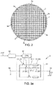
- the figure 2 illustrates a window which is constituted by a shielding assembly in accordance with the invention, and in which the two-dimensional structure 2 is a metal grid which extends over almost the entire useful surface of the substrate 1.
- This metal grid can be surrounded by a peripheral loop C, continuous and electrically conductive.
- This peripheral loop C can be formed on the substrate 1 in the same way as the metal grid of the two-dimensional structure 2, and possibly during the same steps of masking and material deposition processes.
- the peripheral loop C is then in electrical contact with the metal grid all around the latter.
- the device 3 may be advantageous for the device 3 to include several terminals 3a, for example six terminals 3a, which are distributed along the loop C to reduce differences between electrical resistances which are effective between any place of the two-dimensional structure 2 and each terminal 3b ( figure 1 ).
- the device 3 can have several terminals 3b which are arranged electrically in parallel with respect to each other, and which are intended to be electrically connected to different places of the shell part 101.
- the terminals 3b can be distributed and spaced approximately evenly along the mounting interface of the substrate 1 in the shell part 101.
- connection device electric 3 which are illustrated by the figures 3a and 3b , the variation of the electrical resistance of the device 3 is controlled electrically.
- the device 3 then comprises the microwave radiation detector 30, an electronic circuit 31, and a controller 32 denoted CTRL.
- the electronic circuit 31 comprises several branches 31-1, 31-2, ... which are connected in parallel between the terminals 3a and 3b.
- Each branch of the circuit 31 comprises an electrical resistance, referenced 31-1R for the branch 31-1, 31-2R for the branch 31-2, ... which is connected in series, inside this branch, with a switch, referenced 31-1C for branch 31-1, 31-2C for branch 31-2, etc.
- Each switch can be individually opened or closed by the controller 32, by means of a dedicated electrical control.
- the controller 32 receives from the detector 30 a signal which is representative of the intensity of the microwave radiation HYF.
- the open or closed state to be controlled for each level of the signal which is delivered by the detector 30, can be provided by a prerecorded table.
- the respective values of resistors 31-1 R, 31-2R, ... are selected as a function of the values of the shielding efficiency which are desired for several levels of intensity of the ultra-high frequency HYF radiation.
- the electrical resistance value which is produced by the device 3 then results from the parallel connection of the resistors 31-1R, 31-2R, ... branches whose switches 31-1C, 31-2C, ... are closed .
- the electronic circuit 31 comprises a component 31a of which an electrical resistance value which is effective for a microwave current, is variable as a function of a control voltage applied to this component 31a.
- the component 31a can be a PIN diode, commercially available, for example in the form of a discrete component, and where the acronym PIN denotes the type of diode to positively doped zone, intermediate layer with intrinsic conductivity, and negatively doped zone.
- the PIN diode 31a is connected between the two terminals 3a and 3b.
- Circuit 31 then comprises a DC and variable voltage source 31b, which is connected to PIN diode 31a to electrically bias the latter.
- the electrical resistance value of the PIN diode 31a which is effective for an alternating current at a frequency between 0.1 GHz and 40 GHz, called microwave current, can be adjusted by the bias voltage which is produced by the source 31b.
- the PIN diode 31a and the voltage source 31b are assembled in a loop, called a bias loop, which can further include a fixed resistor 31c.
- the controller 32 controls the bias voltage which is produced by the source 31b as a function of the microwave radiation intensity detection signal HYF, which is delivered by the detector 30.
- the microwave current which flows through the PIN diode 31a, between the two terminals 3a and 3b, is generated by the microwave radiation HYF which is incident on the two-dimensional structure 2.
- a decoupling capacitor 31d can also be inserted between the terminal 3a and the polarization loop.
- the PIN diode 31a can be replaced by a portion of a material with a metal-insulator transition as mentioned elsewhere in this description, when this portion is sensitive to a static electric field.
- the portion can be clamped between two electrodes, and in contact with them, the electrodes being electrically connected to the terminals 3a and 3b.
- the voltage source 31b then produces a static electric field in the portion of the metal-insulating transition material, on which depends the value of the electric resistance which is effective between the terminals 3a and 3b.
- the use of the detector 30 therefore makes it possible to adjust in real time, during the use of the detection system 100, the electrical resistance of the device 3 as a function of the intensity of the microwave radiation HYF. In the jargon of those skilled in the art, such an adjustment is said to be dynamic.
- the detector 30 can be omitted from the embodiments of the figures 3a and 3b .
- the controller 32 is then used initially to selectively open or close each of the switches 31-1C, 31-2C, ..., or to initially set the value of the electric voltage which is produced by the source 31b.
- the variation of the electrical resistance of the device 3 is thermally controlled.
- the device 3 then comprises the microwave radiation detector 30, a portion of a thermosensitive material 35, a thermal regulation means 36, and a controller 32 ′ denoted CTRL.
- the material of the portion 35 is selected to exhibit a metal-insulator transition, so that its electrical resistivity varies over a very wide amplitude as a function of the temperature. It can be a portion of vanadium dioxide (VO 2 ).
- the thermal regulation means 36 is for example a heating resistor or a Peltier effect element, or else a combination of the two in order to operate efficiently in cooling or in heating.
- thermosensitive material 35 It is placed in thermal contact with the portion of thermosensitive material 35, so as to control the temperature of the latter. It is thus possible, by means of detector 30 and controller 32 ', to control the electrical resistance of portion 35, and therefore that of device 3 between terminals 3a and 3b.
- the controller 32 ′ controls the operation of the thermal regulation means 36 as a function of the microwave radiation intensity detection signal HYF, which is delivered by the detector 30.
- the variation in the electrical resistance of the device 3 is produced by at least a portion 38 of a material which is directly sensitive to the intensity of the microwave radiation HYF.
- Each portion 38 is electrically connected between terminals 3a and 3b, and its material is selected to produce an electrical resistivity which depends on the intensity of the HYF microwave radiation which is received by this portion.
- the material of each portion 38 can be in particular vanadium dioxide (VO 2 ), for example with a thickness which is between 10 nm (nanometer) and 10 ⁇ m, measured perpendicular to the face of the substrate 1.
- VO 2 vanadium dioxide
- the materials with a metal-insulator transition already mentioned are also suitable for these third embodiments.
- each portion 38 must be exposed to the HYF microwave radiation.
- the two-dimensional structure for example a metal grid as described above, can be limited to the substrate 1 inside the peripheral loop C.
- the peripheral loop C is electrically conductive, also carried by the substrate 1 and connected electrically to the two-dimensional structure 2. Restricted zones can then be provided on the substrate 1, outside the peripheral loop C, between the latter and the peripheral edge of the substrate 1. Then, a portion 38 can be carried by the substrate 1 in each of these restricted areas, with a separate terminal 3b. In each zone, the portion 38 is electrically connected on one side to this terminal 3b, and on the other hand to the peripheral loop C.
- each portion 38 to one of the terminals 3b and to the peripheral loop C can be formed during the material deposition and etching steps used for the peripheral loop C and the two-dimensional structure 2.
- Each terminal 3a is then formed by the point or the segment of electrical connection of one of the portions 38 with the peripheral loop C.
- An advantage of such third embodiments of the invention is that the electrical connection device 3 with electrical resistance which is variable, is carried by the substrate 1 with the two-dimensional structure 2. Cost reduction and ease assembly within the detection system 100 result.
- the figure 3e illustrates a possible variant of the embodiment of the 3d figure .
- the substrate 1 For the sake of clarity and simplicity of the figure 3e , but without limitation as to all possible shapes for the substrate 1, the latter is shown with a peripheral edge which is square.
- the conductive peripheral loop C can then be parallel to this square edge.
- the two-dimensional conductive structure 2 can also be a metal grid as described above, but which comprises portions 38 of material sensitive to HYF microwave radiation, in the peripheral segments of this grid which connect it to the peripheral loop C. In this sense, the portions 38 constitute parts of the conductive two-dimensional structure 2.
- Each portion 38 therefore has a first end which is in electrical contact with the central part of the two-dimensional structure 2, and which constitutes a terminal 3a, and a second end which is in electrical contact with the peripheral loop C, and which constitutes a terminal 3b.
- the central part of the two-dimensional structure 2 can also have any configuration, in particular based on at least one thin metallic layer which is interposed between two dielectric layers, or based on at least one transparent conductive oxide layer, as indicated above, this (these) layer (s) can be continuous or possibly provided with recesses.
- the portions 38 of the metal-insulator transition material which is sensitive to microwave radiation by portions of a metal-insulator transition material which is sensitive to a static electric field (DC), or by diodes which are mounted on substrate 1, being connected to terminals 3a and 3b as indicated on these figures 3d and 3e .
- the diodes which are thus implemented can be of the PIN type mentioned above.
- the voltage source 31b is electrically connected between the central part of the metal grid which constitutes the two-dimensional conductive structure 2, and the peripheral loop C.
- the conductive two-dimensional structure 2 in a material with a metal-insulating transition which is sensitive to the intensity of the microwave radiation HYF. If this material is transparent for the RO optical radiation, it can continuously cover the face of the substrate 1 inside the peripheral loop C. Alternatively, if it is opaque for the RO optical radiation, the two-dimensional structure 2 can be a grid of this metal-insulating transition material which is sensitive to the intensity of HYF microwave radiation, which is carried by the substrate 1.
- electrical resistance values for device 3, to be produced for different levels of the intensity of the microwave radiation HYF, so as to obtain desired values for the shielding efficiency EB can be obtained.
- electrical resistance values for device 3, to be produced for different levels of the intensity of the microwave radiation HYF, so as to obtain desired values for the shielding efficiency EB can be obtained. be determined by experimental or empirical measurements, by parametric numerical simulations, or by theoretical models, without requiring any inventive step.
Applications Claiming Priority (2)
| Application Number | Priority Date | Filing Date | Title |
|---|---|---|---|
| FR1754537A FR3066645B1 (fr) | 2017-05-22 | 2017-05-22 | Ensemble de blindage electromagnetique transparent optiquement |
| PCT/EP2018/062529 WO2018215243A1 (fr) | 2017-05-22 | 2018-05-15 | Ensemble de blindage electromagnetique transparent optiquement |
Publications (2)
| Publication Number | Publication Date |
|---|---|
| EP3631392A1 EP3631392A1 (fr) | 2020-04-08 |
| EP3631392B1 true EP3631392B1 (fr) | 2021-03-03 |
Family
ID=62017311
Family Applications (1)
| Application Number | Title | Priority Date | Filing Date |
|---|---|---|---|
| EP18727710.8A Active EP3631392B1 (fr) | 2017-05-22 | 2018-05-15 | Ensemble de blindage electromagnetique transparent optiquement |
Country Status (9)
| Country | Link |
|---|---|
| US (1) | US11060920B2 (ja) |
| EP (1) | EP3631392B1 (ja) |
| JP (1) | JP6946469B2 (ja) |
| KR (1) | KR102303505B1 (ja) |
| CN (1) | CN111512130B (ja) |
| CA (1) | CA3064462A1 (ja) |
| FR (1) | FR3066645B1 (ja) |
| IL (1) | IL270725B (ja) |
| WO (1) | WO2018215243A1 (ja) |
Families Citing this family (4)
| Publication number | Priority date | Publication date | Assignee | Title |
|---|---|---|---|---|
| KR102363436B1 (ko) | 2020-07-14 | 2022-02-15 | 주식회사 엠아이이큅먼트코리아 | 반도체 칩의 레이저 컴프레션 본딩장치 및 본딩방법 |
| FR3112898B1 (fr) * | 2020-07-22 | 2022-07-01 | Safran Electronics & Defense | Ensemble de blindage electromagnetique transparent optiquement |
| FR3120697B1 (fr) | 2021-03-11 | 2023-03-31 | Centre Nat Rech Scient | Systeme de commande pour ecran de blindage actif |
| FR3128783B1 (fr) | 2021-10-28 | 2023-10-06 | Centre Nat Rech Scient | Ecran de blindage electromagnetique auto-adaptatif a couches minces |
Family Cites Families (19)
| Publication number | Priority date | Publication date | Assignee | Title |
|---|---|---|---|---|
| US5783805A (en) * | 1992-06-05 | 1998-07-21 | Katzmann; Fred L. | Electrothermal conversion elements, apparatus and methods for use in comparing, calibrating and measuring electrical signals |
| CA2356992C (en) * | 1999-01-25 | 2007-09-18 | Gentex Corporation | Vehicle equipment control with semiconductor light sensors |
| US6815220B2 (en) * | 1999-11-23 | 2004-11-09 | Intel Corporation | Magnetic layer processing |
| JP2001210990A (ja) * | 2000-01-28 | 2001-08-03 | Takenaka Komuten Co Ltd | 電波遮蔽制御体とこれを用いてのシールド対象周波数可変の電磁波シールドシステム |
| JP3835525B2 (ja) | 2001-03-19 | 2006-10-18 | ホーチキ株式会社 | 波長可変フィルタ制御装置 |
| JP2003194630A (ja) * | 2001-12-27 | 2003-07-09 | Ishizuka Electronics Corp | 非接触温度センサおよび非接触温度センサ用検出回路 |
| US7543946B2 (en) * | 2002-01-10 | 2009-06-09 | Gentex Corporation | Dimmable rearview assembly having a glare sensor |
| JP2005309099A (ja) | 2004-04-21 | 2005-11-04 | Seiko Epson Corp | 波長可変フィルタ及びその製造方法 |
| KR100682996B1 (ko) * | 2005-05-17 | 2007-02-15 | 한국전자통신연구원 | 단일 주파수 대역 필터링을 위한 fss 구조 |
| WO2006098333A1 (ja) * | 2005-03-15 | 2006-09-21 | Fujifilm Corporation | 透光性導電性膜及び透光性導電性膜の製造方法 |
| JP4812119B2 (ja) * | 2007-04-27 | 2011-11-09 | 独立行政法人情報通信研究機構 | 電波シャッター |
| JP4818224B2 (ja) | 2007-08-09 | 2011-11-16 | 株式会社東芝 | 可変抵抗器及びこれを用いたフィルタ、可変利得増幅器及び集積回路 |
| US8098079B2 (en) * | 2009-04-17 | 2012-01-17 | Oracle America, Inc. | Receive circuit for connectors with variable complex impedance |
| US20120037803A1 (en) * | 2010-08-12 | 2012-02-16 | Flir Systems, Inc. | Electromagnetic interference shield |
| KR101299675B1 (ko) * | 2012-02-07 | 2013-08-27 | 공주대학교 산학협력단 | 주파수 특성 가변 fss 필터 |
| US9589904B2 (en) * | 2013-02-14 | 2017-03-07 | Infineon Technologies Austria Ag | Semiconductor device with bypass functionality and method thereof |
| CN104576616B (zh) * | 2013-10-14 | 2017-10-17 | 纮华电子科技(上海)有限公司 | 模块集成电路封装结构及其制作方法 |
| WO2015199624A1 (en) * | 2014-06-23 | 2015-12-30 | Aselsan Elektronik Sanayi Ve Ticaret Anonim Şirketi | A graphene based emi shielding optical coating |
| CN106571424B (zh) * | 2016-11-04 | 2019-09-24 | 北京有色金属研究总院 | 一种抗电磁干扰的阻变存储器及其制备方法 |
-
2017
- 2017-05-22 FR FR1754537A patent/FR3066645B1/fr not_active Expired - Fee Related
-
2018
- 2018-05-15 KR KR1020197034644A patent/KR102303505B1/ko active IP Right Grant
- 2018-05-15 CA CA3064462A patent/CA3064462A1/fr active Pending
- 2018-05-15 US US16/615,265 patent/US11060920B2/en active Active
- 2018-05-15 EP EP18727710.8A patent/EP3631392B1/fr active Active
- 2018-05-15 CN CN201880049225.2A patent/CN111512130B/zh active Active
- 2018-05-15 WO PCT/EP2018/062529 patent/WO2018215243A1/fr active Application Filing
- 2018-05-15 JP JP2019564496A patent/JP6946469B2/ja active Active
-
2019
- 2019-11-18 IL IL270725A patent/IL270725B/en active IP Right Grant
Non-Patent Citations (1)
| Title |
|---|
| None * |
Also Published As
| Publication number | Publication date |
|---|---|
| JP2020521136A (ja) | 2020-07-16 |
| CA3064462A1 (fr) | 2018-11-29 |
| IL270725B (en) | 2020-07-30 |
| FR3066645B1 (fr) | 2019-06-21 |
| KR102303505B1 (ko) | 2021-09-23 |
| CN111512130B (zh) | 2021-07-27 |
| US11060920B2 (en) | 2021-07-13 |
| JP6946469B2 (ja) | 2021-10-06 |
| KR20200087077A (ko) | 2020-07-20 |
| CN111512130A (zh) | 2020-08-07 |
| FR3066645A1 (fr) | 2018-11-23 |
| US20200173859A1 (en) | 2020-06-04 |
| WO2018215243A1 (fr) | 2018-11-29 |
| IL270725A (en) | 2020-01-30 |
| EP3631392A1 (fr) | 2020-04-08 |
Similar Documents
| Publication | Publication Date | Title |
|---|---|---|
| EP3631392B1 (fr) | Ensemble de blindage electromagnetique transparent optiquement | |
| EP1721136B1 (fr) | Procede de realisation d'un dispositif pour la detection thermique d'un rayonnement comportant un microbolometre actif et un microbolometre passif | |
| WO2005011052A2 (fr) | Substrat avec un revetement electriquement conducteur et une fenetre de communication | |
| FR2977937A1 (fr) | Detecteur bolometrique a performances ameliorees | |
| EP1715315A1 (fr) | Détecteur bolométrique, dispositif de détection d'ondes électromagnétiques submillimétriques et millimétriques mettant en oeuvre un tel détecteur | |
| FR3033422A1 (fr) | Afficheur avec systeme de transfert d'images | |
| FR2930374A1 (fr) | Circulateur radiofrequence a base de mems. | |
| EP2840370A1 (fr) | Détecteur bolométrique à bolométre de compensation à thermalisation renforcée | |
| EP3782790B1 (fr) | Procédé pour pièce de carrosserie comportant un film chauffant | |
| EP3205180B1 (fr) | Vitrage chauffant et de blindage electromagnetique | |
| FR2875336A1 (fr) | Dispositif de detection de rayonnements infrarouges a detecteurs bolometriques | |
| CA3025328C (fr) | Element de blindage electromagnetique optiquement transparent et a plusieurs zones | |
| EP4186103B1 (fr) | Ensemble de blindage électromagnétique transparent optiquement | |
| FR2845157A1 (fr) | Detecteur bolometrique a antenne comportant un interrupteur et dispositif d'imagerie le comportant. | |
| FR2779889A1 (fr) | Detecteur de contact par effet capacitif | |
| EP0024970B1 (fr) | Procédé de fabrication d'un dispositif photodétecteur à semiconducteur | |
| EP3772133B1 (fr) | Dispositif de protection pour lidar de véhicule automobile | |
| FR3128783A1 (fr) | Ecran de blindage electromagnetique auto-adaptatif a couches minces | |
| FR3064062A1 (fr) | Detecteur pyroelectrique | |
| WO2024079259A1 (fr) | Unité de protection et ensemble de détection pour véhicule automobile | |
| FR3066017A1 (fr) | Dispositif pyroelectrique de detection infrarouge comportant un emetteur infrarouge de modulation | |
| WO2019043312A1 (fr) | Detecteur de rayonnement electromagnetique | |
| FR2748889A1 (fr) | Protection des circuits electroniques a bord d'un missile contre les parasites electromagnetiques | |
| FR2673775A1 (fr) | Composant pour la protection contre les surcharges electriques et procede de fabrication. |
Legal Events
| Date | Code | Title | Description |
|---|---|---|---|
| STAA | Information on the status of an ep patent application or granted ep patent |
Free format text: STATUS: UNKNOWN |
|
| STAA | Information on the status of an ep patent application or granted ep patent |
Free format text: STATUS: THE INTERNATIONAL PUBLICATION HAS BEEN MADE |
|
| PUAI | Public reference made under article 153(3) epc to a published international application that has entered the european phase |
Free format text: ORIGINAL CODE: 0009012 |
|
| STAA | Information on the status of an ep patent application or granted ep patent |
Free format text: STATUS: REQUEST FOR EXAMINATION WAS MADE |
|
| 17P | Request for examination filed |
Effective date: 20191120 |
|
| AK | Designated contracting states |
Kind code of ref document: A1 Designated state(s): AL AT BE BG CH CY CZ DE DK EE ES FI FR GB GR HR HU IE IS IT LI LT LU LV MC MK MT NL NO PL PT RO RS SE SI SK SM TR |
|
| AX | Request for extension of the european patent |
Extension state: BA ME |
|
| DAV | Request for validation of the european patent (deleted) | ||
| DAX | Request for extension of the european patent (deleted) | ||
| GRAP | Despatch of communication of intention to grant a patent |
Free format text: ORIGINAL CODE: EPIDOSNIGR1 |
|
| STAA | Information on the status of an ep patent application or granted ep patent |
Free format text: STATUS: GRANT OF PATENT IS INTENDED |
|
| INTG | Intention to grant announced |
Effective date: 20201211 |
|
| GRAS | Grant fee paid |
Free format text: ORIGINAL CODE: EPIDOSNIGR3 |
|
| STAA | Information on the status of an ep patent application or granted ep patent |
Free format text: STATUS: GRANT OF PATENT IS INTENDED |
|
| GRAA | (expected) grant |
Free format text: ORIGINAL CODE: 0009210 |
|
| STAA | Information on the status of an ep patent application or granted ep patent |
Free format text: STATUS: THE PATENT HAS BEEN GRANTED |
|
| AK | Designated contracting states |
Kind code of ref document: B1 Designated state(s): AL AT BE BG CH CY CZ DE DK EE ES FI FR GB GR HR HU IE IS IT LI LT LU LV MC MK MT NL NO PL PT RO RS SE SI SK SM TR |
|
| REG | Reference to a national code |
Ref country code: GB Ref legal event code: FG4D Free format text: NOT ENGLISH |
|
| REG | Reference to a national code |
Ref country code: AT Ref legal event code: REF Ref document number: 1367704 Country of ref document: AT Kind code of ref document: T Effective date: 20210315 Ref country code: CH Ref legal event code: EP |
|
| REG | Reference to a national code |
Ref country code: DE Ref legal event code: R096 Ref document number: 602018013440 Country of ref document: DE |
|
| REG | Reference to a national code |
Ref country code: IE Ref legal event code: FG4D Free format text: LANGUAGE OF EP DOCUMENT: FRENCH |
|
| REG | Reference to a national code |
Ref country code: SE Ref legal event code: TRGR |
|
| REG | Reference to a national code |
Ref country code: LT Ref legal event code: MG9D |
|
| PG25 | Lapsed in a contracting state [announced via postgrant information from national office to epo] |
Ref country code: BG Free format text: LAPSE BECAUSE OF FAILURE TO SUBMIT A TRANSLATION OF THE DESCRIPTION OR TO PAY THE FEE WITHIN THE PRESCRIBED TIME-LIMIT Effective date: 20210603 Ref country code: GR Free format text: LAPSE BECAUSE OF FAILURE TO SUBMIT A TRANSLATION OF THE DESCRIPTION OR TO PAY THE FEE WITHIN THE PRESCRIBED TIME-LIMIT Effective date: 20210604 Ref country code: HR Free format text: LAPSE BECAUSE OF FAILURE TO SUBMIT A TRANSLATION OF THE DESCRIPTION OR TO PAY THE FEE WITHIN THE PRESCRIBED TIME-LIMIT Effective date: 20210303 Ref country code: FI Free format text: LAPSE BECAUSE OF FAILURE TO SUBMIT A TRANSLATION OF THE DESCRIPTION OR TO PAY THE FEE WITHIN THE PRESCRIBED TIME-LIMIT Effective date: 20210303 Ref country code: NO Free format text: LAPSE BECAUSE OF FAILURE TO SUBMIT A TRANSLATION OF THE DESCRIPTION OR TO PAY THE FEE WITHIN THE PRESCRIBED TIME-LIMIT Effective date: 20210603 Ref country code: LT Free format text: LAPSE BECAUSE OF FAILURE TO SUBMIT A TRANSLATION OF THE DESCRIPTION OR TO PAY THE FEE WITHIN THE PRESCRIBED TIME-LIMIT Effective date: 20210303 |
|
| REG | Reference to a national code |
Ref country code: NL Ref legal event code: MP Effective date: 20210303 |
|
| REG | Reference to a national code |
Ref country code: AT Ref legal event code: MK05 Ref document number: 1367704 Country of ref document: AT Kind code of ref document: T Effective date: 20210303 |
|
| PG25 | Lapsed in a contracting state [announced via postgrant information from national office to epo] |
Ref country code: LV Free format text: LAPSE BECAUSE OF FAILURE TO SUBMIT A TRANSLATION OF THE DESCRIPTION OR TO PAY THE FEE WITHIN THE PRESCRIBED TIME-LIMIT Effective date: 20210303 Ref country code: RS Free format text: LAPSE BECAUSE OF FAILURE TO SUBMIT A TRANSLATION OF THE DESCRIPTION OR TO PAY THE FEE WITHIN THE PRESCRIBED TIME-LIMIT Effective date: 20210303 Ref country code: PL Free format text: LAPSE BECAUSE OF FAILURE TO SUBMIT A TRANSLATION OF THE DESCRIPTION OR TO PAY THE FEE WITHIN THE PRESCRIBED TIME-LIMIT Effective date: 20210303 |
|
| PG25 | Lapsed in a contracting state [announced via postgrant information from national office to epo] |
Ref country code: NL Free format text: LAPSE BECAUSE OF FAILURE TO SUBMIT A TRANSLATION OF THE DESCRIPTION OR TO PAY THE FEE WITHIN THE PRESCRIBED TIME-LIMIT Effective date: 20210303 |
|
| PG25 | Lapsed in a contracting state [announced via postgrant information from national office to epo] |
Ref country code: AT Free format text: LAPSE BECAUSE OF FAILURE TO SUBMIT A TRANSLATION OF THE DESCRIPTION OR TO PAY THE FEE WITHIN THE PRESCRIBED TIME-LIMIT Effective date: 20210303 Ref country code: SM Free format text: LAPSE BECAUSE OF FAILURE TO SUBMIT A TRANSLATION OF THE DESCRIPTION OR TO PAY THE FEE WITHIN THE PRESCRIBED TIME-LIMIT Effective date: 20210303 Ref country code: CZ Free format text: LAPSE BECAUSE OF FAILURE TO SUBMIT A TRANSLATION OF THE DESCRIPTION OR TO PAY THE FEE WITHIN THE PRESCRIBED TIME-LIMIT Effective date: 20210303 Ref country code: EE Free format text: LAPSE BECAUSE OF FAILURE TO SUBMIT A TRANSLATION OF THE DESCRIPTION OR TO PAY THE FEE WITHIN THE PRESCRIBED TIME-LIMIT Effective date: 20210303 |
|
| PG25 | Lapsed in a contracting state [announced via postgrant information from national office to epo] |
Ref country code: IS Free format text: LAPSE BECAUSE OF FAILURE TO SUBMIT A TRANSLATION OF THE DESCRIPTION OR TO PAY THE FEE WITHIN THE PRESCRIBED TIME-LIMIT Effective date: 20210703 Ref country code: PT Free format text: LAPSE BECAUSE OF FAILURE TO SUBMIT A TRANSLATION OF THE DESCRIPTION OR TO PAY THE FEE WITHIN THE PRESCRIBED TIME-LIMIT Effective date: 20210705 Ref country code: RO Free format text: LAPSE BECAUSE OF FAILURE TO SUBMIT A TRANSLATION OF THE DESCRIPTION OR TO PAY THE FEE WITHIN THE PRESCRIBED TIME-LIMIT Effective date: 20210303 Ref country code: SK Free format text: LAPSE BECAUSE OF FAILURE TO SUBMIT A TRANSLATION OF THE DESCRIPTION OR TO PAY THE FEE WITHIN THE PRESCRIBED TIME-LIMIT Effective date: 20210303 |
|
| REG | Reference to a national code |
Ref country code: DE Ref legal event code: R097 Ref document number: 602018013440 Country of ref document: DE |
|
| REG | Reference to a national code |
Ref country code: CH Ref legal event code: PL |
|
| PLBE | No opposition filed within time limit |
Free format text: ORIGINAL CODE: 0009261 |
|
| STAA | Information on the status of an ep patent application or granted ep patent |
Free format text: STATUS: NO OPPOSITION FILED WITHIN TIME LIMIT |
|
| PG25 | Lapsed in a contracting state [announced via postgrant information from national office to epo] |
Ref country code: ES Free format text: LAPSE BECAUSE OF FAILURE TO SUBMIT A TRANSLATION OF THE DESCRIPTION OR TO PAY THE FEE WITHIN THE PRESCRIBED TIME-LIMIT Effective date: 20210303 Ref country code: DK Free format text: LAPSE BECAUSE OF FAILURE TO SUBMIT A TRANSLATION OF THE DESCRIPTION OR TO PAY THE FEE WITHIN THE PRESCRIBED TIME-LIMIT Effective date: 20210303 Ref country code: CH Free format text: LAPSE BECAUSE OF NON-PAYMENT OF DUE FEES Effective date: 20210531 Ref country code: AL Free format text: LAPSE BECAUSE OF FAILURE TO SUBMIT A TRANSLATION OF THE DESCRIPTION OR TO PAY THE FEE WITHIN THE PRESCRIBED TIME-LIMIT Effective date: 20210303 Ref country code: LI Free format text: LAPSE BECAUSE OF NON-PAYMENT OF DUE FEES Effective date: 20210531 Ref country code: MC Free format text: LAPSE BECAUSE OF FAILURE TO SUBMIT A TRANSLATION OF THE DESCRIPTION OR TO PAY THE FEE WITHIN THE PRESCRIBED TIME-LIMIT Effective date: 20210303 Ref country code: LU Free format text: LAPSE BECAUSE OF NON-PAYMENT OF DUE FEES Effective date: 20210515 |
|
| 26N | No opposition filed |
Effective date: 20211206 |
|
| REG | Reference to a national code |
Ref country code: BE Ref legal event code: MM Effective date: 20210531 |
|
| PG25 | Lapsed in a contracting state [announced via postgrant information from national office to epo] |
Ref country code: SI Free format text: LAPSE BECAUSE OF FAILURE TO SUBMIT A TRANSLATION OF THE DESCRIPTION OR TO PAY THE FEE WITHIN THE PRESCRIBED TIME-LIMIT Effective date: 20210303 |
|
| PG25 | Lapsed in a contracting state [announced via postgrant information from national office to epo] |
Ref country code: IE Free format text: LAPSE BECAUSE OF NON-PAYMENT OF DUE FEES Effective date: 20210515 |
|
| PG25 | Lapsed in a contracting state [announced via postgrant information from national office to epo] |
Ref country code: IS Free format text: LAPSE BECAUSE OF FAILURE TO SUBMIT A TRANSLATION OF THE DESCRIPTION OR TO PAY THE FEE WITHIN THE PRESCRIBED TIME-LIMIT Effective date: 20210703 |
|
| PG25 | Lapsed in a contracting state [announced via postgrant information from national office to epo] |
Ref country code: BE Free format text: LAPSE BECAUSE OF NON-PAYMENT OF DUE FEES Effective date: 20210531 |
|
| PG25 | Lapsed in a contracting state [announced via postgrant information from national office to epo] |
Ref country code: CY Free format text: LAPSE BECAUSE OF FAILURE TO SUBMIT A TRANSLATION OF THE DESCRIPTION OR TO PAY THE FEE WITHIN THE PRESCRIBED TIME-LIMIT Effective date: 20210303 |
|
| PG25 | Lapsed in a contracting state [announced via postgrant information from national office to epo] |
Ref country code: HU Free format text: LAPSE BECAUSE OF FAILURE TO SUBMIT A TRANSLATION OF THE DESCRIPTION OR TO PAY THE FEE WITHIN THE PRESCRIBED TIME-LIMIT; INVALID AB INITIO Effective date: 20180515 |
|
| PGFP | Annual fee paid to national office [announced via postgrant information from national office to epo] |
Ref country code: IT Payment date: 20230420 Year of fee payment: 6 Ref country code: FR Payment date: 20230420 Year of fee payment: 6 Ref country code: DE Payment date: 20230419 Year of fee payment: 6 |
|
| PGFP | Annual fee paid to national office [announced via postgrant information from national office to epo] |
Ref country code: SE Payment date: 20230419 Year of fee payment: 6 |
|
| PGFP | Annual fee paid to national office [announced via postgrant information from national office to epo] |
Ref country code: GB Payment date: 20230420 Year of fee payment: 6 |