EP3627705A1 - Appareils pour générer un signal d'oscillation - Google Patents
Appareils pour générer un signal d'oscillation Download PDFInfo
- Publication number
- EP3627705A1 EP3627705A1 EP18195839.8A EP18195839A EP3627705A1 EP 3627705 A1 EP3627705 A1 EP 3627705A1 EP 18195839 A EP18195839 A EP 18195839A EP 3627705 A1 EP3627705 A1 EP 3627705A1
- Authority
- EP
- European Patent Office
- Prior art keywords
- oscillation signal
- reference oscillation
- frequency
- oscillator
- generate
- Prior art date
- Legal status (The legal status is an assumption and is not a legal conclusion. Google has not performed a legal analysis and makes no representation as to the accuracy of the status listed.)
- Withdrawn
Links
- 230000010355 oscillation Effects 0.000 title claims abstract description 257
- 238000012545 processing Methods 0.000 claims abstract description 16
- 238000005070 sampling Methods 0.000 claims description 10
- 238000000034 method Methods 0.000 description 14
- 238000004891 communication Methods 0.000 description 6
- 230000008569 process Effects 0.000 description 6
- 238000006243 chemical reaction Methods 0.000 description 5
- 239000013078 crystal Substances 0.000 description 5
- 230000007274 generation of a signal involved in cell-cell signaling Effects 0.000 description 5
- 230000001419 dependent effect Effects 0.000 description 4
- 238000010586 diagram Methods 0.000 description 4
- 230000001747 exhibiting effect Effects 0.000 description 4
- 230000006870 function Effects 0.000 description 4
- 238000010295 mobile communication Methods 0.000 description 4
- 230000010363 phase shift Effects 0.000 description 3
- 239000004065 semiconductor Substances 0.000 description 3
- 238000001228 spectrum Methods 0.000 description 3
- 230000007480 spreading Effects 0.000 description 3
- 239000000872 buffer Substances 0.000 description 2
- 239000003990 capacitor Substances 0.000 description 2
- 230000000694 effects Effects 0.000 description 2
- 238000001914 filtration Methods 0.000 description 2
- 230000000116 mitigating effect Effects 0.000 description 2
- 238000012986 modification Methods 0.000 description 2
- 230000004048 modification Effects 0.000 description 2
- 230000010356 wave oscillation Effects 0.000 description 2
- 230000018199 S phase Effects 0.000 description 1
- 230000015572 biosynthetic process Effects 0.000 description 1
- 238000012937 correction Methods 0.000 description 1
- 230000007774 longterm Effects 0.000 description 1
- 238000007493 shaping process Methods 0.000 description 1
- 238000003786 synthesis reaction Methods 0.000 description 1
- 230000007704 transition Effects 0.000 description 1
Images


Classifications
-
- H—ELECTRICITY
- H03—ELECTRONIC CIRCUITRY
- H03L—AUTOMATIC CONTROL, STARTING, SYNCHRONISATION OR STABILISATION OF GENERATORS OF ELECTRONIC OSCILLATIONS OR PULSES
- H03L7/00—Automatic control of frequency or phase; Synchronisation
- H03L7/06—Automatic control of frequency or phase; Synchronisation using a reference signal applied to a frequency- or phase-locked loop
- H03L7/08—Details of the phase-locked loop
- H03L7/099—Details of the phase-locked loop concerning mainly the controlled oscillator of the loop
- H03L7/0991—Details of the phase-locked loop concerning mainly the controlled oscillator of the loop the oscillator being a digital oscillator, e.g. composed of a fixed oscillator followed by a variable frequency divider
- H03L7/0992—Details of the phase-locked loop concerning mainly the controlled oscillator of the loop the oscillator being a digital oscillator, e.g. composed of a fixed oscillator followed by a variable frequency divider comprising a counter or a frequency divider
-
- H—ELECTRICITY
- H03—ELECTRONIC CIRCUITRY
- H03L—AUTOMATIC CONTROL, STARTING, SYNCHRONISATION OR STABILISATION OF GENERATORS OF ELECTRONIC OSCILLATIONS OR PULSES
- H03L7/00—Automatic control of frequency or phase; Synchronisation
- H03L7/06—Automatic control of frequency or phase; Synchronisation using a reference signal applied to a frequency- or phase-locked loop
- H03L7/07—Automatic control of frequency or phase; Synchronisation using a reference signal applied to a frequency- or phase-locked loop using several loops, e.g. for redundant clock signal generation
-
- H—ELECTRICITY
- H03—ELECTRONIC CIRCUITRY
- H03B—GENERATION OF OSCILLATIONS, DIRECTLY OR BY FREQUENCY-CHANGING, BY CIRCUITS EMPLOYING ACTIVE ELEMENTS WHICH OPERATE IN A NON-SWITCHING MANNER; GENERATION OF NOISE BY SUCH CIRCUITS
- H03B5/00—Generation of oscillations using amplifier with regenerative feedback from output to input
- H03B5/30—Generation of oscillations using amplifier with regenerative feedback from output to input with frequency-determining element being electromechanical resonator
- H03B5/32—Generation of oscillations using amplifier with regenerative feedback from output to input with frequency-determining element being electromechanical resonator being a piezoelectric resonator
-
- H—ELECTRICITY
- H03—ELECTRONIC CIRCUITRY
- H03L—AUTOMATIC CONTROL, STARTING, SYNCHRONISATION OR STABILISATION OF GENERATORS OF ELECTRONIC OSCILLATIONS OR PULSES
- H03L7/00—Automatic control of frequency or phase; Synchronisation
- H03L7/06—Automatic control of frequency or phase; Synchronisation using a reference signal applied to a frequency- or phase-locked loop
- H03L7/08—Details of the phase-locked loop
- H03L7/081—Details of the phase-locked loop provided with an additional controlled phase shifter
- H03L7/0812—Details of the phase-locked loop provided with an additional controlled phase shifter and where no voltage or current controlled oscillator is used
- H03L7/0814—Details of the phase-locked loop provided with an additional controlled phase shifter and where no voltage or current controlled oscillator is used the phase shifting device being digitally controlled
-
- H—ELECTRICITY
- H03—ELECTRONIC CIRCUITRY
- H03L—AUTOMATIC CONTROL, STARTING, SYNCHRONISATION OR STABILISATION OF GENERATORS OF ELECTRONIC OSCILLATIONS OR PULSES
- H03L7/00—Automatic control of frequency or phase; Synchronisation
- H03L7/06—Automatic control of frequency or phase; Synchronisation using a reference signal applied to a frequency- or phase-locked loop
- H03L7/08—Details of the phase-locked loop
- H03L7/085—Details of the phase-locked loop concerning mainly the frequency- or phase-detection arrangement including the filtering or amplification of its output signal
- H03L7/091—Details of the phase-locked loop concerning mainly the frequency- or phase-detection arrangement including the filtering or amplification of its output signal the phase or frequency detector using a sampling device
-
- H—ELECTRICITY
- H03—ELECTRONIC CIRCUITRY
- H03L—AUTOMATIC CONTROL, STARTING, SYNCHRONISATION OR STABILISATION OF GENERATORS OF ELECTRONIC OSCILLATIONS OR PULSES
- H03L7/00—Automatic control of frequency or phase; Synchronisation
- H03L7/06—Automatic control of frequency or phase; Synchronisation using a reference signal applied to a frequency- or phase-locked loop
- H03L7/16—Indirect frequency synthesis, i.e. generating a desired one of a number of predetermined frequencies using a frequency- or phase-locked loop
- H03L7/22—Indirect frequency synthesis, i.e. generating a desired one of a number of predetermined frequencies using a frequency- or phase-locked loop using more than one loop
- H03L7/23—Indirect frequency synthesis, i.e. generating a desired one of a number of predetermined frequencies using a frequency- or phase-locked loop using more than one loop with pulse counters or frequency dividers
-
- H—ELECTRICITY
- H04—ELECTRIC COMMUNICATION TECHNIQUE
- H04B—TRANSMISSION
- H04B1/00—Details of transmission systems, not covered by a single one of groups H04B3/00 - H04B13/00; Details of transmission systems not characterised by the medium used for transmission
- H04B1/02—Transmitters
- H04B1/04—Circuits
-
- H—ELECTRICITY
- H03—ELECTRONIC CIRCUITRY
- H03L—AUTOMATIC CONTROL, STARTING, SYNCHRONISATION OR STABILISATION OF GENERATORS OF ELECTRONIC OSCILLATIONS OR PULSES
- H03L2207/00—Indexing scheme relating to automatic control of frequency or phase and to synchronisation
- H03L2207/50—All digital phase-locked loop
-
- H—ELECTRICITY
- H04—ELECTRIC COMMUNICATION TECHNIQUE
- H04B—TRANSMISSION
- H04B1/00—Details of transmission systems, not covered by a single one of groups H04B3/00 - H04B13/00; Details of transmission systems not characterised by the medium used for transmission
- H04B1/02—Transmitters
- H04B1/04—Circuits
- H04B2001/0491—Circuits with frequency synthesizers, frequency converters or modulators
Definitions
- the present disclosure relates to oscillation signal generation.
- examples relate to apparatuses for generating an oscillation signal.
- Further examples relate to a transmitter, a receiver, a mobile device and a semiconductor die comprising at least one of the apparatuses for generating an oscillation signal.
- Phase noise requirements for oscillation signals are getting tougher with each new communication standard. At the same time, low power consumption of the circuitry generating the oscillation signal is desired.
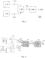
- Fig. 1 illustrates an apparatus 100 for generating an oscillation signal 101.
- the apparatus 100 comprises a first oscillator 110 configured to generate a first reference oscillation signal 101, and second oscillator 120 configured to generate a second reference oscillation signal 121.
- a frequency accuracy of the first oscillator 110 is higher (better) than a frequency accuracy of the second oscillator 120.
- an oscillator phase noise of the second oscillator 120 is lower than an oscillator phase noise of the first oscillator 110.
- the frequency accuracy of the first oscillator 110 may be at least ten, hundred, thousand times higher than the frequency accuracy of the second oscillator 120.
- the second oscillator 120 may, e.g., comprises a high quality (high Q) resonator.
- the first oscillation signal 111 exhibits a high frequency accuracy (e.g. vs. Process, Voltage and Temperature, PVT, variations) while the second oscillation signal 121 exhibits low phase noise.
- the apparatus 100 further comprises a processing circuit 130 configured to generate a third reference oscillation signal 131 based on the first reference oscillation signal 111 and the second reference oscillation signal 121.
- the processing circuit 130 may generate the third reference oscillation signal 131 at high frequency and high quality.
- the third reference oscillation signal 131 may exhibit a high frequency accuracy and a low level of phase noise.
- the frequency of the third reference oscillation signal 131 is higher than a frequency of the first reference oscillation signal 111.
- the frequency of the third reference oscillation signal 131 may be at least 200, 400, 600, 800 or 1000 MHz.
- the apparatus 100 comprises Phase-Locked Loop (PLL) 140 configured to generate the oscillation signal 101 based on the third reference oscillation signal 131.
- the frequency of the oscillation signal 101 is a multiple of the frequency of the third reference oscillation signal 131.
- the third reference oscillation signal 131 may be understood as a high frequency, high quality reference for the PLL 140.
- the PLL 140 may be an Analog PLL (APLL) or a Digital PLL (DPLL).
- the frequency of the oscillation signal 101 may be an integer or a fractional multiple of the frequency of the third reference oscillation signal 131. In other words, the PLL 140 may be an integer PLL or a fractional PLL.
- an integer-N DPLL (iDPLL) exhibiting a configurable output frequency may be used together with the configurable third reference oscillation signal 131. Due to its limited bandwidth, the PLL 140 may further allow to filter or reduce spurs present in the third reference oscillation signal 131.
- a bandwidth of the PLL 140 may be less than 50, 40, 30, 20 or 10 MHz (i.e. less than ⁇ 25, ⁇ 20, ⁇ 15, ⁇ 10 or ⁇ 5 MHz).
- the use of the PLL 140 together with the high frequency, high quality reference 131 may allow to generate the oscillation signal 101 with (very) low phase noise, low (reduced) spurs at low power consumption.
- FIG. 2 Another apparatus 200 for generating the oscillation signal 101 is illustrated in Fig. 2 .
- FIG. 2 Another apparatus 200 for generating the oscillation signal 101 is illustrated in Fig. 2 .
- FIG. 2 Another apparatus 200 for generating the oscillation signal 101 is illustrated in Fig. 2 .
- FIG. 2 Another apparatus 200 for generating the oscillation signal 101 is illustrated in Fig. 2 .
- FIG. 1 Another apparatus 200 for generating the oscillation signal 101 is illustrated in comparison to the apparatus 100 illustrated in Fig. 1 , more details of the first oscillator 110 and the second oscillator 120 are illustrated.
- the first oscillator 110 comprises a first resonator 112 and further oscillator circuitry 113 (e.g. load capacitors, buffers, voltage supply etc.).
- the first resonator 112 exhibits high frequency accuracy.
- the first resonator 112 may be a crystal resonator as indicated in Fig. 2 .
- a crystal resonator may, e.g., provide oscillation signals having their first harmonic at frequencies of less than 100 MHz.
- the first resonator 112 may be a MicroElectroMechanical System (MEMS) resonator, a piezoelectric resonator, an electrostatic resonator or a printed resonator.
- the first reference oscillation signal 111 of the first oscillator 110 serves as high frequency accuracy reference.
- the second oscillator 120 comprises a second resonator 122 and further oscillator circuitry 123 (e.g. load capacitors, buffers, voltage supply etc.).
- the second resonator 122 as well as the other circuitry of the second oscillator provide low phase noise to the second reference oscillation signal 121.
- the second resonator 122 may be a high Q resonator.
- This signal is feed as high frequency, high quality reference to the iDPLL 140.
- M is an adjustable integer.
- the specific use of the optimized iDPLL 140 together with the high frequency, high quality reference 131 may allow to achieve very low phase noise and reduced spurs in the oscillation signal 101.
- the apparatus 200 may allow generation of the oscillation signal 101 at low power consumption.
- a further apparatus 300 for generating the oscillation signal 101 is illustrated in Fig. 3 .
- the apparatus 300 illustrates further details of the processing circuit 130 and the PLL 140.
- the apparatus 300 again uses two reference sources.
- the second oscillator 120 is used as a high Q reference source that generates the second reference oscillation signal 121 for clocking a phase shifter circuit 132 of the processing circuit 130.
- the phase shifter circuit 132 may, e.g., be a Digital-to-Time Converter (DTC) configured to receive the second reference oscillation signal 121 at a clock input terminal.
- DTC Digital-to-Time Converter
- the first oscillator 110 is used as an accurate but low quality reference that generate the first reference oscillation signal 111 for estimating the frequency of the third reference oscillation signal 131.
- the phase shifter circuit 132 is configured to generate the third reference oscillation signal 131 based on the second reference oscillation signal 121 and a control word 134.
- a control circuit 133 of the processing circuit 130 is configured to determine a frequency shift of the third reference oscillation signal 131 with respect to the first reference oscillation signal 111, which exhibits high frequency accuracy. Further, the control circuit 133 is configured to generate the control word 134 based on the frequency shift. Due to the low phase noise of the second reference oscillation signal 121, the third reference oscillation signal exhibits very low jitter.
- the control of the phase shifter circuit 130 based on the first reference oscillation signal 111 exhibiting high frequency accuracy may allow to generate the third reference oscillation signal 131 with high frequency accuracy and low phase noise.
- the third reference oscillation signal 131 may exhibit undesired spurs.
- the spurs in the third reference oscillation signal 131 may violate the regulations of a communication standard. Further, the spurs may be aggressors to sensitive circuitry and degrade the system performance.
- the control circuit 133 may, in some examples, be configured to dither the determined (measured) frequency shift based on a measured non-linearity of the phase shifter circuit 130 prior to generating the control word 134. In other words, the phase shifter circuit 130 may generate the control word 134 based on the dithered frequency shift. The above described dithering may allow to effectively mitigate (reduce, remove) spurs close to a center (carrier) frequency of the third reference oscillation signal 131.
- the apparatus 300 may additionally comprise a dithering circuit (not illustrated) coupled between the processing circuit 130 and the PLL 140.
- the dithering circuit is configured to dither the third reference oscillation signal 131 using sigma-delta spreading for further reducing the undesired spurs in the third reference oscillation signal 130. Dithering based on sigma-delta spreading may allow noise shaping in the third reference oscillation signal 131. For example, in-band noise of the third reference oscillation signal 131 may be reduced for the trade-off of increased out-of-band noise.
- control circuit 133 may alternatively generate the control word 134 based on a frequency shift of the oscillation signal 101 with respect to the first reference oscillation signal 111.
- the oscillation signal 101 may be compared to the first reference oscillation signal 111.
- Direct Digital Synthesis may be used for the phase shifter circuit 130 instead of a DTC.
- the phase shifter circuit 130 may alternatively comprise a controlled oscillator (not illustrated) configured to generate a digital oscillation signal based on the second reference oscillation signal 121 and the control word 134.
- the phase shifter circuit 130 may comprise a Digital-to-Analog Converter (DAC; not illustrated) configured to generate the (analog) third reference oscillation signal 131 based on the digital oscillation signal.
- DAC Digital-to-Analog Converter
- the third reference oscillation signal 131 is input to the PLL 140.
- the PLL 140 may, e.g., be an iDPLL.
- the PLL 140 generates the desired high frequency for the oscillation signal 101 (e.g. around 30 or 40 GHz) and filters the spurs generated due to the non-linearity of the phase shifter circuit 130.
- the PLL 140 comprises a controlled oscillator 142 configured to generate the oscillation signal 101 based on a control signal.
- the control oscillator may, e.g., be a Digitally Controlled Oscillator (DCO) in a DPLL or a Voltage Controlled Oscillator (VCO) in an APLL.
- DCO Digitally Controlled Oscillator
- VCO Voltage Controlled Oscillator
- a phase detector 143 of the PLL 140 is configured to generate the control signal based on a phase difference between the third reference oscillation signal 131 and the oscillation signal 101.
- the phase detector 143 may, e.g., be a Time-to-Digital-Converter (TDC) in a DPLL. Due to the high frequency reference 131 input to the PLL 140, a dynamic resolution of the phase detector 143 may be smaller than a dynamic resolution of the controlled oscillator 142. For example, the dynamic resolution of the phase detector 143 may be at least five, ten or hundred times smaller than the dynamic resolution of the controlled oscillator. The dynamic resolution of the phase detector may, e.g., be less than five picoseconds.
- the TDC may only comprise a few sampling sections for providing a dynamic resolution of a few picoseconds compared to conventional PLL architectures using hundreds of sampling sections in the TDC for substantially providing the same dynamic resolution as the controlled oscillator 142.
- the PLL 140 may, e.g., further comprise a frequency divider 145 coupled between the controlled oscillator 142 and the phase detector 143.
- the frequency divider 145 is configured to frequency divide the oscillation signal 101, and to supply the frequency divided oscillation signal 101' to the phase detector 143 for comparison to the third reference oscillation signal 131.
- phase detector 143 if a TDC is used as phase detector 143, clock gating may be used instead of the frequency divider 145.
- the TDC converter comprises a plurality of sampling circuits configured to sample the oscillation signal 101 based on the third reference oscillation signal 131. In order to only sample the oscillation signal 101 at positions of signal edges in the third reference oscillation signal 131, the TDC is configured to clock gate the plurality of sampling circuits based on the third reference oscillation signal 131.
- the PLL 140 further comprises a loop filter 144 for filtering the control signal for the controlled oscillator 142.
- the limited bandwidth of the PLL 140 may be used for mitigating spurs in the oscillation signal 101.
- a relatively small bandwidth (e.g. ⁇ 3 to ⁇ 15 MHz) of the PLL 140 may allow to filter all the spurs outside the PLL bandwidth. This effect is illustrated in Figs. 4 and 5 .
- Fig. 4 illustrates an exemplary spectrum of the third reference oscillation signal 131 as output by the phase shifter circuit 130. In the example of Fig. 4 , it is assumed that the phase shifter circuit 130 is a DTC. It can be seen from Fig.
- the third reference oscillation signal 131 additionally comprises spurs 402 caused by the non-linearity of the DTC.
- Fig. 5 illustrates the spur mitigation effect of the PLL 140. Due to the limited bandwidth of the PLL 140 (30 MHz are assumed in the example of Fig. 5 ), all spurs outside the PLL bandwidth are filtered and, hence, mitigated. The PLL 140 may enable spur filtering and a low noise floor of the oscillation signal 101. Further, the PLL 140 multiplies the frequency of the input reference signal by a factor of 30 to the desired output frequency.
- FIG. 6 and 7 Further apparatuses for generating an oscillation signal that use two reference sources are described in the following with reference to Figs. 6 and 7 .
- the examples of Figs. 6 and 7 adjust the PLL internally instead of providing a dedicated high quality input signal for the PLL.
- Fig. 6 illustrates an apparatus 600 for generating an oscillation signal 601.
- the apparatus comprises a first oscillator 610 configured to generate a first reference oscillation signal 611, and a second oscillator 620 configured to generate a second reference oscillation signal 621.
- a frequency accuracy of the first oscillator 610 is higher (better) than a frequency accuracy of the second oscillator 620.
- an oscillator phase noise of the second oscillator 620 is lower than an oscillator phase noise of the first oscillator 610.
- the first and second oscillators 610 and 620 may be implemented like the first and second oscillators 110 and 120 described above. Similar to the above examples, the first oscillation signal 611 exhibits a high frequency accuracy (e.g. vs. PVT variations) while the second oscillation signal 621 exhibits low phase noise (low jitter).
- the second oscillation signal 632 is used as low phase noise input for a PLL 630 of the apparatus 600.
- the PLL 630 comprises a controlled oscillator 631 configured to generate the oscillation signal 601 based on a control signal.
- a phase detector 632 e.g. a TDC
- the third reference oscillation signal 635 is based on the oscillation signal 601 and a frequency shift of the second reference oscillation 632 signal with respect to the first reference oscillation signal 631.
- the apparatus 600 may allow to generate the oscillation signal 601 with (very) low phase noise, low (reduced) spurs at low power consumption.
- the frequency of the oscillation signal 601 is a multiple of the frequency of the second reference oscillation signal 621.
- the apparatus 600 comprises a control circuit 640 for determining the frequency shift of the second reference oscillation signal 621 with respect to the first reference oscillation signal 611.
- the control circuit 640 is further configured to generate a control word 641 based on the frequency shift.
- the PLL 630 comprises a phase shifter circuit 633 (e.g. a DTC) configured to generate the third reference oscillation signal 635 based on the oscillation signal 601 and the control word 641.
- frequency deviations of the second reference oscillation signal 621 may be compensated by varying the frequency of the reference signal used by the PLL 630's phase detector for determining the control signal for the controlled oscillator 631.
- control circuit 640 may be further configured to dither the determined (measured) frequency shift based on a measured non-linearity of the phase shifter circuit 633 prior to generating the second control word 641 in order to compensate for spurs generated by the phase shifter circuit 633.
- the limited bandwidth of the PLL 630 e.g. less than 50, 40, 30, 20 or 10 MHz
- clock gating may be used for multiplying the frequency of the oscillation signal compared to the second reference oscillation signal if a TDC is used as phase detector 631. That is, the TDC is configured to clock gate the plurality of sampling circuits based on the second reference oscillation signal 621 so that the sampling circuits sample the third reference oscillation signal 635 only at positions of signal edges in the second reference oscillation signal 621.
- the dynamic resolution of the phase detector 632 may be smaller than the dynamic resolution of the controlled oscillator 631.
- the dynamic resolution of the phase detector 632 may be at least five, ten or hundred times smaller than the dynamic resolution of the controlled oscillator 631.
- the dynamic resolution of the phase detector 632 may, e.g., be less than five picoseconds.
- the apparatus 600 may, e.g., be used for generating a sub millimeter wave oscillation signal 601.
- An apparatus 700 that may be used for generating millimeter wave oscillation signals is illustrated in Fig. 7 .
- the PLL 630 of the apparatus 700 additionally comprises a frequency divider 736 configured to frequency divide the oscillation signal 601.
- the frequency divider 736 is further configured to supply the frequency divided oscillation signal 601 to a clock input terminal of the phase shifter circuit 633 so that the phase shifter circuit 633 generates the third reference oscillation signal 635 based on the frequency divided oscillation signal 601. Accordingly, higher frequencies for the oscillation signal 601 may be reached.
- Apparatuses for generating an oscillation signal according to the proposed architecture may allow to generation the oscillation signal with low phase noise and low spur level at low power consumption.
- the resonators of the reference oscillators may be on-chip or off-chip. Therefore, examples of the present disclosure further relate to a semiconductor die comprising an apparatus for generating an oscillation signal according to the proposed architecture.
- FIG. 8 schematically illustrates an example of a mobile device 800 (e.g. mobile phone, smartphone, tablet-computer, or laptop) comprising at least one of a transmitter 810 and receiver 820.
- a mobile device 800 e.g. mobile phone, smartphone, tablet-computer, or laptop
- the transmitter 810 and the receiver 820 may be part of a transceiver.
- the transmitter 810 comprises an apparatus 811 for generating an oscillation signal according to one or more aspects of the proposed technique. Further, the transmitter 810 comprises an up-conversion circuit 812 configured to generate a radio frequency transmit signal based on a baseband transmit signal and the oscillation signal provided by the apparatus 811.
- the receiver 820 comprises an apparatus 821 for generating an oscillation signal according to one or more aspects of the proposed technique. Further, the receiver 820 comprises a down-conversion circuit 822 configured to generate a baseband receive signal based on a radio frequency receive signal and the oscillation signal provided by the apparatus 821.
- a frequency of the oscillation signal may, e.g., be more than 4 GHz or more than 25 GHz.
- the transmitter 810 and/or the receiver 820 is/are coupled to at least one antenna element 830 for radiating the radio frequency transmit signal to the environment and/or for receiving the radio frequency receive signal from the environment.
- the mobile device 800 may comprise further elements such as, e.g., an application processor, a baseband processor, memory, an audio driver, a camera driver, a touch screen, a display driver, sensors, removable memory, a power management integrated circuit or a smart battery.
- an application processor e.g., a baseband processor, memory, an audio driver, a camera driver, a touch screen, a display driver, sensors, removable memory, a power management integrated circuit or a smart battery.
- a mobile device enabling high frequency and high quality oscillation signal generation may be provided.
- oscillation signals exhibiting low phase noise and reduced spurs may be provided at low power consumption for up- and/down-conversion of communication signals.
- transmit and/or receive signal processing with an improved Error Vector Magnitude (EVM), lower power consumption and reduced spurs may be achieved.
- EVM Error Vector Magnitude
- the above wireless communication circuits using oscillation signal generation according to the proposed technique or one or more of the examples described above may be configured to operate according to one of the 3 rd Generation Partnership Project (3GPP)-standardized mobile communication networks or systems.
- the mobile or wireless communication system may correspond to, for example, a 5 th Generation New Radio (5G NR), a Long-Term Evolution (LTE), an LTE-Advanced (LTE-A), High Speed Packet Access (HSPA), a Universal Mobile Telecommunication System (UMTS) or a UMTS Terrestrial Radio Access Network (UTRAN), an evolved-UTRAN (e-UTRAN), a Global System for Mobile communication (GSM), an Enhanced Data rates for GSM Evolution (EDGE) network, or a GSM/EDGE Radio Access Network (GERAN).
- 5G NR 5 th Generation New Radio
- LTE Long-Term Evolution
- LTE-A LTE-Advanced
- HSPA High Speed Packet Access
- UMTS Universal Mobile Telecommunication System
- UTRAN Universal Mobile T
- the wireless communication circuits may be configured to operate according to mobile communication networks with different standards, for example, a Worldwide Inter-operability for Microwave Access (WIMAX) network IEEE 802.16 or Wireless Local Area Network (WLAN) IEEE 802.11, generally an Orthogonal Frequency Division Multiple Access (OFDMA) network, a Time Division Multiple Access (TDMA) network, a Code Division Multiple Access (CDMA) network, a Wideband-CDMA (WCDMA) network, a Frequency Division Multiple Access (FDMA) network, a Spatial Division Multiple Access (SDMA) network, etc.
- WIMAX Worldwide Inter-operability for Microwave Access
- WLAN Wireless Local Area Network
- OFDMA Orthogonal Frequency Division Multiple Access
- TDMA Time Division Multiple Access
- CDMA Code Division Multiple Access
- WCDMA Wideband-CDMA
- FDMA Frequency Division Multiple Access
- SDMA Spatial Division Multiple Access
- a block diagram may, for instance, illustrate a high-level circuit diagram implementing the principles of the disclosure.
- a flow chart, a flow diagram, a state transition diagram, a pseudo code, and the like may represent various processes, operations or steps, which may, for instance, be substantially represented in computer readable medium and so executed by a computer or processor, whether or not such computer or processor is explicitly shown.
- Methods disclosed in the specification or in the claims may be implemented by a device having means for performing each of the respective acts of these methods.
- each claim may stand on its own as a separate example. While each claim may stand on its own as a separate example, it is to be noted that - although a dependent claim may refer in the claims to a specific combination with one or more other claims - other examples may also include a combination of the dependent claim with the subject matter of each other dependent or independent claim. Such combinations are explicitly proposed herein unless it is stated that a specific combination is not intended. Furthermore, it is intended to include also features of a claim to any other independent claim even if this claim is not directly made dependent to the independent claim.
Landscapes
- Engineering & Computer Science (AREA)
- Computer Networks & Wireless Communication (AREA)
- Signal Processing (AREA)
- Stabilization Of Oscillater, Synchronisation, Frequency Synthesizers (AREA)
Priority Applications (3)
| Application Number | Priority Date | Filing Date | Title |
|---|---|---|---|
| EP18195839.8A EP3627705A1 (fr) | 2018-09-21 | 2018-09-21 | Appareils pour générer un signal d'oscillation |
| US17/059,480 US11283456B2 (en) | 2018-09-21 | 2019-08-05 | Apparatuses for generating an oscillation signal |
| PCT/US2019/045048 WO2020060680A1 (fr) | 2018-09-21 | 2019-08-05 | Appareils pour générer un signal d'oscillation |
Applications Claiming Priority (1)
| Application Number | Priority Date | Filing Date | Title |
|---|---|---|---|
| EP18195839.8A EP3627705A1 (fr) | 2018-09-21 | 2018-09-21 | Appareils pour générer un signal d'oscillation |
Publications (1)
| Publication Number | Publication Date |
|---|---|
| EP3627705A1 true EP3627705A1 (fr) | 2020-03-25 |
Family
ID=63678427
Family Applications (1)
| Application Number | Title | Priority Date | Filing Date |
|---|---|---|---|
| EP18195839.8A Withdrawn EP3627705A1 (fr) | 2018-09-21 | 2018-09-21 | Appareils pour générer un signal d'oscillation |
Country Status (3)
| Country | Link |
|---|---|
| US (1) | US11283456B2 (fr) |
| EP (1) | EP3627705A1 (fr) |
| WO (1) | WO2020060680A1 (fr) |
Families Citing this family (1)
| Publication number | Priority date | Publication date | Assignee | Title |
|---|---|---|---|---|
| JP2022116549A (ja) * | 2021-01-29 | 2022-08-10 | セイコーエプソン株式会社 | 回路装置及び発振器 |
Citations (5)
| Publication number | Priority date | Publication date | Assignee | Title |
|---|---|---|---|---|
| US5757239A (en) * | 1995-03-16 | 1998-05-26 | Qualcomm Incorporated | Direct digital synthesizer driven phase lock loop frequency synthesizer with clean up phase lock loop |
| WO2005076480A1 (fr) * | 2004-02-03 | 2005-08-18 | Nokia Corporation | Stabilisation de la frequence d'un oscillateur de reference |
| US20090081984A1 (en) * | 2007-09-25 | 2009-03-26 | Motorola, Inc. | Method and apparatus for spur reduction in a frequency synthesizer |
| US20130187720A1 (en) * | 2012-01-23 | 2013-07-25 | Nihon Dempa Kogyo Co., Ltd. | Temperature compensation type oscillator |
| EP2782255A1 (fr) * | 2013-03-19 | 2014-09-24 | Imec | Synthétiseur de fréquence fractionnaire N utilisant une PLL à sous-échantillonnage |
Family Cites Families (13)
| Publication number | Priority date | Publication date | Assignee | Title |
|---|---|---|---|---|
| US4831339A (en) * | 1987-08-21 | 1989-05-16 | Nemeth-Bates Corp | Oscillator having low phase noise |
| CA2352398C (fr) * | 2000-07-06 | 2005-07-26 | Unique Broadband Systems, Inc. | Convertisseur de frequence de bruit de phase faible |
| US6670833B2 (en) * | 2002-01-23 | 2003-12-30 | Intel Corporation | Multiple VCO phase lock loop architecture |
| JP2006033488A (ja) | 2004-07-16 | 2006-02-02 | Renesas Technology Corp | 通信用半導体集積回路 |
| US7570182B2 (en) | 2006-09-15 | 2009-08-04 | Texas Instruments Incorporated | Adaptive spectral noise shaping to improve time to digital converter quantization resolution using dithering |
| ATE544236T1 (de) | 2008-07-08 | 2012-02-15 | Sand 9 Inc | Oszillator-phasenrauschverringerung durch selbsteinstellung der filter- und rauschrückmeldung |
| EP2237423A1 (fr) * | 2009-03-24 | 2010-10-06 | CSEM Centre Suisse d'Electronique et de Microtechnique SA - Recherche et Développement | Synthétiseur de fréquence |
| US9876501B2 (en) * | 2013-05-21 | 2018-01-23 | Mediatek Inc. | Switching power amplifier and method for controlling the switching power amplifier |
| EP2884658A1 (fr) | 2013-12-16 | 2015-06-17 | Telefonaktiebolaget L M Ericsson (publ) | Circuit oscillateur |
| US9444470B2 (en) * | 2014-01-31 | 2016-09-13 | Microsemi Semiconductor Ulc | Double phase-locked loop with frequency stabilization |
| JP6567403B2 (ja) * | 2015-12-09 | 2019-08-28 | 株式会社メガチップス | 周波数校正回路および周波数校正方法 |
| EP3190708B1 (fr) * | 2016-01-07 | 2020-05-06 | Sdrf Eurl | Structure de boucles multiples à phase asservie pour générer une fréquence précise et stable sur une large plage de fréquences |
| US10720906B2 (en) * | 2018-07-06 | 2020-07-21 | Bae Systems Information And Electronic Systems Integration Inc. | Voltage controlled oscillator with reduced phase noise |
-
2018
- 2018-09-21 EP EP18195839.8A patent/EP3627705A1/fr not_active Withdrawn
-
2019
- 2019-08-05 WO PCT/US2019/045048 patent/WO2020060680A1/fr active Application Filing
- 2019-08-05 US US17/059,480 patent/US11283456B2/en active Active
Patent Citations (5)
| Publication number | Priority date | Publication date | Assignee | Title |
|---|---|---|---|---|
| US5757239A (en) * | 1995-03-16 | 1998-05-26 | Qualcomm Incorporated | Direct digital synthesizer driven phase lock loop frequency synthesizer with clean up phase lock loop |
| WO2005076480A1 (fr) * | 2004-02-03 | 2005-08-18 | Nokia Corporation | Stabilisation de la frequence d'un oscillateur de reference |
| US20090081984A1 (en) * | 2007-09-25 | 2009-03-26 | Motorola, Inc. | Method and apparatus for spur reduction in a frequency synthesizer |
| US20130187720A1 (en) * | 2012-01-23 | 2013-07-25 | Nihon Dempa Kogyo Co., Ltd. | Temperature compensation type oscillator |
| EP2782255A1 (fr) * | 2013-03-19 | 2014-09-24 | Imec | Synthétiseur de fréquence fractionnaire N utilisant une PLL à sous-échantillonnage |
Also Published As
| Publication number | Publication date |
|---|---|
| US11283456B2 (en) | 2022-03-22 |
| WO2020060680A1 (fr) | 2020-03-26 |
| US20210265999A1 (en) | 2021-08-26 |
Similar Documents
| Publication | Publication Date | Title |
|---|---|---|
| US9851696B2 (en) | Circuit, a time-to-digital converter, an integrated circuit, a transmitter, a receiver and a transceiver | |
| CN104836580B (zh) | 任意相位轨迹频率合成器 | |
| US9762251B2 (en) | Ultra low phase noise frequency synthesizer | |
| US7570182B2 (en) | Adaptive spectral noise shaping to improve time to digital converter quantization resolution using dithering | |
| US10911054B2 (en) | Digital-to-time converter (DTC) assisted all digital phase locked loop (ADPLL) circuit | |
| CN107924158B (zh) | 校准高分辨率数字到时间转换器中的动态误差 | |
| US10680624B2 (en) | Phase-locked loop with filtered quantization noise | |
| US20100135368A1 (en) | Upsampling/interpolation and time alignment mechanism utilizing injection of high frequency noise | |
| US20050186920A1 (en) | Apparatus for and method of noise suppression and dithering to improve resolution quality in a digital RF processor | |
| US9800203B2 (en) | Apparatus and method for generating an oscillator signal | |
| JP2012525795A (ja) | アキュムレータおよび位相デジタル変換器を使用する2ポイント変調のデジタル位相同期ループ | |
| US8723568B1 (en) | Local oscillator signal generation using delay locked loops | |
| CN112166581B (zh) | 射频发射机和信号处理方法 | |
| US11258451B2 (en) | Apparatus and method for generating an oscillation signal, mobile communication systems and mobile device | |
| US10056912B1 (en) | Simultaneous cancellation of multiple spurs from different sources | |
| US11283456B2 (en) | Apparatuses for generating an oscillation signal | |
| US10804908B2 (en) | Clock generator, phase locked loop, apparatus, method and computer program for generating a clock signal, transceiver, and mobile terminal | |
| US10044367B1 (en) | Arbitrary noise shaping transmitter with receive band notches | |
| US20180131555A1 (en) | Flexible frequency synthesis | |
| Staszewski et al. | Elimination of spurious noise due to time-to-digital converter | |
| US10044322B2 (en) | Radio frequency signal synthesizer circuit and method for generating a radio frequency signal | |
| Wang | New strategies for low noise, agile PLL frequency synthesis |
Legal Events
| Date | Code | Title | Description |
|---|---|---|---|
| PUAI | Public reference made under article 153(3) epc to a published international application that has entered the european phase |
Free format text: ORIGINAL CODE: 0009012 |
|
| STAA | Information on the status of an ep patent application or granted ep patent |
Free format text: STATUS: THE APPLICATION HAS BEEN PUBLISHED |
|
| AK | Designated contracting states |
Kind code of ref document: A1 Designated state(s): AL AT BE BG CH CY CZ DE DK EE ES FI FR GB GR HR HU IE IS IT LI LT LU LV MC MK MT NL NO PL PT RO RS SE SI SK SM TR |
|
| AX | Request for extension of the european patent |
Extension state: BA ME |
|
| STAA | Information on the status of an ep patent application or granted ep patent |
Free format text: STATUS: REQUEST FOR EXAMINATION WAS MADE |
|
| 17P | Request for examination filed |
Effective date: 20200925 |
|
| RBV | Designated contracting states (corrected) |
Designated state(s): AL AT BE BG CH CY CZ DE DK EE ES FI FR GB GR HR HU IE IS IT LI LT LU LV MC MK MT NL NO PL PT RO RS SE SI SK SM TR |
|
| STAA | Information on the status of an ep patent application or granted ep patent |
Free format text: STATUS: THE APPLICATION HAS BEEN WITHDRAWN |
|
| 18W | Application withdrawn |
Effective date: 20210203 |